1
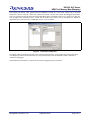
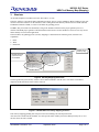
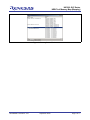
To our customers,
Old Company Name in Catalogs and Other Documents
On April 1st, 2010, NEC Electronics Corporation merged with Renesas Technology
Corporation, and Renesas Electronics Corporation took over all the business of both
companies. Therefore, although the old company name remains in this document, it is a valid
Renesas Electronics document. We appreciate your understanding.
Renesas Electronics website: http://www.renesas.com
April 1st, 2010
Renesas Electronics Corporation
Issued by: Renesas Electronics Corporation (http://www.renesas.com)
Send any inquiries to http://www.renesas.com/inquiry.
Notice
1.
2.
3.
4.
5.
6.
7.
All information included in this document is current as of the date this document is issued. Such information, however, is
subject to change without any prior notice. Before purchasing or using any Renesas Electronics products listed herein, please
confirm the latest product information with a Renesas Electronics sales office. Also, please pay regular and careful attention to
additional and different information to be disclosed by Renesas Electronics such as that disclosed through our website.
Renesas Electronics does not assume any liability for infringement of patents, copyrights, or other intellectual property rights
of third parties by or arising from the use of Renesas Electronics products or technical information described in this document.
No license, express, implied or otherwise, is granted hereby under any patents, copyrights or other intellectual property rights
of Renesas Electronics or others.
You should not alter, modify, copy, or otherwise misappropriate any Renesas Electronics product, whether in whole or in part.
Descriptions of circuits, software and other related information in this document are provided only to illustrate the operation of
semiconductor products and application examples. You are fully responsible for the incorporation of these circuits, software,
and information in the design of your equipment. Renesas Electronics assumes no responsibility for any losses incurred by
you or third parties arising from the use of these circuits, software, or information.
When exporting the products or technology described in this document, you should comply with the applicable export control
laws and regulations and follow the procedures required by such laws and regulations. You should not use Renesas
Electronics products or the technology described in this document for any purpose relating to military applications or use by
the military, including but not limited to the development of weapons of mass destruction. Renesas Electronics products and
technology may not be used for or incorporated into any products or systems whose manufacture, use, or sale is prohibited
under any applicable domestic or foreign laws or regulations.
Renesas Electronics has used reasonable care in preparing the information included in this document, but Renesas Electronics
does not warrant that such information is error free. Renesas Electronics assumes no liability whatsoever for any damages
incurred by you resulting from errors in or omissions from the information included herein.
Renesas Electronics products are classified according to the following three quality grades: “Standard”, “High Quality”, and
“Specific”. The recommended applications for each Renesas Electronics product depends on the product’s quality grade, as
indicated below. You must check the quality grade of each Renesas Electronics product before using it in a particular
application. You may not use any Renesas Electronics product for any application categorized as “Specific” without the prior
written consent of Renesas Electronics. Further, you may not use any Renesas Electronics product for any application for
which it is not intended without the prior written consent of Renesas Electronics. Renesas Electronics shall not be in any way
liable for any damages or losses incurred by you or third parties arising from the use of any Renesas Electronics product for an
application categorized as “Specific” or for which the product is not intended where you have failed to obtain the prior written
consent of Renesas Electronics. The quality grade of each Renesas Electronics product is “Standard” unless otherwise
expressly specified in a Renesas Electronics data sheets or data books, etc.
“Standard”:
8.
9.
10.
11.
12.
Computers; office equipment; communications equipment; test and measurement equipment; audio and visual
equipment; home electronic appliances; machine tools; personal electronic equipment; and industrial robots.
“High Quality”: Transportation equipment (automobiles, trains, ships, etc.); traffic control systems; anti-disaster systems; anticrime systems; safety equipment; and medical equipment not specifically designed for life support.
“Specific”:
Aircraft; aerospace equipment; submersible repeaters; nuclear reactor control systems; medical equipment or
systems for life support (e.g. artificial life support devices or systems), surgical implantations, or healthcare
intervention (e.g. excision, etc.), and any other applications or purposes that pose a direct threat to human life.
You should use the Renesas Electronics products described in this document within the range specified by Renesas Electronics,
especially with respect to the maximum rating, operating supply voltage range, movement power voltage range, heat radiation
characteristics, installation and other product characteristics. Renesas Electronics shall have no liability for malfunctions or
damages arising out of the use of Renesas Electronics products beyond such specified ranges.
Although Renesas Electronics endeavors to improve the quality and reliability of its products, semiconductor products have
specific characteristics such as the occurrence of failure at a certain rate and malfunctions under certain use conditions. Further,
Renesas Electronics products are not subject to radiation resistance design. Please be sure to implement safety measures to
guard them against the possibility of physical injury, and injury or damage caused by fire in the event of the failure of a
Renesas Electronics product, such as safety design for hardware and software including but not limited to redundancy, fire
control and malfunction prevention, appropriate treatment for aging degradation or any other appropriate measures. Because
the evaluation of microcomputer software alone is very difficult, please evaluate the safety of the final products or system
manufactured by you.
Please contact a Renesas Electronics sales office for details as to environmental matters such as the environmental
compatibility of each Renesas Electronics product. Please use Renesas Electronics products in compliance with all applicable
laws and regulations that regulate the inclusion or use of controlled substances, including without limitation, the EU RoHS
Directive. Renesas Electronics assumes no liability for damages or losses occurring as a result of your noncompliance with
applicable laws and regulations.
This document may not be reproduced or duplicated, in any form, in whole or in part, without prior written consent of Renesas
Electronics.
Please contact a Renesas Electronics sales office if you have any questions regarding the information contained in this
document or Renesas Electronics products, or if you have any other inquiries.
(Note 1) “Renesas Electronics” as used in this document means Renesas Electronics Corporation and also includes its majorityowned subsidiaries.
(Note 2) “Renesas Electronics product(s)” means any product developed or manufactured by or for Renesas Electronics.
APPLICATION NOTE
H8/300L SLP Series
HEW Tool Memory Map (Mapping)
Introduction
This document explains the need and usage of memory mapping in development tools.
This involved the usage of the compiler, linkage editor, simulator and emulator.
With an understanding of the concept of memory mapping, users will be able to use the tools more effectively.
Target Device
All H8/300L SLP Series MCU
Contents
1.
Overview ........................................................................................................................................... 2
2.
Compiler and Linkage Editor............................................................................................................. 3
3.
Simulator ........................................................................................................................................... 5
4.
Emulator ............................................................................................................................................ 7
5.
New Device’s Memory Mapping ....................................................................................................... 9
RES06B0001-0100/Rev.1.00
September 2004
Page 1 of 11
H8/300L SLP Series
HEW Tool Memory Map (Mapping)
1.
Overview
Memory mapping is a common term used in the development environment. It is used to prevent programmers from
making mistake, such as:
1. Executing code out of the permitted range in the MCU memory specification
2. Accessing of in-correct memory space
3. Code written to read only memory
Generally user view the memory map of an MCU (Micro-Controller Unit) as:
1.
2.
3.
4.
Internal memory (inside the MCU)
External memory (outside the MCU)
Internal IO area
Reserved area
whereby the internal & external memory may contain:
1. Read only memory (ROM, FLASH, E2PROM, etc.)
2. Read Write memory (RAM)
In a development environment, the tools used will guard against any incorrect access to the area.
In general, the tools will disallow
1. Write to read-only area
2. Access to reserved area
RES06B0001-0100/Rev.1.00
September 2004
Page 2 of 11
H8/300L SLP Series
HEW Tool Memory Map (Mapping)
2.
Compiler and Linkage Editor
The HEW project generator will produce the basic framework based on user’s selection. The selection of CPU, mode,
stack, etc. will determine the setup of the initial section (or memory map).
Example:
Figure 1 Section of a Project
The linkage editor will try to fix the compiled code into the declared sections. If a fix is not possible, a linkage editor
error will be alerted. However a possible fix will only indicate the correctness of the code’s syntax, in which the
generated object code is able to be loaded into the specified MCU memory.
User may change this generated sections to suit to their application need.
Example:
Addition of specified address to force the code to be located at external area.
Figure 2 Addition to Section
RES06B0001-0100/Rev.1.00
September 2004
Page 3 of 11
H8/300L SLP Series
HEW Tool Memory Map (Mapping)
The compiler and linkage editor generated the ELF/DWARF II format file (*.abs) (other formats can be selected).
Unlike the s-record (*.mot) file, which only contains the machine code, this file contains the debugging information.
Users may generate the map file [selection made under HEW Option/ Toolchain/ Link/ List] to view the area where the
code is loaded. This information can be viewed with the MAP Viewer (Please refer to the HEW User Manual or
Application Note “Effective Usage of HEW Map Viewer” for more details)
Figure 3
Generation of Map File
The linkage editor has performed the static level of memory mapping check, for preventing the generated code from
exceeding the specified section declaration. Next, the generated code will be downloaded to either a simulator or
emulator for debugging.
In both simulator and emulator, a dynamic level of memory mapping check is performed.
RES06B0001-0100/Rev.1.00
September 2004
Page 4 of 11
H8/300L SLP Series
HEW Tool Memory Map (Mapping)
3.
Simulator
As the named implied, a simulator will work “like a MCU” on a PC.
Thus user will have to provide the MCU information to the PC prior to a proper simulation. Before loading of user code,
user has to allocated resources for the simulator, such as telling the PC that memory allocation H’0 to H’FFF is ROM,
H’FE00H to H’FFFF is RAM, etc. This is to facilitate the guarding process.
In HEW2, this process has been automated, as long as the simulator checkbox in the project generator process is
checked. The HEW project generator will allocated the initial resources for the simulator to work on. User may need to
further modify it to suit to their application.
In the simulator, the guarding process (memory mapping) is classified into the following terms, which are selfexplainable:
1. Read
2. Write
3. Read-write
Default device
memory map
Default allocated
system resource
for simulator
Figure 4 Memory Mapping Resources
The auto generated system memory resource can be further modified to suit the user’s need. If the reset button is
depressed, all the allocated resource will be removed.
Figure 5 Modification to memory mapping resource
This memory mapping guarding tool will prevent user from loading code into unspecified area.
After the code is loaded into the simulator, user can open the status window [View/CPU/Status] memory tab, to view
the area where the code is loaded
RES06B0001-0100/Rev.1.00
September 2004
Page 5 of 11
H8/300L SLP Series
HEW Tool Memory Map (Mapping)
Figure 6 Memory Status Window
RES06B0001-0100/Rev.1.00
September 2004
Page 6 of 11
H8/300L SLP Series
HEW Tool Memory Map (Mapping)
4.
Emulator
Unlike the simulator, the emulator uses the actual or bond-out chip to execute the user codes. Thus the memory
mapping control will be more sophisticated than the simulator.
In the emulator context, there are three memory areas:
1. On-chip memory
2. External memory
3. Emulator memory
Among these memories, there are three kind of classification:
1. Read-only
2. Read/write
3. Guarded
Thus user can have nine memory mapping selection based on the above combination:
1. On-chip read-only
2. On-chip read/write
3. On-chip guarded
4. External read-only
5. External read/write
6.External guarded
7. Emulator read-only
8. Emulator read/write
9. Emulator guarded
Technically, on-chip guarded, external-guarded and emulator-guarded are equivalent.
RES06B0001-0100/Rev.1.00
September 2004
Page 7 of 11
H8/300L SLP Series
HEW Tool Memory Map (Mapping)
4.1
On-Chip Memory
This memory refers to the available internal memory in the MCU (RAM, ROM, and IO).
When access is concerned, this will be 1st priority in the emulator.
• If user has physically connected an external memory to address H’0 – H’1FFF which is also the on-chip ROM area,
the external memory will be ignored (no conflict will happen).
4.2
Emulator Memory
As compared to the actual chip and simulator, emulator memory is considered a new term used. This memory is
provided as a temporary mean when the target memory is not available (e.g. target hardware fabrication is not ready)
Thus it is a substitute for External memory.
When access is concerned, this will be 2nd priority in the emulator.
• If a target memory is available and it is mapped to area 2. When the emulator memory is also set to area 2, this
emulator memory will be accessed instead of the external memory (no conflict will occur)
4.3
External Memory
This memory refers to the memory mapped to the external area of the MCU
When access is concerned, this will be last priority in the emulator.
4.4
Read-Only
When any type of memory is classified as read-only, any attempt to write to this area, will cause a break to the normal
execution. This break is named as “write protected break”
4.5
Guarded
An area is guarded if it is a reserved or protected area. Thus any attempt to access (read or write) this area, will generate
a break. This break is named as “Guarded break”
4.6
Read/Write
Any other area that are not read-only or guarded is considered as read/write area. It allows program to read or write to
the area.
RES06B0001-0100/Rev.1.00
September 2004
Page 8 of 11
H8/300L SLP Series
HEW Tool Memory Map (Mapping)
5.
New Device’s Memory Mapping
The followings give programmer a quick start guide in generating their memory mapping control when the device
mapping data is not available yet.
In general, when a new device is introduced, it can fall into few categories
• New core, a new family, a new series
Code Writing:
The advice is to select the nearest family/series for the project creation, and modify the section & <iodefine.h> file,
based on the new device specifications (ROM, RAM, and IO address).
Let take an example based on the H8S/2215 (assuming it is a new device). From the H8S family device introduction
and roadmap, programmer can know that the H8S/2238 is an ancestor of the H8S/2215. The differences between the
two devices are:
• ROM, RAM sizes, and
• Addition of USB peripherals
To begin writing code for the H8S/2215, programmer can
• Generate the code based on the H8S/2238.
• Modify the section file for ROM/RAM boundary
• Add the structure definition for all the USB registers, and define the address.
Simulator:
Since simulator cannot simulate the IO, Programmer can select a close family to simulate the device. The only possible
changes are the ROM & RAM boundary address.
Emulator:
However, complications will arrive in the case of emulator. User has to find out the ability of the emulator to support
the new device.
• If its does (when device information is not available), then the user can only use the tool, to emulate the new device
to a substantial level.
Example: when selecting the H8S/2238 to emulate the H8S/2215, user will not be able to emulate the USB
peripherals. Other peripherals are performing as it is (IO addresses are identical)
• However if the new device is a mere ROM and RAM size different, user will be able to perform emulation, as long
as their program do not exceed the memory size boundary.
Example: The H8S/2144 is a smaller version of the H8S/2148
In summary, user can perform immediate emulation as long as the generated code is running on the correct core.
However it is still advisable to obtain the latest device information from the support groups.
RES06B0001-0100/Rev.1.00
September 2004
Page 9 of 11
H8/300L SLP Series
HEW Tool Memory Map (Mapping)
Revision Record
Rev.
1.00
Date
Sep.10.04
RES06B0001-0100/Rev.1.00
Description
Page
Summary
—
First edition issued
September 2004
Page 10 of 11
H8/300L SLP Series
HEW Tool Memory Map (Mapping)
Keep safety first in your circuit designs!
1. Renesas Technology Corp. puts the maximum effort into making semiconductor products better and
more reliable, but there is always the possibility that trouble may occur with them. Trouble with
semiconductors may lead to personal injury, fire or property damage.
Remember to give due consideration to safety when making your circuit designs, with appropriate
measures such as (i) placement of substitutive, auxiliary circuits, (ii) use of nonflammable material or
(iii) prevention against any malfunction or mishap.
Notes regarding these materials
1. These materials are intended as a reference to assist our customers in the selection of the Renesas
Technology Corp. product best suited to the customer's application; they do not convey any license
under any intellectual property rights, or any other rights, belonging to Renesas Technology Corp. or
a third party.
2. Renesas Technology Corp. assumes no responsibility for any damage, or infringement of any thirdparty's rights, originating in the use of any product data, diagrams, charts, programs, algorithms, or
circuit application examples contained in these materials.
3. All information contained in these materials, including product data, diagrams, charts, programs and
algorithms represents information on products at the time of publication of these materials, and are
subject to change by Renesas Technology Corp. without notice due to product improvements or
other reasons. It is therefore recommended that customers contact Renesas Technology Corp. or
an authorized Renesas Technology Corp. product distributor for the latest product information
before purchasing a product listed herein.
The information described here may contain technical inaccuracies or typographical errors.
Renesas Technology Corp. assumes no responsibility for any damage, liability, or other loss rising
from these inaccuracies or errors.
Please also pay attention to information published by Renesas Technology Corp. by various means,
including the Renesas Technology Corp. Semiconductor home page (http://www.renesas.com).
4. When using any or all of the information contained in these materials, including product data,
diagrams, charts, programs, and algorithms, please be sure to evaluate all information as a total
system before making a final decision on the applicability of the information and products. Renesas
Technology Corp. assumes no responsibility for any damage, liability or other loss resulting from the
information contained herein.
5. Renesas Technology Corp. semiconductors are not designed or manufactured for use in a device or
system that is used under circumstances in which human life is potentially at stake. Please contact
Renesas Technology Corp. or an authorized Renesas Technology Corp. product distributor when
considering the use of a product contained herein for any specific purposes, such as apparatus or
systems for transportation, vehicular, medical, aerospace, nuclear, or undersea repeater use.
6. The prior written approval of Renesas Technology Corp. is necessary to reprint or reproduce in
whole or in part these materials.
7. If these products or technologies are subject to the Japanese export control restrictions, they must
be exported under a license from the Japanese government and cannot be imported into a country
other than the approved destination.
Any diversion or reexport contrary to the export control laws and regulations of Japan and/or the
country of destination is prohibited.
8. Please contact Renesas Technology Corp. for further details on these materials or the products
contained therein.
RES06B0001-0100/Rev.1.00
September 2004
Page 11 of 11