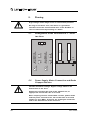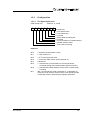
1
EcoServ ND 31
User Manual
Servoconverter ND 31
Subject to change without notice
Lenord, Bauer & Co. GmbH
Dohlenstraße 32
D-46145 Oberhausen
Tel. +49/208/9963-0
Fax +49/208/676292
E-Mail: [email protected]
Internet: http://www.lenord.de
09/98
INDEX
1. General ........................................................................................................... 5
1.1 About this Documentation ......................................................................................5
1.2 Customer Service...................................................................................................6
1.3 Designation.............................................................................................................6
1.4 Rights .....................................................................................................................6
2. General Safety Remarks................................................................................ 7
2.1 Proper Usage .........................................................................................................7
2.2 Organizational Measures........................................................................................8
2.3 Safety Units ............................................................................................................8
2.4 High Voltage ...........................................................................................................8
2.5 Contact Protection Compact Device ......................................................................9
2.6 19” Drawer Devices ..............................................................................................10
3. Functional Description ................................................................................ 12
3.1 General.................................................................................................................12
3.2 Power Supply........................................................................................................12
3.3 Automatic Control Part .........................................................................................13
4. Technical Data.............................................................................................. 14
4.1 Nomenclatures .....................................................................................................14
4.2 Electrical Data ......................................................................................................15
4.2.1 Power Supply Connection..........................................................................15
4.2.2 Intermediate Circuit and End Amplifier ......................................................16
4.2.3 Ballast Switching........................................................................................17
4.2.4 Ventilation Compact Device.......................................................................18
4.2.5 Usable Connectors ....................................................................................18
4.2.6 Resolver.....................................................................................................19
4.3 Mechanical Data...................................................................................................19
4.3.1 Measurements ...........................................................................................19
4.3.2 Weight .......................................................................................................19
4.3.3 Environment Conditions.............................................................................19
5. Pinning.......................................................................................................... 20
5.1 Arrangement of the Connectors X1…X5 for two Axes.........................................20
5.2 Power Supply, Motor Connection and Brake Chopper Resistor...........................20
5.3 Resolver Connection (X2) ....................................................................................23
5.3.1 Feedback System Resolver (X2)...............................................................24
5.4 Peripheral Equipment Connection (X3)................................................................24
5.4.1 Analogue Input...........................................................................................26
5.4.2 Analogue Output........................................................................................26
5.4.3 Digital Input: Group 1.................................................................................27
5.4.4 Pulse Inputs ...............................................................................................27
5.4.5 Digital Outputs ...........................................................................................28
5.4.6 Encoder Emulation ....................................................................................29
5.4.7 Ready for Operation Contact .....................................................................29
5.5 Bus Coupling ........................................................................................................30
ND31-UM0998
1
5.5.1 Serial Interface - Output Plug X4 .............................................................. 30
5.5.2 Serial Interface - Input Plug X5 ................................................................. 31
5.6 Fan Connection ................................................................................................... 32
5.7 Connection Example ........................................................................................... 33
6. Installation ................................................................................................... 34
6.1 Mechanical Installation ........................................................................................ 34
6.2 Fuselage .............................................................................................................. 34
6.3 Earthing and Shielding......................................................................................... 35
6.4 Emergency Power Off Concept ND31................................................................. 37
6.4.1 General ..................................................................................................... 37
6.4.2 Short Circuit Braking ................................................................................. 38
6.4.3 Emergency Power Off with Controlled Braking........................................ 39
7. Designing a Drive Unit ................................................................................ 41
7.1 Electrical Design .................................................................................................. 41
8. Novobus ....................................................................................................... 43
8.1 General ................................................................................................................ 43
8.2 Features .............................................................................................................. 44
8.3 Requirements for Transmission .......................................................................... 44
8.4 Bus Structure....................................................................................................... 45
8.5 Device Addresses................................................................................................ 45
9. Bus-Definition.............................................................................................. 46
9.1 Transmission Syntax ........................................................................................... 46
9.2 Synchronization Byte ........................................................................................... 46
9.3 Address Byte ....................................................................................................... 47
9.4 Process Data Bus................................................................................................ 48
9.5 Parameter Bus..................................................................................................... 48
9.6 Control Byte in the Parameter Bus ...................................................................... 48
9.7 Error Handling...................................................................................................... 49
9.8 Checking Sequence ............................................................................................ 51
9.9 Time-out Error ..................................................................................................... 53
10. CAN Bus ..................................................................................................... 54
10.1 Data exchange with Controllers GEL 8100 ....................................................... 54
10.2 CAN bus configuration....................................................................................... 54
11. ND31 Specific Commands ........................................................................ 55
11.1 Read Commands............................................................................................... 55
11.2 Write Commands............................................................................................... 56
11.3 Bit Manipulation and Logical Commands .......................................................... 57
11.4 Input/Output Commands ................................................................................... 57
11.5 Reset H8............................................................................................................ 57
12. Set-up and Output Capabilities of the EcoServ....................................... 58
12.1 Requirements .................................................................................................... 58
2
ND31-UM0998
12.2 EcoServ Memory ................................................................................................58
12.2.1 RAM Memory...........................................................................................59
12.3 Configuration ......................................................................................................65
12.3.1 The Byte SwVersion ................................................................................65
12.3.2 The Byte HwVersion ................................................................................66
12.3.3 The Byte Feedback..................................................................................66
12.3.4 The Byte Betriebsart ................................................................................67
12.3.5 The Byte MotConfig .................................................................................68
12.4 ND31 Status .......................................................................................................69
12.4.1 The Byte Status .......................................................................................69
12.4.2 The Byte Freigabe0 .................................................................................69
12.4.3 The Byte NBcontrol..................................................................................70
12.4.4 The Byte CANcontrol ...............................................................................70
12.4.5 The Byte NB_Init......................................................................................71
12.5 Actual, Nominal and Limit Values.......................................................................71
12.5.1 Current.....................................................................................................71
12.5.2 Torque .....................................................................................................72
12.5.3 Speed ......................................................................................................72
12.5.4 Ramps .....................................................................................................73
12.5.5 Tracks ......................................................................................................73
12.6 Temperatures .....................................................................................................74
12.6.1 Cooler Temperature ................................................................................74
12.6.2 Motor Temperature..................................................................................74
12.7 Regulator Parameter ..........................................................................................74
12.7.1 Current Regulator ....................................................................................75
12.7.2 EMF Compensation .................................................................................75
12.7.3 Filter.........................................................................................................75
12.7.4 Speed Regulator......................................................................................76
12.7.5 Position Regulator ...................................................................................76
12.7.6 Resolver Adjustment................................................................................76
12.8 Signal Inputs and Outputs ..................................................................................77
12.8.1 Digital Signals ..........................................................................................77
12.8.2 Analogue Outputs ....................................................................................79
12.8.3 Encoder Emulation ..................................................................................80
12.9 Drive Info ............................................................................................................80
12.9.1 Serial Number..........................................................................................80
12.9.2 Operating Hours ......................................................................................80
12.10 Controlling the ND31 via NOVOBUS................................................................80
12.10.1 Operating States....................................................................................81
12.10.2 Error Condition.......................................................................................81
12.11 Oscilloscope .....................................................................................................81
12.11.1 Signal Selection .....................................................................................81
12.11.2 Time Base..............................................................................................82
12.11.3 Triggering Threshold..............................................................................82
12.11.4 Trigger Delay .........................................................................................82
12.11.5 Scope Status .........................................................................................83
12.11.6 Recording Procedure.............................................................................83
12.11.7 Auto Trigger ...........................................................................................84
12.12 Resolver Auto Adjustment................................................................................84
12.13 Brake Function .................................................................................................84
ND31-UM0998
3
This page intentionally left blank
4
ND31-UM0998
1.
General
1.1
About this Documentation
The documentation for your EcoServ ND31 consists of 3
components:
• (This) User Manual
This section is for users who are project managers, deers and
software developers. Here you will find the information needed
for designing a system using the EcoServ.
• Set-up and Parameter Setting
This section is for developers and technicians who must perform
the set-up and configuration of the ND31. It will be sent on
request with ND31 delivery.
• Instructions for Installation and Replacement
These instructions are for technicians and electricians who must
install or replace the ND31. This flyer will be enclosed with ND31
delivery.
The symbols below will be used in this manual. These symbols
will assist you in quickly finding important information.
The commonly used danger symbol, identifies text passages
that must, by all means, be read and clearly understood! Not
observing these passages could endanger the life and health
of yourself and others.
ATTENTION!
ND31-UM0998
Text passages marked with “ATTENTION” must, by all
means, be read and clearly understood! Ignoring these
passages could lead to the destruction or damaging of the
EcoServ or the machine in which it is installed.
5
1.2
Customer Service
Lenord, Bauer & Co. GmbH
Dohlenstraße 32
D - 46145 Oberhausen
Telefon: +49-208-9963-0
Fax +49-208-9963-201
1.3
Designation
N D 31 32 XX X S X X X 0 0 0
0 - no table interpolation
0 - 8k mem ory
0 - R esolver
0 - NO VO BUS
1 - CA N -B us
0 - reserved
0 - reserved
S - sinus s haped c omm utation
V
X
02
04
07
12
32
-
19" m odule
comp act device
2 A power m odule
4 A power m odule
7 A power module
1 2 A power module
320 V intermediate circuit voltage
31
- devic e series
ND
1.4
Rights
IBM is a registered trademark of the IBM Corporation.
6
ND31-UM0998
2.
General Safety Remarks
There are operating voltages in the ND31 that can be fatal!
Wiring
Saftey
Components
Therefore, check the wiring of the ND31 before switching it on.
Ensure that all plugs are properly inserted and grounding has
been properly performed.
Ensure that no voltage carrying parts can be accidentally touched
and all safety components of the ND31 are present and properly
connected.
Emergency
Power-Off
Provide an “Emergency Power Off” switch so the motor can be
switched off at anytime.
Electrolytic
Capacitor
After power-off the electrolytic capacitor takes approximately one
minute to unload! This means: One minute after power-off, fatal
voltages are still present in the device. During this time period
nothing is to be touched.
Voltage
In case the motor continues to turn after the power supply has
been switched off, the fatal voltage can be prolonged until a total
stop occurs. Only then the unloading of the electrolytic capacitor
begins.
On and Off
Switching
Order of
Switching On
Avoid excessive, repeated and rapid on and off switching of the
power supply, this could overload the switching current limiter of
the ND31. This overloading can lead to the destruction of the limit
switch limit resistance.
W hen switching on, the power supply connection should be set
first for the automatic control part before switching on the power
supply. W hen switching off please proceed reverse.
2.1
EcoServ ND31
Proper Usage
The frequency converter EcoServ ND31 is a pulse and frequency
converter for controlling brushless servo and asynchronous
motors. It is a state of the art converter. Using the converter for
an application other than described here, can be damaging to the
health of the user or others. Also, the converter the drive or other
valuable items can be damaged.
Only use the converter when error free conditions are provided.
Always regard safety rules and regulations. Be aware of the
manuals and abide the warnings provided.
ND31-UM0998
7
Compatible
Motors
Regulations
Operating
Environment
Use only brushless servo motors and asynchronous motors with
technical data compatible to the converter and its specifications.
Install the converter only in conformance to the local
specifications, standards and regulations.
Do not operate the converter in areas with danger of explosions
or in range of medical devices.
Exceptions: The converter is encased in a housing designed,
tested and specified for operation in these applications.
2.2
Saftey Measures
Qualified Stuff
Organizational Measures
As manufacturer and distributor of a machine in which this
converter is used, you are responsible for ensuring that all
accident prevention and safety measures have been taken.
Ensure that installation and maintenance is only performed by a
qualified electrician.
Ensure that the set-up is only performed by trained personnel.
During installation, the safety warnings in this manual are to be
observed.
Manuals
Transport and
Storage
The designer or developer of a machine in which the converter is
installed has read and understood the warnings in the manuals.
For the transport and storage of the converter the original
packing has to be used.
2.3
Emergency
Power-Off
Safety Units
Machines with moveable parts which are hazardous to people or
the machine, must be equipped with an emergency power-off
(EPO). Install the EPO as described in Chapter 6, Installation.
2.4
High Voltage
The converter works with hazardous high voltage. Read and
abide to the following points.
Ensure that no parts carrying voltage can be accidentally
touched.
• Install fuses as described in Section 6.2, Fuselage.
• Emergency Power-off-Installation as described in Section 6.4,
Emergency Power Off Concept ND31.
8
ND31-UM0998
• Ensure that proper grounding is provided.
• Make all connections in accordance with Chapter 5, Pinning.
• Do not disassemble the device. Do not make any changes to
the device. Repairs may only be made by the manufacturer.
During set-up, abide to all safety regulations and ensure that
safety features are provided.
2.5
Contact Protection Compact Device
Requirements: Protect against dangerous body current (Draft
DIN VDE 160 11.94 Section 5.2.).
The following measurements are necessary to fulfill the
requirements above.
• Pulling or inserting the plug of the ND31 is to be nonpermissive, when the device is under voltage. Power is only to
be applied to the ND31 when all connections screwed to the
ND31 are protected against accidental slipping. W orking on
the plugs of the ND31 is not to be performed when the device
is under voltage. All connection are only to be made by a
qualified electrician.
• Opening the housing is not allowed!
• Before the power supply is switched on for the first time,
ensure all cables have been checked to confirm proper
isolation of all wires.
• This is to be repeated at each maintenance interval. Loose
clamps are to be retightened. Ensure cables to moveable
components, connected to the ND31, are relieved of tension.
Protected by isolating active components (Draft DIN VDE
0160 11.94 Section 5.2.3.).
• A minimum of basic isolation protects the active components
from the metal housing. The housings must be grounded! A
grounding screw for this purpose is provided on the metal
housing.
2
A wire with a diameter >= 10 mm CU is required for
grounding.
Periphery Plug X3
Safe isolation of all signals of the periphery plug X3 from active
components is already provided in the ND31 by double isolation
(Draft DIN VDE 160 11.94 Section 5.2.18.2.).
ND31-UM0998
9
Resolver Plug X2
The safe isolation of all signals from the active components of
the ND31 is required by double isolation.
Power Connection X1
The connection cable and wiring must have a doubled or
reinforced isolating between the wires and the surface (Draft DIN
VDE 160 11.94 5.3.1.1.).
The connection area is to be protected against accidental
contact. Before the power supply is switched on, all cables are to
be checked and tested for proper isolation.
Clamps for the respective wire sizes are to be used on the ends
of wires.
Bus Connections X4 and X5
The signals of the bus are already separated from active
components of the ND31 by double isolation. The housing of the
connection cable must have a non-conducting surface.
2.6
19” Drawer Devices
Requirements: Protection against dangerous body current
(Draft DIN VDE 160 Section 5.2.1.).
• Pulling or inserting the plug connections of the ND31 is nonpermissive when the device is under current. Power is only to
be connected to the ND31 when all plugs are protected
against slipping by screwing them to the 19” frame or the
ND31. W orking on the plugs of the ND31 or the 19” frame is
not permitted as long as the ND31 is under current. W orking
on the connections is only to be performed by a qualified
electrician.
• The removal of the ND31 from the 19” frame is only to be
performed in a power down situation and from a trained
electrician. Before the ND31 is first turned on, a check is to be
made for proper seating, and all cables are to be checked for
proper isolation. This is to be repeated at each maintenance
interval of the machine. Loosened screws are to be retightened.
• The connection area on the back panel of the 19” frame must
be protected against accidental contact. Cables leading to
movable components in the machine must be protected
against being pulled out of the 19” frame.
10
ND31-UM0998
Requirements: Protection by isolating active components
(Draft DIN VDE 160 Section 5.2.3.).
• A minimum of basis isolation of the active components against
the metal housing is provided. The 19” housing must be
grounded. Grounding is performed by using the screw
provided on the housing of the 19” drawer.
• A wire with a diameter >= 10 mm CU is required for
grounding.
2
• The 19” frame, the side post of the frame, the cover plate, the
ventilator draw and the front panel are separated from the
active components of the ND31 by double isolation.
Periphery plug X3
(See Section 2.5, Contact Protection Compact Device)
Resolver plug X2
(See Section 2.5)
Power plug X1
(See Section 2.5)
Bus Connection X4 and X5
(See Section 2.5)
ND31-UM0998
11
Servo Converter
3.
Functional Description
3.1
General
The ND31 is a servo converter for permanently active
synchronized servo motors.
Inputs and
Outputs
The ND31 is equipped with all the usual control and signal inputs
and outputs such as, enable regulator, ready signal, limit switch
etc.
Setting Up
Setting up the ND31 is performed with a laptop PC. The memory
oscilloscope function built into the ND31 offers the possibility, to
display all nominal and actual value courses of the current,
torque, speed and rotor position on the laptop monitor without
excessive measuring techniques.
This makes adjusting the ND31 very easy, since the effects of
parameter change can immediately be evaluated. Parameters are
stored in the ND31 and saved on a disc. Parameter lines can be
repeatedly copied to other ND31s.
NOVOBUS
CAN-Bus
Drives can be connected with a controller via NOVOBUS. A ringshaped wiring is required. Hardware components are not
required. The transmission medium is the standarized, serial
interface RS232 or RS485.
Additionally Novotron offers the CAN-Bus for ND31. CAN-Bus
means a cheap solution for networking controller and ND31 and
ND31 among each other.
3.2
Circuit Connector
DC Circuit
Power Supply
ND31 is equipped with all components required for a positioning
axis. This includes a power supply for directly connecting the
ND31 to the 230V AC circuit. Protective switches limit the jolt of
switching-on current and protect the ND31 from circuit over
voltage and transients.
The braking energy of the motor is absorbed in an intermediate
DC circuit. If the capacity of the intermediate circuit condensor is
insufficient, the built-in brake chopper becomes active to prevent
a too high of an increase in the intermediate circuit voltage.
W hen inserting several ND31 it is additionally possible to couple
the intermediate circuits. Therefore the energy of the brake can
be devided in several intermediate capacitors. The intermediate
circuit of ND31 must not be connected parallel to the
intermediate circuit of other manufacturers.
12
ND31-UM0998
W hen inserting several intermediate circuits of several ND31 you
have to abide the same pinning of the different power connection
P1, P2 and P3. Avoid exchanging the phases, this could lead to
the destruction of the drive.
Ballast Switching
Circuit-Breaker
The internal ballast switching is checked electronically. On
overloading the ballast switching stops and ND31 changes to
overload.
A IGBT converter provides the motor with current. All motor
cables are short circuit proof. All power circuits are isolated from
the regulator.
3.3
Automatic Control Part
For the internal power supply of the drive a 24 VDC-power supply
is necessary.
Position
The position, speed and voltage regulation as well as the pulse
width modulation in the ND31 is performed digitally. The voltage
regulation and the pulse width modulation are integrated in the
ND31 ASIC („Potential Chip“ ND32XX), developed especially for
the ND31. Another ASIC („Periphery Chip“ ND31XX) integrates a
resolver converter, ROD-impulse counter, coordinates
transformer and the encoder emulator.
Feedback
The remainder of the technical regulator functions are performed
by a Hitachi H8/330 micro controller. ND31 needs a resolver for
its feedback system in the motor or an optical signal provider.
The ND31 can also be used for analyzing multi turn resolvers.
The resolver or digital conversion is performed by the periphery
chip ND31XX. The resolution of the rotor position measuring is
16 bits.
Nominal Values
The following choice of possibilities are available for the nominal
value input:
• Analogue +/- 10V
• Incremental encoders
• Frequency and direction impulse
• Digital nominal value input via the no cost sensor actor bus
NOVOBUS (RS232/485)
• CAN-Interface
ND31-UM0998
13
Ratings
Signal Processing
14
4.
Technical Data
4.1
Nomenclatures
Over Voltage Stability
IEC 801-4 Class 2
Radio Interference
EN55011 Class A is upheld by using the
line filter
Isolation Concept
Double isolation between power supply
and controller
Check
Referring VDE160 11.94 Chapter 9.1.1.
Protection Type
ND31 32XX VS IP00
(Protection Type is determined by
19“frame)
ND31 32XX XS IP20 to DIN 40050 and
IEC144
Serial interface
RS232: ANSI/EIA232D
RS485: EIA485
Modulation of the output
transformer
Digital pulse width modulator
Modulation procedure
Modified sinus-triangle procedure
Current regulator
Digital PI-regulator with EMK-compensation, symmetrical limiter and anti-wind-up
switch
Resolution of motor
current measurement
11 bit
Speed regulator
Digital PI-regulator with velocity advanced
control and anti-wind-up switch
Position controller
Digital P-controller with velocity advanced
control
Position relay system
Resolver or optical impulse supply
Absolute path measuring
system
Absolute resolver supports the system
IMAS from the company Baumer Electric
(if required). Optical multi-turn-position
sensor with SSI-interface
ND31-UM0998
Motor temperature probe
Communication
Selection: Opener or PTC
Communication protocol
RS232/485, communication protocol:
NOVOBUS
CAN-Interface
Specification CAN2.0 part A and B
ISO/DIS 11898
Frequency/directioninterface
Entrance, RS422. Stepping motor
emulation with a maximum frequency of
500kHz
Encoder entrance
Difference inputs, RS422 standard.
ROD426
Analogue interface
±10V 14bit
±10V 8bit
0...5V 8 bit
4.2
Electrical Data
4.2.1
Power Supply Connection
Device type ND31-
3202
3204
3207
3212
Connecting rated
voltage
230VDC
230VDC
230VDC
230VDC
Input frequency
50/60Hz
Voltage range for
connection
20 ... 240 VAC +10%
2/3
Number of input
phases
Connecting value
for rated current
0,75kVA
1,5kVA
3
2,7kVA
4,5kVA
Periodical and not periodical transient over voltage:
Acceptable
transient energy at
the connection
ND31-UM0998
10 Ws
15
Half life period
1.2/50µs
Periodical peak
value
380V
Unique peak value
2000V
(on 2
Ohm)
160A
160A
160A
160A
Security (3phases)
3x4A
inert
3x8A
inert
3 x 14 A
inert
3 x 24 A
inert
(1phase)
6A inert
12A inert
15A inert
not possible
Max. switching
current (internally
limited)
Power supply
24VDC ± 15% external, 1A
Power consumption 24 W plus approx. 2.5 W per each controlled
output
4.2.2
Intermediate Circuit and End Amplifier
Device type ND31-
3202
3207
DC rail voltage with voltage
connection
320 V
Shut-off threshold with overvoltage
430 V
3212
programmable (<30V)
Shut-off threshold with undervoltage
3
Number of output phases
16
3204
Output voltage
300Veff
Loading class
III
Loading type
Motor
load
Intermediate circuit capacity
480
480
480
1320 µF
Power-loss in the output
transformer at rated current in
Watt
40
50
60
100
ND31-UM0998
4V
Remaining voltage-loss with
rated current
End amplifier tact frequency
9.76
9.76
9.76
9.76 kHz
Motor tact frequency
19.5
19.5
19.5
19.5 kHz
Rated current Tu = 25°C
2
4
7
12 Aeff
Peak current Tk = 25°C
4
8
14
24 Aeff
Maximum output current in relation to the cooler temperature:
Temp
25
35
45
55
65
75
85
°C
3202
4
3,8
3,5
3,1
2,7
2,4
2
Aeff
3204
8
7,6
6,9
6,1
5,4
4,7
4
Aeff
3207
14
13,3
12
10,6
9,5
8,2
7
Aeff
3212
24
22,8
20,6
18,2
16,3
14,1
12
Aeff
As long as the cooler temperature remains at the given value,
these currents on 3202, 3204 and 3207 are valid without time
limitation. On 3212 the peak current is limited after 5 seconds.
Note: W ith good external venting and an environment
temperature of 40°C and 7 A eff motor current, the cooler
reaches a temperature with ND31-3207 of approx. 75°C.
4.2.3
Ballast Switching
Continuous duty loss
Pulse power ballast
switching
ND31-UM0998
Internal ballast
switching
34 W
(with external
venting 68W)
Internal ballast
switching ND31 3204,
3207 and 3212
68 W
(with external
venting 130W)
External ballast
switching for ND31
3203 (2 A device)
max. 500W
External ballast
switching for ND31
3204, 3207 (2 A and
4A device)
max. 2kW
ND31 3202 (2 A
device)
2,5 kW
17
Maximum ballast energy
of the in-built ballast
resistor
5 kW
ND31 3212 (12 A
device)
8 kW
3202
200 Ws
3204 u. 3207
400 Ws
3212
600Ws
Repetition rate of the
maximum ballast energy
with the built-in ballast
resistor
4s
Switching threshold
(Threshold automatic)
420 V
Resistance for external
ballast switching
4.2.4
ND31 3202
50 Ohm
ND31 3204, 3207
25 Ohm
Ventilation Compact Device
Ventilation
External ventilation (built-in)
Connection
Voltage connection: 230 VAC
Current capacity: < 200 mA
Fuselage
315 mA inert
4.2.5
18
ND31 3204, ND31
3207 (4 A and 7 A
devices)
Usable Connectors
Connection for power supply X1
5605,5610,5615, 5620
Phönix Combicon
Front-GMSTB 2,5/16-STF
Resolver connection and motor
temperature probe X2
High Density D-SUB 15pol (on the
ND 21: socket contacts)
Periphery connection X3
SCSI 68 pole (on the ND31: socket
contacts)
Bus output connection X4
D-SUB 9pol (on the ND31: pin
contacts)
Bus input connection X5
D-SUB 9pol (on the ND31: socket
contacts)
ND31-UM0998
4.2.6
Resolver
Resolver:
Sagem: 21RX360407, 15RX310107
Litton: JSSBH-15 E-5, JSSBH-21-P4
Siemens: V23401-H2001-B202
Tamagawa: TS2018N321 E52, TS2112N21 E11
19“Module
4.3
Mechanical Data
4.3.1
Measurements
3202, 3204, 3207
229 mm x 100 mm x 45,4 mm
3212
229 mm x 100 mm x 91 mm
4.3.2
3202, 3204, 3207
0,7 kg
3212
1,4 kg
4.3.3
Storage
Temperature
Operating
Temperature
ND31-UM0998
Weight
Environment Conditions
max. storage temperature
-25°C to +70°C
max. humidity
95 %
Operating temperature
0°C to 70°C
rel. humidity
20 - 75 %
Altitude over NN
Up to 1000 m over NN power decrease
must be expected.
19
5.
Pinning
High voltage! Fatal danger even in switched-off position!
As long as the motor runs, the motor is a generator!
Therefore avoid the uncontrolled drive of the EcoServ in
case of interference by building in a brake.
5.1
Arrangement of the Connectors X1…X5 for
two Axes
Top view
5.2
Power
X1.2
Power
X1.1
X4.2
Bus Out
X5.2
Bus In
PE
(Line)
X2.2
Resolver
X3.2
Peripheral Equipment
X4.1
Bus Out
X5.1
Bus In
X2.1
Resolver
X3.1
Peripheral Equipment
Fan
Bottom view
Power Supply, Motor Connection and Brake
Chopper Resistor
230 VAC maximum voltage. Higher voltage leads to the
destruction of the drive.
Should the converter be used at the 400VAC-net, an
appropriate transformer has to be used.
When coupling various intermediate circuits, please abide
that the power connection P1, P2 and P3 have to be used
equally on each ND31. If phases are exchanged could that
lead to the destruction of the converter.
20
ND31-UM0998
Plug X1
16-pole Combicon
Note: The following pinning may serve as an example. Pinning
for other motors may differ from this (refer to the concerning connection table).
Pinning
Pin
External brake chopper resistor
(option) ***)
1 eB
extBAL
Internal brake chopper resistor ***)
2 iB
intBAL
+ Ballast switching
3B
+BAL
4
-
Open
Transformer
One phase
power supply
Power supply(max. 230 VAC)
5 E1
P1 ****)
open
Power supply (max. 230 VAC)
6 E2
P2 ****)
N
Power supply (max. 230 VAC)
7 E3
P3 ****)
L****)
- Intermediate circuit
8 –Z
-ZKS
+ Intermediate circuit
9 +Z
+ZKS
Motor connection
10 A3
C **)
Motor connection
11 A2
B **)
Motor connection
12 A1
A **)
Ground
13 PE
PE
Ground
14 PE
PE
Motor temperature probe *)
15 T1
TempMot
Motor temperature probe *)
16 T2
TempMot
Notes:
ND31-UM0998
*)
If the motor temperature probe is wired with the motor
cable, please connect here.
**)
SBL/SBK motors refer as follows: A → U, B → V, C → W .
21
***)
If the built-in brake chopper resistor should be used please
insert a wire bridge between pins 2 and 3.
If you would like to use the external brake chopper: do not
insert a wire bridge between pins 2 and 3. Connect the
brake chopper resistor at pins 1 and 3.
****) The ND31 converter can be used with a max. power supply
of 230VAC. If you would like to operate the converter in the
400VAC mains, please use an appropriate transformer.
Cross-Section of
the Power Supply
Cable
Type ND31-
3202
3204
3207
3212
Main supply 4 x
1,5
1,5
2,5
2,5mm²
Motor connection 4 x
(without brake)
1,5
1,5
2,5
2,5mm²
Inner circuit-bus 2 x
1,5
1,5
2,5
2,5mm²
Brake chopper resistor 2 x
1,5
1,5
2,5
2,5mm²
All cables shielded.
Isolation
The used cables and wires must have a double or reinforced
isolation between core and surface (Draft DIN VDE 160 11.94
5.3.1.1.).
Fuselage
Type ND31-
3202
3204
3207
3212
3 phases (230VAC)
3x4A
inert
3x8A
inert
3 x 14A
inert
3 x 24 A
inert
1 phase (230VAC)
6A
inert
12A
inert
not
possible
not
possible
If several drives are to be fused together, for the whole you have
to count the sum of each device.
Motor Connection
The motor has to be connected with a shielded cable on
connector X1 of ND31. The cable shield has to be based on
ND31 and the motor (the shield is based on both sides). On The
assigned cable clamps have to be used on ND31.
The wire cross section can be interpreted according to the
expected motor current. See VDE 0113, German issue of EN
6204:
Electric
Loading
22
Rated cross
section
0.75
mm²
1.00
mm²
1:50
mm²
2.50
mm²
4
mm²
ND31-UM0998
Rated current
7.5
Aeff
10
Aeff
13
Aeff
18
Aeff
25
Aeff
The used cables and wires must have a double isolation between
core and surface (Draft DIN VDE 160 11.94 5.3.1.1).
For the cable ends cable-end-sleeves with isolation in the
corresponding size have to be used.
The connection area has to be fused against accidentally
touches. Before switching on the supply voltage please
ensure that the fitting of all cables have been controlled
and examined as well as the isolation of all cable ends.
The earthing connection has to be made on the therefore
assigned earthing bolt on the housing of the compact device or
on the rear wall of the 19“ rack.
Recommended motor cables: Lütze Silflex NSY, Lapp Ölflex 400CP
Brake Chopper
Resistor
The value of the external ballast switching has to be 25 ohm on
ND31 3204 and 3207 and 50 ohm on ND31 3202. The external
ballast switching has to be connected on plug X1, clamp 1 and 3.
Cables to the external resistor have to be shielded.
The internal ballast switching is controlled electronically. W hen
overloading the ballast switching stops and ND31 switches over
to overvoltage. After switching-off the power supply and a waiting
period of approximately 5 minutes the ND31 can be started
again. Then the brake chopper control is again ready for
operation.
The threshold value of the ballast switching is 420V DC rail
voltage. The integrated automatic threshold allows to connect the
parallel inner circuits of several ND31. As the ballast switching
which is in action can raise its respond threshold up to 20V, it is
guaranteed that the ballast energy of every connected ballast
switching is divided evenly.
5.3
Resolver Connection (X2 )
Danger by uncontrolled running drive!
If the resolver is not connected correctly, the drive could run
uncontrolled.
Therefore please pay attention to the correct connection of
the resolver when connecting a motor to the ND31.
ND31-UM0998
23
5.3.1
Plug X2
Feedback System Resolver (X2)
Cable:
Cores have to be shielded in pairs.
Note:
In the following please find the pinning for Novotron
motors. For divergent pinnings for other motor
manufacturers see Resolver Pinning.
Solder bridge BR31, BR32, BR33, BR34 open.
Connector: 15 pole HD-DSUB – sleeve device-sided, pin
contact cable-sided
Shield:
Cable housing D-Sub HD.
Pinning
Pins
Pinning
6
Temperature probe
1
11
7
Temperature probe
2
12
8
3
Rotor R1
13
9
4
Stator S2
14
10
Rotor R2
5
Stator S3
Stator S4
15
Stator S1
Resolver cables have to be twisted and shielded in pairs.
Recommendation
for Resolver Cables
Lütze Superflex (C)Y-PUR-Kombi Order.
No.: 111094 (usable for C-tracks, oilproof)
Lütze Electronic-LIY(C)Y-(C)Y-Kombi Order.
No.: 110652 (oilproof)
5.4
Cable
Peripheral Equipment Connection (X3)
Cables corresponding to VDE 0113 paragraph 14 are to be used
for the analogue nominal value, the frequency direction standard
and the encoder emulation.
Shielded cables are required.
Plug X3
24
68-pole SCSI2: Sleeve contacts device-sided, pin contacts
device-sided.
ND31-UM0998
A1
B1
X3
A34
ND31-UM0998
B34
Pinning
Pins
Pinning
+ Analogue Input
A1
B1
0V
- Analogue Input
A2
B2
5V
+ Sensor Input A
A3
B3
Analogue Output 2
Sensor Input B
A4
B4
RS
Analogue Output 1
A5
B5
R/W
Ready for Operation-Relay
A6
B6
E
Ready for Operation Relay
A7
B7
D0
/N Encoder Emulation
A8
B8
D1
N Encoder Emulation
A9
B9
D2
/B Encoder Emulation
A10
B10
D3
B Encoder Emulation
A11
B11
D4
/A Encoder Emulation
A12
B12
D5
A Encoder Emulation
A13
B13
D6
5V
A14
B14
D7
/N Encoder Input
A15
B15
/CS
N Encoder Input
A16
B16
- Sensor Input A
B Encoder Input
A17
B17
Keyboard 2
A Encoder Input
A18
B18
Keyboard 3
/B Encoder Input
A19
B19
Keyboard 1
/A Encoder Input
A20
B20
Keyboard 4
GPIn 6
A21
B21
GPO 2
GPIn 10
A22
B22
GPO 1
GPIn 7
A23
B23
GPO 8
GPIn 2
A24
B24
GPO 3
GPIn 4 (Reference)
A25
B25
GPO 7
GPIn 5 (Release)
A26
B26
GPO 6
GPIn 3 (Start)
A27
B27
GPO 5
Keyboard 5
A28
B28
GPO 4
Keyboard 6
A29
B29
GPO 10
Keyboard 7
A30
B30
GPO 9
Keyboard 8
A31
B31
0V Power Supply
GPIn 8 (limit switch P)
A32
B32
0V Power Supply
GPIn 9 (limit switch N)
A33
B33
24V Power Supply
GPIn 1
A34
B34
24V Power Supply
25
5.4.1
Difference Input
Analogue Input
Analogue input for nominal values or as process signal input,
input resistor R i = 20 kOhm, voltage range: -10V…+10V.
Resolution:
14 Bit
Analogue Input +: Plug X3 68-pole SCSI 2 Pin A1
Analogue Input -:
Plug X3 68-pole SCSI 2 Pin A2
Note: Velocity command through the analogue input (see
manual Setting Up and Parameter Setting of ND31,
Chapter 3).
There are additional analogue inputs available:
Sensor Input A
Sensor input A: Analogue Input as process signal input, voltage
range: -10V..+10V.
Resolution:
8 Bit
Sensor A Input +: Plug X3 68-pole SCSI 2 Pin A3
Sensor A Input -:
Sensor Input B
Plug X3 68-pole SCSI 2 Pin B16
Sensor input B: Plug X3 68-pole SCSI 2 Pin A4
5.4.2
Analogue Output
The analogue output is not short-circuit proof!
Analogue
Output 1
Plug X3 68-pole SCSI 2 Pin A5
±10 V analogue output for analogue process peripheral
equipment control, loading 5 mA, resolution 8 bit.
W hen using output 1, GPO8 cannot be used as digital output.
Function: A 1 MHz PW M signal on GPO8 will be issued as a
filtered analogue value.
Analogue
Output 2
26
Plug X3 68-pole SCSI 2 Pin B3
±10 V analogue output for analogue process peripheral
equipment control, loading 5 mA, resolution 8 bit.
ND31-UM0998
W hen using output 2, GPO1 cannot be used as digital output.
Function:
A 20 kHz PW M signal on GPO1 will be issued as a
filtered analogue value.
Analogue outputs should not be used for regulator applications as
the resolution of the 8 bit mode is generally not enough.
Note: Operation of the analogue output (see manual Setting Up
and Parameter Setting of ND31, Chapter 4, Analogue
Output, and Section 12.8.2 in this manual).
5.4.3
Digital Input: Group 1
Signal level of the digital input: GPIN1…10, Keyboard 5 - 8
"0": < 5 V
"1": > 13 V (max. 24 V +10 %)
Input resistance: 10,5 kOhm
Input:
Function:
Active
Level
Plug X3 Pin
GPIn 1
"1"
A34
GPIn 2
"1"
A24
GPIn 3
Start
"1"
A27
GPIn 4
Reference Cam
"1"
A25
GPIn 5
Release
"1"
A26
"1"
A21
GPIn 6
GPIn 7
"1"
A23
GPIn 8
Limit Switch P
"1"
A32
GPIn 9
Limit Switch N
"1"
A33
"1"
A22
GPIn 10
Keyboard 5
Keyboard Connection
"0"
A28
Keyboard 6
Keyboard Connection
"0"
A29
Keyboard 7
Keyboard Connection
"0"
A30
Keyboard 8
Keyboard Connection
"0"
A31
5.4.4
Pulse Inputs
Difference inputs, RS422 standard
Input resistance: 15 kOhm
Impulse inputs can be used for:
1. Encoder connection ROD426
ND31-UM0998
27
2. Frequency/direction standard
3. PLC signals
High level: The not inverted input is 0.2 V higher than the
inverted input.
Low level: The inverted input is 0.2 V higher than the not inverted
input.
Pin
Function 1
Function 2
Function 3
A15 Encoder Input /N
Diff. Input 1 -
Diff. Input 1 -
A16 Encoder Input N
Diff. Input 1 +
Diff. Input 1 +
A18 Encoder Input A
Direction Input +
Diff. Input 2 +
A20 Encoder Input /A
Direction Input -
Diff. Input 2 -
A17 Encoder Input B
Frequ. Input +
Diff. Input 3 +
A19 Encoder Input /B
Frequ. Input -
Diff. Input 3 -
Note: For Frequency/Direction Instruction see manual Setting
Up and Parameter Setting of ND31, Chapter 2.
5.4.5
Digital Outputs
(not for encoder emulation)
Standard level: 24 V
Load: 100 mA
28
Pin
Output
Type
B22
GPO 1
Open Collector
switching to 0V
B21
GPO 2
Open Collector
switching to 0V
B24
GPO 3
Open Emitter
switching to 24V
B28
GPO 4
Open Emitter
switching to 24V
B27
GPO 5
Open Emitter
switching to 24V
B26
GPO 6
Open Emitter
switching to 24V
B25
GPO 7
Open Emitter
switching to 24V
B23
GPO 8
Open Emitter
switching to 24V
B30
GPO 9
Open Emitter
switching to 24V
B29
GPO 10
Open Emitter
switching to 24V
B19
Key 1
Open Collector
switching to 0V
ND31-UM0998
B17
Key 2
Open Collector
switching to 0V
B18
Key 3
Open Collector
switching to 0V
B2
Key 4
Open Collector
switching to 0V
Note: Programming of the Digital Outputs, see Section 12.3,
Configuration.
Note: The sum of the load currents of the Open
Collector/Emitter Outputs must not exceed 500 mA.
Example:
The appropriate pull up resistor for GPO1 and GPO2
to couple a 24V 10mA PLC input with a level of 20V:
R
24 V 20 V
10 mA
400 :
Power of the pull-up resistor: P
24 V 2
1.44 W
400 :
Load current of the 24 V supply: I
5.4.6
24 V
400 :
60 mA
Encoder Emulation
Difference outputs RS422 standard.
Pin
Function 1
Function 2
A9
N Encoder emulation
Difference output 1 +
A8
/N Encoder emulation
Difference output 1 -
A13
A Encoder emulation
Difference output 2 +
A12
/A Encoder emulation
Difference output 2 -
A11
B Encoder emulation
Difference output 3 +
A10
/B Encoder emulation
Difference output 3 -
Note:
Ready for Operation of the Encoder emulation see
manual Setting Up and Parameter setting of ND31,
Chapter 5, Encoder emulation.
5.4.7
Ready for Operation Contact
Ready for operation potential free closing contact.
Loading: < 500 mA, < 100 V.
Ready for operation contact 1: Plug X3 68-pole SCSI2 Pin A6
Ready for operation contact 2: Plug X3 68-pole SCSI2 Pin A7
ND31-UM0998
29
Function: BTB closes if there are no errors and if the inner
circuit voltage is in use.
5.5
Bus Coupling
The ND31 is equipped with a RS232 or RS422/485 interface.
RS232, RS422 and RS485 are standardized electronical data
interfaces.
NOVOBUS has a loop structure. The controller sends data to
drive No. n, that one to drive No. n-1 etc. Drive No. 0 sends back
to the controller.
Data from the drive to the controller are also transmitted from
drive to drive until they reach the controller.
To send the data back from drive No. 0 to the controller, a final
connector on X4 on drive No. 0 is required which contains the
respective bridges for RS232 or RS422/RS485. The lead and
return wire are in the same cable.
NOVOBUS must be earthed! Normally it is earthed
automatically by the controller. If not, e.g. if light wave
conductor components have been fixed between the
controller and ND31, alternatively a final connector has to
be earthed (Pin 5 on RS232, Pin 3 on RS422/RS485).
The signals of the buses are separate from the active parts of
ND31 by double isolation.
For the NOVOBUS shielded cables are required.
5.5.1
Cable
Plug
Pinning
30
Serial Interface - Output Plug X4
Standard RS232 or RS485 cable shielded.
9-pole D-Sub, pin contacts on ND31, sleeve contacts on the
cable.
Signal
RS422 Aout
1
Pins
Return wire 1
2
RS232 TX
3
RS232 DTR
4
GND
5
Signal
6
RS422 Bout
7
Return wire 2
8
CAN L
9
CAN H
ND31-UM0998
5.5.2
Cable
Serial Interface - Input Plug X5
Standard RS232 or RS422/485 cable, shielded.
Plug
9-pole D-Sub socket contact at ND31, pin contacts at the cable.
Pinning
Signal
RS422 Ain
1
Pins
Return wire 1
2
RS232 RX
3
RS232 DTR
4
GND
5
Signal
6
RS422 Bin
7
Return wire 2
8
CAN L
9
CAN H
NOVOBUS with RS232
Drive n
25pol 9pol
X5
Drive 0
X4
X4
X5
8
6
3
4
2
5
20
22
7
COM
PC
ND31
ND31
Notes: Pin 8 and 9 connect the drives at the same time with the
CAN bus.
Only drive n has to be adjusted to RS232. The
communication with the rest of the drives can be
managed by RS422/RS485. ND31 can be used as an
interface converter.
ND31-UM0998
31
NOVOBUS with RS422, RS485
Drive n
Drive 0
Rt
ND31
PC
ND31
The receiving line in the controller must be terminated with a
resistor: R t = 100…120 Ω (ND31 has an integrated resistor).
5.6
Fan Connection
A 2-pole Combicon Plug can be found at the compact device to
supply the installed fan:
Power supply: 220 VAC
Power input: < 200 mA
Fuse: 315 mA inert
32
ND31-UM0998
ND31-UM0998
0 V
2 4 V
O
C
E
N
C
2
3
6
8
7
A n a lo g u e in p u t 1 ( + )
E n c o d e r e m u l. tr a c k A
E n c o d e r e m u l. tr a c k A
E n c o d e r e m u l. tr a c k B
E n c o d e r e m u l. tr a c k B
E n c o d e r e m u l. tr a c k N
E n c o d e r e m u l. tr a c k N
A n a lo g u e in p u t 1 ( - )
* M in im u m
R e a d y
* S ta rt
c o n n e c tio n s
L im it s w itc h N
* S u p p ly 0 V
R e a d y
* E n a b le
L im it s w itc h P
* S u p p ly 2 4 V
U s e s c r e e n e d c a b le s o n ly !
2
9 - p o le
2 5 - p o le
1 5
B 3 2
A 3 2
A 2 7
A 6
1
3
4
5
P E ( L in e )
+ Z
A 7
6
K M
K M
A 3
A 2 6
iB
B
E 1
E 2
E 3
-Z
A 2
A 1
P E
P E
7
X 1
A 3 3
A 1 3
1 4
1 4
1 0
8
A 1 2
1 5
9
8
5
2
1
X 2
2
3
A 1
A 1 1
1 6
1
3
5
8
9
X 4
B 3 4
A 1 0
1 7
D
N
N
9
A 9
1 8
L 1
1 3
A 8
X 3
2
3
5
8
9
X 5
1 9
2 3 0 V A C
A 2
1 2 0 -1
1 2 0 -2
5
F a n c o n n e c to r
2 5
3
P C
R S 2 3 2
9 - p o le
u
w
v
P E
M
R
K T Y
to th e n e x t
c o n v e rte r
W ir e b r id g e fo r
b u ilt- in b r a k e
c h o p p e r r e s is to r
In te r m . c ir c u it -
+
-
te c tio n
te c tio n
+
In te r m . c ir c u it +
1
3
2
T h . p ro
T h . p ro
S u p p ly
S u p p ly
S in e +
S in e C o s in e
C o s in e
T e r m in a tin g c o n n e c to r
fo r th e la s t d e v ic e
M a in s
filte r
1
3
5
2
1
X 2
2
3
5
8
9
X 4
N
(P 3 )*
(P 2 )*
L 1 (P 1 )*
2 3 0 V A C . If th e c o n v e r te r is to b e
o p e r a te d in a 4 0 0 V m a in s a n a p p lic a b le tr a n s fo r m e r m u s t b e u s e d .
D
N
* T h e m a x im u m s u p p ly v o lta g e is
A 2
X 3
2
3
5
8
9
X 5
5.7
Connection Example
Minimum connection of a ND31 to an EcoController GEL 8110
33
ATTENTION!
6.
Installation
6.1
Mechanical Installation
Danger of destruction of the EcoServ!
Operating the EcoServ in a non-suitable environment can
be destructible.
In case of unavoidable condensation moisture, remove the
condensation moisture before starting with a suitable
heater.
Ventilation
ND31 is only to be installed in an upright position. W hen installing
the compact device the power connection plugs must be at the
bottom.
W hen installing the 19” rack the air ventilator drawer must be
installed below the ND31. The area round the ND31 ventilation
outlets must not be blocked. The ND31 is not to be installed
above heat omitting devices.
Environment
The installation can only be performed at a location free of dust,
rust, metal chips, corroding or metal vapours, gases or liquids!
Condensation moisture is to be avoided. If it is not possible to
avoid the condensation if ND31 does not run please ensure that
the moisture is completely removed before setting up.
ND31 devices may not be used in areas classified as dangerous,
if they are not in approved housings and have not been tested.
6.2
Fuselage
The maximum voltage of the main supply is 230VAC. A
higher voltage could lead to the destruction of the
converter.
If the converter should be operated in the 400VAC mains, an
appropriate transformer has to be used.
Device ND31
3 phases
3202
3204
3207
3212
3 x 4 A inert
3 x 8 A inert
3 x 14A
inert
3 x 24 A
inert
If several drives are to be fused together, the sum of each device
has to be counted for the whole fuse.
34
ND31-UM0998
Caution „High Voltage”! Fatal danger!
Contacts are only fused if earthing, mains and motor
connection is executed as described in this chapter.
6.3
Earthing and Shielding
Switch gear cabinet
Net
Mains
M
X1
Line Filter
Powerfilter
Motor
ND21
Assembly Surface
Note: To demonstrate more clearly, switch and fuse elements
have not been mentioned in the above diagram. The
elements have to be inserted that they do not disturb the
principle course of the shields and earthing.
To follow the EMC standard EN55011, special attention should
be paid on shielding and earthing.
Motor Wires
Brake
Mains Filter
The shield is to be fixed with cable clamps on one side of the
motor housing and on the other side on the compact device or
19“rack of the ND31.
W hen using motors with brakes, the cable has to be shielded till
the brake relay.
The shield is to be fixed on the side of the filter with an
appropriate earth connection of the line filter and the side of the
ND31 with cable clamps on the compact device or 19“rack of the
ND31.
The line filter must be screwed on the plane assembly board for
the effective use of the line filter. Additionally the filter should be
2
earthed with a short connection (2.5 mm ) to the assembly board.
Appropriate
Mains Filter
1phase
Schaffner
ND31-UM0998
3202
3204
3207
3212
FN660-3-06
FN660-6-06
FN350-8-29
FN350-1229
35
Corcom
3EP1
6FC10
Siemens
B84115-E-B30
3phases
Schaffner
Corcom
3EP1/6EP1
6FC10
16EP1
12FC10
B84115-E-B60 B84142-B8-R
3202
3204
3207
3212
FN354-4/05
FN354-4/05
FN351-8-29
FN351-16-29
6FCD10
6FCD10
6FCD10
F3719
12FCD10
F3737
B84143-A8-R
B84143-A12-R
Siemens
Protective Earth
Wire
6EP1/10EP1
6FC10
The PE connection of ND31 (Pin 14 X1) is to be connected with
the earthing screw of the compact device or 19“rack. Connection
cross section 2,5 mm² for 3202, 3204 and 3207 or 4 mm² for
3212.
Earthing of the compact device or the 19“ rack!
Earthing ND31
The compact device is to be screwed on the plain assembly
board if possible. Additionally a short earthing connection
2
(10mm ) should be used between the earth bolt of the compact
device or 19“rack towards the assembly board or earthing bus
bar. The assembly board has to be earthed properly.
Requirements:
• Using the shields on both sides.
• Earthing connection short and thick.
• Fixing shields widely.
• Unshielded parts as short as possible.
• Earthing of the switchgear cabinet.
• W ires as short as possible.
• Signal and control wires always separated from the power
supply wire.
• Freely supported wires can cause trouble (the active aerials
the same as the passive aerials).
EMV-compatibility according to EN 55011 is only guaranteed if:
• A convenient line filter is used.
• A connection cable between ND31 and line filter as well as
36
ND31-UM0998
power supply wire between ND31 and the motor is shielded.
• Shielding is connected with the earthing screw of the line filter,
the compact device or 19“rack and the motor housing.
• The individual cores of the motor and
mains cables are fed through ferrite
toruses using the same winding
sense, except for the PE wire.
6.4
Emergency Power Off Concept ND31
To prevent hazard to individuals or damage to the machine the
emergency power off assembly has to be activated. Dangerous
parts of the machine or the whole machine can be switched off as
soon as possible.
Danger of injury by running motor!
Moving parts can be hazardous to individuals or cause
damage to the plant.
Therefore, the plant in which the EcoServ is installed must
be equipped with an emergency power off (EPO) assembly.
The EPO must stop the plant as quickly as possible.
6.4.1
General
This paragraph is about two different concepts according to the
emergency power off:
• Short cut braking
• Regulated braking
W hen and which emergency power off concept is to be applied
depends on the plant. Depending on the application, the correct
emergency power off concept has to be chosen out.
ND31-UM0998
37
X3
S1
Release
S2
Start
X1
Fuselage
P1
P2
P3
A26
A27
24V
Main Supply
(max 230 VAC)
K3
B31
u
v
w
M 3~
K2
K1
ND31
RK
For the emergency power off please abide the following
instructions:
• The emergency power-off contactor between EcoServ and
motor must be able to separate direct current which is similar
to the peak value of the peak current of your EcoServ.
• By short circuit braking the brake resistor must have the
correct dimension.
6.4.2
Short Circuit Braking
For the short circuit braking of the servo motor the power stage
of the ND31 has to be blocked by stopping the current of input 26
on X3. At the same time contactor K1 is energized.
Calculation of the brake resistor R k:
Rk
38
max. speed (rpm) u power radiant (V / rpm)
3 u peak current of the motor
ND31-UM0998
6.4.3
Emergency Power Off with Controlled
Braking
Danger by lag running drive after emergency off.
The drive slows down by emergency off, therefore please
note:
• Do not block the power stage! Regulated braking is only
possible if the power stage is released (neither software
nor hardware block).
• The control has to be adjusted correctly.
• By emergency off the motor stops after eliminating a
possible tracking error!
• Please note, that a tracking error can occur by
mechanical interference.
ATTENTION!
ND31 can only be stopped when the power stage is released
(neither software nor hardware block).
ATTENTION!
ND31 stops the motor regulated. That requires a correct
installation of the control. If the control is installed that a
tracking error occurs, the tracking error will be eliminated.
Only then the motor stops.
Braking is activated by the pre-programmed ramp. Then the
power stage can be blocked. Therefore the release input (Pin 26
of X3) is to prepare currentless.
Note: Braking can also be carried out by the analogue speed
nominal value input if the nominal value is set to 0.
Additionally it is required to isolate the motor from the main
supply. Therefore are two possibilities: Either by separating the
main supply and ND31 with contactor K3 or the motor and ND31
with contactor K2. Only one of both contactors is required. Before
separating ND31 from the motor, please note that ND31 has to
be blocked.
If necessary, the switch off of contactor K2 has to be prolonged
by taking adequate measures until braking has been finished and
the regulator stops.
ND31-UM0998
39
The requirements for a reliable isolation between ND31 and the
motor is a complete operation area for the ND31, which
guarantees that in case of an emergency power off the contact
with current-carrying parts at the ND31 is excluded.
ATTENTION!
40
Contactor K2 must be able to switch a direct current which
is adequate to the peak value of the peak current of ND31.
ND31-UM0998
7.
Designing a Drive Unit
In this chapter you will learn how to find the proper drive unit for a
specific usage. In the given calculation example you will see how
to select the proper drive for your needs.
7.1
Electrical Design
Question:
Can a motor with a defined torque selected for
ND31 achieve a certain speed with this torque?
Example:
An application requires a torque of 12 Nm for
acceleration and that a speed of 2600 rpm should
be reached with this torque. It is to be tested
whether this acceleration can be achieved with
ND31 3207 and a motor with the following
specifications.
The motor shows an instantaneous standstill torque of 6.8 Nm
and may be overloaded 5-fold for quick acceleration. The torque
constant is 0.34 Nm/A. The motor has 6 poles and its phase-tophase winding resistance amounts to 1.7 Ω. Certainly, herewith
the requested acceleration is possible. To determine if the
required maximum speed can be reached with the specified
torque, the following calculating scheme may be used:
Inductive voltage drop on motor:
U L = n × p × L × i × 0.0453
with
n = speed [revolutions per minute] =
p = motor polarity =
6
i = effective acceleration current [A] =
i
M
=
(3 u torque constant)
L = motor inductivity, phase to phase [H] =
Inserted:
2600 rpm
11.8 A
12 Nm
Nm
3 u 0.34
A
0.0126 H
U L = 105.1 V
Resistive voltage drop on motor:
U R = R × i × 0.866
with:
R = effective resistance, phase to phase [Ω] = 1.7 Ω
herewith:
ND31-UM0998
U R = 17.37 V
41
CEMF of the motor:
UE =
1
× Vg × n / 1000
2
with
Vg = Voltage gradient, phase to phase [V/1000] = 88
herewith:
U E = 161.8 V
Voltage requirement for the motor:
U = (U E
U R )2 U L 2 = 207.7V
Required intermediate circuit voltage:
U ZK =
2 × U = 293.7 V
W ith 3-phase 230V power connections the ND31 has an
intermediate circuit voltage of 325 V. There is sufficient voltage
present to reach the defined speed with the defined torque.
42
ND31-UM0998
8.
Novobus
In this chapter you will learn, how to use the NOVOBUS to control
your drive unit.
8.1
General
NOVOBUS is an inexpensive solution for networking digital drives
and also provides quick communication between controllers i.e.
PC or PLC and drive units.
• Exchanging nominal and actual values (i.e. spin speed
nominal and actual value).
• Transmitting new nominal position values for positioning axis.
• Parameter loop for motor regulators (i.e. setting and making
on-line changes to regulator structures, regulator parameters
and enabling maximum values etc.
• Transmitting control commands (start, stop, regulator stops...).
• Requesting important information (i.e. cooler and motor
temperature, limiter switches, ready signals, in-position
signals, additional external signals as process information,
integrated operating hour counters, status of drive units, error
messages).
• Controlling programmable analogue and digital outputs of
drive units (i.e. for confirming shields or brakes, transmitting
warning signals etc.).
RS232/RS485
The standard transmission hardware for the NOVOBUS are the
standard serial interfaces RS232 or RS485 (Standard for all PCs
and modern controllers).
No additional hardware extensions i.e. bus controllers,
communication cards, protocol chips, intelligent bus plugs are
required.
Driver
All digital Novotron drive units are standard equipped with the
necessary serial interface as well as software drivers for the
NOVOBUS protocol.
A NOVOBUS driver as software library for PC applications is
provided free of charge (NB31.LIB).
Loop Structure
ND31-UM0998
The only requirement for communication with the NOVOBUS is a
loop connection of the PC with the drive units via RS232 or
RS485 cables or via light wave conductors and the respective
electro-optical transformers.
43
Up to 250 axes can be controlled in one loop. The drives are
automatically addressed according to their position in the loop.
For higher transmission speeds or connecting cycled machine
components drives can be distributed to several loops.
8.2
Velocity
Features
The duration for a byte transfer is 286.46 ms at a speed of
38,400 bits/sec.
The required time for completing nominal and actual value
exchange with speed regulated drives is:
Drives per ring
Time
1
0.86 ms
2
2.0 ms
3
2.9 ms
4
3.7 ms
5
4.6 ms
6
5.4 ms
The required time for transferring new nominal value positions for
positioning axes is:
Drives per ring
Time
1
4.01 ms
10
40.39 ms
100
401.33 ms
250
1002.79 ms
8.3
Requirements for Transmission
RS232 or RS485 alternatively.
Light wave conductor may be used in connection with interface
converters.
Transmission speed: 38,400 bits/sec
Transmission is performed with 8 data bits, 1 parity bit (odd
parity) and 1 stop bit.
44
ND31-UM0998
8.4
Bus Structure
NOVOBUS has a loop structure: The drives can be connected to
one or more loops.
Master/Slave
Per loop:
1 Bus Master (controller),
max. 250 Slaves (drives)
In normal operation, the Slaves can only answer the Master
telegram. In case of a time-out error Slaves may also transmit
error telegrams independently.
8.5
250 Axes per Ring
Device Addresses
Up to 250 axes can be controlled by one loop. Drives are
automatically addressed according to their position in the loop.
Numbering loops of the devices begin with the last one in the
loop which has the address “0”. The address of the first device in
the loop is N-1, whereas N pertains to the number of Slaves.
i.e.: with 4 axes
Master
ND31-UM0998
Slave 3
Slave 2
Slave 1
Slave 0
45
9.
Bus-Definition
The Master (controller) transmits telegrams continuously. Most
transmissions contain an address (exception: SYNCO and
PAUSE).
Devices for which a transmission is not to be intended continue to
send telegrams. The intended address answers to the telegram.
The length of the answer is always identical with the length of the
Master transmission.
9.1
Transmission Syntax
Synchronized byte
(obligatory)
Address byte
(optional)
Process data
(2 bytes, optional)
Parameter data
(1-7 bytes, optional)
All bytes are sent with odd parity. The net transmission length
(process data + parameter data) may consist a maximum of 7
bytes. In a transmission with process data the parameter data
may be a maximum of 5 bytes long.
9.2
Synchronization Byte
The synchronization byte is always the first byte of a transmission. It contains the code for the length of the transmission.
Short Address
46
7
6
5
4
3
2
1
0
1
N
S
0
T2
T1
T0
D
N = 1:
Next with short address (or = 0)
S = 1:
Short address
T2-T0:
Net transmission length (without synchro
byte and address byte, 0...7)
D = 1:
The transmission contains process data
information (2 bytes data channel)
W hen S = 1 and N = 0, the same drive which received the last
transmission will be addressed.
ND31-UM0998
W hen S = 1 and N = 0 the next drive will be addressed (Address
= Address 0+1).
W hen S = 0 and N = 0 an address byte will follow.
If no process data bus or parameter bus is active the synchro
byte “SYNCO” will be sent to maintain a continuous data flow.
“SYNCO” will be forwarded without change by the receiver.
“SYNCO”: H’80
To loosen the data flow the synchro byte “PAUSE” can be sent. It
will be ignored by the receiver (no response).
“PAUSE”: H’81
9.3
Address Byte
7
6
5
4
3
2
1
0
A7
A6
A5
A4
A3
A2
A1
A0
The Master transmission A7-A0 contains:
k-N
k = Device address in the loop
N = Number of passive devices (Slaves)
All devices increase the address by 1 and forward the
transmission with the new address. A drive is addressed if the
address is “0” after incrementing. The non-addressed drives pass
the entire transmission without checking the contents.
Example: N=5, the controller wants to communicate with the
device axis 2: (k-N = 2 - 5 = -3 = H’ fd).
ND31-UM0998
7
6
5
4
3
2
1
0
A7
A6
A5
A4
A3
A2
A1
A0
Master:
1
1
1
1
1
1
0
1
(H’ fd = k-N)
Axis4:
1
1
1
1
1
1
1
0
(H ’fe)
Axis3:
1
1
1
1
1
1
1
1
(H' ff)
Axis2:
0
0
0
0
0
0
0
0
(H’00) ← !!!
Axis1:
0
0
0
0
0
0
0
1
(H’01)
Axis0:
0
0
0
0
0
0
1
0
(H’02 = k)
47
The incremented address is zero at the addressed axis (Axis2).
The Master receives the answer for its transmission with the
address “k” (in the above example, in which Axis2 was
addressed: H’02).
9.4
Process Data Bus
W ith this bus a faster nominal and actual value exchange can be
realized. Hereby the lowest bit in the synchronization byte is set
(see Section 9.2, Synchronization Byte). The data are always 2
bytes long. In the transmission, first the byte with the highest
value (MSB) and then the one with the lowest value (LSB) is sent.
9.5
Parameter Bus
W ith the assistance of the parameter bus the drives can receive
parameters. Commands can be sent, and information from the
drives can be received. A command in the parameter bus
consists of a command byte, data bytes (0...4) and a check byte.
W ith a NOVOBUS transmission several commands can be sent
through the parameter bus and respectively a command in the
parameter bus can be divided into several transmissions. The
answer to a command is the same length as the command itself
(2 to 6 byte). The command byte and the checking byte must not
have the value H’00.
9.6
Control Byte in the Parameter Bus
The Master (controller) sends all commands into the parameter
bus with a test sum as checking byte (+ check sum). This check
sum will be tested by the signalled drive.
The command will be carried out when the check sum is correct,
otherwise the drive signals an error (see Section 9.7, Error
Handling).
The check sum is the sum of bytes in one command. If the sum
“0” is transmitted, the check sum will be corrected. Instead of 0, 1
is to be sent (H’00 is reserved for error messages). The
responded drive forms a new check sum out of the answer and
sends its two's complement (– check sum).
The check sum pertains to the parameter bus and is only made
up of the bytes in the parameter bus. Synchro byte, address byte
and process data will not be considered in the check sum.
48
ND31-UM0998
9.7
Error Handling
W hen the drive notices an error in the communication (parity
error, framing error, improper synchro byte, incorrect command in
parameter bus, improper command parameter or incorrect check
sum), it goes into an error mode.
The drive which first detects the error answers with H’00 to all
received bytes. The following axes can then detect the error very
rapidly when they are addressed with: incorrect synchro,
command or checking bytes (may not be H’00), or improper
command parameter (in case a H’00 is not accepted here).
A non-addressed drive checks the contents of the transmission. It
can only detect the error when the next synchro byte fails. A
transmission can have a maximum of 9 bytes. If the error is in the
address byte, the other axes which have only received H’00 bytes
since the error occurred may not notice the error until the 9th
byte.
An error free transmission can only be contained in the address
byte (byte 1), in the process data bus (byte 2) and in the data
area of the parameter bus (max. 4 bytes). That means a
maximum of 7 times consecutively of H’00 can be possible. The
drives have an error condition that count the number of zero
bytes which have been sent from the preceding drive. If the drive
receives 8 times H’00 without interruption the preceding drive is
in the error condition.
In this case the sent bytes are controlled for a checking
sequence. If a checking sequence is detected it returns to normal
operation mode (see Section 9.8, Checking Sequence).
To be sure that also the following drive recognizes the error, at
least 9 times H’00 has to be sent. For a drive to detect that the
preceding drive is in an error condition it must receive additional
8 zero bytes.
Therefore all drives in error condition first send H’00 17 times. If
they detect that the preceding drive in the loop is in an error
condition they incrementally forward all received bytes.
The Master receives first of all a maximum of 25 H’00 bytes
during an error, afterwards it receives the address of the drive
which has recognized the error. That enables an easy location of
the error.
Example: 100 axes
The Master reads one byte each out of the RAM of drives no. 95
to 99. An error bit will be transmitted between the drives no. 98
and 97, drive no. 97 detects that as a parity error.
ND31-UM0998
49
Master
Slave 99
Slave 97
Slave 98
Slave 96
...
...
The 1st Telegram
1. Byte:
H’88 =
Synchro byte (follows address byte and 4 bytes
in the parameter bus, no process data).
2. Byte:
H’FB =
-5 = 95-100 (Slave 95 is addressed in a loop with
100 Slaves in the ring).
3. Byte:
H’C0 =
Read byte command for ND31
4. Byte:
H’13 =
AddressL, LSB of address H’FE13
5. Byte:
H’FE =
AddressM, MSB of address H’FE13
6. Byte:
H’D1 =
Checking byte (C0+13+FE = 1D1)
The following transmissions differ only in the 2nd byte (96-100=-4
= H’FC, 97-100= -3 = H’FD, …)
50
M
S
S
F
S
S
S
...
S
a
l
l
e
l
l
l
l
s
a
a
h
a
a
a
a
t
v
v
l
v
v
v
v
e
e
e
e
e
e
e
e
r
9
9
r
9
9
9
0
9
8
7
6
5
0
88
88
88
88
88
88
FB
FC
FD
FE
FF
00
5F
C0
C0
C0
C0
C0
C0
C0
13
13
13
13
13
13
13
...
88
FE
FE
FE
FE
FE
>88
88
D1
D1
D1
D1
D1
+A5
A5
88
88
88
88
88
88
88
FC
FD
FE
FF
00
01
60
C0
C0
C0
C0
C0
C0
C0
13
13
13
!00
00
00
00
FE
FE
FE
00
!00
00
00
D1
D1
D1
00
00
00
00
12
88
88
88
00
00
!00
!00
FD
FE
FF
00
00
00
00
C0
C0
C0
00
00
00
00
13
13
13
00
00
00
00
FE
FE
FE
00
00
00
00
D1
D1
D1
00
*00
00
00
ND31-UM0998
88
88
88
00
00
00
00
FE
FF
00
00
00
*00
*00
C0
C0
C0
00
00
00
00
13
13
13
00
00
00
00
FE
FE
88
00
00
00
00
D1
D1
A5
00
00
00
00
88
88
88
00
00
00
00
FF
00
01
#00
00
00
00
C0
C0
C0
00
#00
00
00
13
13
13
00
01
00
00
FE
88
88
00
01
#00
#00
D1
A5
A5
00
01
02
88
88
88
00
01
02
61
9C
9D
9e
00
01
02
61
.
.
.
.
.
.
.
...
.
61
.
Remarks:
>:
Answer byte in a transmission (contents of the memory cell).
+:
New check sum.
!:
The drive detects an error.
*:
The drive detects that the preceding drive is in error mode.
#:
The 17th sent zero byte after the error detection.
The message H’00 indicates an error to the Master, bytes H’61 =
97 means that the error has been noticed by Slave 97.
9.8
Checking Sequence
If the Master detects an error in data traffic, a checking sequence
is sent to reset the drives. The first 17 bytes of the checking
sequence are H’00, so that all drives which still did not detect the
error turn into error mode. After the checking sequence the
Master can repeat the uncompleted commands.
The checking sequence is:
(17 times H’00) H' ff H’44 H’72 H’4c H’41
Example: 100 axis and axis no. 97 - 0 are in error mode. Axis no.
99-98 could not detect any error in the communication.
The Master has just sent a transmission when the error
has been detected by an unexpected 0-byte. After
detecting the error the Master sends 17 times H’00.
Then the bus sets back with a check sequence.
ND31-UM0998
51
Master
Slave 99
Slave 97
Slave 98
Slave 96
...
...
Started Telegram
17 Zero Bytes
Check Code
Repeating
Transmission
52
M
S
S
S
S
S
...
a
l
l
l
l
l
l
s
a
a
a
a
a
a
t
v
v
v
v
v
v
e
e
e
e
e
e
e
r
9
9
9
9
9
0
9
8
7
6
5
0
88
88
88
00
01
02
...
61
00
01
02
00
01
02
...
61
00
00
00
00
01
02
61
00
00
00
00
01
02
61
00
00
00
00
01
02
61
00
!00
!00
00
01
02
61
00
00
00
00
01
02
61
00
00
00
00
01
02
61
00
00
00
00
01
02
61
00
00
00
*01
02
03
62
00
00
00
01
02
03
62
00
00
00
01
02
03
62
00
*00
*00
01
02
03
62
00
00
00
01
02
03
62
00
00
00
01
02
03
62
00
00
00
01
02
03
62
00
00
00
01
02
03
62
00
00
00
01
02
03
62
FF
@FF
@FF
@FF
@FF
@FF
44
44
44
44
44
44
...
S
@FF
44
72
72
72
72
72
72
72
4C
4C
4C
4C
4C
4C
4C
41
41
41
41
41
41
41
88
88
88
88
88
88
FC
FD
FE
FF
00
01
60
C0
C0
C0
C0
C0
C0
C0
13
13
13
13
13
13
13
FE
FE
FE
FE
>88
88
88
D1
D1
D1
D1
+A5
A5
A5
...
88
ND31-UM0998
Remarks:
!:
The drive detects an error
*:
The drive detects that the preceding drive is in error mode
@:
The drive detects the first byte of the checking sequence
>:
Answer byte in a transmission (contents of the memory cell)
+:
New check sum
After the check sequence the bus is again ready for operation.
9.9
ATTENTION!
Time-out Error
This function is not available in the present version.
If a byte is not received within at least 10 ms, a time-out error
has occurred. This function can be switched off.
W hen a time-out error occurs, the drive turns into error condition
and waits further 10 ms to allow other drives to detect the timeout-error and react accordingly.
After this waiting period the drive begins to send zero bytes. The
other drives detect the error at least after the 8th H’00 and then
increment the received bytes. The Master receives the address of
the error source.
Example: Disconnection between axis 3 and axis 2.
Master
Slave 3
X
Slave 2
Slave 1
Slave 0
Slave2:
...
00
00
00
00
00
00
00
00
00
Slave1:
...
00
00
00
*01
01
01
01
01
01
Slave0:
...
00
00
*01
02
02
02
02
02
02
*: The drive detects that the previous drive is in error mode.
The received H’02 bytes shows the Master that Axis2 has
identified the error. Either the connection between Axis3 and
Axis2 is interrupted or Axis3 is not ready for operation.
ND31-UM0998
53
10.
CAN Bus
10.1
Data exchange with Controllers GEL 8100
The Controllers GEL 8100 can control up to 6 ND31 converters
via the CAN bus: the controller transmits the nominal speed to
the converter, and the converter transmits its actual position to
the controller.
10.2
CAN bus configuration
In the RAM of the ND31 several memory locations for adapting
the CAN bus to the controller exist:
54
Address
Byte
Designation
Function, value
0xfee8
1
CANinitBTR0
Timing configuration;
input: 40
0xfee9
1
CANinitBTR1
Timing configuration;
input: B9
0xff11
1
CANCFG
CAN configuration;
input: FF
0xff16
1
CANTimeout
Timeout time 10 ms/bit;
input: 5 (50 ms)
0xff39
1
CANmaster
Identifier for Master telegrams;
input for
Axis1: 30
Axis2: 31
Axis3: 32
Axis4: 33
Axis5: 34
Axis6: 35
0xff3a
1
CANslave
Identifier for Slave telegrams;
input for
Axis1: 20
Axis2: 21
Axis3: 22
Axis4: 23
Axis5: 24
Axis6: 25
0xff3b
1
CANtime
Identifier for SYNC telegrams;
input: 40
ND31-UM0998
Read Byte
11.
ND31 Specific Commands
11.1
Read Commands
ReadByte: Reads a byte from the memory of the ND31:
H’FD80-H’FF7F
Read Word
Command
H’C0
AddrL
AddrH
+CheckSum
Answer
H’C0
AddrL
Data
-Checksum
ReadWord: Reads a word (2 byte) out of the ND31-memory:
H’FD80-H’FF7F
Read WordX
RAM
Command
H’C1
AddrL
AddrH
H’3F
+CheckSum
Answer
H’C1
AddrL
DataL
DataH
-Checksum
ReadWordX: Reads a word (2 byte) out of the external memory of
ND31. The possibly area depends on the memory
extension:
H’4000-H’FFFF
Read Long
RAM
ExtRAM
Command
H’C9
AddrL
AddrH
H’3F
+CheckSum
Answer
H’C19
AddrL
DataL
DataH
-Checksum
ReadLong: Reads 4 Byte from the memory of ND31:
H’0000-H’FFFF
RAM
Command
H' C7 AddrL AddrH
H’ 31
H’ 32
H’ 3F
+Checksum
Answer
H' C7 AddrL Data0 Data1 Data3 Data4
-Checksum
Checksum: '1' = H’31, '2' = H’32, '?' = H’3F
ND31-UM0998
55
11.2
Write Byte
Write Commands
WriteByte:
W rites a byte into the memory of the ND31:
H’FE00-H’FE7F
H’FEA0-H’FF7F
Write Word
Command
H’82
Data
AddrL
AddrH
+ CheckSum
Answer
H’82
Data
AddrL
AddrH
- Checksum
WriteWord: W rites a word (2 bytes) into the memory of ND31:
H' FE00-H' FE7F
H' FEA0-H' FF7F
Write WordX
RAM
RAM
Command
H’63
DataL
DataH
AddrL
AddrH
+CheckSum
Answer
H’63
DataL
DataH
AddrL
AddrH
-Checksum
WriteWordX: W rites a word (2 Byte) into the external memory of
ND31. The possible range depends on the memory
extension.
H' 4000-H' FFFF
Write Long
RAM
RAM
Ext RAM
Command
H' 6A
DataL
DataH
AddrL
AddrH
+CheckSum
Answer
H' 6A
DataL
DataH
AddrL
AddrH
-Checksum
WriteLong: W rites a Longinteger number (4 bytes) into the
memory of ND31.
H' FE00-H' FE7F
H' FEA0-H' FF7F
RAM
RAM
Command
H' C8
D0
D1 D2 D3 AddrL AddrH +CheckSum
Answer
H' C8
D0
D1 D2 D3 AddrL AddrH -Checksum
The data bytes are labelled with D0 (LSB) …D3 (MSB).
56
ND31-UM0998
11.3
AND
Bit Manipulation and Logical Commands
And: Sends a logical AND bit for bit into the memory of ND31
(RAM := RAM & Data).
AddrH has not to be given, as the logical commands only refer to
the memory range from H’FF00.
H’FF00-H’FFFF
OR
RAM
Command
H’A4
Data
AddrL
+Checksum
Answer
H’A4
Data
AddrL
-Checksum
Or:
Sends a logical OR bit to bit into the memory of ND31.
(RAM:=RAM or Data).
AddrH must not be given, as the logical commands only refer to
the range of memory from H’FF00.
H’FF00-H’FF7F
RAM
Command
H’A5
Data
AddrL
+Checksum
Answer
H’A5
Data
AddrL
-Checksum
11.4
Input/Output Commands
Not yet available.
11.5
Reset
ND31-UM0998
Reset H8
Releases a reset of the ND31 operating program. Every data
which has not been saved in the EEPROM will be lost.
Command
H’DD
H’ 21'
+Checksum
Answer
H’DD
H’ 21'
- Checksum
57
12.
Set-up and Output Capabilities of the
EcoServ
In this chapter you are informed about the set-up capabilities of
the EcoServ. In addition, explanations of readable parameters
are provided.
Parameter settings affecting the control circuit, can only be made
when you have a complete understanding of the respective
parameter and its properties.
There are two ways of changing the EcoServ settings:
• Via set-up software
• Via NOVOBUS
12.1
Requirements
W ith the set-up software, several parameters can comfortably be
edited by the way of menu settings. If this possibilities are not
sufficient for your application, please find the necessary
information in this chapter.
All parameters can be changed or read by the NOVOBUS. The
NOVOBUS driver software makes the required write and readcommands available.
W ith the set-up software you can perform all settings and read
the individual parameter.
To set and read the parameters with the set-up software, an IBM
compatible PC and a bus cable is required.
12.2
EcoServ Memory
Your EcoServ has 2 different memories:
• Battery buffered RAM-memory with 512 Byte,
addresses: FD80h - FF7Fh.
• External memory (size according to the RAM-size),
addresses: 0000h - FFFFh
RAM-Memory
A change in RAM directly affects the circuit. W hen the ND31
power supply (24V) is switched off and on, changes will not be
lost. The RAM is battery buffered.
The RAM-memory of the ND31 is readable in the service menu
with the function RAM-Monitor. Changes are to be made with the
58
ND31-UM0998
function W rite-RAM (see manual Set-up and Parameter Setting of
ND31, Section 2.1.11.2, Service Menu).
Some of the below mentioned addresses are not described in the
service menu. But they can be read through the NOVOBUS
commands.
12.2.1 RAM Memory
Address
ND31-UM0998
Designation
Description
0x01e0
Bytes
2
@Tabelle
Table Interpolation
0x01e2
2
@PS21
Relative positioning
0x01e4
2
@Referenz
Reference drive
0x01e6
2
@PSA
Absolute positioning
0x01e8
2
@Feininterpol
Fine interpolation
0x01ea
2
@dummy
Dummy address
0x01ec
2
@msollAn
Inertia command
0x01ee
2
@SetIstwert
Actual value setting
0x01f2
2
@Nullsuche
Referencing
0xc016
2
TopZero
Internal parameter
0xf000
1
_iaist
Motor current actual value
phase A
0xf001
1
_ibist
Motor current actual value
phase B
0xfe00
2
errorcode
Error code
0xfe0a
2
GPO
Output word digital outputs
0xfe0c
2
GPIN
Input word digital inputs
0xfe10
2
Warning
Internal parameter
0xfe12
2
nsollF
Internal parameter
0xfe1a
2
FIsoll
Internal Parameter
0xfe1c
2
VzSchlInc
Slipping distance increments
with prefixes
0xfe1e
2
VzSchlUmdr
Slipping distance revolution
with prefixes
0xfe20
2
Phi1
Internal parameter
0xfe2a
2
ps-umdr
Revolution counter for
relative positioning
0xfe2c
2
ps-imp
Impulse counter for relative
positioning
0xfe3a
2
?Tabelle
Table first address (only
table interpolation)
0xfe3c
2
CANinput1
CAN-Parameter
0xfe3e
2
CANinput2
CAN-Parameter
0xfe40
2
CANinput3
CAN-Parameter
59
Address
60
Bytes
Designation
Description
0xfe42
2
NBinput
Internal parameter
0xfe44
2
Phi4
Internal parameter
0xfe46
2
nsoll2
Inertia nominal value of the
position regulator
0xfe48
2
STROD
Internal parameter
0xfe4c
2
InternSoll
Internal Inertia nominal (e.g.
positioning control)
0xfe4e
2
psa_positionH
Target revolution (absolute
positioning)
0xfe50
2
psa_positionL
Target increments (absolute
positioning)
0xfe52
1
psa_status
Status of the positioning
control
0xfe54
2
LageSoll
Position nominal value
increments
0xfe56
2
UmdrSoll
Position nominal value
revolution
0xfe58
2
aSoll
Acceleration nominal value
0xfe5a
2
AnIn1Old
Internal parameter
0xfe5c
2
AnInput1
Value of analogue input 1
0xfe5e
2
mSoll
Moment nominal value
0xfe60
2
Sollwert
Nominal value address
0xfe62
2
nSoll
Regulator nominal value
(without position regulator)
0xfe64
2
nIntegrator
internal parameter
0xfe66
2
Sync
Internal parameter
0xfe68
2
nist
Velocity actual value
0xfe6a
2
Pa0
Internal parameter
0xfe6c
2
Pa1
Internal parameter
0xfe6e
1
RautojuCSR
Resolver auto adjustment
control-register
0xfe6f
1
Pa2
Internal parameter
0xfe72
2
MaxSchleppInc
Memory for maximum
slipping error in increments
0xfe74
2
Lage-nsoll
Internal parameter
0xfe7a
1
BalCnt
Counter for ballast switching
0xfe7b
1
CANCont
CAN-Parameter
0xfe7c
2
LageIst
Position actual value
(increments)
0xfe7e
2
UmdrIst
Position actual value
((revolution)
0xfe84
3
Seriennummer
Serial number in BCD format
0xfe88
1
Imax
Rated current ND31
ND31-UM0998
Address
ND31-UM0998
Bytes
Designation
Description
0xfe8b
1
HwVersion
Hardware configuration
0xfe92
2
BetriebStd
Operating hours counter
0xfe94
2
SperreStd
Operating hours counter
0xfe96
1
BetriebMin
Operating hours counter
0xfe97
1
SperreMin
Operating hours counter
0xfea0
2
Steuerbits
0xfea2
2
?SPS
Pointer to program in ext.
RAM
0xfea8
2
?Rampe
Pointer to acceleration ramp
0xfeaa
2
?Rampe-
Pointer to braking ramp
0xfeac
2
?CANout
CAN-Parameter
0xfeae
2
?512us
Pointer 512us-command
0xfeb0
2
?FILage
Internal parameter
0xfeb2
2
?CANControl
CAN-Parameter
0xfeb4
1
BremseT1
0xfeb5
1
BremseT2
0xfeb6
2
?FForward
Internal parameter
0xfeb8
2
?nSoll
Pointer to structure of the
drive
0xfeba
2
?mMax
Pointer to mMax
0xfebc
2
?mSoll
Pointer to mSoll
0xfebe
2
?Sollwert
Pointer for the structure of
the drive
0xfec0
2
CANTime2
CAN-Parameter
0xfec2
2
?GPO
Pointer to GPO
0xfec4
2
?SchRampe
Pointer to quick stop ramp
0xfec6
1
Stopdauer
0xfec7
1
GPOMaske
Mask for output word
0xfec8
2
?512usA
Pointer 512usA-command
0xfeca
2
?512usB
Pointer 512usB- command
0xfecc
2
?FIUmdr
0xfece
2
?102us
Pointer 102us- command
0xfed0
2
NPIOffs
Internal parameter
0xfed2
2
CANIDLSB
CAN-Parameter
0xfed4
2
dLage
Internal parameter
0xfed6
2
RefV3
Reference drive internal
velocity
0xfed8
2
Window
In-Position-Window
0xfeda
2
RefLage
Actual value setting
Increments
0xfedc
2
RefUmdr
Actual value setting
revolution
61
Address
62
Bytes
Designation
Description
0xfede
2
RefV1
Reference drive velocity 1
0xfee0
2
RefV2
Reference drive velocity 2
0xfee2
2
RODinM
Internal parameter
0xfee4
2
nMax
Maximum inertia
0xfee6
2
ps-v0
Positioning velocity
0xfee8
1
CANinitBTR0
CAN-Parameter
0xfee9
1
CANinitBTR1
CAN-Parameter
0xfeea
2
TCycle
Internal parameter
0xfeee
1
FIVerrundung
Internal parameter
0xfef0
2
PhiPO
Resolver adjustment
0xfef2
2
AnIn1Offset
Offset analogue input 1
0xfef4
2
Impulszahl
Impulse number of the
encoder emulation
0xfef6
1
nSollFilter
Nominal value filter
0xfef7
1
Pole
Motor pole number
0xfef8
1
iKp
Current regulator: P component
0xfef9
1
iKi
Current regulator: I component
0xfefa
2
Rampe
Acceleration ramp
0xfefc
2
Rampe-
Braking ramp
0xfefe
2
SchRampe
Quick stop ramp
0xff00
1
InitIOM1
Internal parameter
0xff01
1
MaxTempMot
Maximum motor
temperature
0xff02
1
ResolvKomp
Resolver compensation
0xff03
1
emk0
EMK of the motors
0xff04
1
NB_Init
Baud rate NOVOBUS
0xff05
1
Feedback
Feedback system
0xff06
1
FICSR
Internal parameter
0xff07
1
bank
Internal parameter
0xff08
1
CANSlaveBit8
CAN-Parameter
0xff09
1
CANSlaveB0
CAN-Parameter
0xff0a
1
CANSlaveB1
CAN-Parameter
0xff0b
1
CANSlaveB2
CAN-Parameter
0xff0c
1
CANSlaveB3
CAN-Parameter
0xff0d
1
CANSlaveB4
CAN-Parameter
0xff0e
1
CANSlaveB5
CAN-Parameter
0xff0f
1
CANSlaveB6
CAN-Parameter
0xff10
1
CANSlaveB7
CAN-Parameter
0xff11
1
CANCFG
CAN-Parameter
ND31-UM0998
Address
ND31-UM0998
Bytes
Designation
Description
0xff12
2
?AnOut2
Pointer to the address for
analogue output 2
0xff14
1
AnOut2Fakt
Scale factor for analogue
output 2
0xff15
1
AnOut2Offs
Offset for analogue output 2
0xff16
1
CANTimeout
CAN-Parameter
0xff17
1
FKSteuerung
Internal parameter
0xff18
2
KommSpurOff
Internal parameter
0xff1a
2
Polabstand
Internal parameter
0xff1c
2
Impulslaenge
Internal parameter
0xff1e
2
KommLaenge
Internal parameter
0xff20
1
AnOutConfig
Analogue-output
configuration byte
0xff21
1
MotConfig
Motor-configuration byte
0xff22
1
AnIn2Fakt
Scale factor analogue input
2
0xff23
1
AnIn2Offset
Offset analogue input 2
0xff24
2
?AnOut1
Pointer to address for
analogue
output 1
0xff26
1
AnOutOffs
Offset analogue output 1
0xff27
1
AnOutFakt
Scale factor analogue output
1
0xff28
2
?LageIst
0xff2a
1
Betriebsart
Operation mode
0xff2b
1
RefUmdrH
Internal parameter
0xff2c
2
Schleppfehler
Maximum allowed slipping
error
0xff2e
1
i0max
Effective current limiter
0xff2f
1
LKd
Position regulator advanced
control
0xff30
1
LKp
Position regulator P-part
0xff31
1
nKd
Speed regulator advanced
control
0xff32
1
nKp
Speed regulator P-part
0xff33
1
nKi
Speed regulator I-part
0xff34
1
MaxBalCnt0
Threshold ballast switching
control
0xff35
1
mMax
Peak current
0xff36
2
mMax16
Peak current
0xff38
1
CANservice
CAN-Parameter
0xff39
1
CANmaster
CAN-Parameter
0xff3a
1
CANslave
CAN-Parameter
63
Address
64
Bytes
Designation
Description
0xff3b
1
CANtime
CAN-Parameter
0xff3c
1
Freigabe0
Start position
0xff3d
1
SwVersion
Software configuration
0xff3e
1
AnIn1Fakt
Scale factor analogue input
1
0xff3f
1
nFilter
Tacho filter
0xff43
1
UmdrIstH
Internal parameter
0xff52
1
NBcontrol
Enable via NOVOBUS
0xff54
1
MotTemp
Motor temperature
(resistance value)
0xff5b
1
UmdrH
0xff66
2
AnIn_msoll
0xff68
2
SchleppInc
Actual slipping error
increments
0xff6a
2
SchleppUmdr
Actual slipping error
revolution
0xff6e
2
Ilimit
Internal parameter
0xff70
2
DImsoll
Internal parameter
0xff73
1
ps-status
Status positioning control
0xff79
1
RefStatus
Status reference drive
0xff88
2
_Phi
Internal parameter
0xffb2
1
iMax
Internal parameter
0xffe0
1
ADDRA
Internal parameter
0xffe2
1
ADDRB
Internal parameter
0xffe4
1
ADDRC
Internal parameter
0xffe6
1
ADDRD
Internal parameter
0xfff2
1
Status
Status ND31
0xfff3
1
CANcontrol
Release through CAN-Bus
0xfff4
1
SPScontrol
0xfff5
1
CANStat
0xfff6
1
Second
Internal parameter
0xfff8
1
Temp0
End amplifier cooler
temperature
0xfff9
1
Temp1
End amplifier cooler
temperature
0xfffa
1
Temp2
End amplifier cooler
temperature
0xfffb
1
Temp3
End amplifier cooler
temperature
CAN-Parameter
ND31-UM0998
12.3
Configuration
12.3.1 The Byte SwVersion
RAM-Parameter
7
6
5
4
Address: H' FF3D
3
R
2
1
0
R R R R: Read Only
1: Limit switch active
1: Limit switch error
0: reserved
1: Motor cable monitoring Off
0: reserved
1: Synchronization for parallel interface
1: parallel interface active
1: Test mode (reversing)
Remarks:
ND31-UM0998
Bit 0
1: Activates the limit switch control
Bit 1
1: Limit switch error
Bit 2
1: If i t control has been used
Bit 3
1: The motor cable control can be switched off
Bit 4
0: Reserved
Bit 5
1: Activates the synchronization for the nominal-actual
exchange through the parallel interface (special function)
Bit 6
1: Activates the parallel interface for the quick nominal-actual
exchange
Bit 7
With 1 an internal test mode is switched on, so that ND31 reverses the motor with the set spin speed. This operating mode
is especially useful in optimizing the regulator parameter.
2
65
12.3.2 The Byte HwVersion
RAM-Parameter
7
6
5
4
Address: H' FE8B
3
2
1
0
R R R R R R R R R: Read Only
1: Self-test active
1: CAN controller
1: 8 KB RAM; 0: 128 KB RAM
1: reserved
Device Rated Current
2A 4A 7A 12A
0
1
0
1
0
0
1
1
0
0
0
0
0
0
0
0
This is a read only byte.
Remarks:
Bit 0
1: Self-test when switching on active
Bit 1
1: CAN-Controller available
Bit 2
1: 8 KB external RAM; 0: 128 KB external RAM
Bit 3
1: Reserved
Bit 4…7 Device rated current referring the above table
12.3.3 The Byte Feedback
RAM-Parameter
Address: H' FF05
The byte can be read and written.
7
6
5
4
3
2
1
0
Bit
0
0
0
0
0
0
0
0
0
0
0
0
0
0
0
1
0
0
1
1
0
1
1
1
Resolver
Encoder
Hall and Encoder
Sinus Encoder
1: Switching over to 18,000 revs/min
1: Change direction
Remarks:
66
Bit 0…5
With these bits the feedback system can be programmed
Bit 6
Adjustment of the ND 31 speed range to 18000 rpm Afterwards the regulator parameter and the EMF has to be readjusted.
ND31-UM0998
Bit 7
With this bit the spin direction of the motor can be changed.
If the motor is supposed to be running in the positive direction, however is running negative, this can be corrected by
changing Bit 3.
12.3.4 The Byte Betriebsart
RAM-Parameter
Address: H' FF2A
The byte can be read and written.
7
6
5
4
3
2
1
0
Supplement (C)
Nominal Value Source (B)
Control (A)
W ith the byte "Betriebsart", the nominal value source and the size
which has to be regulated, can be adjusted. For the effective use,
a reset has to be released. By programming these bytes for a
reset the corresponding pointers are set. If this is not required,
please initialize the operation mode with H’ FF. The following
table shows that the bits 7,6 and 5 define the size (A), bits 4, 3
and 2 the nominal value source. The bits 1 and 0 contain
additional information about the used feedback system.
Remarks:
A
Inertia
Speed Regulation
ND31-UM0998
B
C
Size, Nominal Value Source, Feedback
765 432
10
001 001
00
Inertia regulation, analogue input 1
"
010
00
Inertia regulation, analogue input 2
"
011
00
Inertia regulation, CAN
"
100
00
Inertia regulation, digital
010 001
00
Spin speed regulation, analogue input 1
"
010
00
Spin speed regulation, analogue input 2
"
011
00
Spin speed regulation, CAN
"
100
00
Spin speed regulation, digital
"
101
00
Spin speed regulation, parallel interface
011 001
00
Spin speed regulation with position regulator,
analogue input 1
"
010
00
Spin speed regulation with position regulator,
analogue input 2
"
011
00
Spin speed regulation with position regulator, CAN
67
Postion
Regulation
Internal Vorgaben
Test Mode
"
100
00
Spin speed regulation with position regulator, digital
"
101
00
Spin speed regulation with position regulator,
parallel interface
100 001
00
Position regulation, nominal value source through
encoder
"
010
00
Position regulation, nominal value source
frequency/direction
"
011
01
Position regulation, nominal value source
NOVOBUS with standard feedback (resolver)
"
„
10
Position regulation, nominal value source
NOVOBUS with encoder as 2. system of
measurement
"
100
01
Position regulation, nominal value source CAN with
standard feedback (resolver)
"
100
10
Position regulation, nominal value source CAN with
encoder as 2. system of measurement
"
101
01
Internal nominal value source (e.g. positioning) with
standard feedback (resolver)
"
101
10
Internal nominal value source (e.g. positioning) with
encoder as 2. system of measurement
101 001
00
Test mode (reversing) without position regulator
00
Test mode (reversing) with position regulator
"
010
12.3.5 The Byte MotConfig
RAM-Parameter
Address: H' FF21
The byte can be read and written.
7
6
5
4
3
2
1
0
Bit
1
1
1
1
1
1
1
0
Motor temperature sensor with
power connection (X1)
1
1
1
1
1
1
1
1
Motor temperature sensor connected in resolver connector (X2)
Remarks:
68
Bit 0
With bit 0 it is fixed, whether the motor temperature sensor
is connected in connector X1 (Bit 0 = 0) or X2 (Bit 0 = 1).
Bit 1 … 7
Reserved 1
ND31-UM0998
12.4
ND31 Status
12.4.1 The Byte Status
RAM cell address: H' FFF2
This is a read only byte.
7
6
5
4
3
2
1
0
Bit
1: Block
1: Hold
1: Current Limiting
1: Limit Switch
0: reserved
1: Error
1: Reset
1: Quick Stop
Remarks:
Bit 0
1: Drive blocked
Bit 1
1: Drive in hold mode
Bit 2
1: Current limiting active
Bit 3
1: Limit switch has been set
Bit 4
0: Reserved
Bit 5
1: Error
Bit 6
1: Drive in reset mode
Bit 7
1: Quick stop active
12.4.2 The Byte Freigabe0
RAM cell address: H' FF3C.
The byte can be read and written.
7
6
5
4
3
2
1
0
Bit
1: Novobus Block after Swiching On
1: CAN Block after Swiching On
1: PLC Block after Swiching On Limiting
0: reserved
0: reserved
0: reserved
0: reserved
1: Hold
ND31-UM0998
69
W ith the byte "Freigabe0" the start mode of the converter is
programmed, that means the converter is in blocked or active
mode. This byte will be evaluated after a Reset.
Exception: W hen working with the Setting Up Software the drive
is blocked after a Reset.
12.4.3 The Byte NBcontrol
RAM cell address: H' FF52
The byte can be read and written.
7
6
5
4
3
2
1
0
Bit
1: Novobus Block
1: Hold
0: reserved
0: reserved
0: reserved
0: reserved
0: reserved
1: Novobus Stop
W ith byte "NBcontrol" the drive can be blocked and stopped via
the NOVOBUS.
12.4.4 The Byte CANcontrol
RAM cell address: H' FFF3
The byte can be read and written.
7
6
5
4
3
2
1
0
Bit
1: CAN Block
0: reserved
0: reserved
0: reserved
0: reserved
0: reserved
0: reserved
1: CAN Stop
W ith the byte CANcontrol the drive can be blocked and stopped
via the CAN bus.
70
ND31-UM0998
12.4.5 The Byte NB_Init
RAM cell address: H' FF04
The byte can be read and written.
W ith this byte the Baud rate of the NOVOBUS can be adjusted.
At the moment 19200 and 38400 Baud are possible.
7
6
5
4
3
2
1
0
Bit
X
X
X
X
X
X
0
0
38,400 Baud
X
X
X
X
X
X
0
1
19,200 Baud
A change of the Baud rate will be effective after the first reset.
Afterwards the Setting-Up software with the new Baud rate has to
be started again as command line parameter (e.g.: ND31 19200).
12.5
Actual, Nominal and Limit Values
12.5.1 Current
12.5.1.1 Actual and Nominal Values
These values can only be read.
Motor current actual values:
Scale
A per bit
_iaist
_ibist
Address: H' F000
Address: H' F001
3202
3204
3207
0.0589
0.206
0.206
Data format: Byte, two's complement
12.5.1.2 Limit Values
Rated current (effective): Imax
Scale
Imax Aeff per bit
Address: H' FE88
Byte
3202
3204
3207
0.0345
0.1206
0.1206
This value will be adjusted at the factory and can not be changed
by the client. Therewith the rated current of the device will be
fixed. The scale depends from the capacity of the device.
ND31-UM0998
71
Description
Parameter
Address
Format
Peak current:
mmax
H' FF35
Byte
mmax16
H' FF36
Word
i0max
H' FF2E
Byte
Peak current:
2
Maximum for i t limit:
These value can be fixed by the user. The values are according
to the motor which is supposed to be used (peak current and
rated current). The current can be limited with mmax and
mmax16. The smaller one determines the maximum peak
current.
Scale
3202
3204
3207
mmax Aeff per bit
0.0345
0.1206
0.1206
i0max Aeff per bit
0.0345
0.1206
0.1206
0.000135
0.00047
0.00047
mmax16 Aeff per bit
12.5.2 Torque
These values are read only bytes.
Torque nominal value:
msoll
Address: H' FE5E
Data format: W ord, two's complement
Scale: See mmax16
12.5.3 Speed
12.5.3.1 Actual and Nominal Value
The value can only be read.
Speed actual value:
Speed nominal value:
nist
nsoll
Address: H' FE68
Address: H' FE62
Data format: W ord, two's complement
Scale:
0.223517 rpm per bit, if bit 7 from Feedback = 0 (6,000 rpm)
0.894068 rpm per bit, if bit 7 from Feedback = 1 (18,000 rpm)
72
ND31-UM0998
12.5.3.2 Limit Values
This value can be programmed by the user and depends of the
motor which is supposed to be used.
Maximum speed:
nMax
Address: H' FEE4
Format: W ord
Scale: See previous section.
12.5.4 Ramps
The ramps are to be programmed by the user. The quick-stop
ramp will be used with a stop command (hard- or software).
Acceleration ramp:
Braking ramp:
Quick-stop ramp:
Rampe
RampeSchRampe
Address: H' FEFA
Address: H' FEFC
Address: H' FEFE
Data format: W ord
Scale: Ramp = 0.1466 ∗ n / t
with [n] = rpm, [t] = s
Example: If the speed of 1000 rpm should be achieved in 10 ms,
there is:
Ramp = 0.1466 ∗ 1000 / 0.01 = 14660 = H’ 3944
To use the programmed ramp, the pointer "?Rampe" (H' FEA8)
has to direct to "Rampe" (H’ FEFA), "?Rampe-" (H’ FEAA) to
"Rampe-" (H’ FEFC) and "?SchRampe" (H’ FEC4) to "SchRampe"
(H’ FEFE).
12.5.5 Tracks
Nominal values can be programmed by the user.
Rotor position nominal value:
Rotation nominal value:
Rotor position actual value:
Rotation actual value:
LageSoll
UmdrSoll
LageIst
UmrdIst
Address:
Address:
Address:
Address:
H'
H'
H'
H'
FE54
FE56
FE7C
FE7E
Data format: "Umdrsoll" and "Lagesoll", as well as "Umdrist"
and "Lageist" form a 32 bits Double W ord in the
two's complement.
ND31-UM0998
73
12.6
Temperatures
12.6.1 Cooler Temperature
These values can only be read.
The limit value will be compared with the cooler temperature
which will be measured at three places of the ND31. If the cooler
temperature is higher than the programmed limit value, the power
stage switches off with the error message H’ 400.
Cooler
Cooler
Cooler
Cooler
temperature
temperature
temperature
temperature
T0:
T1:
T2:
T3:
Temp0
Temp1
Temp2
Temp3
Data format:
Byte, no prefixes
Scale [°C]:
t1
1
ln(
56.32
0.1)
1
Temp0
3429
298
Address
Address
Address
Address
H'
H'
H'
H'
FFF8
FFF9
FFFA
FFFB
272.5
12.6.2 Motor Temperature
The motor temperature actual value can only be read. The motor
temperature limit value can be read and written.
Temperature threshold:
Motor temperature:
MaxTempMot
MotTemp
Data format:
Byte, no sign
Scale:
1 Bit corresponds to 58.75 Ω
Address H' FF01
Address H' FF54
The motor temperature can be calculated by the characteristic of
the built-in sensor of the motor. W hen using a motor with a
normally closed contact enter the value H’ FF in MaxTempMot.
12.7
Regulator Parameter
Every regulator parameter can be changed by the user.
74
ND31-UM0998
12.7.1 Current Regulator
ND31 works with a PI current regulator
P component:
I component:
ikp
iki
Data format:
Address H' FEF8
Address H’ FEF9
Byte, no sign
12.7.2 EMF Compensation
The EMF compensation performs a pre-controlling of the voltage
to compensate the counter EMF of the motor.
EMF compensation:
emk0
Address H' FF03
Data format:
Byte, no sign
Scale:
emk0 = 2.75 V (voltage radiant of the motor in
V/1000rpm)
12.7.3 Filter
12.7.3.1 Tacho Filter
W ith the tacho filter it is possible to filter the actual speed value.
It is a filter of the first order. The higher the adjusted value, the
stronger the filtration.
Tacho filter:
nFilter
Address H' FF3F
Data format:
Byte, no sign; range: H' 00 … H' 7F.
Scale:
Time constant
Tacho filter =
432 Ps
nFilter
1
128
12.7.3.2 Nominal Value Filter
W ith the nominal value filter it is possible to filter the spin speed
nominal value. The nominal value filter is a filter of the first order.
The higher the adjusted value, the stronger the filtration.
Nominal value filter:
Data format:
ND31-UM0998
nSollFilter
Address H' FEF6
Byte, no sign; range: H' 00 … H' 7F.
75
12.7.4 Speed Regulator
ND31 operates with a PI speed regulator with an advanced
control.
P component:
I component:
Advanced control:
Data format:
nKp
nKi
nKd
Address H' FF32
Address H' FF33
Address H' FF31
Byte, no sign; range: H' 00 … H' 7F.
12.7.5 Position Regulator
ND31 works with a P position regulator with advanced control.
P component:
Advanced control:
Data format:
LKp
LKd
Address H' FF30
Address H' FF2F
Byte, no sign; range: H' 00 … H' 7F.
12.7.6 Resolver Adjustment
To achieve a correct commutation the resolver mounting position
can be shifted electronically.
Resolver adjustment:
PhiPo
Address H' FEF0
Data format:
W ord
Scale:
1 bit means 1 increment
14.7.7. Motor Poles
It is possible to program the number of motor poles in the ND31
(2 … 12).
Motor poles:
Format:
Pole
Address H' FEF7
Byte, no sign; range: H' 02, H' 04, H' 06, H' 08,
H' 0A, H' 0C
The new number of motor poles can only be activated after a
reset.
76
ND31-UM0998
12.8
Signal Inputs and Outputs
12.8.1 Digital Signals
Read Inputs
There are two ways to read the digital inputs of ND31:
Either by reading directly the below mentioned memory cells, or
by setting an input word.
Table of the digital inputs of ND31:
Reading Directly
Input Word
Digital Input
Memory Cell
Bit
Port
X3 Pin
0V =
GPIN1
H' FFBB
4
6
A34
"1"
GPIN2
H' FFBF
1
8
A24
"1"
GPIN3
H' FFBF
0
8
A27
"1"
GPIN4
H' FFBB
3
6
A25
"1"
GPIN5
H' C405
7
X
A26
"1"
GPIN6
H' FFB7
3
4
A21
"1"
GPIN7
H' FFB7
5
4
A23
"1"
GPIN8
H' FFBB
0
6
A32
"1"
GPIN9
H' FFBB
2
6
A33
"1"
GPIN10
H' FFB7
2
4
A22
"1"
The input word GPIN (H’ FE0C) contains the mode of the digital
input and will be renewed every 1 ms.
GPIN: Address H’ FE0C
Bit
Bit
Outputs
15
14
13
12
11
10
9
8
–
–
Tast5
Tast6
Tast7
Tast8
7
6
5
4
3
2
1
0
GPIN8
GPIN7
GPIN6
GPIN5
GPIN4
GPIN3
GPIN2
GPIN1
GPIN10 GPIN9
There are 2 ways to set the digital outputs of ND31:
1. By describing of the memory cells mentioned below. Here only
the corresponding bit can be changed. The bits left have to
retain their mode.
2. By setting an output word.
Table of the digital outputs of ND31:
ND31-UM0998
77
Writing Directly
Digital Output
Memory Cell
Bit
Port
X3
Pin
Switching
0V =
GPO1
H' FFB7
6
4
B22
0V
"0"
GPO2
H' FFB7
4
4
B21
0V
"0"
GPO3
H' FFB7
1
4
B24
24 V
"0"
GPO4
H' FFBB
1
6
B28
24 V
"0"
GPO5
H' FFC1
2
9
B27
24 V
"0"
GPO6
H' FFBB
5
6
B26
24 V
"0"
GPO7
H' FFBB
6
6
B25
24 V
"0"
GPO8 *
H’ FF84
0
–
B23
24 V
"0"
GPO9
H' FFC1
0
9
B30
24 V
"0"
GPO10
H' FFC1
1
9
B29
24 V
"0"
*: For using GPO8 as digital output bit 5 of InitIOM1 has to be
set to 0.
The signal modes can be read in the corresponding memory
cells.
Output Word
A much easier method to set the digital output is to describe an
output word GPO (H’ FE0A). The contents will be evaluated every
1 ms and the corresponding outputs will be set.
First the pointer ?GPO (H’ FEC2) has to be directed to GPO
(H’ FE0A). The outputs GPO1 to GPO10 can be set by describing
bit 0 to 9.
GPO: Address H’ FE0A
Bit
Bit
Mask of the
Outputs
15
14
13
12
11
10
9
8
–
–
–
–
–
–
GPO10
GPO9
7
6
5
4
3
2
1
0
GPO8
GPO7
GPO6
GPO5
GPO4
GPO3
GPO2
GPO1
For the digital outputs GPO1 to GPO8 are additionally one byte
available to mask the outputs GPOMask (H’ FEC7). If the bit is
set in the mask (=1), the corresponding GPOs are unchanged,
independent of what has been written in GPO.
GPOMask: Address H’ FEC7
Bit
78
7
6
5
4
3
2
1
0
GPO8
GPO7
GPO6
GPO5
GPO4
GPO3
GPO2
GPO1
ND31-UM0998
12.8.2 Analogue Outputs
ATTENTION!
± 10 V
8 Bit or 16 Bit
The analogue outputs are not short-circuit proof and are
only to be loaded with 5 mA at maximum.
W ith the ND31 two ± 10 V analogue outputs are available
(resolution is 8 bits): at Pin A5 (analogue output 1) of connector
X3 and at Pin B3 (analogue output 2). If you use the analogue
outputs then GPO8 and GPO1 cannot be used as digital outputs.
The analogue outputs are configured using the AnOutConfig byte
(H’ FF20).
7
6
5
4
3
2
1
0
Bit
1
1
1
1
1
1
1
0
Analogue output 1 active
1
1
1
1
1
1
0
1
Analogue output 2 active
1
1
1
1
1
1
0
0
16 bits mode for analogue
output 1
In the 16 bits mode the voltage is output with a resolution of 16
bits at analogue output 1 (X3, Pin A5).
Programming of the outputs: if the desired mode is determined
(AnOutConfig) then the output may be programmed using the
following bytes:
Analogue output 1
Analogue output 2
Signal selection
Offset adjustment
ND31-UM0998
Signal selection
?AnOut1
Address: H' FF24
Word
Offset
AnOutOffs
Address: H' FF26
Byte
Scaling factor
AnOutFakt
Address: H' FF27
Byte
Signal selection
?AnOut2
Address: H' FF12
Word
Offset
AnOut2Offs
Address: H' FF15
Byte
Scaling factor
AnOut2Fakt
Address: H' FF14
Byte
The address of the desired signal has to be entered into
"?AnOut1" ("?AnOut2"). If, e.g., the actual speed value (H’ FE68)
shall be output then the value H’ FE68 has to be entered into
"?AnOut1" ("?AnOut2").
Offset adjustment is carried out by entering a value between
H' 01 and H' FF into "AnOutOffs" ("AnOut2Offs"), with H' 01…7F
= positive Offset and H’ FF…80 = negative Offset.
79
Scaling
Reset
W ith "AnOutFakt" ("AnOut2Fakt") the scaling factor may be
adjusted (also inverting the voltage).
In order the programming to become effective a Reset must be
carried out.
12.8.3 Encoder Emulation
Pulse number of the
encoder emulation:
Impulszahl
Address: H' FEF4
Data format: W ord
Range:
H' 0001 … H' 0400
A changed pulse number becomes effective after a Reset.
12.9
Drive Info
12.9.1 Serial Number
The serial number can be inferred from the memory cells H' FE84
to H' FE86 ("Seriennummer").
Serial number
Seriennummer
Address: H' FE84
Data format: BCD, MSB = H' FE84
12.9.2 Operating Hours
The operating hours can be inferred from the memory cells H'
FE92 to H' FE97. it is differentiated between active time (power
stage enabled) and the passive time.
Active time
BetriebStd
BetriebMin
Address: H' FE92
Address: H' FE96
Off period
SperreStd
SperreMin
Address: H' FE94
Address: H' FE97
Data format: Hours: W ord
Minutes: Byte
12.10 Controlling the ND31 via NOVOBUS
W ith the exception of some special commands like Reset,
controlling functions by reading or writing of RAM cells of the
80
ND31-UM0998
µController H8, thus influencing control bytes and getting
information by reading of status bytes.
12.10.1 Operating States
Lock:
Setting Bit 0 of "Status" (H' FFF2) to 1
Release:
Setting Bit 0 of "Status" to 0
Stop:
Setting Bit 7 of "Status" to 1
Cancel Stop:
Setting Bit 7 of "Status" to 0
Reading the "Status" byte informs about the present operating
state.
12.10.2 Error Condition
An error is indicated by Bit 5 of "Status" (H' FFF2) set to 1. The
error code may be taken from the address "errorcode" (H’ FE00).
The error is acknowledged by writing H’ AF00 into the address
"errorcode".
Query error state:
Reading Bit 5 of "Status" (H' FFF2)
Error code:
"errorcode": address H' FE00
Data format:
W ord
Acknowledge error:
W riting H' AF00 into RAM cell "errorcode"
(H' FE00)
12.11 Oscilloscope
12.11.1 Signal Selection
All signals residing in the RAM may be selected by writing the
appropriate code into the following memory cells:
Signal 1 = 'scope_signal1': H' FE04
Signal 2 = 'scope_signal2': H' FE06
Trigger signal = 'scope_trigger': H'FE08
Example: H' FE68 → H' FE04 ⇒ Signal 1 = actual speed value
(RAM cell H' FE68)
For displaying only 1 signal the "scope_signal1" and
"scope_signal2" parameters must contain the same address.
The contents of the selected memory cells are recorded. The
meaning and scaling of the record is determined by the signals
ND31-UM0998
81
specified. If a 16-bit value is selected as signal then the upper
byte (MSB) is recorded only.
Example: If H' FE68 is entered into RAM cell H' FE04 as Signal 1
this means:
actual speed value ("nist"),
scaling: 0.223517 revs/min per bit
A recorded value of, e.g., H' 4C corresponds to a
speed value of
0.223517 ∗ H’ 4C ∗ 256 = 4348 revs/min.
For signal selection recording must be inhibited.
12.11.2 Time Base
The scan rate of the storage oscilloscope is to be entered into
RAM cell "scope_timer" (H' FF7C). Storing of a new measuring
value occurs each scan time period:
t scan = scope_timer ∗ 512 µs
A total of 128 measuring values are read per channel.
Example: scope_timer = 0 ⇒ each 512 µs one measuring value
will be stored in the scope buffer. The full scope buffer
then is 128 x 512 µs = 65.536 ms wide.
scope_timer = H' 05 ⇒ each 5 x 512 µs (= 2.56 ms)
one measuring value will be stored in the scope buffer.
The full scope buffer then is 128 x 2.56 ms = 327.68
ms wide.
For adjusting the time base recording must be inhibited.
12.11.3 Triggering Threshold
Die triggering threshold is to be entered into RAM cell
"scope_level" (H' FF7F) with Bit 7 inverted.
Example: "nist" (H’ FE68) shall be triggered for 4000 revs/min ⇒
4000 / 0.223517 = 17895 = H' 45E7;
MSB only: H’ 45;
Bit 7 inverted: H' C5;
H' C5 → scope_level (H' FF7F)
The triggering threshold can changed any time.
12.11.4 Trigger Delay
The trigger delay requires programming of the two RAM cells
"scope_delay" (H' FF7D) and "scope_counter" (H' FE02) each
82
ND31-UM0998
time before beginning a new record procedure. The values are
calculated as follows:
For the desired delay time t delay:
scope_counter = H’ 0100 + t delay/t scan (t scan = time base)
scope_delay = H' 00 for t delay ≥ 0 or
scope_delay = -t delay/t scan for t delay < 0
Example: t scan = 1.024 ms (scope_timer =2), t delay = -20 ms ⇒
19 (= 20 ms /1.024 ms = 19.53) scanning spots shall
be recorded before the trigger time and 237 scanning
spots after it
scope_delay = 19 = H' 13,
scope_counter = H' 0100 - H' 13 = H' 00ED
12.11.5 Scope Status
The "scope_status" byte (H' FF7A) controls recording.
Bit 7:
Shows the status of the oscilloscope:
0: recording active
1: recording inhibited
Bit 6:
Shows the trigger status:
0: no trigger
1: triggered
Bit 5:
Trigger status, initialized with 1
Bit 4:
Trigger edge
Bit 3…0
reserved (= 0)
Bit 7 is automatically set to 0 at the end of the recording
procedure. A recording procedure may also be stopped by setting
Bit 7 to 0.
12.11.6 Recording Procedure
W hen recording is stopped programme
− "scope_delay" and "scope_counter" with the necessary values
− "scope_status" with H' 20 for a negative triggering edge or
with H' 30 for a positive triggering edge.
W ith that recording is started.
First the delay time expires.
Then the trigger condition is evaluated ("scope_status" byte):
Bit 5 is switched to 0 as soon as the signal
− falls below the triggering threshold for a positive triggering
edge or
− exceeds the triggering threshold for a negative triggering
edge.
ND31-UM0998
83
Bit 5 is set to 1 again as soon as the triggering threshold is
passed through once again thus generating the trigger signal: Bit
6 is set to 1.
After triggering the time programmed in "scope_counter" expires.
Then recording is stopped automatically and Bit 7 is set to 1.
The recorded data are now available in the 256 bytes FIFO
memory of the scope ("_FIFOdat": H’ FF83). Each one date
(byte) is read per read access. Thus, 256 read accesses to the
_FIFOdat address will empty the scope memory. The data of
Signal1 and Signal2 are output alternately.
12.11.7 Auto Trigger
Recording without trigger is possible if Bit 7 of "scope_status" is
set to 0 during the recording procedure and, afterwards, set to 1
again.
12.12 Resolver Auto Adjustment
ND31 offers the possibility of establishing the resolver adjustment
automatically. This is useful if an unknown motor shall be
installed with the ND31.
Conditions:
• Pole number and phase position of the motor are known.
• Current and speed regulators must swing.
• The intermediate circuit is loaded and the hardware signals
Enable and Start are present.
Procedure:
Enter the value H’ 80 into the control byte "RautojuCSR"
(H’ FE6E).
Now the power stage is enabled automatically and a DC current
is supplied to the motor. The motor goes into a privileged
position. After 10 seconds the position is measured and the
resolver angle is calculated from this. This value is directly
entered into "PhiPo" (H’ FEF0).
The function is terminated when "RautojuCSR" = 0.
12.13 Brake Function
For special applications, it may be useful that the stop brake is
applied before the drive is locked (typical of vertical axes). By
analogy with this, the brake should be released after the enabling
the drive. ND31 supports this function. The hardware signal for
84
ND31-UM0998
controlling the braking relay is the digital output GPO3
(Connector X3, Pin B24).
The desired delay times may be entered at addresses
"BremseT1" (H’ FEB4) and "BremseT2" (H’ FEB5).
"BremseT1" determines how many 10 ms cycles shall pass after
enabling the drive before releasing the brake, i.e., GPO3
switches to 1 (24 V). The function is deactivated with
"BremseT1" = H’ FF.
"BremseT2" determines the delay time in 10 ms cycles for the
software lock (delayed switching of GPO3 to 0 V).
This function becomes only effective after a Reset.
ND31-UM0998
85