1
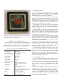
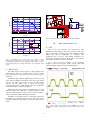
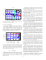
Contribution paper to the 7th Workshop on Electronics for LHC Experiments, 10-14, Sep. 2001, Stockholm.
Development and a SEU Test of a TDC LSI for the ATLAS Muon Detector
Yasuo Arai1, Yoshikazu Kurumisawa2 and Tsuneo Emura2
1
KEK, National High Energy Accelerator Research Organization,
Institute of Particle and Nuclear Studies, ([email protected])
2
Tokyo University of Agriculture and Technology
Abstract
A new TDC LSI (AMT-2) for the ATLAS Muon detector
has been developed. The AMT-2 chip is a successor of the
previous prototype chip (AMT-1). The design of the chip was
polished up for aiming mass production of 20,000 chips in
year 2002. Especially, power consumption of the chip was
reduced to less than half of the previous chip by introducing
newly developed LVDS receivers.
The AMT-2 was processed in a 0.3 µm CMOS Gate-Array
technology. It achieved 300 ps timing resolution and includes
several data buffers, trigger matching circuit, JTAG interface
and so on.
First SEU test by using a proton beam was recently
performed. Although the test results are very preliminary at
present stage, we get very low SEU rate safely used in
ATLAS environment.
In addition, the chip testability was enhanced. This is very
important for mass production. Mass production chips will be
mainly tested at LSI testes of the manufacturer. Only very
small fraction of the chip will be tested in our laboratory.
Since the LSI testers runs only at 10 MHz, special care must
be taken to verify 40 MHz operation. We think reduced
voltage test will certify the operation. To verify the stability of
the PLL, internal counter is prepared to count 80 MHz PLL
clock. After a fixed time, the counted value will be checked.
Photograph of the AMT-2 chip is shown in Fig. 2. The
chip is packaged in a 144 pins plastic (ceramic) QFP with 0.5
mm pin pitch. About 110k gates are used in a 6 mm by 6 mm
die.
The chip must be qualified to have adequate radiation
tolerance in ATLAS environment. Gamma-ray irradiation to
measure Total Ionization Damage (TID) was already done to
the same process [3]. Recently we executed a first experiment
of the Single Event Upset (SEU) test by using a proton beam.
Preliminary results are described in section IV.
I. INTRODUCTION
ATLAS precision muon tracker (MDT) requires highresolution, low-power and radiation-tolerant TDC LSIs
(called AMT: ATLAS Muon TDC). Total number of TDC
channels required is about 370 kch.
The AMT chip is developed in a 0.3 µm CMOS GateArray technology (TC220G, Toshiba Co.). Block diagram of
the chip is shown in Fig. 1. It contains 24 input channels, 256
words level 1 buffer, 8 words trigger FIFO and 64 words
readout FIFO. Both leading and trailing edge timings can be
recorded. The recorded data are matched to trigger signal
timing, and the matched data are transferred through 40 Mbps
serial line. By using an asymmetric ring oscillator [1] and a
Phase Locked Loop (PLL) circuit, it achieved 300 ps RMS
timing resolution.
A prototype chip, AMT-1, was successfully tested and
reported in the last LEB workshop [1]. Already 500 AMT-1
chips were produced and mounted in front-end PC boards
with ASD (Amp/Shaper/Discri) chips [2]. These boards are
being tested with MDT chambers in several laboratories.
AMT-2 chip is a successor of the AMT-1 chip and
regarded as a prototype for mass production. Major
improvement of the AMT-2 is reduced power consumption.
The AMT-1 consumes about 800 mW of which 470 mW is
consumed in LVDS receivers. We have developed a new lowpower LVDS receiver and proceeded to low power design of
logics. Thus the power consumption of the AMT-2 is reduced
to 360 mW.
-1-
Fig. 1 Block diagram of the AMT-2 chip.
A. AMT-2 Operation
The asymmetric ring oscillator produces a double
frequency clock (80 MHz) from a LHC beam clock (40MHz).
By dividing the 12.5 ns clock period into 16 intervals in the
oscillator, a time bin size of 0.78 ns is obtained.
A hit signal is used to store fine time and coarse time
measurement in individual channel buffers. The time of both
leading and trailing edge of the hit signal (or leading edge
time and pulse width) can be stored. Each channel has a 4word buffer where measurements are stored until they can be
written into the common level 1 (L1) buffer.
The L1 buffer is 256 hits deep and is written into like a
circular buffer. Reading from the buffer is random access
such that the trigger matching can search for data belonging to
the received triggers.
Trigger matching is performed as a time match between a
trigger time tag and the time measurements them selves. The
trigger time tag is taken from the trigger FIFO and the time
measurements are taken from the L1 buffer. Hits matching the
trigger are passed to the read-out FIFO.
Fig. 2 Open view of the AMT-2chip. The die size is about 6 mm by 6
mm. The photograph is ceramic packaged chip. Plastic packaged
ones are used in circuit tests and beam tests.
II. AMT-2 CIRCUIT DESCRIPTION
Main specification of the AMT-2 chip is summarized in
Table. 1. Since the detailed description of the AMT chip is
available in other documents [4, 5], only new features are
presented here after brief explanation of the chip operation.
Table. 1 AMT-2 Specification (@40MHz System Clock)
Least Time Count
Time Resolution
Dynamic range
Max. Trigger Latency
Int./Diff. Non Linearity
No. of Channels
Level 1Buffer
Read-out FIFO
Trigger FIFO
Double Hit Resolution
Hit Efficiency
Hit Input Level
Data output
CSR access
General I/O
Power
Process
Package
0.78125 ns/bit
300 ps RMS
13 (coarse) + 4 (fine) = 17 bit
16 bit (51 µsec)
< 80 ps RMS
24 Channels
256 words
64 words
8 words
<10 ns
100% @400 kHz (single edge)
>99.8%@400kHz(two edge)
LVDS
LVDS Serial (10 - 80 Mbps)
or 32 bit parallel.
JTAG or 12 bit control bus.
ASD control l (5 pins) and general out
(12 pin) and in (3 pin).
3.3+-0.3V, ~360 mW
0.3 µm CMOS Sea-of-Gate
144 pin plastic QFP
The data are transferred to a Chamber Service Module
(CSM) [6] through a serial data interface. The serial interface
supports both DS-protocol and simple data-clock output. The
data transfer speed is selectable between 10 MHz to 80 MHz
(40 MHz will be used in the MDT).
There are 15 control registers and 6 status registers. These
registers are accessible from JTAG interface. A total parity of
the control registers is stored in the status register. If a SEU
occurs in the control register, a parity error is caused and
notified through an Error signal or an Error packet.
The chip has JTAG boundary scan circuit, which is used
to scan I/O pins, the control and status registers, internal
circuit registers for debugging purpose, and BIST (Built-In
Self-Test) for the level 1 buffer and FIFOs. The channel
buffer and the level 1 buffer have a parity bit for each word to
detect SEU. In the AMT-2, ASD control function through the
JTAG is also added (see section II-C).
B. New LVDS Receiver
We used existing Toshiba design of the LVDS receiver in
the AMT-1. The power consumption of the LVDS receiver
(15.5 mW) does not cause much problem if the number of the
receiver is small. However we need 26 (30 in AMT-1)
receives, and the total power consumption becomes large
(470mW). Thus a new low-power LVDS receiver was
required.
Although the available transistor size is very limited in I/O
pad area in a Gate-Array, a low-power LVDS receiver was
successfully developed while keeping adequate performance.
Fig. 3 shows performance of the previous and new LVDS
receivers. The propagation time is even improved while
reducing the constant current. This was mainly achieved by
reducing the size of input transistors.
-2-
7
6
(a)
∆Vin=100mV
Old
Idd[mA]
5
4
3
2
New
1
0
0.0
0.5
1.0
1.5
Vicm[V]
2.0
2.5
6
Tpd[ns]
5
(b)
Fig. 4 ASD internal circuit and control signals from the AMT-2.
Old
4
Tpd(LH)
Tpd(HL)
3
III.
New
2
A. PLL
1
0
0.0
0.5
MEASUREMENT RESULTS
1.0
1.5
2.0
2.5
Vicm[V]
Fig. 3 Comparison of previous and new LVDS receiver
characteristics (simulation). (a) Constant current (Idd) vs. input
common mode voltage (Vicm), (b) propagation delay (Tpd) vs. Vicm.
LH and HL denotes Low to High and High to Low transition of the
output.
Jitter of the ring oscillator was measured by time
distribution between input clock edge and PLL clock edge
(Fig. 5). The jitter at operating point (3.3V, 80MHz) is 150 ps
RMS. This value is sufficiently low compared with
digitization error of 225 ps. Total timing resolution for a
single edge measurement will be about 300 ps. This satisfies
the required resolution of 0.5 ns in the MDT.
Fig. 6 shows the jitter variation to the oscillating
frequency (Fosc) and the power supply voltage (Vdd). This
indicates enough margins around the operating point.
C. ASD Control
The ASD chip has many registers to keep shaping time,
threshold DAC value etc. A Xilinx chip is used to control
these ASD registers from JTAG signal in the present frontend board.
This Xilinx chip consumes additional power and area, and
it also must be qualified for radiation. Since the power and the
area are very tight, it was decided to move the ASD control
function into the AMT-2. Fig. 4 shows the principle
connection between the AMT and the ASD. Five signal lines
are used between the ASD and the AMT-2.
Main protocol is almost same as JTAG boundary scan cell.
Data are shifted from ASDOUT to ASDIN through 3 ASD
chip. The shifted data are stored in shift cells and copied to
shadow cells when ASDLOAD signal is asserted.
In addition to the ASD control, 12 output and 3 input pins
are prepared as a general purpose I/O pins. These pins can be
used when additional control lines are needed in the front-end
board.
Fig. 5 PLL output clock (upper curve, 80MHz) and timing
distribution (histogram) triggered with external clock (lower curve,
40MHz).
-3-
Remaining issue is Single Event Effects (SEE) caused by
energetic hadrons (> 20 MeV) [7]. To measure the SEE, we
need to perform beam test to the chip.
Vdd[V]
2.5
300
2.7
2.9
3.1
3.3
3.5
3.7
3.9
There are several single event effects in which Single
Event Latch up (SEL) and Single Event Upset (SEU) are
important for CMOS process. We have done first test of SEU
by using a proton beam.
vs Fosc
vs Vdd
250
Jitter[ps]
200
We used an AVF cyclotron at the Cyclotron and
Radioisotope Center (CYRIC) of the Tohoku University,
Japan. The Cyclotron was recently upgraded and has
maximum proton energy of 90 MeV.
150
100
Operating Point
50
0
0
20
40
60
80
Fosc[MHz]
100
120
140
Fig. 6 PLL jitter variation for oscillating frequency (@Vdd=3.3V)
and supply voltage (@Fosc = 80 MHz).
B. Power Consumption
Total power consumption of the chip is measured at
several operating conditions and shown in Fig. 7. In a very
severe condition (100kHz hit rate and 100 kHz Trigger rate)
power consumption is about 15 mW/ch. Compared with
previous chip (AMT-1) we could reduce 18 mW/ch. This is
achieved mainly by using the new LVDS receiver and
reducing the number of LVDS receiver from 30 to 26.
40
AMT-2
100kHz Trig
100kHz Hit
Start
40MHz Clk
30MHz Clk
20MHz Clk
10MHz Clk
100 Ohm T
10
0
Fig. 7 Power consumption of the AMT-1 and the AMT-2 chips for
different operating conditions. Conditions are changed from left to
right; powered to LVDS circuit only, 100 ohm termination resistors
were connected to LVDS drivers, external clock (10-40 MHz) is
applied, measurement started, 100 kHz hit signals are applied, then
finally a 100kHz trigger signal is applied.
IV.
AMT-2 has 180 bits in the CSR registers, and a total of
11,360 bits in the L1, the trigger and the readout buffers. The
CSR register was composed of Flip-Flops, and the buffer
memories are composed of 6 transistors static memory cell.
Both circuits has almost complimentary circuit for positive
and negative logic signals, so we assume the SEU rate may be
same regardless of the contents of memory.
Unfortunately we cannot directly read and write the
contents of the buffers. Instead we used Built-in Self-Test
(BIST) circuit to detect the SEU. The BIST circuit performs
two kinds of 13N marching pattern test. The results are
compressed in a 36-bit Linear Feedback Shift Register. If one
or more error occurs in this test sequence, final result has
different value.
We step forward the BIST sequence until writing all '1's
(or '0's) to all memory location. Then irradiate the chip to the
beam. After the irradiation, we continue the BIST sequence
and read out the final value. These measurements were
repeated several times. Since the SEU rate is very low, it is
very rare to occur more than 2 SEU during one measurement.
We have observed 3 SEU in 18 measurements.
-18mW
20
LVDS Only
Power(mW/ch)
AMT-1
30
We have done a first beam test by using a 50 MeV proton
beam, and irradiated 2 AMT-2 chips. Beam intensity was
around 1 nA and the beam size was monitored visually to
have 2 cmφ. During the irradiation, beam intensity was
monitored with two plastic scintillators, but no special device
was used to measure its distribution.
SEU TEST
Radiation tolerance of the present process for Total
Ionization Damage (TID) was already measured and shows
adequate tolerance to gamma ray [3]. Furthermore CMOS
process is not sensitive to neutrons in estimated level of the
MDT environment.
As for the CSR, the contents are directly written and read
through JTAG lines. Before the irradiation '0's and '1's were
written to the CSRs, then after the irradiation the contents
were checked for SEU. We have not observed any bit flip in
the CSR test.
Fig. 8 shows leakage currents of the chip for gamma ray
and proton. Horizontal scale is adjusted to fit both curves.
Since the proton irradiation was paused during the
measurement, annealing was occurred during the each
measurement. Therefore the proton data are discontinuous at
the boundary of measurement. Assuming the leakage current
depend only on energy deposit in Si, proton flux is estimated
to be about 2x10⁹ protons/sec/cm2. This is consistent with the
value estimated from the beam intensity and its size.
The SEU test results are summarized in Table. 2.
Assuming a Poisson distribution of the SEU event, we get
upper limits of the cross section in 90% confidence level.
-4-
σSEU (CSR)
< 5.6x10⁻¹⁵ cm2/bit
V. SUMMARY
σSEU (buffer) < 2.7x10⁻¹⁶ cm2/bit
Calculated fluence of hadrons with an energy >20MeV is
~1010 1/cm2/10year in MDT location [7]. Applying number of
bit in total MDT system, SEU rates (RSEU) will be,
RSEU (CSR)
< 0.1 upset/day
A production prototype chip (AMT-2) was successfully
developed for ATLAS MDT detector. The chip fulfils
required performance and being tested with MDT chambers.
A new LVDS receiver is developed and the power
consumption of the AMT-2 chip is reduced to 45% of the
previous chip.
Preliminary test of SEU rate by using a proton beam was
performed and shows low enough rate to be safely used in the
MDT. Latch up was not observed in this test.
RSEU (buffer) < 0.3 upset/day.
Thus less than 1 upset in the CSR for 10 days of operation
in MDT system. Furthermore there was no latch up during the
experiments for both chips.
Although these results are very preliminary, we feel
relieved in very low SEU rate in both control registers and
data buffers. This is mainly because the transistor size is
relatively large in Gate-Array, so large charge is required to
upset the memory.
Although the leakage current was useful to estimate the
proton flux, but the large leakage current might cause damage
to the chip. Therefore it is better to irradiate less fluence to a
chip, and accumulate more statistics by irradiating many chips.
Further experiment are being planed.
300
0
250
100
Gamma Dose[krad]
200
Gamma Irrad.
(Upper Axis)
300
Annealing
Idd[mA]
200
Proton Irrad.
(Lower Axis)
150
100
12
1.4x10
50
0
0
200
400
600
2
protons/cm
800
1000
1200
Proton Irradiation time[sec]
Fig. 8 Leakage current of the AMT-2 chip for gamma ray and proton
irradiation. Data for proton is not continuous since the irradiation
was stopped in each measurements and annealing was occur in each
measurement.
VI.
I would like to thank to O. Umeda, I. Sakai, M. Takamoto,
K. Tsukamoto and T. Takada (Toshiba Co.) for their technical
support. I also thank to T. Shinozuka (CYRIC) who managed
to prepare beam time for us and M. Fujita (CYRIC) who gave
us many technical support for the beam test.
VII.
Chip 1
Chip 2
Chip 1+2
No. of
meas.
SEU
in CSR
SEU in
buffers
buffers
1.4x10¹²
1.0x10¹²
2.4x10¹²
8
10
18
0
0
0
1
2
3
6.3x10⁻¹⁷
1.8x10⁻¹⁶
1.1x10⁻¹⁶
REFERENCES
[1] Y. Arai and T. Emura, " Development of a 24 ch TDC LSI
for the ATLAS Muon Detector", Proceedings of the 6th
Workshop on Electronics for LHC Experiments,
CERN/LHC/2000-041, pp. 471-475.
[2] C. Posch, E. Hazen, and J. Oliver, "MDT-ASD, CMOS
front-end for ATLAS MDT", ATLAS Note, ATL-COMMUON-2001-019.
[3] Y. Arai, "Performance and Irradiation Tests of the 0.3 µm
CMOS TDC for the ATLAS MDT", Proceedings of the
Fifth Workshop on Electronics for LHC Experiments,
Snowmass, 1999. CERN/LHCC/99-33, pp 462-466.
[4] Y. Arai, "Development of Frontend Electronics and TDC
LSI for the ATLAS MDT", Nucl. Instr. Meth. A. Vol. 453,
pp. 365-371 (2000).
[5] ATLAS-Japan TDC group web page.
http://www-atlas.kek.jp/tdc/.
[6] CSM Design & User Manual,
http://atlas.physics.lsa.umich.edu/docushare/
[7] Atlas policy on radiation tolerant electronics.
http://www.cern.ch/Atlas/GROUPS/FRONTEND/radhard.
htm
Table. 2 Number of observed SEU in the proton irradiation
experiment.
Proton
Fluence
ACKNOWLEDGEMENTS
σSEU
-5-