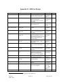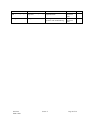
1
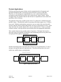
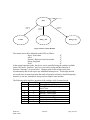
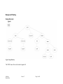
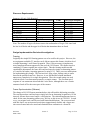
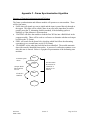
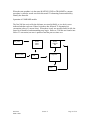
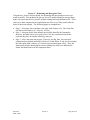
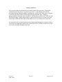
EE 552
Secure-T
Final Report
Ian Kuon - [email protected]
Mark Calder - [email protected]
November 27, 2000
Declaration of Original Content
The design elements of this project and report are entirely the original work of the authors
except as follows:
• 3-Way encryption algorithm was taken from Applied Cryptography [2]
• External Circuitry for LIU taken from CS63130 data sheet [5]
• Clock Divider Circuit taken from Student Application Note [11]
• The general model for the test bench has been taken from Lab 5 [12] and a student
application note [13]
• Source Code for 3-way encryption and cipher feedback mode operation taken from
Mcrypt[14]
____________________________
Ian Kuon
Date
Ian Kuon
Mark Calder
____________________________
Mark Calder
Date
Secure-T
Page 2 of 54
Abstract
This project is an undertaking to create a full duplex combination encryption
device and DS1 framer. The hardware receives the combined output from the 24
channels, encrypts this data using the 3-Way encryption algorithm in Cipher Feedback
Mode (CFB), assembles it into DS1 193S frame format, and then outputs this to a
standard Line Interface Unit (LIU) T1 interface chip, the CS61310. This data could then
be securely transmitted across any T1 line and the user at the other end could then use
another similar device to receive the data and decrypt it, provided they are aware of the
key. The project has been fully simulated and the results from simulation have been
compared to output from C/C++ programs that implement these algorithms. The
successful design was implemented on an Altera 10K20 FPGA found on an Altera UP1
board. This system was tested to verify complete functionality and the design was found
to operate correctly. The framing was found to be compliant by both a Super T1 ISA
card and a TauTron DS1 tester. Frame synchronization could also be found with these
sources. The encryption and decryption routines were also successfully implemented.
Ian Kuon
Mark Calder
Secure-T
Page 3 of 54
Table of Contents
Declaration of Original Content..................................................................................... 2
Abstract .......................................................................................................................... 3
Table of Contents ........................................................................................................... 4
Table of Figures ............................................................................................................. 6
Achievements.................................................................................................................. 7
Product Applications ...................................................................................................... 9
Description of Operation .............................................................................................. 10
Secure-T ...............................................................................................................................10
Encrypter .............................................................................................................................10
DS1 Framer ..........................................................................................................................12
Control Module ....................................................................................................................13
Clock Divider .......................................................................................................................15
Design and Testing....................................................................................................... 16
Design Hierarchy .................................................................................................................16
Resource Requirements .......................................................................................................17
Design Implementation Decisions/Investigations ................................................................17
Framing...........................................................................................................................................17
Frame Synchronization (Deframe)....................................................................................................17
Encryption/Decryption.....................................................................................................................19
Timing Investigations ......................................................................................................................19
Design Verification...............................................................................................................20
Testing Strategy for Frame Block .....................................................................................................20
Testing Strategy for Deframe Block .................................................................................................20
Testing Strategy for Encryption/Decryption......................................................................................21
Testing Strategy for Entire Secure-T Design.....................................................................................21
IC Characterization Results ......................................................................................... 23
Interface Testing ..................................................................................................................23
Functional Testing................................................................................................................23
References .................................................................................................................... 25
Appendix A – Product Data Sheet ................................................................................ 26
Part No. IM5434........................................................................................................... 27
Appendix B - LIU Datasheet ........................................................................................ 31
Appendix C - Frame Synchronization Algorithm......................................................... 34
Ian Kuon
Mark Calder
Secure-T
Page 4 of 54
Appendix D - Parts List ................................................................................................ 36
Appendix E - Simulation Results.................................................................................. 37
Test Case Index ....................................................................................................................37
Appendix F - Test Benches........................................................................................... 47
Appendix G - VHDL for Design ................................................................................... 48
Appendix H - C/C++ Source Code for Test benches .................................................... 50
Ian Kuon
Mark Calder
Secure-T
Page 5 of 54
Table of Figures
Figure 1 Duplex Mode.............................................................................................................................. 9
Figure 2 Single Operation Mode............................................................................................................... 9
Figure 3 Overview of Secure-T Structure .................................................................................................10
Figure 4 CFB Encryption ........................................................................................................................12
Figure 4 DS1 Framing Structure .............................................................................................................13
Figure 5 Secure-T State Machine.............................................................................................................14
Figure 6 Design Heirarchy......................................................................................................................16
Figure 7 Hardware Schematic .................................................................................................................30
Ian Kuon
Mark Calder
Secure-T
Page 6 of 54
Achievements
Framing
The framing module correctly outputs DS1 frames appropriate for use with the hardware
available. In simulation the correction operation was observed and this was confirmed in
hardware as both the DS1 tester and the Super T1 ISA card were able to find frame
synchronization with the output stream. This was accomplished despite a late change in
the framing format. It had been thought that the DS1 tester used DS1 frames since it was
not otherwise specified in the user manual; however, it was later determined that in fact
193S frames are used. This necessitated the late change to the newer frame format. Two
designs were made and tested for both original DS1 framing and Superframe D4 193S
frames; however, only the final 193S frame format was implemented on the chip since
the test equipment available is only able to work with this format. The proper
functioning of the framing module is a significant accomplishment since this exceeds the
intended goal of only implementing DS1 frames.
Frame Synchronization
The deframe module can find the frame bit of an incoming DS1 data stream and then
mark the frame bits with a signal. As such, it obtains synchronization with the incoming
data which allows operations such as encryption and decryption to be performed on the
data while not altering the framing structure. It can also pass the data through directly
without altering. As with the frame module the format was modified to 193S frames after
problems were discovered in communicating with the hardware. Thus two fully
functional modules with DS1 and D4 193S frames were implemented. Frame
synchronization is no simple feat and it is a considerable accomplishment to design a
system that can successfully find frame synchronization with a pseudo-random data
stream. Simulation verified the correct operation of this block and the hardware tests
supported this. The algorithm for frame synchronization is also noteworthy as it was
developed by the group. It provides quick and reasonably accurate detection of framed
signals while using a low number of logic cells and only a third of the ram on the chip.
Encryption/Decryption
A hardware design of the Three Way Encryption Algorithm in Cipher Feedback Mode
(CFB) was successfully completed. Simulation verified the output is correct by
comparing the output from a pseudo random stream of data to the expected output from
publicly available source code. This output could also be successfully decrypted. The
CFB operates in 1 bit block mode which allows synchronization without any alignment
signals. This is a powerful and required feature for a communications line since
alignment signals may not always be present as in the case of unframed data. The VHDL
implementation of the Cipher Feedback mode is flexible in that a different block cipher
could be used as a drop in replacement for the 3-way algorithm.
Ian Kuon
Mark Calder
Secure-T
Page 7 of 54
Space and time constraints prevented the design from implementing the typical 11 rounds
of the algorithm. The author of the algorithm allowed for any number of rounds; thus, it
was decided that one round would be implemented. It had been desired to allow for
arbitrary size Cipher Feedback Mode Encryption; however, size constraints prevented
this from being completed and tested.
As with the encryption, the publicly available Three Way Encryption algorithm was
implemented for decryption. Decryption was successfully implemented in a similar
manner to encryption.
The two blocks were successfully combined and fit to a usable size within the chip using
359 logic cells. This is a significant reduction from the number of blocks required for 8
bit CFB which exceeded the blocks available on the 10K20.
Secure-T
The blocks were successfully combined on a single Altera 10K20 device. Simulation
was successfully completed and it has been verified that the device functions correctly.
The design has also been successfully implemented in hardware on the UP1 board. The
device communicates with the T1 LIU on a separate board and is able to transmit and
receive data in full duplex operation.
It had been desired to include a method for entering the encryption key into the device
once programmed (during operation). With a 96 bit key, this is an arduous task using
switches and it was not possible to incorporate another interface to the chip such as a key
pad which would have made the task easier. Instead the key is determined when the
device is programmed. It can be easily changed via a single constant. This change has
the additional benefit that it prevents accidental altering of the key since it is unlikely that
the key will be changed while the device is in operation.
Ian Kuon
Mark Calder
Secure-T
Page 8 of 54
Product Applications
With the trend towards greater reliance on telecommunication for all corporate and
personal information, there is increasing concern about the security of this data.
Therefore, it is becoming more important that any voice or data transmissions be
encrypted to ensure that private data is only revealed to the “proper” parties. While
encryption does not guarantee that the data will not be compromised, it does reduce the
possibility of this occurring.
The solution to this privacy problem is the Secure-T, an innovative combined encrypter
and DS1 framer. This allows the traffic for an entire office that connects via a T1 line to
be secured. With the modern phone system one is never certain of the route the traffic
will take and this solution ensures that the data will not be compromised as easily. At the
other end of the line, another branch office can use another Secure-T chip or a possible
software solution, to decrypt the data, provided they know the appropriate information.
This versatile chip has many possible modes of operation. The digital side interface
allows the chip to be operated in full duplex mode transmitting and receiving data while
encrypting and decrypting as appropriate.
Backplane
Data
Secure-T
Cable /
Transmission
Network
T1 LIU
Figure 1 Duplex Mode
Another interesting mode of operation allows the device to be patched into a T1 line to
encrypt or decrypt the data in a single direction. This allows this product to be used
without any modification to existing boards.
Encryption or Decryption
T1 Line
T1 LIU
RX
Secure-T
T1 LIU
TX
T1 Line
Figure 2 Single Operation Mode
Ian Kuon
Mark Calder
Secure-T
Page 9 of 54
Description of Operation
The general structure of the chip is given in Figure 3.
Switches/
Buttons/
LEDs
User
Control
Backplane Data,
Frame Pulse and
Clock
Encrypter
RAM
Interface
T1 Framer
Controller
LIU
Control
Data/Clock to
and from LIU
1.544 MHz
Clock
Divider
Clock
24.704 MHz
Figure 3 Overview of Secure-T Structure
Secure-T
The top level entity provides the external connections along with the internal
interconnections. It allows for routing of the data based on the user selection of switches
on the UP1 board. This also produces the necessary clock and clock enable signals for
the blocks. Data is transmitted along with a clock in order for it to be correctly read in;
thus the function of Secure-T is to synchronize that clock with the appropriate internal
signals.
Encrypter
Encryption can be performed on the data to ensure that it is safely transmitted across
communication lines. Similarly decryption can be performed on the incoming data.
There are various algorithms available that perform encryption on binary data.1
The algorithm selected for this application is 3-Way. It is an unpatented algorithm
specifically designed to be hardware efficient and it provides more security than the Data
Encryption Standard (DES). It was selected over other algorithms such as IDEA because
1
Encryption or Decryption is accomplished by performing logical operations or permutations on the data stream so that the output no
longer appears to be related to the input stream. For an in depth discussion of encryption techniques and reasons for performing
encryption refer to Applied Cryptography [2].
Ian Kuon
Mark Calder
Secure-T
Page 10 of 54
of space constraints on the chip. It was required to select an algorithm that did not
require look up tables since the RAM on the chip was reserved for use with the frame and
frame synchronization procedures. The algorithm has been publicly available since 1995
and has had no known successful cryptoanalysis against it.2
The 3-way algorithm that is implemented in this block is as follows
For i = 0 to n -1
x = x ⊕ Ki
x = theta (x)
x = pi -1 (x)
x = gamma (x)
x = pi - 2 (x)
x = x ⊕ Kn
x = theta (x)
where
n is the number of rounds
theta (x) is a linear substitution function
pi-1 (x) and pi-2 (x) are permutations
gamma(x) is a non linear substitution function3
The bit order of the data must be reversed for decryption; however, because Cipher
Feedback will be used as discussed below, it will not be necessary to perform decryption
and the block cipher itself will always be used in encryption mode.
This block will implement the encryption using the Cipher Feedback Mode (CFB) which
will effectively make this algorithm behave as a self synchronizing stream cipher. Selfsynchronization is important to this application since there might be no other way to
synchronize the codes and correctly decrypt the information. An overview of CFB mode
is given in the diagram below. Decryption in CFB mode is accomplished by changing
the positions of the plain text and the cipher text in the XOR operation. The cipher text is
used in the register.
2
3
Schneier, Bruce. Applied Cryptography. John Wiley & Sons Inc. Pg. 342
Schneier, Bruce. Applied Cryptography. John Wiley & Sons Inc. Pg. 342
Ian Kuon
Mark Calder
Secure-T
Page 11 of 54
Last 12 bytes
3-Way
Encryption
Key
96 bit cipher outputi
Least Significant Block of
Cipher Text
plaintexti
ciphertexti
Figure 4 CFB Encryption4
This approach requires an initialization vector (IV). This code is only required at the start
of each message. Since the T1 data is a continuous stream of data this must only be
performed once on power up. The device can then continue operating indefinitely
without an IV. This same IV is used for decryption and encryption. Since the IV is
essentially not required except for power up, it was decided that a single constant IV
would be used. While in theory, the IV should be unique, it was not considered
significant enough to warrant the significant additional logic this would have required.
Furthermore, synchronization of the IV between encryption and decryption at the two
ends of a T1 line would prove to be difficult. If frequent power cycling occurs, making
the weak IV a concern, a future version of the device could allow for a random IV.
Although, without synchronization this will mean that the first 96 bits will be lost.
With data transmission there is a the potential for bit errors. When they occur a single bit
error will impact the following 96 bits as well due to the CFB mode of operation. While
this is a significant loss, the requirement for self synchronization forced the choice of this
mode.
DS1 Framer
A frame is a large data structure that contains signaling and data bits so that the data may
be properly handled. For this design the DS1 frame format, which runs at a speed of
1.544 Mbit/s and is widely used for network communication among offices, will be used.
The T1 carrier frame that will be implemented is the North American version using 24
channels as opposed to the 32 channels used by the European version. Framing is
4
Schneier, Bruce. Applied Cryptography. John Wiley & Sons Inc. Pg. 200
Ian Kuon
Mark Calder
Secure-T
Page 12 of 54
required in order to preserve the alignment of these different channels so that the
individual channels can be processed as required.
The encrypted data will be passed to the framer which will put the data in the appropriate
format. The framer will also be capable of taking framed data and synchronizing with it
so that each of the channels can be properly identified.
There are numerous types of framing DS1 structures possible. The simplest format is
DS1 framing. For this format the 24 channels, with 8 bits each, are combined in the T1
line and a framing bit is inserted at the beginning, giving a total of 193 bits per frame.
The framing bit alternates between 0 and 1 to ensure frame alignment. Some
implementations use data robbing whereby some data bits are used for signally; however,
this framer will not use bit robbing to send control information as this chip is intended to
be used with data as well.
Frame
1 Bit
Channel 1
8 bits
Channel 2
8 bits
Channel 3
8 bits
…
Channel 24
8 bits
Figure 4 DS1 Framing Structure5
This design was successfully implemented; however, it was decided that to increase the
versatility of the device, the more commonly used D4193S Super Frame Format would
be used. This structure groups the single DS1 frames into a 12 Frame structure known as
a super frame. The following bit pattern is then used in the frame bits. "100011011100".6
The framing process for the data is fairly straightforward; however, the algorithm for
frame synchronization is more complex. Frame synchronization will be found using a
parallel algorithm. It stores the first frame received and compares each of the bits in this
frame to the next frames until only one possible candidate for the frame bit remains. A
synchronization signal is produced to indicate that alignment has been found correctly.
Frame pulses are then produced to indicate the position of the frame bit in the data
stream. For a detailed overview of the algorithm that will be used please refer to
Appendix C.
Control Module
The user will be able to interface with the chip using the switches and push buttons.
There will be a reset button that will put the chip in its initial operating mode. The status
of the chip will be shown using various LEDs. The Secure-T has full duplex
functionality allowing data to be encrypted and framed at the same time as decryption
and frame synchronization is occurring.
The following state machine provides an overview of the operation of the machine.
5
Fort Hays State University. INT 478 B Datacom Chapter 8. Internet. 2000.
http://int.fhsu.edu/kevin/courses/datacom1/html/chapter_8.html
6
Super-T1 Card User's Guide. GL Communications. Pg A-1.
Ian Kuon
Mark Calder
Secure-T
Page 13 of 54
Reset=0
Reset
Switch=0
Enter=0
Normal
Switch=1
Enter=0
Switch=2
Enter=0
Debug _All1
Debug_Loop
Figure 5 Secure-T State Machine
The current state will be indicated on the LEDs as follows.
Reset - Reset State
“0”
All1's
“1”
Normal - Behavior based on switches
“2”
Debug Loopback
“3”
Error
“8”
In the normal operation mode, the device can be controlled using the switches available
on the UP1 board. Switches 1 and 2 are reserved for testing and the functions of
Switches 3 through 7 are given below. Changes made on the switches take place
asynchronously and do not require any additional button presses. This design decision
was made since in normal operation the mode of operation will not be altered frequently;
therefore, it was not warranted to design a more complex state machine.
The following table describes operation of the switches while in normal mode.
Switch Control_Bit
Description
1
0
Debug Mode –All1 – Active Low
2
1
Debug Mode – Device Loopback –
Active Low
3
2
Encrypt – Active High
4
3
Decrypt – Active High
5
4
Frame – Active High
6
5
Deframe – Active High
7
6
Loopback – Active High
8
7
Reserved
Ian Kuon
Mark Calder
Secure-T
Page 14 of 54
Clock Divider
T1 protocol operates at a speed of 1.544 Mbit/s; thus it will be necessary to have a clock
of this frequency available so that the data can be properly output. As well, the LIU
requires a T1 speed clock for it to function correctly. However, for many operations, in
particular the encryption and frame synchronization blocks, it will be desirable to have a
higher speed clock and thus, a higher speed will be given to the chip. This block divides
the device clock (24.704 MHz) by 16 to produce a T1 speed (1.544 MHz) signal. An
enable signal is also provided for internal blocks. The enable signal only pulses high for
1 clock cycle.
Ian Kuon
Mark Calder
Secure-T
Page 15 of 54
Design and Testing
Design Hierarchy
Figure 6 Design Heirarchy
The VHDL Source files can be found in Appendix G
Ian Kuon
Mark Calder
Secure-T
Page 16 of 54
Resource Requirements
Summary of Logic Cells Required
Logic Cells Required
frame
279
deframe
154
compare
107
frameblock
428
cfb_encrypt
178
cfb_decrypt
180
encrypt
359
divide_clock
7
Total for Secure-T
798/1152
EABs
2
2
2
4
0
0
0
0
4/6
Max Clock Frequency
24.05 MHz
35.46 MHz
36.63 MHz
30.00 MHz
25.64 MHz
103.9 MHz
29.67 MHz
113.63 MHz
24.03 MHz
Note: The number of logic cells do not sum to the total number of Logic Cells since both
the low level blocks and the upper level blocks that instantiate them are listed.
Design Implementation Decisions/Investigations
Framing
Originally the simple DS1 framing pattern was to be used for this project. However, the
test equipment available (T1 interface card), did not support this format, which involved
a simple alternating 1 and 0 frame bit pattern. Thus, it was necessary to implement a
more complicated format supported by the card, the 193S format. This format involves
combining 12 frames together into a super frame. Thus the framing module needed
considerable adjustments, the frame bit would no longer be simply an alternating pattern
of 1s and 0s, but rather a repeating pattern of a string of 12. There were two main options
for implementing this change. The first involved using a lpm_shiftreg entity to rotate
between the possible frame bits. However, it was felt that this solution introduced
unnecessary complexity for a single bit operation. Thus, the second option was used
which involved a case statement operated by a simple counter. The excellent speed
response of case statements also made this a wise choice, although there was a certain
amount of trade off for the extra space of the counter.
Frame Synchronization (Deframe)
The change to D4 193S format mentioned above also affected the deframing procedure.
The search procedure could no longer simply look for an alternating bit pattern in 193 bit
intervals, because that was no longer a valid criterion. The solution implemented was to
check for the same alternating pattern every 386 bits, as this is true in 193S DS1. In such
a way, our original code could be used with limited modifications. The cost associated
with this choice was an increased search time (approximately double) and a larger area
since more frames had to be stored and eliminated from contention as a frame bit.
Ian Kuon
Mark Calder
Secure-T
Page 17 of 54
The frame synchronization algorithm used a parallel frame bit search strategy, as opposed
to a serial strategy (for more details on the frame synchronization algorithm see
Appendix C). The parallel scheme involves looking at every bit as it enters and
determining if it is an eligible frame bit. When only one bit is left eligible, the frame bit
is found. A serial search scheme would involve looking at a particular bit index within
the frame until that bit did not fit the framing convention, then moving to the next bit. If
a bit kept framing convention for a set period of time it would be found to be the frame
bit. The advantage to this scheme is it can be implemented in less logic cells, as one does
not need to store the current eligibility of each of the bits. However, in the average case
it is far slower than the parallel algorithm, since several frames of data may pass by as
each non-frame bit is cycled through. It also leads to a greater chance of error if a
random data bit follows framing convention for a period of time. Thus, the parallel
scheme was used. To deal with the greater storage size, a RAM block (implemented with
EAB’s) was used to keep track of the eligibility of each block.
In order to minimize chip area (logic cell count) it was determined that storage of the
vectors required for determining frame synchronization would be done using RAM.
Numerous different trials have been performed using the LPM modules for the interface
to RAM. First the design was implemented using the lpm_ram_dp modules; however,
compiling this approach indicated that no EAB's (i.e. no RAM) was being used and
instead it was implemented in logic cells which led to an excessively large design. The
Dual Port module had the functionality desired however, this implementation with Logic
Cells was not acceptable. The design has therefore been changed to use lpm_ram_dq.
The 193 check bits stored in RAM and used in the Compare module was implemented
using lpm_ram_dq instead of lpm_fifo. Initially it was desired to implement using
lpm_fifo, as this would allow us to both pull a value from RAM and store a new value in
RAM simultaneously. However, implementing with lpm_fifo led to the total logic cells
used (at the time) to increase from around 225 to 550, and the number of EABs to
increase to 3. By pulling from the RAM during the first half of the clock cycle, and
inserting in the second half of the clock cycle we managed to attain the same
functionality of the lpm_fifo with the lpm_ram_dq.
Initially the deframe module used a lpm_fifo structure to store data when the chip was
attempting to find synchronisation with the input stream. This data could then be output
with the frame bit correctly identified once the synchronisation has been found.
However, this structure used 2 EABs and a large number (roughly 150 logic cells) to
implement. Also, the size of the lpm_fifo component would have to be fairly large to
store all of the necessary data (in an average case it would take 9 frames of data or 3474
bits to identify the frame bit)7. For these reasons, it was decided to simply pass through
the beginning frames of data until synchronisation is found.
7
The average case is calculated with the assumption that half of the bits will be eliminated from frame bit
eligibility each frame. Hence, one will need log2(386) frames, or approximately 9 frames of size 386 bits.
Ian Kuon
Mark Calder
Secure-T
Page 18 of 54
Encryption/Decryption
The encryption algorithm was initially implemented and found to be too large for the
intended device, requiring almost 1000 logic cells, leaving nothing for any other
functions. To remedy this problem, the CFB block size was varied. This was found to
have a significant effect on the size of the implementation. Therefore, it was decided that
a 1 bit block will be used. This gives the greatest flexibility for a self-synchronizing
stream cipher as there is no alignment that must be determined. Initially, the intent was
for an 8 bit CFB (1 byte) block which would have allowed for easy comparison with
standard available CFB encryption libraries such as Mcrypt. Unfortunately this change
meant that slight modifications to the standard encryption schemes were required. This is
not a significant problem as the data is still adequately encrypted and can be decrypted by
a software algorithm or another Secure-T device. It had been initially desired to vary the
number of rounds used in the encryption process; however, this proved difficult to
accomplish in the allotted time. As well it was feared that such a modification would
increase the size of the design beyond the capacity of the chip. Therefore it was decided
to have the design only perform one round of encryption. While the impact of this
change to the security of the algorithm is unknown, it was considered worthwhile given
the savings in area and design time it provided.
While the encryption routines all passed in the test bench simulations, it was found later
during top level simulations that a timing problem in the CFB encryption routine
prevented data from being transmitted to the other blocks in the chip. This problem was
corrected by adding a register on the outputs from the encryption and decryption blocks.
Once this correction was implemented all the blocks simulated correctly.
Timing Investigations
In combining the various blocks (frameblock and encrypt) it was realised that it would be
necessary to minimize any timing delays as the design is relatively large. One approach
used to accomplish this was the use of ranges on any natural or integer signals in the
design. During the initial design phases all the integers and naturals were left with
default ranges and this was found to produce blocks with relatively slow minimum clock
periods. In particular the framing block was found to improve from a maximum clock
frequency of 12.67 MHz to 23.75 MHz when the range of values was limited to the actual
required range. This speed up was significant since it allowed the frame block to operate
at full speed.
The interconnection of the blocks in the Secure-T entity was considered low risk;
however, after completion it was found that the timing constraints of the large design
prevented it from operating correctly according to the Timing Analyzer of Maxplus2.
Numerous errors similar to the following were found to occur
Error: Delay path from
'|encrypt:encrypt_Block|Tway_cfb_encrypt:encryption_d
evice|LPM_SHIFTREG:output_shift_reg|dffs74.q' to
'|encrypt:encrypt_block|Tway_cfb_encrypt:encryption_d
evice|LPM_SHIFTREG:output_shift_reg|dffs74.Q'
Ian Kuon
Mark Calder
Secure-T
Page 19 of 54
is 5.1ns but Clock skew is 3.5 ns and hold time
required for
'|encrypt:encrypt_block|Tway_cfb_encrypt:encryption_d
evice|LPM_SHIFTREG:output_shift_reg|dffs75.Q'
is 1.6ns -- circuit cannot operate because Clock skew
plus hold time of destination register exceeds
register-to-register delay
This was despite the fact that all the blocks had been successfully checked as they were
designed. To resolve this problem varying the Speed vs. Area slider was attempted
which was able to remove some of the areas; however, errors still occurred and slight
changes in any logic caused the location of these errors to move preventing one from
specifying a specific timing constraint. A newer version of Maxplus2 was used without
success at solving this problem. It was eventually found that a fixing a minor bug in one
of the blocks removed this error; however, the reason for this is not clear as the change
was not on one of the erroneous blocks. This error is a significant concern and should it
occur again it is unknown what can be done to eliminate it.
Design Verification
The strategies that were used for testing are discussed below. The simulated waveforms
and the output from the test benches that verify these tests pass can be found in the
Appendix.
Testing Strategy for Frame Block
A test bench was used to ensure the correct operation of the framing block. It read input
values from an input file along with the expected output. This expected output was then
compared to the actual data produced by the frame block. The values in the input files
were generated by a C program that produces data testing several cases using pseudorandom data. The C program will produce the correct framed results and output both
these and the inputs to files. Listed below are the cases that were tested:
•
•
•
Base Case #1: Data is all zeros. The output data should also be all zeros with the
exception of a varying frame bit every 193 bits.
Base Case #2: Data is all ones. The output data should also be all ones with the
exception of a varying frame bit every 193 bits.
Case #3: Random data. This data will be generated using the rand function. The
output should preserve the input data with the correct alternating frame bits every 193
bits.
The successful passing of these tests indicates that the frame block functions correctly.
Testing Strategy for Deframe Block
Ian Kuon
Mark Calder
Secure-T
Page 20 of 54
A similar procedure to that used for the Frame Block was used. A test bench once again
read input and output values from files to ascertain correct operation. Once again a C
program was used to produce these input and output files. Listed below are the cases that
were tested:
•
•
•
•
•
Base Case #1: Data is all zeros except for frame bits. The output data should be all
zeros.
Base Case #2: Data is all ones except for frame bits. The output data should be all
ones.
Random Case: Data will be produced using the rand function. This will simulate the
average case.
Worst Case: Data will be picked so as all bits follow the T1 format for a relatively
large amount of time. This is the most difficult for the deframe block to detect.
Error Case: Data that does not include an accurate frame bit will be produced. The
deframe block should detect the error and produce an error message before resetting.
Frame synchronization should again be found once the correct data is again passed
These cases should prove sufficient to satisfy in terms of correct deframe block operation.
Testing Strategy for Encryption/Decryption
As there are standard C programs available that perform the encryption and decryption
algorithms these programs were used on pseudo random data to generate a data stream
that can be compared to the output of the Encryption and Decryption blocks. The tests
were performed on various key combinations. Any deviations from expected results
were flagged with a test bench. Given the length of the simulation time, waveform
simulation is not particularly informative. Instead, the VHDL for the test bench has been
included as well as the C code for generating the data. A sample page from the test
bench output can be found in the Appendices.
The basic 3 way cipher block was tested independently as well to ensure that this
implementation is correct since it is critical to the operation of all the other blocks. This
can only be done on a select few cases as it was found that the test bench conversion
procedures are not capable of handling 96 bit vectors. Thus, this is done manually in
Mentor Graphics.
Testing Strategy for Entire Secure-T Design
A test bench will be used to ensure the correct operation of the entire chip. The data from
the chip will be compared to the expected data which will be taken from standard or
custom C programs. The chip will be tested in the following modes
• No encryption - verifies correct operation of the frame/deframe circuitry
• Encryption with Framing - verifies correct operation of the frame and encrypt
Ian Kuon
Mark Calder
Secure-T
Page 21 of 54
•
Decryption with Frame Synchronization - verifies correct operation of deframe and
decrypt.
A complete listing of the test cases along with the sample output waveforms or test bench
data can be found in the Appendices.
Ian Kuon
Mark Calder
Secure-T
Page 22 of 54
IC Characterization Results
Interface Testing
For testing the functionality of the T1 LIU, two debug modes allow the Secure-T chip to
force the T1 LIU into all 1's(TAOS) or remote loopback (RLOOP) mode. Testing of this
stage was considered complete when there are no bit errors in loopback mode using the
DS1 Tester. This test has been successfully completed. Framed and Unframed data of
any type were successfully looped through the CS61310.
Loopback through the Secure-T was then performed with limited success.
Inconsistencies in the operation of the Line Interface unit caused some significant
problems. Investigation has revealed that in some circumstances not specified in the Data
sheet the device enters a Receiver Power Off mode. In this state the receiver outputs no
data making testing difficult. Technical support for Cirrus Logic (the manufacturer of the
LIU) has been contacted; however, no suitable advice has been obtained. It has been
possible to get the receiver to function in some cases and on those occasions loopback
through the Secure-T occurred; however, some bit errors were found to occur. This is
likely due to noise on the board and in between the UP1 board and the T1 LIU. These bit
errors are a concern and the wires will be made as short as possible in an attempt to
minimize this. However, since the general operation is confirmed, this test will be
considered a pass
Functional Testing
DS1 Framing
The framing will be tested via the Super T1 ISA card and the DS1 Data generator.
Sending an all 1’s data pattern into the Secure-T yielded an output to the LIU (on
LIU_data_tx) that was high except for occasional low pulses that are frame pulses. The
correct frame formatting was confirmed by sending this data into the T1 ISA card in
Monitor mode. This mode checks for any errors in the data received by the card. Over
an extended period of time no bit errors were observed and frame synchronization was
maintained. On four separate occasions over a period of ½ hour, fewer than 5 frame bit
errors were observed. This successfully proves that the design of frame is correct. For
completeness this should be tested on multiple patterns; however, the SecureT lacks a
data generator for performing this test. A future version of this device may include this
feature; however, based on the design of the frame module, it is highly unlikely that the
contents of the data will impact the frame transmission. Therefore, the operation of
frame can be considered correct.
Encryption/Decryption
The encryption algorithm was tested by sourcing all 1’s data into the dig_data_in. This
all ones pattern was encrypted and captured on the PC using the ISA card.
Ian Kuon
Mark Calder
Secure-T
Page 23 of 54
Unfortunately, the format of the file is not readable by any common utilities and therefore
this could not be properly verified. The output data is clearly being altered from the all
1’s pattern so it is obvious that the encryption is somewhat functional. Since the
simulation demonstrated that encrypt functions correctly and there were no critical timing
problems in this module, one can be reasonably assured that the functionality is correct
on the chip. Therefore, this encryption implementation will be considered to be a
conditional pass.
The decryption routine was tested in a similar manner except the chip was set in loopback
mode. Again the inability to read the file has prevented the gathering of conclusive
evidence that the decryption is fully functional. The algorithm was correct in simulation,
though, and thus this test will be given a conditional pass.
Frame Synchronization
The Frame Synchronization routine was verified using the DS1 tester and the Super T1
Card. First it was verified that frame synchronization could be found with e 193S framed
stream of data. Once frame synchronization was found it was indicated via an LED.
This was found to occur in some occasions; however, the difficulties with the T1 LIU
receiver made conclusive tests difficult. The LED was found to light up in response to
framed data and once the source is removed the light would turn off. This is the desired
response and indicates that the deframe module can function correctly. This will be
considered a conditional pass.
Ian Kuon
Mark Calder
Secure-T
Page 24 of 54
References
[1] Katzan, Harry Jr. The Standard Encryption Algorithm. Petrocelli Books, 1977 United
States.
[2] Schneier, Bruce. Applied Cryptography Protocols, Algorithms, and Source Code in C.
John Wiley & Sons Inc. 1996. Toronto.
[3] Black, Uyless. Computer Networks (Protocols, Standards, and Interfaces). Prentice
Hall, 1987 Englewood Cliffs, New Jersey.
[5] Dallas Semiconductor. DS2148 Datasheet. Internet. 2000.
http://www.dalsemi.com/datasheets/pdfs/2148.pdf
[6] Fort Hays State University. INT 478 B Datacom Chapter 8. Internet. 2000.
http://int.fhsu.edu/kevin/courses/datacom1/html/chapter_8.html
[7] Cirrus Logic. CS61310: Long Haul T1 Line Interface Unit. Internet. 2000.
http://www.cirrus.com/design/products/overview/index.cfm?ProductID=99
[8] Caplan, Stephen, et al. E-safe. Internet. 2000.
http://www.ee.ualberta.ca/~elliott/ee552/projects/1998f/esafe/
[9] Au, Jodie, et al. SafeTalk. Internet. 2000.
http://www.ee.ualberta.ca/~elliott/ee552/projects/1999f/SafeTalk/FinalReport.pdf
[10] Dayton, Robert L. Guide to Integrating Digital Services: T1, DDS, and Voice
Integrated Network Architecture. McGraw-Hill Book Company. New York, NY. 1989.
[11] Leder, Daniel. Clock-Dividing using Carry-Save and Determining Carry-Save
Counter Outputs. Internet. 2000.
http://www.ee.ualberta.ca/~elliott/ee552/studentAppNotes/1999f/clock_divider/.
[12] Koob, John and Sung, Raymond. Adder Test Bench. Internet. 2000.
http://www.ee.ualberta.ca/~elliott/ee552/labs/adder_test.vhd.
[13] Gunthrope, Jason, et al. TestBenches Using File I/O under VHDL. Internet. 2000.
http://www.ee.ualberta.ca/~elliott/ee552/studentAppNotes/2000_w/vhdl/File_IO_Testben
ching/testbench.html
[14] Mavroyanopoulos, Nikos. Mcrypt. Internet. 2000. http://mcrypt.hellug.gr/
[15] Super T1 User’s Manual. GL Communications. 1995. United States.
Ian Kuon
Mark Calder
Secure-T
Page 25 of 54
Appendix A – Product Data Sheet
Ian Kuon
Mark Calder
Secure-T
Page 26 of 54
Part No. IM5434
Secure-T – Combined Encryption Device and DS1 Framer
Product Data Sheet
Features
• Connects seamlessly to T1 Line Interface Unit CS61310
• Provides Full Duplex Cipher Feedback mode encryption and decryption using the
Threeway Block Cipher Algorithm
• Encryption Algorithm is self synchronizing and requires no alignment information yet
will still operate correctly when frame information is provided
• Finds Frame Synchronization with a 193S framed signal
• Frames data according to D4 193S Superframe format.
• Capable of operating in Digital Loopback mode and still providing encryption or
decryption functionality
• Can be set to transmits Alarm Indication Signal (AIS) or operate in loopback mode.
• Requires only a single 24.704 MHz clock
• State Information is provided via a 7 segment display
• Frame Synchronization is indicated via an LED and will typically be found within 1
ms
Description
The Secure-T is a combined T1 framer and encryption device. It interfaces with a T1 line
interface unit to provide full duplex transmission of recovered T1 or backplane data with
unframed DS1 data and unencrypted or encrypted data. The encryption algorithm
operates in single bit Cipher Feedback mode which allows self synchronization with any
bit stream.
Modes of Operations
The Secure-T will power up in Reset “0” Mode. To ensure normal operation, clear
should be pressed after power up. Normal Operation, Status “2” will begin when enter is
pressed and Switches 0 and 1 are high. Once in Normal Operation Switches 2 through 7
determine the routing of the data and determined the processing of the data (i.e framed,
encrypted, etc.)
Switch
0
1
2
3
4
Ian Kuon
Mark Calder
Control
Debug Must be 1 for Proper Operation
Debug Must be 1 for Proper Operation
Encrypt Enable – Active High
Decrypt Enable – Active High
Frame Enable – Active High
Secure-T
Page 27 of 54
5
Framing Synchronization Enable –
Active High
Loopback Enable – Active High
Reserved for Future Use
6
7
System Wide Active Low Clear resets all the registers in the Secure-T.
LED Status
Display Display
A
B
X
0
X
8
X
1
X
3
X
2
2
Status
Reset
Error
Debug State – Not Intended for Regular Operation
Debug State – Not Intended for Regular Operation
Normal Operation
Normal Operation – Frame Synchronization Found
Pin Descriptions
Pin Name
clock
clear
enter
LED_Segment_a(6 downto 0)
LED_Segment_b(6 downto 0)
switches(7 downto 0)
dig_data_in
dig_in_fp
dig_in_clk
dig_data_out
dig_out_fp
dig_out_clk
liu_data_RX
Ian Kuon
Mark Calder
Pin
Pin
Function
Direction
Number
Control Signals
Input
45
System Clock - 24.704 MHz
Input
28
Active Low Reset Signal
Input
29
User Input Control
Output
6, 7, 8, 9,
LED Segment A of UP1 Board
11, 12, 13
Output
17, 18, 19,
LED Segment B of UP1 Board
20, 21, 23,
24
Input
41, 40, 39,
Input Switches
38, 36, 35,
34, 33
Backplane Data Signals
Input
48
Backplane Digital PCM data to be sent
Input
75
Backplane Frame Pulse Data
Input
73
Backplane 1.544 MHz Clock for Data
Output
100
Backplane Digital PCM data recovered
from T1 Line
Output
84
Backplane Frame Pulse Data recovered
from T1 Line
Output
80
Backplane 1.544 MHz Clock for Data
LIU Data Signals
Input
55
T1 Data recovered from T1 line by
Secure-T
Page 28 of 54
RX_Clock_in
liu_data_TX
Tx_Clk_Out
clk1544
rloop
lloop
taos
los
LIU
T1 Clock from RX of LIU
T1 Data to be sent to the LIU
T1 Clock for TX to LIU
Input
Input
Output
54
61
51
LIU Control Signals
Output
53
Slow Clock for use as master clock on
T1 LIU
Output
70
RLOOP of CS61310
Output
63
LLOOP of CS61310
Output
72
TAOS of CS61310
Input
65
LOS from CS61310
Implementation Information
The design is intended for use with the Altera EPF10K20. The sof file for programming
the device is available.
Logic Cells Used
Recommended Frequency of Operation
798/1152 = 69.4%
24.704 MHz
Timing Information
Only Typical Values are available since no IC Test equipment was available to measure
the delays. The most significant delay times guaranteed only by simulation are given
below
Tp clk-clk1544
22.3 ns
Tp clk-TAOS
25.6 ns
Tp clk-RLOOP
22.4 ns
Tp clk-Dig_data_out 30.9 ns
Tp clk-Dig_out_fp
24.0 ns
Tp clk-Liu_data_TX 22.3 ns
Electrical Information
For detailed electrical information please refer to the Altera Data sheet for the
EPF10K20RC240-4.
Interface
A schematic describing all the required connections is given below. This circuitry has
been built on a separate board that will be connected to the UP1 board. A datasheet for
the CS61310 is provided in Appendix B.
Ian Kuon
Mark Calder
Secure-T
Page 29 of 54
Figure 7 Hardware Schematic
Ian Kuon
Mark Calder
Secure-T
Page 30 of 54
Appendix B - LIU Datasheet
Selected Pages of the data sheet for the CS61310 are attached.
Ian Kuon
Mark Calder
Secure-T
Page 31 of 54
Ian Kuon
Mark Calder
Secure-T
Page 32 of 54
Ian Kuon
Mark Calder
Secure-T
Page 33 of 54
Appendix C - Frame Synchronization Algorithm
Structure of Framing Synchronization and Deframer
The frame synchronization and deframe module will operate as a state machine. There
will be four states:
• PASS where all signals are reset to initial and the input is passed directly through to
the output. This state will be called if there is an error in the input data (it can not
possibly meet the T1 alternating lead bit standard), if the deframing option is
disabled, or if the deframer is first turned on.
• WAITING will allow the module to load the first 385 bits into a RAM block in the
compare module. These will be used as a reference to determine whether each input
bit follows the T1 format.
• FIND, will search for the frame bit by checking which bits follow the alternating
convention (every second frame as per S193 format).
• TRANSMIT occurs when the frame bit has been identified. The module transmits
data with correctly identified frame pulses. A process of verification continues even
after this state is entered. Below is a graphical representation of the deframing state
machine:
PASS
If deframe option
chosen.
WAITING
Compare RAM
filled with first
193 bits.
If lead bit is
identified.
If no bits match
the criterion for
a frame bit or
deframe is not
selected.
FIND
TRANSMIT
Ian Kuon
Mark Calder
Secure-T
Page 34 of 54
When the state machine is in the states WAITING, FIND or TRANSMIT a compare
procedure is called to search out which bits match T1 alternating format and thereby
identify the frame bit.
Operation of COMPARE module
The first 386 bits received by the deframer are stored in RAM, as is a check vector
indicated whether each one of these bit indexes has followed T1 alternating bit
convention (value of 1 means it has.) When there is only one possible frame bit left, the
frame bit is identified, and transmitting may begin. However, if all bits are found to not
follow T1 convention, an error is produced and the process starts over.
Bit_index
Same_value
RAM
initial
frame
RAM
CHECK
bits
Comparator
XOR
AND
Ian Kuon
Mark Calder
Secure-T
Page 35 of 54
Appendix D - Parts List
Quantity
Part
1
1
1
UP1 Board with FLEX10K20
CS61310
24.704 MHz Clock Oscillator
1
1.544 MHz Clock Oscillator (For
testing)
33 µF capacitors
1.0 µF capacitors
0.1 µF capacitors
0.47 µF capacitors
50 Ω resistors
9.1 Ω resistors
1:1 Transformer with Centre Tap
1:2 Transformer
T1 Cabling
Header Board
wire for connections
1
1
1
2
2
2
1
1
Ian Kuon
Mark Calder
Part Number if
Applicable
Secure-T
CS61310
300-8020-1ND
SE1216-ND
257-1008-ND
257-1011-ND
Status
Available in Lab
Obtained
Obtained
Obtained
Obtained
Obtained
Obtained
Obtained
Obtained
Obtained
Obtained
Obtained
Obtained
Obtained
Obtained
Page 36 of 54
Appendix E - Simulation Results
Test Case Index
Entity
Tway_cipher
Tway_cfb_encrypt
Tway_cfb_decrypt
Compare
Deframe
Frame
SecureT
SecureT
Divide_clock
secure_cont
Description
Test cases taken from Applied
Cryptography
Comparison of a pseudo
random stream encrypted
using mcrypt and T secure.
Comparison of a pseudo
random stream encrypted
using mcrypt and T secure.
Pseudo random data to show
the compare module can find
the frame bit and produce an
error at framing format
violations.
Pseudo-Random data to prove
deframe can identify the
frame bit correctly and
recover from framing format
violations.
Pseudo-Random data
Random plain text is
compared with encrypted text
to verify that frame and
encrypt work properly with
each other.
Encrypted text is deframed
and decrypted and compared
with plain text to verify that
deframe and decrypt work
properly with each other.
Ensure Clock divider
produces correct frequency
Ensure that all the states can
be reached and that state
changes occur on correct
inputs
Pass
Status
No
Page
E1
Pass
Yes
E4
Pass
Yes
E4
Pass
Yes (used to
produce
waveforms)
E6
Pass
Yes
E12
Pass
Pass
Yes
Yes
E18
E22
Pass
Yes
E26
Pass
No (Waveform
Only)
No (Waveform
Only)
E30
Pass
Test bench?
E33
Testing of encrypt and frameblock was not performed separately since their constituent
blocks have been thoroughly tested and the complete simulation of the top level SecureT
verifies their operation. These blocks were low risk since their only purpose was for
interconnection between stages.
Ian Kuon
Mark Calder
Secure-T
Page 37 of 54
Tway_Cipher Tests
The attached simulations demonstrate the correct functioning of T way cipher. It was not
possible to compile this block in Maxplus2 as the number of I/Os exceed chip capacity.
In the actual implementation these I/Os will be internal as demonstrated in CFB_Encrypt.
The logic has thus been simulated in Mentor Graphics to ensure that the proper
encryption algorithm has been implemented. Timing is unfortunately therefore not used
but this block will be more thoroughly tested as part of the CFB Encrypt routine and at
the top level simulation.
Output from Applied Cryptography 3 way encryption program. This is what the
waveform is being compared against
**********
KEY =
PLAIN =
CIPHER =
: 00000000 00000000 00000000
: 00000001 00000001 00000001
: d792ac29 d67fd756 6d68fb13
**********
KEY = : 00000004 00000005 00000006
PLAIN = : 00000001 00000002 00000003
CIPHER = : db0fbdec 8dba4d5d 3e683e59
**********
KEY =
PLAIN =
CIPHER =
: bcdef012 456789abdef01234
: 01234567 9abcdef023456789
: b4437f8f 114498d8 4c877786
KEY =
PLAIN =
CIPHER =
: cab920cd d6144138 d2f05b5e
: ad21ecf7 83ae9dc4 4059c76e
: c740e1c0 94360f40 453d8470
**********
As can be seen the output is correct in the simulation. (All the numbers are in
hexadecimal)
Ian Kuon
Mark Calder
Secure-T
Page 38 of 54
Tway_Cfb_Encrypt and Tway_Cfb_Decrypt
Both CFB encryption modules were tested in a similar manner. Pseudo Random Data
was generated using a C program and then, with a program taken from Mcrypt and
Applied Cryptography, this data was fed into the blocks using a test bench. The output
was then automatically compared. A sample page from the output file is included and the
Test bench code can be found in Appendix F.
Ian Kuon
Mark Calder
Secure-T
Page 39 of 54
Compare Test Bench
For the compare test bench, expected outputs were not created in advance. Rather an
input file with inputs that would lead to several major cases was inputted, and the output
waveforms were manually verified. The input file was created using an excel
spreadsheet. The following annotated waveforms are included:
•
•
•
•
•
Waveform #1: this waveform demonstrates the operation of compare as the first 193
“comparison” bits are loaded into RAM memory
Waveform #2: this waveform illustrates the operation of the compare block as frame
positions are eliminated from eligibility as frame bits
Waveform #3: this waveform shows compare after the number of possible frame bits
has been reduced to one, but the frame bit has not yet been determined
Waveform #4: this waveform shows compare as the frame bit position is identified
Waveform #5: this waveform illustrates after the determined frame bit is found to not
match the T1 alternating bit pattern and therefore no bit can be the frame bit
(correctly)
Ian Kuon
Mark Calder
Secure-T
Page 40 of 54
Frame_bench Tests
The attached file demonstrates the functionality of the frame module. It is the rearranged
output file from a simulator run of frame_bench.vhd. The output file was rearranged with
Microsoft Excel so as each bit index is displayed on a horizontal line. Any bit occurs 193
bits away from the bit to its horizontal right (in the file) in the output stream. In this way
it was possible to show the frame bit more clearly. Although the test case shown uses an
input of all 1’s, random data was tested with equivalent results. The all 1’s format was
used simply for clarity.
The frame bit of the output file is located in the bit index 1 position (second line). The
first value in this row is a ‘0’ due to the latency of the device. However, after this the
values of the second row produce the following pattern:
“10011000110111001000110111001”
The correct frame bit sequence is “100011011100.” The above is two of these together
and the first bit of a third sequence. The following pattern correlates to correct 193S DS1
format, hence the correct operation of the framing module is illustrated.
Ian Kuon
Mark Calder
Secure-T
Page 41 of 54
Deframe_bench Tests
The attached file is a sample of a data file produced by the deframe_bench.vhd test bench
program during simulation. This input data was manually created in Excel so as to allow
the cases we wished to illustrate to be shown quickly, though random data cases were
also run. All of the data from the file was not included as this would entail many sheets,
however several key sheets were included. They illustrate the following:
•
•
•
•
•
Page 1 – illustrates the latency affect of 2. There are still 385 possible bits (number)
that could be the frame bit so fr_index is set above any bit index value at 511. This
number does not go down because the initial vector is still being loaded into RAM.
Page 2 – this page illustrates the searching algorithm of the procedure. As bits no
longer match the frame format the number of possible frame bits is reduced.
Page 3 – this page shows the number has been reduced to 1. The program is now
looking for any bits that still match, as this will be the frame bit.
Page 4 – Bit #10 still matches format and so is found to be the frame bit therefore
fr_index is set to 10.
Page 5 – a frame pulse is produced every 193 bits after the first frame pulse is
discovered, until the framing convention is broken. This is because every 193 bits a
frame pulse occurrs (although the frame bit only alternates every 386 bits in 193S
DS1 format)
Ian Kuon
Mark Calder
Secure-T
Page 42 of 54
Secure-T – Framing and Encryption Tests
Using the test_SecureT.vhd test bench, the framing and encryption operations were tested
in parallel. Expected files of encrypted data were created from the C programs
mentioned in the Appendices. This data was then compared to the output and seen to be
the same, with the exception of added latency and the insertion of frame bits. Included is
a sample from an output file showing this. It includes the following components:
•
•
Page 1 – first page of data produced by the test bench simulation. This page shows
the expected output (ldt(expec)), the output from encrypt before frame (intof), and the
final, actual output. It can be seen that all three are the same data, with the exception
that the encryption adds a latency of one and the framer adds an extra latency of two.
Page 2 – this page shows the data rearranged by an Excel macro to show each bit
index occupying a horizontal line. The frame bit occupies the first line. As can be
seen, when one excepts the first bit, (which is incorrect due to an initial latency) the
pattern produced is:
“000110111001”
The above is the correct framing pattern with an extra one, which is the start of the
next sequence. The pattern is continued in Page 3. Thus, the files show that the SecureT
entity both encrypts and frames correctly.
Ian Kuon
Mark Calder
Secure-T
Page 43 of 54
Secure-T – Deframing and Decryption Tests
Using the test_SecureT.vhd test bench, the deframing and decryption processes were
tested in parallel. Files produced by the test_SecureT module running in encrypt/frame
mode were input into the test_SecureT module running in decrypt/deframe mode. These
values were then compared to the original plain text files to see if they match after the
frame bit has been stripped. The following pages are sampled here:
•
•
•
Page 1 – this pages shows the data is the same with a latency of 4. The frame bits
will add an extra latency of 1 for every 193 bits.
Page 2 – this page shows that deframe successfully identifies the framing bit.
However, the latency here is too great (36) to view the correlation between the
expected dig_data_out and the actual dig_data_out.
Page 3 – this is the same data as page 2, however, the dig_data_out (expected)
column has been shifted (arificially with Excel) 36 bits down. It can now be seen that
the frame pulse adds a latency of 1 between expected and output values. Thus, the
frame pulse must be identifying the correct framing bit (which was added by the
framer and should not be in the comparison data).
Ian Kuon
Mark Calder
Secure-T
Page 44 of 54
Secure_Cont Test
The waveform indicates that the device normally starts in the reset state. With all the
switches low(off) the device is expected to go to all ‘1’s state(Debug_all1) and the
waveform indicates that this happens synchronously with the clock after enter is asserted.
TAOS also goes high which was the expected output from this state. Similarly
debug_loopback is entered when Switch(0)=1 and Switch(1)=0 and it sets TAOS low and
RLOOP goes high. Finally normal state is entered when the first two switches are high.
In this state TAOS, RLOOP and LLOOP should be low as is shown in the waveform.
As expected a reset is required between state changes and changing the switches while in
a state does not impact the output or the current state. This is a feature of the device since
it prevents accidental changing of the state.
Ian Kuon
Mark Calder
Secure-T
Page 45 of 54
Clock Divider Testing
The clock divider system was tested as part of SecureT since that is the manner in which
the divider will be used. As can be seen on the output waveform, the divided frequency
clock on Tx_clk_out is 16 times less than system clock. This is the desired relationship
since a 24.704 MHz clock is used on the board and a 1.544 MHz clock is desired.
Ian Kuon
Mark Calder
Secure-T
Page 46 of 54
Appendix F - Test Benches
Test Bench Name
compare_bench
EUT (Entity
Under Test)
compare
frame_bench.vhd
frame
deframe_bench.vhd
deframe
test_tway_cipher.vhd
tway_cipher
test_tway_cfb_decrypt
.vhd
tway_cfb_decrypt
test_tway_cfb_encrypt
.vhd
tway_cfb_encrypt
test_tway_encrypt_pa
ck.vhd
test_SecureT
Package
Ian Kuon
Mark Calder
SecureT
Description
Status
Page
Framed Pseudo Random data
was used in the vector files.
Uses Pseudo Random data from
vector files.
Uses Pseudo Random data from
vector files.
Uses Applied Cryptography test
cases and compares to program
provided in book.
Pass
F1
Pass
F3
Pass
F5
Can not handle 96
bit width without
modification
Included for
Completeness
Pass
F7
Pass
F11
N/A
F13
Pass
F15
Uses Pseudo Random data and
compares to encryption using
mcrypt library/Schneier
functions.
Uses Pseudo Random data and
compares to encryption using
mcrypt library/Schneier
functions.
Entity for compiling under
Mentor
Combination of all the other
benches to test combination of
blocks
Secure-T
F9
Page 47 of 54
Appendix G - VHDL for Design
securet
Location8
552_Project/securet.vhd
Description
This is the main block that
connects all the components.
secure_cont
552_Project/secure_cont.vhd
encrypt
552_Project/encrypt/encrypt.
vhd
This controller sets all the
other blocks into the
appropriate mode based on the
user input
Controls the encrypting and
decrypting process.
Package
Tway_encrypt_pack
552_Project/encrypt/Tway_e
ncrypt_pack
Package of all the encryption
blocks
Tway_cfb_encrypt
552_Project/encrypt/Tway_e
ncrypt.vhd
Tway_cfb_decrypt
552_Project/encrypt/Tway_d
ecrypt.vhd
Tway_cipher
552_Project/encrypt/3way_ci
pher.vhd
divide_clock
552_Project/divide_clock.vh
d
frameblock
552_Project/frame/frame_bl
ock.vhd
compare
552_Project/frame/compare.
vhd
frame
552_Project/frame/frame.vh
d
552_Project/frame/deframebl
ock.vhd
Encrypts the input bitstream
using a CFB implementation
of 3-Way
Decrypts a recovered bit
stream assuming the text was
encrypted using 3-Way in CFB
mode. This should be self
synchronizing.
This block performs the
encryption using the 3-Way
Algorithm
Divides the clock down to a T1
rate for external and internal
use
This block structurally
combines the framer and the
deframer
This compares the data in an
input bit to see if that bit
follows alternating frame bit
convention. Used in deframe.
This contains the framing
mechanism with counter
This block performs frame
synchronization.
552_Project/frame/package.v
hd
552_Project/encrypt/theta.vh
d
Package of all the framing
blocks
Implements the theta function
for 3-way encryption
552_Project/secure_top_pac
Package for top level entities
Entity
deframe
Package framepackage
theta.vhd
secure_top_pack.vhd
8
Status
Simulated –
No Known
Errors
Compiled –
Simulated with
SecureT
Page
G1
Compiled –
Simulated with
SecureT
Simulated –
No Known
Errors
Simulated –
No Known
Errors
Simulated –
No Known
Errors
G4
Simulated –
No Known
Errors
Simulated –
No Known
Errors
Compiled - No
Known Errors
G11
Simulated - No
Known Errors
G15
Compiled/
Simulated
Simulated –
No Known
Errors
Compiled – No
Known Errors
Compiler/Simu
lated with
Tway_cipher –
No Known
Errors
Compiled
G17
552_Project refers to ~mcalder/ee552/project/ in the CEB531 lab.
Ian Kuon
Mark Calder
Secure-T
Page 48 of 54
G3
G6
G7
G9
G13
G14
G19
G22
G23
G24
clock_divide_package.
vhd
k.vhd
552_Project/clock_divide_pa
ckage.vhd
testreg.vhd
testreg.vhd
Ian Kuon
Mark Calder
Package for clock divider
implementation
1 bit register used to solve
problems with LPM Shift Reg.
Secure-T
Simulated –
No Known
Errors
Simulated –
No Known
Errors
Page 49 of 54
25
26
Appendix H - C/C++ Source Code for Test benches
Contents
1. FrameTest.cpp
2. 3way.cpp
Ian Kuon
Mark Calder
Secure-T
Page 50 of 54
/*FrameTest.cpp*/
#include <iostream.h>
#include <fstream.h>
#include <stdlib.h>
#define frame_latency 2
#define deframe_latency 5
int increment(int number, int max);
int main(){
int user_choice;
int i,num_frames,markos;
int* buffer;
int* latency_array;
int L=0;
int M=1;
int insert_index=0;
int pull_index=0;
int input, current_output;
int output;
int bitcount=0;
int framebit=0;
int frametrue = 0;
ofstream fileout("frametest.txt",ios::out);
//Get user input!
cout<<"This is a test program to create framing and deframing
files!"<<endl<<endl;
cout<<"Do you wish to:"<<endl<<"1) Create framing test file (all
1's).";
cout<<endl<<"2) Create framing test data (random)."<<endl;
cout<<"3) Create deframing test data (all 1's)."<<endl;
cout<<"4) Create deframing test data (random)."<<endl;
//Read in value!
cin>>user_choice;
//Get total frames of data!
cout<<"How many frames of data should be produced?"<<endl;
cin>>num_frames;
cout<<"Running Program!"<<endl;
if ((user_choice==1)||(user_choice==2)) {
latency_array=(int*)malloc(frame_latency*sizeof(int));
for(i=0;i<frame_latency;i++){
latency_array[i]=0;
}
}
else{
latency_array=(int*)malloc(deframe_latency*sizeof(int));
Ian Kuon
Mark Calder
Secure-T
Page 51 of 54
for(i=0;i<deframe_latency;i++){
latency_array[i]=0;
}
}
buffer = (int*)malloc((num_frames+1)*sizeof(int));
for(i=0;i<num_frames*193;i++){
//Produce input data!
if(user_choice==2){
markos=rand();
if(markos<=(RAND_MAX+1)/2) input=0;
else input=1;
}
else if(user_choice==1){
input=1;
}
else if(bitcount==192){
input=framebit;
if (framebit==1)framebit=0;
else framebit=1;
bitcount=0;
}
else if(user_choice==4){
bitcount++;
markos=rand();
if(markos<=(RAND_MAX+1)/2) input=0;
else input=1;
}
else{
input=1;
bitcount++;
}
//Find the output that corresponds to this bit!
if((user_choice==3)||(user_choice==4))
current_output=input;
else{
//Case userchoice = 1 or 2!
if (bitcount==0){ //Don't pull from the queue!
current_output=framebit;
if (framebit==0)framebit=1;
else framebit=0;
buffer[insert_index]=input;
insert_index=increment(insert_index,num_frames1);
bitcount++;
frametrue=1;
}
else{
buffer[insert_index]=input;
current_output=buffer[pull_index];
insert_index=increment(insert_index,num_frames1);
Ian Kuon
Mark Calder
Secure-T
Page 52 of 54
bitcount=increment(bitcount,192);
pull_index=increment(pull_index,num_frames-1);
frametrue=0;
}
}
//Set frametrue!
if ((user_choice==3)||(user_choice==4)){
if ((bitcount+1)==deframe_latency)frametrue=1;
else frametrue=0;
}
else{
if ((bitcount)==frame_latency)frametrue=1;
else frametrue=0;
}
//Take the latency effect into account!
latency_array[L]=current_output;
output=latency_array[M];
if ((user_choice==1)||(user_choice==2)){
M=increment(M,frame_latency-1);
L=increment(L,frame_latency-1);
}
else{
M=increment(M,deframe_latency-1);
L=increment(L,deframe_latency-1);
}
//Write to the output files!
fileout<<input<<" "<<output<<" "<<frametrue<<"
"<<bitcount<<endl;
}
return(0);
}
int increment(int number,int max){
if (number==max) number=0;
else number++;
return(number);
}
Ian Kuon
Mark Calder
Secure-T
Page 53 of 54