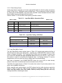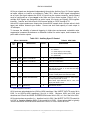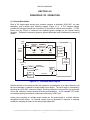
1
Rev: 082006
PMC66-16AI64SSA/C
64-CHANNEL 16-BIT SIMULTANEOUS SAMPLING
PMC ANALOG INPUT BOARD
With 200KSPS Sample Rate per Channel
and 66MHz PCI Support
and Triggered Bursts
_______________________
REFERENCE MANUAL
_____________________________________________________________________________
General Standards Corporation Ph:(256)880-8787 FAX:(256)880-8788 Email: [email protected]
MAN-PMC66-16AI64SSA/C
PMC66-16AI64SSA/C
Copyright (C) 2006 General Standards Corp.
Additional copies of this manual or other General Standards Co. literature may be obtained from:
General Standards Corp.
8302A Whitesburg Dr.
Huntsville, Alabama 35802
Telephone: (256) 880-8787
FAX:
(256) 880-8788
The information in this document is subject to change without notice.
General Standards Corp. makes no warranty of any kind with regard to this material, including, but not limited to, the implied
warranties of merchantability and fitness for a particular purpose. Although extensive editing and reviews are performed
before release to ECO control, General Standards Corp. assumes no responsibility for any errors that may exist in this
document. No commitment is made to update or keep current the information contained in this document.
General Standards Corp. does not assume any liability arising out of the application or use of any product or circuit described
herein, nor is any license conveyed under any patent rights or any rights of others.
General Standards Corp. assumes no responsibility resulting from omissions or errors in this manual, or from the use of
information contained herein.
General Standards Corp. reserves the right to make any changes, without notice, to this product to improve reliability,
performance, function, or design.
All rights reserved.
No part of this document may be copied or reproduced in any form or by any means without prior written consent of General
Standards Corp.
_____________________________________________________________________________
General Standards Corporation Ph:(256)880-8787 FAX:(256)880-8788 Email: [email protected]
PMC66-16AI64SSA/C
TABLE OF CONTENTS
SECTION
1.0
TITLE
______
INTRODUCTION
_
PAGE
1-1
1.1
General Description
1-1
1.2
Functional Overview
1-2
2.0
INSTALLATION AND MAINTENANCE
2-1
2.1
Board Configuration
2-1
2.2
Installation
2-1
2.2.1
Physical Installation
2-1
2.2.2
Input/Output Cable Connections
2-1
2.3
System Configuration
2-3
2.3.1
Analog Inputs
2-3
2.3.2
External Sync I/O
2-4
2.3.3
Multiboard Synchronization
2-5
2.4
Maintenance
2-5
2.5
Reference Verification
Equipment Required
2-5
2.5.1
2.5.2
3.0
Verification and Adjustment
CONTROL SOFTWARE
2-6
2-6
3-1
3.1
Introduction
3-1
3.2
Board Control Register (BCR)
3-1
3.3
Configuration and Initialization
3-2
3.3.1
Board Configuration
3-2
3.3.2
Initialization
3-3
3.4
Analog Input Parameters
3-3
3.4.1
Input Voltage Range
3-3
3.4.2
Timing Organization
3-3
3.4.3
Scan and Sync Control Register
3-4
3.4.4
Sample Rate Generators
3-4
3.4.4.1
Sample Rate Control
3-4
3.4.4.2
Generator Cascading
3-6
_____________________________________________________________________________
General Standards Corporation Ph:(256)880-8787 FAX:(256)880-8788 Email: [email protected]
i
PMC66-16AI64SSA/C
TABLE OF CONTENTS (Continued)
SECTION
3.4.5
3.5
3.5.1
TITLE
______
Multiboard Synchronization
Analog Input Control
Input Data Organization
_
PAGE
3-6
3-6
3-6
3.5.1.1
Input Data Buffer
3-6
3.5.1.2
Data Coding Format
3-7
3.5.2
Input Data Buffer Control
3-7
3.5.3
Analog Input Function Modes
3-8
3.5.3.1
3.5.3.2
System Analog Inputs
3-8
Selftest Modes
3-9
3.5.4
Sampling Modes
3-9
3.5.5
Differential Processing
3-9
3.5.5.1
Default Single-Ended Processing
3-9
3.5.5.2
Pseudo-Differential Mode
3-10
3.5.5.3
Full Differential Mode
3-10
3.5.5.4
Differential Scaling Considerations
3-10
3.6
Autocalibration
3-10
3.7
Interrupt Control
3-11
3.7.1
3.7.2
Local Interrupt Request
3-11
Enabling the PCI Interrupt
3-11
3.8
DMA Operation
3-12
3.9
Auxiliary External Sync I/O
3-13
3.10
Board Configuration Register
3-15
3.11
3.12
3.12.1
3.12.2
3.13
Data Packing
Triggered Bursts
Burst Size and Trigger Source
Sample Clock Source
Active Channel Group Assignment
3-15
3-16
3-16
3-16
3-17
4.0
PRINCIPLES OF OPERATION
4-1
4.1
General Description
4-1
4.2
Analog Inputs
4-2
4.3
Rate Generators
4-2
4.4
Data Buffer
4-2
4.5
Autocalibration
4-2
4.6
Power Control
4-2
App A
Local Control Register Quick Reference
A-1
App B
Migration from PMC-16AI64SS
B-1
_____________________________________________________________________________
General Standards Corporation Ph:(256)880-8787 FAX:(256)880-8788 Email: [email protected]
ii
PMC66-16AI64SSA/C
LIST OF ILLUSTRATIONS
FIGURE
TITLE
___
_
PAGE
1.1-1
Physical Configuration
1-1
1.2-1
Functional Organization
1-2
2.2-1
Input/Output Connector
2-3
2.3-1
Analog Input Configurations
2-4
2.3-2
Multiboard Synchronization
2-5
2.5-1
Reference Adjustment Access
2-6
3.4-1
Clock and Sync Organization
3-4
3.9-1
Auxiliary Sync Header
3-13
4.1-1
Functional Block Diagram
4-1
LIST OF TABLES
TABLE
TITLE
___ _
PAGE
2.2-1
System Connector Pin Functions
2-2
2.5-1
Reference Verification Equipment
2-6
3.1-1
Control and Data Registers
3-1
3.2-1
Board Control Register (BCR)
3-2
3.3-1
Configuration Operations
3-2
3.4-1
Analog Voltage Range Selection
3-3
3.4-2
Scan and Sync Control Register
3-5
3.4-3
Rate Generator Register
3-5
3.4-4
Rate Generator Frequency Selection
3-5
3.5-1
Input Data Buffer; Nonpacked Data
3-7
3.5-2
Input Data Coding; 16-Bit Data
3-7
3.5-3
Input Data Buffer Control Register
3-8
3.5-4
Buffer Size Register
3-8
3.5-5
Analog Input Function Selection
3-8
3.5-6
Differential Processing Modes
3-9
3.7-1
Interrupt Control Register
3-12
3.8-1
Typical DMA Registers; Block Mode
3-12
3.9-1
Auxiliary Sync I/O Connections
3-13
3.9-2
Auxiliary Sync I/O Control
3-14
3.10-1
Board Configuration Register
3-15
3.11-1
Data Packing
3-15
3.12-1
3.13-1
Burst Trigger Source
Active Channel Assignment
3-16
3-17
_____________________________________________________________________________
General Standards Corporation Ph:(256)880-8787 FAX:(256)880-8788 Email: [email protected]
iii
PMC66-16AI64SSA/C
SECTION 1.0
INTRODUCTION
1.1 General Description
The PMC66-16AI64SSA/C board is a single-width PCI mezzanine card (PMC) that provides
high-speed simultaneous 16-bit analog input capability for PMC applications. 64 analog input
lines can be digitized simultaneously at rates up to 200,000 conversions per second per
channel, with software-controlled voltage ranges of ±2.5V, ±5V, ±10V, 0 to +5V or 0 to +10V..
The board is functionally compatible with the IEEE PCI local bus specification Revision 2.3, and
is mechanically and electrically compatible with the IEEE compact mezzanine card (CMC)
specification IEEE 1386. A PCI interface adapter supports the "plug-n-play" initialization
concept.
Autocalibration determines offset and gain correction values for each input channel, and the
corrections are applied subsequently during acquisition. A selftest switching network routes
calibration reference signals to each channel through internal selftest switches, and permits
board integrity to be verified by the host.
Power requirements consist of +5 VDC from the PCI bus in compliance with the PCI
specification, and operation over the specified temperature range is achieved with conventional
air cooling. Specific details of physical characteristics and power requirements are contained in
the PMC66-16AI64SSA/C product specification. Figure 1.1-1 shows the physical configuration
of the board, and the arrangement of major components.
NOTE: Representative configuration. Details may vary.
SYSTEM I/O CONNECTOR
PMC HOST CONNECTORS
STANDOFF (4)
PRINTED CIRCUIT BOARD
5.87“ (149
MM)
P2
P1
PCI INTERFACE
ADAPTER
ANALOG COMPONENTS
SHIELD
POWER
CONTROL
SECTION
LOCAL
CONTROLLER
Figure 1.1-1. Physical Configuration
The board is designed for minimum off-line maintenance, and includes internal monitoring and
autocalibration features that eliminate the need for disconnecting or removing the module from
the system for calibration. All system input and output connections are made through a single
80-pin, dual-ribbon front-access I/O connector.
_____________________________________________________________________________
General Standards Corporation Ph:(256)880-8787 FAX:(256)880-8788 Email: [email protected]
1-1
PMC66-16AI64SSA/C
1.2 Functional Overview
Principal capabilities of the PMC66-16AI64SSA/C board are summarized in this list of features:
64 Single-Ended Simultaneously-Sampled 16-Bit Input Channels
Software-Selectable Analog Input Ranges of ±10V, ±5V, ±2.5V, 0/+5V or 0/+10V
512K-Sample Analog Input FIFO Buffer
Selectable Differential Processing
200 KSPS per Channel Conversion Rate (12.8 MSPS Aggregate Rate)
Dual Cascaded Internal Rate Generators
Supports Synchronization of Multiple Boards
Internal Autocalibration of all Analog Input Channels
Mastering DMA Engine
The 16-Bit PMC66-16AI64SSA/C analog input board samples and digitizes 64 input channels
simultaneously at rates up to 200,000 samples per second for each channel. The resulting
16-bit sampled data is available to the PCI bus through a 512K-Sample FIFO buffer. Each input
channel contains a dedicated 16-Bit sampling ADC. All operational parameters are software
configurable.
Input
Conn
Channel-00: One of 64 Identical Input Channels
Input
64 S.E.
Analog
Inputs
Vref
Selftest
Switching
Input
Attenuator
and Filter
16-Bit
ADC
Input Channels 01-63
Ext Sync
Local
Controller
Host Conn
(PCI)
+5VDC
Power
Conversion
PCI
Interface
Adapter
Regulated
Power Voltages
Data
Buffer
Vref
Local Bus
Figure 1.2-1. Functional Organization
Inputs can be sampled in groups of 2, 4, 8, 16, 32 or 64 channels, or any single channel can be
sampled continuously. The sample clock can be generated from an internal rate generator, or
directly through software, or by external hardware.
_____________________________________________________________________________
General Standards Corporation Ph:(256)880-8787 FAX:(256)880-8788 Email: [email protected]
1-2
PMC66-16AI64SSA/C
SECTION 2.0
INSTALLATION AND MAINTENANCE
2.1 Board Configuration
This product has no field-alterable configuration features, and is completely configured at
the factory for field use.
2.2 Installation
2.2.1 Physical Installation
To minimize the opportunity for accidental damage before installation, the board should be
stored in the original protective shipping envelope. System power must be turned OFF
before proceeding with the installation.
CAUTION:
This product is susceptible to damage from electrostatic discharge (ESD).
Before removing the board from the conductive shipping envelope, ensure
that the work surface, the installer and the host board have been properly
discharged to ground.
After removing the board from the shipping envelope, position the board with the shield and
standoffs facing the host (carrier) board, and with the I/O connector oriented toward the
front panel. Align the two PCI connectors located at the end of the board opposite the I/O
connector, with the mating connectors on the host board. Then carefully press the board
into position on the host. Verify that the PCI connectors have mated completely and that
the standoffs are seated against the host board.
Attach the board to the host with four 2.5 x 6.5mm panhead screws. Pass the screws
through the back of the host into the four mounting holes on the board. Tighten the screws
carefully to complete the installation. Do not overtighten.
2.2.2 Input/Output Cable Connections
System cable signal pin assignments are listed in Table 2.2-1. The I/O connector is
designed to mate with an 80-pin dual-ribbon connector, equivalent to Robinson Nugent
#P50E-080S-TG. The insulation displacement (IDC) Robinson Nugent cable connector
accepts two 40-wire 0.050-inch ribbon cables, with the pin numbering convention shown in
Table 2.2-1 and in Figure 2.2-1. Contact the factory if preassembled cables are required.
_____________________________________________________________________________
General Standards Corporation Ph:(256)880-8787 FAX:(256)880-8788 Email: [email protected]
2-1
PMC66-16AI64SSA/C
Table 2.2-1. System Connector Pin Functions
PIN
ROW-A SIGNAL
PIN
ROW-B SIGNAL
1
INP00
1
INP32
2
INP01
2
INP33
3
4
5
INP02
INP03
INPUT RTN
3
4
5
INP34
INP35
INPUT RTN
6
INP04
6
INP36
7
INP05
7
INP37
8
9
10
INP06
INP07
INPUT RTN
8
9
10
INP38
INP39
INPUT RTN
11
INP08
11
INP40
12
INP09
12
INP41
13
14
15
INP10
INP11
INPUT RTN
13
14
15
INP42
INP43
INPUT RTN
16
INP12
16
INP44
17
INP13
17
INP45
18
19
20
INP14
INP15
INPUT RTN
18
19
20
INP46
INP47
INP48
21
INP16
21
INPUT RTN
22
INP17
22
INP49
23
24
25
INP18
INP19
INPUT RTN
23
24
25
INP50
INP51
INP52
26
INP20
26
INP53
27
INP21
27
INPUT RTN
28
29
30
INP22
INP23
INPUT RTN
28
29
30
INP54
INP55
INP56
31
INP24
31
INP57
32
INP25
32
INP58
33
34
35
INP26
INP27
INPUT RTN
33
34
35
INPUT RTN
INP59
INP60
36
INP28
36
INP61
37
INP29
37
INP62
38
INP30
38
INP63
39
INP31
39
SYNC I/O RTN
40
INPUT RTN
40
SYNC I/O
_____________________________________________________________________________
General Standards Corporation Ph:(256)880-8787 FAX:(256)880-8788 Email: [email protected]
2-2
PMC66-16AI64SSA/C
ROW A
ROW B
PIN 40
I/O
CONN
PWB
PIN 1
Panel Pin-view
Figure 2.2-1. Input/Output Connector
2.3 System Configuration
2.3.1 Analog Inputs
Analog inputs INP00-INP63 (Table 2.2-1) can be configured as 1, 2, 4, 8, 16, 32 or 64
single-ended channels. Input configurations start at Channel-00, and proceed upward
through consecutive channels to the highest-numbered channel in the configuration. The
hardware input configuration must be acknowledged by the control software.
Single-ended inputs share a common input return that provides a return path for all inputs,
making isolation from other system grounds a critical issue. If the signal sources are
returned externally to system ground when operating in this mode, a potential difference
between the system ground and input return can cause erroneous measurements, or may
generate excessive ground current sufficient to damage the board.
A signal return pin (INPUT RTN) is provided in the I/O connector for every 4 or 5 input
channels. If the signal sources are isolated from each other, and from system ground
(Figure 2.3-1a), the returns in each 4 or 5 Channel group should be connected together at
the source, and to at least one INPUT RTN pin in the connector.
For signal sources that have a common isolated return at the source (Figure 2.3-1b), the
common return should be connected to at least one INPUT RTN pin for every 4 or 5 active
input channels.
To minimize crosstalk between input channels at higher frequencies, all INPUT RTN pins
should be connected to signal source returns. The INPUT-RTN pins are connected
together internally within the board, and are electrically common to the system or PCIbus
ground.
_____________________________________________________________________________
General Standards Corporation Ph:(256)880-8787 FAX:(256)880-8788 Email: [email protected]
2-3
PMC66-16AI64SSA/C
Analog Input Board
INPxx
4-5
Signal
Sources
INPxx
INPUT RTN
INPxx
4-5
Signal
Sources
INPxx
INPUT RTN
(Additional
signal
Groups)
INPxx
4-5
Signal
Sources
INPxx
INPUT RTN
INPxx
4-5
Signal
Sources
INPxx
INPUT RTN
(Additional
signal
Groups)
Figure 2.3-1. Analog Input Configurations
2.3.2 External Sync I/O
The SYNC I/O pin in the I/O connector is a bidirectional TTL synchronization signal that
provides external control of analog input sample triggering. The SYNC I/O signal is
referenced to the SYNC I/O RTN pin, which is connected internally to digital ground.
When configured as an input, this signal initiates a triggered sample of all active input
channels. The SYNC I/O input is asserted LOW, and is pulled HIGH internally through a
4.7 KOhm resistor. Minimum input pulse width is 140ns.
_____________________________________________________________________________
General Standards Corporation Ph:(256)880-8787 FAX:(256)880-8788 Email: [email protected]
2-4
PMC66-16AI64SSA/C
When configured as an output, the SYNC I/O signal is asserted for approximately 160
nanoseconds at the beginning of each scan. The SYNC I/O output signal is a TTL level that
can synchronize the operation of multiple target boards to a single initiator board. Like the
SYNC I/O input signal, the SYNC I/O output signal is asserted LOW. Loading of the SYNC
output should be limited to 10 milliamps or less.
Specific input/output configurations are determined by individual system requirements, and
must be acknowledged by the control software.
NOTE: Refer to Paragraph 3.9 for auxiliary external sync provisions.
2.3.3 Multiboard Synchronization
If multiple boards are to be synchronized together, the SYNC I/O and SYNC I/O RTN pins
from one board, the initiator, are connected to the SYNC I/O and SYNC I/O RTN pins of as
many as four target boards (Figure 2.3-2). The controlling software determines specific
synchronization functions.
Initiator Board
Or Other Sync Source
Target Board
#1
Target Board
#2
Sync
(Input)
Sync
(Input)
Sync
(Output)
Additional
Target Boards
Figure 2.3-2. Multiboard Synchronization
2.4 Maintenance
This product requires no scheduled hardware maintenance other than periodic reference
verification and possible adjustment. The optimum verification interval will vary, depending
upon the specific application, but in most instances an interval of one year is sufficient.
In the event of a suspected malfunction, all associated system parameters, such as power
voltages, control bus integrity, and system interface signal levels, should be evaluated
before troubleshooting of the board itself is attempted. A board that has been determined
to be defective should be returned to the factory for detailed problem analysis and repair.
2.5 Reference Verification
All analog input channels are software-calibrated to a single internal voltage reference by
an embedded autocalibration software utility. The procedure presented here describes the
verification and adjustment of the internal reference.
_____________________________________________________________________________
General Standards Corporation Ph:(256)880-8787 FAX:(256)880-8788 Email: [email protected]
2-5
PMC66-16AI64SSA/C
2.5.1 Equipment Required
Table 2.5-1 lists the equipment required for verifying or adjusting the internal reference.
Alternative equivalent equipment may be used.
Table 2.5-1. Reference Verification Equipment
EQUIPMENT DESCRIPTION
MANUFACTURER
MODEL
Digital Multimeter, 5-1/2 digit, 0.005%
accuracy for DC voltage measurements at
±10 Volts.
Hewlett Packard
34401A
Host board with single-width PMC adapter
(Existing host)
---
Test cable; suitable for connecting the
digital multimeter to two 0.024-inch square
test posts.
---
---
2.5.2 Verification and Adjustment
The following procedure describes the verification of the single reference voltage that
ensures conformance to the product specification. Adjustment of the internal reference, if
necessary, is performed with an internal trimmer that is accessible as shown in Figure
2.5-1.
This procedure assumes that the board is installed on an operational host board.
P2
P1
Shield
Internal Reference
Trimmer Access
Figure 2.5-1. Reference Adjustment Access
_____________________________________________________________________________
General Standards Corporation Ph:(256)880-8787 FAX:(256)880-8788 Email: [email protected]
2-6
PMC66-16AI64SSA/C
1.
Connect the digital multimeter between VCAL_PFS (+) Pin-3, and
REF RTN (-) Pin-4 in the J2 test connector.
2.
If power has been removed from the board, apply power now. Wait at least 10
minutes after power is applied before proceeding..
3.
Select the ±10V input range.
4.
Verify that the digital multimeter indication is +9.9900 VDC ±0.0009 VDC. If the
indication is not within this range, adjust the INTERNAL REFERENCE trimmer
until the digital multimeter indication is within the specified range.
5.
Verification and adjustment is completed. Remove all test connections.
_____________________________________________________________________________
General Standards Corporation Ph:(256)880-8787 FAX:(256)880-8788 Email: [email protected]
2-7
PMC66-16AI64SSA/C
SECTION 3.0
CONTROL SOFTWARE
3.1 Introduction
The PMC66-16AI64SSA/C board is compatible with the PCI Local Bus specification, and
supports auto-configuration at the time of power-up. A PLX™ PCI-9056 adapter operating in
J-mode controls the PCI interface, and supports both 33MHz and 66MHz PCI clock frequencies,
as well as D32 PCI bus width. Configuration-space registers are initialized internally to support
the location of the board on any 16-longword boundary in memory space. After initialization has
been completed, communication between the PCI bus and the local bus takes place through the
control and data registers shown in Table 3.1-1. All local data transfers are long-word D32.
Any of the predefined operational conditions identified throughout this section can invoke a
single interrupt request from the board. DMA access is supported for data transfers from the
analog input data buffer.
Table 3.1-1. Control and Data Registers
OFFSET
(Hex)
REGISTER
ACCESS
MODE*
DEFA ULT
PRIMARY FUNCTION
0000
BOARD CONTROL (BCR)
RW
0008 4060h
Board Control Register (BCR)
0004
INTERRUPT CONTROL
RW
0000 0008h
Interrupt conditions and flags
0008
INPUT DATA BUFFER
RO
000X XXXXh
Analog input data buffer
000C
INPUT BUFFER CONTROL
R/W
0003 FFFEh
Input buffer threshold and control
0010
RATE-A GENERATOR
RW
0001 0FA0h
Rate-A generator freq selection
0014
RATE-B GENERATOR
RW
0000 0050h
Rate-B generator freq selection
0018
BUFFER SIZE
RO
0000 0000h
Number of values in the input buffer
001C
BURST SIZE
R/W
0000 0001h
Number of sample clocks in a triggered burst.
0020
SCAN AND SYNC CONTROL
R/W
0000 0005h
Channels per scan; Clocking and Sync
sources.
0024
ACTIVE CHANNEL ASSIGNMENT
R/W
0000 0100h
Specific first and last active channels.
0028
Board Configuration **
RO
000X XXXXh
Firmware revision and option straps.
002C
Autocal Values **
R/W
0000 080Xh
Autocal value readback.
0030
Auxiliary R/W Register **
R/W
0000 0000h
Auxiliary register. For internal use only.
0034
Auxiliary Sync I/O Control
R/W
0000 0000h
Controls auxiliary sync I/O port
0038
Scan Marker Upper Word
R/W
0000 0000h
Packed-data scan marker D[31..16].
003C
Scan Marker Lower Word
R/W
0000 0000h
Packed-data scan marker D[15..0]..
R/W = Read/Write, RO = Read-Only.
** Maintenance register; shown for reference only.
3.2 Board Control Register (BCR)
The Board Control Register (BCR) controls primary board functions, including analog input
mode and range, and consists of 32 control bits and status flags. Table 3.2-1 provides a brief
description of each bit field in the BCR, as well as indicating an associated section in the text.
_____________________________________________________________________________
General Standards Corporation Ph:(256)880-8787 FAX:(256)880-8788 Email: [email protected]
3-1
PMC66-16AI64SSA/C
Table 3.2-1. Board Control Register (BCR)
Offset: 0000h
DATA BIT
MODE
D00-D02
R/W
D03
D04-D05
D06
Default: 0008 4060h
DEF
DESCRIPTION
REF
AIM[2..0]
0
Analog input mode. Selects system inputs or
selftest mode. Defaults to System Inputs
3.5.3
R/W
UNIPOLAR INPUTS
0
Selects unipolar inputs when HIGH, bipolar
inputs when LOW.
3.4.1
R/W
RANGE[1..0]
2
Analog input range. Defaults to ±10V range.
3.4.1
1
Selects offset-binary analog I/O data format
when asserted HIGH, or two's complement when
LOW.
3.5.1.2
3.9
R/W
DESIGNATION
OFFSET BINARY
D07
R/W
ENABLE EXTERNAL SYNC
0
Selects external sync I/O when HIGH.. (The
Scan and Sync control register selects TARGET
or INITIATOR mode).
Not required for bursting (3.12)
D08-D09
R/W
DIFFERENTIAL PROCESSING
0
Selects standard or differential processing.
D10-D11
R/W
(Reserved)
0
---
3.5.5
---
D12
R/W
*INPUT SYNC
0
Triggers a single sample of all active channels
when BCR Input Sync is selected in the Scan
and Sync Control Register.
D13
R/W
*AUTOCAL
0
Initiates an
asserted.
when
3.6
D14
RO
AUTOCAL PASS
1
Set HIGH at reset or autocal initialization.
A HIGH state after autocal confirms a successful
calibration.
3.6
D15
R/W
*INITIALIZE
0
Initializes the board when set HIGH.
register defaults.
D16
R/W
BUFFER UNDERFLOW
0
Set HIGH if the buffer is read while empty.
Cleared by direct write or by buffer clear.
3.5.2
D17
R/W
BUFFER OVERFLOW
0
Set HIGH if the buffer is written to when full.
Cleared by direct write or by buffer clear.
3.5.2
D18
R/W
ENABLE DATA PACKING
0
Enables local-bus data packing
3.11
D19
R/W
DISABLE DEMAND MODE
1
Disables demand mode DMA operation.
3.8
D20-D31
RO
(Reserved)
0
---
---
R/W = Read/Write, RO = Read-Only.
autocalibration
operation
Sets all
3.4.2
3.3.2
*Clears automatically when operation is completed
3.3 Configuration and Initialization
3.3.1 Board Configuration
During board configuration, initial values for both the PCI configuration registers and the internal
control logic are extracted from internal nonvolatile read-only memory. This process is initiated
by a PCI bus reset, and should be required only once after the initial application of power. While
the PCI configuration registers are being loaded, the response to PCI target accesses is
RETRY's. Configuration operations are executed in the sequence shown in Table 3.3-1.
Table 3.3-1. Configuration Operations
Operation
PCI configuration registers are loaded from internal ROM
Internal control logic is configured from internal ROM
Internal control logic is initialized
Maximum Duration
3 ms
300 ms
3 ms
_____________________________________________________________________________
General Standards Corporation Ph:(256)880-8787 FAX:(256)880-8788 Email: [email protected]
3-2
PMC66-16AI64SSA/C
Loading of the PCI configuration registers is completed within 3 milliseconds after the assertion
of a PCI bus reset, and should be required only once after the initial application of power. PCI
register configuration terminates with the PCI interrupt disabled.
3.3.2 Initialization
Internal control logic can be initialized without reconfiguration of the PCI registers by setting the
INITIALIZE control bit in the BCR. This action initializes the internal logic, but does not affect the
PCI configuration registers and does not reconfigure the internal control logic. Initialization
requires 3 milliseconds or less for completion, and produces the following default conditions:
• The BCR is initialized; all defaults are invoked,
• Analog input voltage range is ±10 Volts,
• 32 channels are active,
• Input sample clocking is from the Rate-A generator at 12,500 samples per second,
• Analog input data coding format is offset binary; Data packing is disabled,
• The analog input buffer is reset to empty,
• Input rate generator Rate-A is disabled (Rate Generator Register D16 = HI ).
Upon completion of initialization, the INITIALIZE control bit is cleared automatically.
3.4 Analog Input Parameters
3.4.1 Input Voltage Range
BCR control field RANGE[], as shown in Table 3.4-1 selects the analog input voltage range.
Table 3.4-1. Analog Voltage Range Selection
RANGE[1:0]
ANALOG INPUT RANGE
0
±2.5 Volts
1
±5 Volts
2
±10 Volts
3
±10 Volts
When the UNIPOLAR INPUTS control bit is HIGH in the BCR (Table 3.2-1), the ±2.5V and ±5V
input ranges become 0/+5V and 0/+10V, respectively.
3.4.2 Timing Organization
Figure 3.4-1 illustrates the manner in which timing signals are organized within the board. The
input sample clock selector is controlled by the Scan and Sync control register, which provides
direct software control of clocking and sync operations. The external sync input and output line
permits external control of timing. Two rate generators operate directly from the master clock
frequency, or can be cascaded.
A sample clock can be generated by either rate generator, by the INPUT SYNC control bit in the
BCR, or by an external sync source. Each Input Sample Clock triggers a sample of all active
input channels. An active channel group can contain from two to 64 channels, or any single
channel can be sampled individually. Each active channel group commences with Channel 00,
and proceeds upward through consecutive channels to the selected number of channels.
_____________________________________________________________________________
General Standards Corporation Ph:(256)880-8787 FAX:(256)880-8788 Email: [email protected]
3-3
PMC66-16AI64SSA/C
Selector
BCR Input-Sync Bit
Gen
A
Master Clock
Nrate
A
Fgen-A
Sample Clock
Gen Fgen-B
B
Nrate
B
(Initiator)
Ext Sync Input/Output
(Target)
Figure 3.4-1. Clock and Sync Organization
3.4.3 Scan and Sync Control Register
The Scan and Sync control register (Table 3.4-2) controls the configuration of internal timing
signals. The ACTIVE CHANNELS control field selects the number of active channels from two
channels to 64 channels, or selects the single-channel mode if zero. (See Paragraph 3.5.5;
Sampling Modes).
3.4.4 Sample Rate Generators
Each of the two rate generators consists of a 16-bit down-counter that divides the master clock
frequency by a 16-bit integer contained in the associated rate register. The two rate registers
are organized as shown in Table 3.4-3. Bits D00-D15 represent the frequency divisor Nrate,
and D16 disables the associated generator when set HIGH. To prevent the input buffer from
filling with extraneous data at power-up, D16 defaults to the HIGH state in the Rate-A control
register.
3.4.4.1 Sample Rate Control
Each rate generator is controlled by a divisor Nrate that can be adjusted up to a maximum value
of FFFFh (65535 decimal). With a master clock frequency of Fclk (MHz), the output frequency
Fgen of each generator is determined as:
Fgen (Hz) = Fclk (Hz) / Nrate,
where Nrate is the decimal equivalent of D00-D15 in the rate generator register. Fgen is the
sampling frequency, and equals the rate at which all active channels are sampled. Fclk has a
standard value of 50.000MHz, but may have other values depending upon custom ordering
options.
The maximum sampling frequency Fgen-max is 200 kHz.
_____________________________________________________________________________
General Standards Corporation Ph:(256)880-8787 FAX:(256)880-8788 Email: [email protected]
3-4
PMC66-16AI64SSA/C
Table 3.4-2. Scan and Sync Control Register
Offset: 0020h
DATA
BIT
MODE
D00-D02
R/W
Default: 0000 0005h
DESIGNATION
DEF
ACTIVE CHANNELS
5
DESCRIPTION
Number of active input channels:
0
1
2
3
4
5
6
7
=> Single-Channel mode *
=> 2 channels (00-01)
=> 4 channels (00-03)
=> 8 channels (00-07)
=> 16 channels (00-15)
=> 32 channels (00-31); Default value
=> 64 channels (00-63)
=> Channel group assignment (See Section 3.13)
* Channel selected by Single-Channel Select field below.
D03-D04
R/W
SAMPLE CLOCK SOURCE
0
Selects the analog input sample clocking source:
0 => Internal Rate-A generator output
1 => Internal Rate-B generator output
2 => External Sync input line (Selects TARGET mode)
3 => BCR Input Sync control bit.
(See also Triggered Burst, Section 3.12).
D05-D06
R/W
(Reserved)
0
---
D07
RO
BURST BUSY
0
Indicates a burst in progress.
D08-D09
R/W
BURST ON SYNC
0
Selects the triggered burst acquisition mode (Section 3.12)
D10
R/W
RATE-B CLOCK SOURCE
0
Selects the clock input source for the Rate-B generator:
0 => Master clock
1 => Rate-A generator output.
D11
R/W
(Reserved)
0
---
D12-17
R/W
SINGLE-CHANNEL SELECT
0
Selects the input channel number when operating in the
Single-Channel scanning mode.
D18
R/W
(Reserved)
0
---
D19-D31
RO
(Reserved)
0
Inactive
R/W = Read/Write, RO = Read-Only.
Table 3.4-3. Rate Generator Register
Offset: 0010h (Rate-A), 0014h (Rate-B)
DESIGNATION
Default: 0001 0FA0 (Rate-A), 0000 0050h (Rate-B)
DATA BIT
MODE*
D00-D15
R/W
D16
R/W
GENERATOR DISABLE
1
Disables the rate generator when HIGH
D17-D31
RO
(Inactive)
0
---
NRATE
DEFAULT
---
DESCRIPTION
Rate generator frequency control
R/W = Read/Write, RO = Read-Only.
Table 3.4-4. Rate Generator Frequency Selection
Nrate
(Dec)
( RATE[15..0] )
(Hex)
250
00FA
251
00FB
---
---
FREQUENCY Fgen (30 MHz Master Clock)*
(Hz)
200,000
199,203
Fgen (Hz) = 50,000,000 / Nrate
* ±0.015 percent.
_____________________________________________________________________________
General Standards Corporation Ph:(256)880-8787 FAX:(256)880-8788 Email: [email protected]
3-5
PMC66-16AI64SSA/C
3.4.4.2 Generator Cascading
To provide very low sample rates, the Rate-B generator can be configured with the RATE-B
CLOCK SOURCE control field to operate from the output of the Rate-A generator instead of
from the master clock. When operating in this cascaded configuration, the output frequency of
the Rate-B generator is:
Fgen-B (Hz) = Fclk / (Nrate-A * Nrate-B ) ,
which can produce sample rates as low as 0.012 Hz with Fclk = 50 MHz.
3.4.5 Multiboard Synchronization
Multiple boards can be interconnected externally to produce synchronous analog input
sampling. Figure 2.3-2 illustrates the interconnections required. External sync I/O is enabled
by setting the ENABLE EXTERNAL SYNC control bit HIGH in the BCR. One of the boards is
designated as the Initiator, and the remaining boards are designated as targets.
A board that is enabled for external sync I/O is designated as a target by selecting External
Sync Input Line in the SAMPLE CLOCK SOURCE control field in the Scan and Sync control
register. Any other value for this field designates the board as an initiator. The sync signal can
originate either from an initiator board, or externally as an input to a group of targets.
If the ENABLE EXTERNAL SYNC control bit is set HIGH in the BCR, an initiator generates a
sync pulse at the selected sample rate, and each of the target boards responds to the sync
pulse by acquiring a single sample of all of its designated active channels.
NOTES: To avoid contention on the SYNC I/O line, all initiator/target designations
should be assigned before enabling external sync I/O operation. No more
than one board can be designated as an initiator.
For optimum autocalibration effectiveness at rates above 20KSPS, adjust
the Rate-A Generator register to the same value on all boards.
Refer to Paragraph 3.9 for alternative external sync provisions.
3.5 Analog Input Control
3.5.1 Input Data Organization
Processed conversion data from the analog-to-digital converters (ADC's) flows directly into the
512K-sample analog input FIFO data buffer, and from the data buffer to the PCI bus as analog
input data. The data buffer appears to the PCI bus as a single read-only register.
3.5.1.1 Input Data Buffer
Nonpacked analog input data is right-justified to the LSB, and occupies bit positions D00
through D15 (Table 3.5-1). D16 is HIGH for all Channel 00 values, and LOW for data from all
other channels. Bits D17-D31 are always returned as zeros. An empty buffer returns an
indeterminate value. Refer to Paragraph 3-11 for the configuration of packed data.
_____________________________________________________________________________
General Standards Corporation Ph:(256)880-8787 FAX:(256)880-8788 Email: [email protected]
3-6
PMC66-16AI64SSA/C
3.5.1.2 Data Coding Format
Analog input data is arranged as 16 active right-justified data bits with the coding conventions
shown in Table 3.5-2. The default format is offset binary. Two's complement format is selected
by clearing the OFFSET BINARY control bit LOW in the BCR. Unless indicated otherwise, offset
binary coding is assumed throughout this document.
Refer to Section 3.11 for the effect of data packing on buffer contents.
Table 3.5-1. Input Data Buffer; Nonpacked Data
Offset: 0008h
Default: N/A
DATA BIT
MODE*
DESIGNATION
DESCRIPTION
D00
RO
DATA00
Least significant data bit
D01-D14
RO
DATA01 - DATA14
Intermediate data bits
D15
RO
DATA15
Most significant data bit
D16
RO
CHANNEL 00 TAG
Indicates a Channel-00 data value
D17-D31
RO
(Inactive)
---
* RO indicates read-only access. Write-data is ignored.
Table 3.5-2. Input Data Coding; 16-Bit Data
ANALOG INPUT LEVEL
DIGITAL
OFFSET BINARY
VALUE (Hex)
TWO'S COMPLEMENT
Positive Full Scale minus 1 LSB
0000 FFFF
0000 7FFF
Zero
0000 8000
0000 0000
Zero minus 1 LSB
0000 7FFF
0000 FFFF
Negative Full Scale
0000 0000
0000 8000
3.5.2 Input Data Buffer Control
The Input Data Buffer control register shown in Table 3.5-3 controls and monitors the flow of
data through the analog input data buffer. Asserting the CLEAR BUFFER control bit HIGH
clears, or empties, the buffer. The Threshold Flag is HIGH when the number of values in the
input data buffer exceeds the input threshold value defined by bits D00-D17, and is LOW if
the number is equal to or less than the threshold value. An interrupt (Section 3.7) can be
programmed to occur on either the rising or falling edge of the threshold flag.
Input data is discarded if the DISABLE BUFFER control bit is set HIGH, but data already
present in the buffer is unaffected and can be accessed from the PCIbus.
The Buffer Size register shown in Table 3.5-4 contains the number of input values present in the
buffer, and is updated continuously.
Buffer underflow and overflow flags in the BCR indicate that the buffer has been read while
empty or written to when full. Each of these situations is indicative of data loss. Once set
HIGH, each flag remains HIGH until cleared, either by directly clearing the bit LOW or by
clearing the buffer or initializing the board.
_____________________________________________________________________________
General Standards Corporation Ph:(256)880-8787 FAX:(256)880-8788 Email: [email protected]
3-7
PMC66-16AI64SSA/C
Table 3.5-3. Input Data Buffer Control Register
Offset: 000Ch
Default: 0003 FFFEh
DATA BIT
MODE*
DESIGNATION
DEF
D00-D17
R/W
THRESHOLD VALUE
D18
R/W
CLEAR BUFFER *
0
Clears (empties) the input buffer and processing
pipeline when asserted HIGH.
D19
RO
THRESHOLD FLAG
0
Asserted HIGH when the number of values in the
input buffer exceeds the THRESHOLD VALUE.
D19-D31
RO
(Inactive)
0
---
FFFEh
DESCRIPTION
Input buffer threshold value.
*Clears automatically within 200ns of being set
Table 3.5-4. Buffer Size Register
Offset: 0018h
Default: 0000 0000h
DATA BIT
MODE*
DESIGNATION
D00-D17
RO
BUFFER SIZE
D18-D31
RO
(Inactive)
DEF
00000h
0
DESCRIPTION
Number of values in the input buffer
---
3.5.3 Analog Input Function Modes
BCR control field AIM[] selects the analog input signal source, and provides selftest modes for
monitoring the integrity of the analog input networks. Table 3.5-5 summarizes the input function
modes.
3.5.3.1 System Analog Inputs
With the default value of 'Zero' selected for the AIM[] field in the BCR, all ADC channels are
connected to the system analog inputs from the system I/O connector.
Table 3.5-5. Analog Input Function Selection
AIM[2:0]
FUNCTION OR MODE
0
System analog input mode (Default mode).
1
(Reserved)
2
ZERO test. Internal ground reference is connected to all analog input channels.
3
+VREF test. Internal voltage reference is connected to all analog input channels.
4-7
(Reserved)
_____________________________________________________________________________
General Standards Corporation Ph:(256)880-8787 FAX:(256)880-8788 Email: [email protected]
3-8
PMC66-16AI64SSA/C
3.5.3.2 Selftest Modes
In the selftest modes, the analog input lines from the system I/O connector are ignored and
have no effect on selftest results.
Specified board accuracy applies to all selftest
measurements, and the averaged values of multiple samples should be used for critical
measurements.
The ZERO selftest applies a Zero reference signal to all input channels, and should produce a
nominal midscale reading of 0000 8000h for bipolar inputs, or 0000 0000h for unipolar inputs.
For the +VREF test, a precision reference voltage is applied to all inputs. The +VREF
reference voltage equals 99.90% of the positive fullscale value (nominally 0000 FFDFh)
for bipolar ranges, or 49.95% (nominally 0000 7FDF)for unipolar ranges.
3.5.4 Sampling Modes
The analog inputs can be sampled in groups of 2, 4, 8, 16, 32 or 64 active channels, or any
single channel can be selected for digitizing. The number of active channels is selected by the
ACTIVE CHANNELS[] field in the scan and sync control register. Each active channel group
commences with Channel-00, and proceeds upward through successive channels to the
selected number of channels.
For Single-Channel sampling (ACTIVE CHANNELS[] = 0), the channel to be digitized is
selected by the SINGLE-CHANNEL SELECT control field.
NOTE: Refer to Section 3.13 to designate a specific group of active channels.
3.5.5 Differential Processing
Although the hardware inputs are single-ended in nature, differential processing allows the
inputs to appear as either pseudo-differential or full-differential channels. Each of these
processing modes is characterized by the reference from which the signal in each channel is
measured. Differential processing is selected by the DIFFERENTIAL PROCESSING control
field in the BCR as shown in Table 3.5-6.
Table 3.5-6. Differential Processing Modes
BCR
D08,09
Designation
Processing Function
0
SINGLE ENDED
Default operating mode. Processing of input data is limited to
gain and offset error correction.
1
PSEUDO-DIFFERENTIAL
Channel-00 is the input LO reference for all other channels.
2
FULL DIFFERENTIAL
Each odd-numbered channel is the LO reference for each
even-numbered HI channel. I.e.: Channels 00 and 01 become
Channel-00 HI and Channel-00 LO, respectively.
3
(Reserved)
3.5.5.1 Default Single-Ended Processing
For single-ended channels, each input signal is measured with respect to the common input
return. That is, each channel reports the difference between the input signal voltage and the
voltage present on the common input return. This configuration provides the maximum number
of input channels, but allows noise and other forms of interference on the common return line to
appear in the signal measurement.
_____________________________________________________________________________
General Standards Corporation Ph:(256)880-8787 FAX:(256)880-8788 Email: [email protected]
3-9
PMC66-16AI64SSA/C
3.5.5.2 Pseudo-Differential Mode
Pseudo-differential processing designates input Channel-00 as the reference for all other
channels, and subtracts the sampled value in Channel-00 from the sampled values in all other
channels. With this arrangement, noise and interference on the common return line is
essentially cancelled, and the Channel-00 input line can be used as a 'remote sense' line for
Channels 01-63. Channel-00 can no longer be used as a measurement channel when
operating in this mode, and appears in the acquisition sequence with a zero-level value.
3.5.5.3 Full Differential Mode
If full-differential processing is selected, each odd-numbered channel becomes the reference
level for the associated even-numbered channel. For example, Channel-01 becomes the
reference for Channel-00, and Channel-00 data is reported as the difference between the actual
Channel-00 input signal and the signal in Channel-01. Odd-numbered channels do not
appear in the data buffer when operating in full-differential mode, which reduces the
number of data channels to one-half the number of active channels selected in the Scan
and Sync control register (Table 3.4-2).
Note: Because the same signal is applied to all channels simultaneously when a selftest
operation is selected (3.5.3.2), selftest always produces a zero-level when
operating in either differential processing mode.
3.5.5.4 Differential Scaling Considerations
Because differential processing operates by subtracting the signal values in two channels, all
input ranges are effectively doubled when either differential mode is selected. With the ±10V
range and pseudo-differential operation selected for example, Channel-00 data can have any
value from -10V to +10V, and all channels using Channel-00 as a reference also have the same
range of values. The difference signal then can have any value from -20V to +20V, and the
effective input range becomes ±20V.
Note: Although differential processing effectively doubles the output data range, the
hardware input levels are still restricted to the selected input range.
In addition to doubling the effective input voltage range, differential processing also always
produces a bipolar output signal. Since a reference channel can have a value that is greater
than or less than that in a signal channel, differentially processed data is always bipolar in
nature.
3.6 Autocalibration
To obtain maximum measurement accuracy, autocalibration should be performed after:
• Power warmup or a PCIbus reset,
• Input range change,
• Sample rate change, if greater than 20 kHz.
A small error, on the order of 0.04-percent, can be introduced when the input range is changed,
or when a large change (>20 kHz) occurs in the sample rate. Performing autocalibration with
the required sample rate selected eliminates this error.
_____________________________________________________________________________
General Standards Corporation Ph:(256)880-8787 FAX:(256)880-8788 Email: [email protected]
3-10
PMC66-16AI64SSA/C
During autocalibration, no control settings are altered and external analog input signals are
ignored.
Autocalibration is invoked by setting the AUTOCAL control bit HIGH in the BCR. The control bit
returns LOW automatically at the end of autocalibration. Autocalibration can be invoked at any
time, and has a duration of approximately 0.5 second. Completion of the operation can be
detected either by selecting the 'Autocalibration Operation Completed' interrupt condition
(paragraph 3.7) and waiting for the interrupt request, or by simply waiting a sufficient amount of
time to ensure that autocalibration has been completed.
To compensate for component aging, and to minimize the effects of temperature on accuracy,
the autocalibration function determines the optimum calibration values for current conditions,
and stores the necessary correction values in volatile memory. If a board is defective, the
autocalibration process may be unable to successfully calibrate the inputs. If this situation
occurs, the AUTOCAL PASS status bit in the BCR is cleared LOW at the end of the
autocalibration interval, and remains LOW until a subsequent initialization or autocalibration
occurs. AUTOCAL PASS is initialized HIGH, and remains HIGH unless an autocalibration
failure occurs.
NOTE: For synchronous multiple-board operation at rates above 20KSPS, adjust the
Rate-A Generator register to the same value on all boards (3.4.4.2).
3.7 Interrupt Control
In order for the board to generate a PCI interrupt, both of the following conditions must occur:
a. The internal controller must generate a Local Interrupt Request (Section 3.7.1)
b. The PCI interrupt must be enabled (Section3.7.2).
If the internal controller generates a local interrupt request, a PCI bus interrupt will not occur
unless the PCI interrupt has been enabled as described in Paragraph 3.7.2.
3.7.1 Local Interrupt Request
The Interrupt Control Register shown in Table 3.7-1 controls the single local interrupt request
line. Two simultaneous source conditions (IRQ 0 and1) are available for the request, with
multiple conditions available for each source.
IRQ 0 and 1 are logically OR'd together to
produce the single interrupt available to the board.
When one or more selected conditions occur for either of the IRQ's, a local interrupt request is
generated and the associated IRQ REQUEST flag bit is set HIGH. The request remains
asserted until the PCI bus clears the request flag. A local interrupt request is generated
automatically at the end of initialization, through IRQ0.
Interrupt conditions are edge-sensitive, and an interrupt request is generated if, and only if, a
specific interrupt condition undergoes a transition from 'false' (not-true) to 'true' while that
condition is selected.
3.7.2 Enabling the PCI Interrupt
A local interrupt request will not produce an interrupt on the PCI bus unless the PCI interrupt is
enabled. The PCI interrupt is enabled by setting the PCI Interrupt Enable and Local Interrupt
Input Enable control bits HIGH in the Runtime Interrupt Control/Status Register described in
Section 6 of the PLXTM PCI-9056 reference manual..
_____________________________________________________________________________
General Standards Corporation Ph:(256)880-8787 FAX:(256)880-8788 Email: [email protected]
3-11
PMC66-16AI64SSA/C
Table 3.7-1. Interrupt Control Register
Offset: 0000 0004h
DATA BIT
MODE
D00-02
R/W
Default: 0000 0008h
DESIGNATION
IRQ0 A0,1,2
DEF
VALUE
0
0
INTERRUPT EVENT
Idle. Interrupt disabled unless initializing.
Default state after reset.
1
Autocalibration operation completed
2
Input sample initiated (Sync)
3
Input sample completed (data ready)
4
Triggered burst initiated (BURST BUSY => HI)
5
Triggered burst completed (BURST BUSY => LO)
6-7
(Reserved)
D03
R/W
IRQ0 REQUEST
1*
---
Group 0 interrupt request flag. Set HIGH when the
selected interrupt condition occurs. Clears the request
when cleared LOW by the bus.
D04-06
R/W
IRQ1 A0,1
0
0
Idle; no interrupt condition selected.
1
Input buffer threshold LOW-HIGH transition
2
Input buffer threshold HIGH-LOW transition
3-7
(Reserved)
Group 1 interrupt request flag. See D03.
D07
R/W
IRQ1 REQUEST
0
---
D08-31
RO
(Inactive)
0
---
R/W = Read/Write, RO = Read-Only.
* HIGH after reset.
3.8 DMA Operation
DMA transfers from the analog input buffer are supported with the board operating as bus
master in DMA Channel 0 or 1. Table 3.8-1 illustrates a typical PCI register configuration that
controls a non-chaining, non-incrementing 'block-mode' DMA transfer in DMA Channel-0, and
in which a PCI interrupt is generated when the transfer has been completed.
Bit 02
(0000 0004h) in the PCI Command register must be set HIGH to select the bus mastering
mode. Refer to a PCI-9056 reference manual for a detailed description of these registers.
For most applications, the DMA Command Status register would be initialized to the value
0000 0001h, and then changed to 0000 0003h to initiate a transfer.
Table 3.8-1. Typical DMA Registers; Block-Mode
PCI Offset
PCI Register
Function
Typical Value
80h
DMA Mode
Bus width (32); Interrupt on done
0002 0D43h
84h
DMA PCI Address
Initial PCI data source address
88h
DMA Local Address
Analog Input Buffer local address
(Analog input buffer)
8Ch
DMA Transfer Byte Count
Number of bytes in transfer
90h
DMA Descriptor Counter
Transfer direction; Local bus to PCI bus
(Analog inputs)
0000 000Ah
A8h
DMA Command Status
Command and Status Register
0000 0001h
0000 0003h
(See Text)
*
0000 0008h
*
* Determined by specific transfer requirements.
_____________________________________________________________________________
General Standards Corporation Ph:(256)880-8787 FAX:(256)880-8788 Email: [email protected]
3-12
PMC66-16AI64SSA/C
Bits12 and 15 in the PCI-9056 DMA Mode register, when HIGH, select 'demand-mode' DMA
operation in slow-terminate mode, in which a DMA transfer is requested automatically when the
number of values in the buffer exceeds the threshold value selected for the buffer.
The DMA request is sustained until one of the following events occurs:
(a)
(b)
(c)
(d)
(e)
The data buffer goes empty,
The number of values read from the buffer equals the threshold value plus one,
The buffer is cleared,
The board is reset,
Autocalibration is executed.
The DMA request is terminated at the first occurrence of any of these events.
Note: The DISABLE DEMAND MODE control bit in the BCR must be cleared LOW in order
for the local controller to acknowledge demand mode operation.
Note:
To avoid encountering Lword alignment issues, demand mode DMA transfers
should be quad-word aligned (X0h/X8h).
3.9 Auxiliary External Sync I/O
Four auxiliary external connections provide an alternate method of synchronizing sample
clocking to external events when the ENABLE EXTERNAL SYNC control bit is HIGH in the
BCR. These TTL connections are available as AUX-0 through AUX-3 (Table 3.9-1), and are
accessible both through a 6-Pin header on one edge of the board, and through the two PMC
PCI-interface connectors P1 and P2.
Table 3.9-1. Auxiliary Sync I/O Connections
SIGNAL
PIN *
PMC CONN PIN
AUX-0
1
P1-41
AUX-1
2
P1-42
AUX-2
3
P2-10
AUX-3
4
P2-34
Pin-View
RETURN
5,6
(PCI GND)
Figure 3.9-1. Auxiliary Sync Header
1
2
Pin 5
6
PWB
* 2-Row 2mm right-angle header.
_____________________________________________________________________________
General Standards Corporation Ph:(256)880-8787 FAX:(256)880-8788 Email: [email protected]
3-13
PMC66-16AI64SSA/C
AUX sync signals are designated independently through the Auxiliary Sync I/O Control register
as inputs, outputs, or inactive, as indicated in Table 3.9-2. When an AUX signal is designated
as an input, the signal replaces the SYNC IO input from the system connector, and the board
must be configured as a sync target in the Scan and Sync control register (Table 3.4-2). If
multiple AUX signals are designated as active inputs, the inputs are logically OR'd together
internally. 'Inactive' and 'Active Input' AUX lines are pulled to +5VDC through 4.7K.
Active AUX outputs produce an output pulse for each ADC sample clock, and are active in both
target and initiator external sync modes. Source and sink load capacity of each output is
15 milliamps.
To increase the reliability of external triggering in high-noise environments, selectable noise
suppression increases the debounce or detection interval for active inputs, and increases the
pulse width of active outputs.
Table 3.9-2. Auxiliary Sync I/O Control
Offset: 0000 0034h
Default: 0000 0000h
DATA
BIT
MODE
D00-01
R/W
AUX-0 Control Mode
0
AUX-0 I/O Control Mode:
0 => Inactive
1 => Active Input (LO-to-HI edge)
2 => Active Output (Positive pulse)
3 => (Reserved)
D02-03
R/W
AUX-1 Control Mode
0
AUX-1 I/O Control Mode *
D04-05
R/W
AUX-2 Control Mode
0
AUX-2 I/O Control Mode *
D06-07
R/W
AUX-3 Control Mode
0
AUX-3 I/O Control Mode *
D08
R/W
INVERT INPUTS
0
Active inputs are detected on the LO-to-HI edge
when this bit is LOW, or on the HI-to-LO edge
when this bit is HIGH.
D09
R/W
INVERT OUTPUTS
0
Active outputs produce HIGH pulses when this bit
is LOW, or LOW pulses when this bit is HIGH.
D10
R/W
NOISE SUPPRESSION
0
When LOW, input debounce time is 100ns-135ns
and output pulse width is 135ns.
When HIGH, input debounce time is 1.5us, and
output pulse width is 2.0us.
D11-31
RO
(Reserved)
0
Read-back as all-zero.
DESIGNATION
DEFAULT
DESCRIPTION
* Same configuration as AUX-0.
AUX inputs are edge-detected as LOW-to-HIGH transitions if the INVERT INPUTS control bit is
LOW, or as HIGH-to-LOW transitions if the bit is HIGH. Minimum HIGH and LOW level
durations are 135ns if the NOISE SUPPRESSION control bit is LOW, or 1.5us if the bit is HIGH.
AUX output pulses are positive (i.e.: baseline level is LOW) if the INVERT OUTPUTS control bit
is LOW, or negative (baseline HIGH) if the control bit is HIGH. Output pulse width is typically
135ns if the NOISE SUPPRESSION control bit is LOW, or 2.0us if the bit is HIGH.
_____________________________________________________________________________
General Standards Corporation Ph:(256)880-8787 FAX:(256)880-8788 Email: [email protected]
3-14
PMC66-16AI64SSA/C
3.10 Board Configuration Register
The read-only board configuration register (Table 3.10-1) contains the existing firmware
revision, and a status field that indicates the configuration of optional features.
Table 3.10-1. Board Configuration Register
Offset: 0000 0028h
Default: 000X XXXXh
BIT FIELD
D00-D11
D12-D15
D16
D17-D18
DESCRIPTION
Firmware Revision
(Reserved status flags).
High if the board contains only 32 input channels.
Describes Master Clock Frequency Fclk as:
0 => 50.000 MHz
1 => 45.000 MHz
2 => 49.152 MHz
3 => 51.840 MHz
(Reserved)
D19-D31
3.11 Data Packing
Setting the ENABLE DATA PACKING control bit high in the BCR selects the data packing
mode, in which two consecutive 16-bit data values are packed into a single 32-Bit local data
longword. In the data packing mode, a 32-bit scan marker code is inserted directly before each
Channel-00 data value in the buffer.
The scan marker code is defined by the 'Scan Marker Upper Word' and 'Scan Marker Lower
Word' registers listed in Table 3.1-1, and is inserted immediately before the first (Channel-00)
value in each data scan as shown in Table 3.11-1. The lower 16 bits in each register contains
one word of the code. The upper 16 bits of these registers are ignored, and should be written
as all-zero.
Table 3.11-1. Data Packing
Buffer Data Field
ENABLE DATA PACKING = 0
Buffer Lword
Order
D[31..16]
ENABLE DATA PACKING = 1
D[15..0]
D[31..16]
D[15..0]
00
0001h
Chan 00 Data
Upper Marker
Lower Marker
01
0000h
Chan 01 Data
Chan 01 Data
Chan 00 Data
02
0000h
Chan 02 Data
Chan 03 Data
Chan 02 Data
03
0000h
Chan 03 Data
Chan 05 Data
Chan 04 Data
---
---
---
---
---
Some applications may require the scan marker code to be absolutely unique and not appear
randomly in the data. To support this requirement, an all-zero marker code (0000 0000h)
causes every all-zero data value (0000h) to be forced to a unit code (0001h) when data packing
is enabled. This arrangement supports the uniqueness requirement without affecting the
differential nonlinearity of the data itself.
_____________________________________________________________________________
General Standards Corporation Ph:(256)880-8787 FAX:(256)880-8788 Email: [email protected]
3-15
PMC66-16AI64SSA/C
3.12 Triggered Bursts
When the BURST ON SYNC control field is nonzero in the Scan and Sync control register
(Table 3.4-2), the context of a sync event changes from "sample on sync" to "burst on sync."
In the "sample on sync" context, a sync event initiates a single sample of all active channels
(See Sections 3.4.2 and 3.4.5). In the "burst on sync" context, a sync event initiates a burst of
internal sample clocks, each of which produces a sample of all active channels. This function is
available in firmware revisions 0200h through 04FFh (3.10).
3.12.1 Burst Size and Trigger Source
The number of sample clocks issued during a burst is controlled by the 20-bit Burst Size
control register listed in Table 3.1-1, which has a range from 1 to 1,048,575 sample clocks.
For Burst-Size values of one or greater, the number of sample clocks in a burst equals the value
in the register. For example, if a burst size of 10 is selected while 16 channels are active, then
each burst will contain 160 sample values. Selection of the burst trigger source is summarized
in Table 3.12-1. A Burst-Size of zero produces a burst that extends continuously until stopped,
either by disabling the internal clock or by clearing the BURST ON SYNC control field.
Table 3.12-1. Burst Trigger Source
Scan and Sync Register
BURST ON SYNC
Burst Trigger Source
Sync I/O Pin
0
Bursting disabled.
(Sample-Clock I/O)
1
Rate-B generator.
Trigger Output *
2
External Sync I/O input pin (or AUX input)
Trigger Input *
3
INPUT SYNC control bit in the BCR.
Trigger Output *
* Independent of BCR control bit ENABLE EXTERNAL SYNC.
The Sync I/O pin in the system I/O connector can operate as an input or output trigger pin. The
trigger output can serve as a burst trigger for target boards in which the BURST ON SYNC
control field selects the external Sync I/O pin as a trigger source. The burst trigger selection
supersedes the sample clock selection for control of the external Sync-I/O pin.
NOTE: During a triggered burst the BURST BUSY status flag in the Scan and Sync control
register goes HIGH at the trigger event, and returns LOW at the end of the burst. Either
edge of the BURST BUSY flag is selectable as an interrupt event (Table 3.7-1).
3.12.2 Sample Clock Source
When operating in the triggered-burst mode, the sample-clock source is selected by the
SAMPLE CLOCK SOURCE field in the Scan and Sync control register. The single restriction on
the sample clock source is that the burst trigger and the sample clock can not use the same
source simultaneously.
The following sequence illustrates the setup for a typical burst operation:
1. Select the input range, sample-clock source and burst size, with clocking disabled,
2. Select the burst trigger source (enables burst triggering),
3. Clear the buffer, then enable clocking.
_____________________________________________________________________________
General Standards Corporation Ph:(256)880-8787 FAX:(256)880-8788 Email: [email protected]
3-16
PMC66-16AI64SSA/C
3.13 Active Channel Group Assignment
If "Channel group assignment" is selected in the ACTIVE CHANNELS field in the Scan and
Sync control register (Table 3.4-2), the first and last active channels are defined by the Active
Channels Assignment control register shown in Table 3.13-1. The group of active channels is
contiguous, beginning with the channel designated by the FIRST CHANNEL SELECT field, and
proceeding upward through consecutive channels to (and including) the channel designated by
LAST CHANNEL SELECT. The LAST CHANNEL SELECT field must be greater than the
FIRST CHANNEL SELECT field.
Table 3.13-1. Active Channel Assignment
Offset: 0000 0024h
Default: 0000 0100h
DATA BIT
MODE
D00-D07
R/W
FIRST CHANNEL SELECT
0
First (lowest-numbered) active channel
D08-D15
R/W
LAST CHANNEL SELECT
1
Last (highest-numbered) active channel
D16-D31
RO
(Reserved)
0
Inactive. Returns all-zero.
DESIGNATION
DEFAULT
DESCRIPTION
When this method is used for selecting active channels, the context of the "Channel-00 tag" flag
in the data buffer (Table 3.5-1) changes to "First-Channel tag."
For example, if
FIRST CHANNEL SELECT = 05, then D16 in the buffer will be HIGH for Channel-05 data, and
LOW otherwise. This context change applies also to the scan marker (Section 3.11).
NOTE: Because Channel-00 is used as the differential reference for all other input
channels in the pseudo-differential processing mode (3.5.5.2), Channel-00 must
always be the First Channel when operating in the pseudo-differential mode.
Similarly, when operating in the full-differential mode (3.5.5.3), the First and Last
Channels must always be even-numbered and odd-numbered channels,
respectively.
This function is available in firmware revisions 100h through 4FFh (3.10).
_____________________________________________________________________________
General Standards Corporation Ph:(256)880-8787 FAX:(256)880-8788 Email: [email protected]
3-17
PMC66-16AI64SSA/C
SECTION 4.0
PRINCIPLES OF OPERATION
4.1 General Description
Each of 64 single-ended analog input channels contains a dedicated 16-Bit ADC, an input
attenuator, and a selftest input switching network (Figure 4.1-1). A PCI interface adapter
provides the interface between the controlling PCI bus and an internal local controller. +5 VDC
power from the PCIbus is converted into regulated power voltages for the internal analog
networks. Differential processing supports pseudo-differential and full-differential processing
modes.
Input
Conn
Channel-00: One of 64 Identical Input Channels
Input
Vref
64 S.E.
Analog
Inputs
Selftest
Switching
Input
Attenuator
and Filter
16-Bit
ADC
Selftest
Mode
Input
Bias
Input
Range
Local Controller
Parallel
Deserializer
and
Data Mux
Input Channels 01-63
Formatting
and
Error
Correction
Ext Sync
Host Conn
(PCI)
+5VDC
Power
Conversion
PCI
Interface
Adapter
Regulated
Power Voltages
Data
Buffer
Vref
Local Bus
Figure 4.1-1. Functional Block Diagram
Selftest switches at the inputs provide test signals for autocalibration of all input channels, and
the input attenuator is biased to accept bipolar input ranges. The input range is controlled by
adjusting the 16-Bit ADC reference voltage. Each input sample is corrected for gain and offset
errors with calibration values determined during autocalibration. A 512 Ksample FIFO buffer
accumulates analog input data for subsequent retrieval by a PMC host.
Analog input sampling on multiple target boards can be synchronized to a single softwaredesignated initiator board. An interrupt request can be generated in response to selected
conditions, including the status of the analog input data buffer.
_____________________________________________________________________________
General Standards Corporation Ph:(256)880-8787 FAX:(256)880-8788 Email: [email protected]
4-1
PMC66-16AI64SSA/C
4.2 Analog Inputs
Analog-to-digital conversions can be performed on signals from any of several sources, which
are selected by the selftest switches shown in Figure 4.1-1. During normal operation, the ADC's
receive system analog input signals from the input connector. For selftest and autocalibration
operations, the internal voltage reference can be routed through the selftest switches to the
ADC. An input attenuator in each channel provides the necessary scaling and offset
parameters to support bipolar input ranges.
Serial data from each ADC is deserialized and multiplexed into a parallel data stream within the
local controller. The output of the data multiplexer passes through a digital processor that
applies gain and offset correction values obtained during autocalibration. The corrected data is
formatted, a tag is attached to all Channel-00 data, and the data is finally loaded into the input
of the analog input data buffer.
4.3 Rate Generators
The local controller contains two independent rate generators, each of which divides a master
clock frequency by a software-controlled 16-bit integer. Either generator can be assigned as a
clocking source for the analog inputs, and the generators can be cascaded to produce very long
clocking intervals.
4.4 Data Buffer
A 512K-sample FIFO buffer accumulates analog input data for subsequent retrieval through the
PCIbus. The buffer is supported by a 'size' register that tracks the number of values in the
buffer, and by a threshold flag that can be used to generate an interrupt request when the
number of values in the buffer moves above or below a selected count.
4.5 Autocalibration
Autocalibration is an embedded firmware utility that calibrates all analog input channels to a
single internal voltage reference. The utility can be invoked at any time by the control software.
An internal voltage reference is used to calibrate the span of each channel, and a
zero-reference is used to calibrate the offset value. Correction values determined during
autocalibration are applied to each digitized sample that is acquired during acquisition.
Correction values are retained until the autocalibration sequence is repeated, or until power is
removed.
4.6 Power Control
Regulated supply voltages of +5 VDC and ±15 VDC are required for internal analog networks,
and are derived from the +5-Volt input provided by the PCI bus, both by switching preregulators
and by linear postregulators.
_____________________________________________________________________________
General Standards Corporation Ph:(256)880-8787 FAX:(256)880-8788 Email: [email protected]
4-2
PMC66-16AI64SSA/C
APPENDIX A
Local Control Register Quick Reference
_____________________________________________________________________________
General Standards Corporation Ph:(256)880-8787 FAX:(256)880-8788 Email: [email protected]
A-1
PMC66-16AI64SSA/C
APPENDIX A
Local Control Register Quick Reference
This appendix summarizes the local registers and principal control-bit fields described in Section 3.
Table 3.1-1. Control and Data Registers
OFFSET
(Hex)
REGISTER
ACCESS
MODE*
DEFA ULT
PRIMARY FUNCTION
0000
BOARD CONTROL (BCR)
RW
0008 4060h
Board Control Register (BCR)
0004
INTERRUPT CONTROL
RW
0000 0008h
Interrupt conditions and flags
0008
INPUT DATA BUFFER
RO
000X XXXXh
Analog input data buffer
000C
INPUT BUFFER CONTROL
R/W
0003 FFFEh
Input buffer threshold and control
0010
RATE-A GENERATOR
RW
0001 0FA0h
Rate-A generator freq selection
0014
RATE-B GENERATOR
RW
0000 0050h
Rate-B generator freq selection
0018
BUFFER SIZE
RO
0000 0000h
Number of values in the input buffer
001C
BURST SIZE
R/W
0000 0001h
Number of sample clocks in a triggered burst.
0020
SCAN AND SYNC CONTROL
R/W
0000 0005h
Channels per scan; Clocking and Sync
sources.
0024
ACTIVE CHANNEL ASSIGNMENT
R/W
0000 0100h
Specific first and last active channels.
0028
Board Configuration **
RO
000X XXXXh
Firmware revision and option straps.
002C
Autocal Values **
R/W
0000 080Xh
Autocal value readback.
0030
Auxiliary R/W Register **
R/W
0000 0000h
Auxiliary register. For internal use only.
0034
Auxiliary Sync I/O Control
R/W
0000 0000h
Controls auxiliary sync I/O port
0038
Scan Marker Upper Word
R/W
0000 0000h
Packed-data scan marker D[31..16].
003C
Scan Marker Lower Word
R/W
0000 0000h
Packed-data scan marker D[15..0]..
R/W = Read/Write, RO = Read-Only.
** Maintenance register; shown for reference only.
_____________________________________________________________________________
General Standards Corporation Ph:(256)880-8787 FAX:(256)880-8788 Email: [email protected]
A-2
PMC66-16AI64SSA/C
Table 3.2-1. Board Control Register (BCR)
Offset: 0000h
DATA BIT
MODE
D00-D02
R/W
D03
D04-D05
Default: 0008 4060h
DESIGNATION
DEF
DESCRIPTION
REF
AIM[2..0]
0
Analog input mode. Selects system inputs or
selftest mode. Defaults to System Inputs
3.5.3
R/W
UNIPOLAR INPUTS
0
Selects unipolar inputs when HIGH, bipolar
inputs when LOW.
3.4.1
R/W
RANGE[1..0]
2
Analog input range. Defaults to ±10V range.
3.4.1
3.5.1.2
3.9
D06
R/W
OFFSET BINARY
1
Selects offset-binary analog I/O data format
when asserted HIGH, or two's complement when
LOW.
D07
R/W
ENABLE EXTERNAL SYNC
0
Selects external sync I/O when HIGH.. (The
Scan and Sync control register selects TARGET
or INITIATOR mode).
Not required for bursting (3.12)
D08-D09
R/W
DIFFERENTIAL PROCESSING
0
Selects standard or differential processing.
D10-D11
R/W
(Reserved)
0
---
D12
R/W
*INPUT SYNC
0
Triggers a single sample of all active channels
when BCR Input Sync is selected in the Scan
and Sync Control Register.
D13
R/W
*AUTOCAL
0
Initiates an
asserted.
when
3.6
D14
RO
AUTOCAL PASS
1
Set HIGH at reset or autocal initialization.
A HIGH state after autocal confirms a successful
calibration.
3.6
D15
R/W
*INITIALIZE
0
Initializes the board when set HIGH.
register defaults.
D16
R/W
BUFFER UNDERFLOW
0
Set HIGH if the buffer is read while empty.
Cleared by direct write or by buffer clear.
3.5.2
D17
R/W
BUFFER OVERFLOW
0
Set HIGH if the buffer is written to when full.
Cleared by direct write or by buffer clear.
3.5.2
D18
R/W
ENABLE DATA PACKING
0
Enables local-bus data packing
3.11
D19
R/W
DISABLE DEMAND MODE
1
Disables demand mode DMA operation.
3.8
D20-D31
RO
(Reserved)
0
---
---
R/W = Read/Write, RO = Read-Only.
3.5.5
---
autocalibration
operation
Sets all
*Clears automatically when operation is completed
Table 3.4-1. Analog Voltage Range Selection (BCR field)
RANGE[1:0]
ANALOG INPUT RANGE
0
±2.5 Volts
1
±5 Volts
2
±10 Volts
3
±10 Volts
_____________________________________________________________________________
General Standards Corporation Ph:(256)880-8787 FAX:(256)880-8788 Email: [email protected]
A-3
3.4.2
3.3.2
PMC66-16AI64SSA/C
Table 3.4-2. Scan and Sync Control Register
Offset: 0020h
DATA
BIT
MODE
D00-D02
R/W
Default: 0000 0005h
DESIGNATION
DEF
ACTIVE CHANNELS
5
DESCRIPTION
Number of active input channels:
0
1
2
3
4
5
6
7
=> Single-Channel mode *
=> 2 channels (00-01)
=> 4 channels (00-03)
=> 8 channels (00-07)
=> 16 channels (00-15)
=> 32 channels (00-31); Default value
=> 64 channels (00-63)
=> Channel group assignment (See Section 3.13)
* Channel selected by Single-Channel Select field below.
D03-D04
R/W
SAMPLE CLOCK SOURCE
0
Selects the analog input sample clocking source:
0 => Internal Rate-A generator output
1 => Internal Rate-B generator output
2 => External Sync input line (Selects TARGET mode)
3 => BCR Input Sync control bit.
(See also Triggered Burst, Section 3.12).
D05-D06
R/W
(Reserved)
0
---
D07
RO
BURST BUSY
0
Indicates a burst in progress.
D08-D09
R/W
BURST ON SYNC
0
Selects the triggered burst acquisition mode (Section 3.12)
D10
R/W
RATE-B CLOCK SOURCE
0
Selects the clock input source for the Rate-B generator:
0 => Master clock
1 => Rate-A generator output.
D11
R/W
(Reserved)
0
---
D12-17
R/W
SINGLE-CHANNEL SELECT
0
Selects the input channel number when operating in the
Single-Channel scanning mode.
D18
R/W
(Reserved)
0
---
D19-D31
RO
(Reserved)
0
Inactive
R/W = Read/Write, RO = Read-Only.
Table 3.4-3. Rate Generator Register
Offset: 0010h (Rate-A), 0014h (Rate-B)
DATA BIT
MODE*
DESIGNATION
Default: 0001 0FA0 (Rate-A), 0000 0050h (Rate-B)
DEFAULT
DESCRIPTION
D00-D15
R/W
NRATE
---
Rate generator frequency control
D16
R/W
GENERATOR DISABLE
1
Disables the rate generator when HIGH
D17-D31
RO
(Inactive)
0
---
R/W = Read/Write, RO = Read-Only.
Table 3.4-4. Rate Generator Frequency Selection
Nrate
(Dec)
( RATE[15..0] )
(Hex)
FREQUENCY Fgen (30 MHz Master Clock)*
(Hz)
250
00FA
200,000
251
00FB
199,203
---
---
Fgen (Hz) = 50,000,000 / Nrate
_____________________________________________________________________________
General Standards Corporation Ph:(256)880-8787 FAX:(256)880-8788 Email: [email protected]
A-4
PMC66-16AI64SSA/C
Table 3.5-1. Input Data Buffer
Offset: 0008h
Default: N/A
DATA BIT
MODE*
DESIGNATION
DESCRIPTION
D00
RO
DATA00
Least significant data bit
D01-D14
RO
DATA01 - DATA14
Intermediate data bits
D15
RO
DATA15
Most significant data bit
D16
RO
CHANNEL 00 TAG
Indicates a Channel-00 data value
D17-D31
RO
(Inactive)
---
* RO indicates read-only access. Write-data is ignored.
Table 3.5-2. Input Data Coding; 16-Bit Data
ANALOG INPUT LEVEL
Positive Full Scale minus 1 LSB
Zero
Zero minus 1 LSB
Negative Full Scale
DIGITAL
OFFSET BINARY
0000
0000
0000
0000
VALUE (Hex)
TWO'S COMPLEMENT
FFFF
8000
7FFF
0000
0000
0000
0000
0000
7FFF
0000
FFFF
8000
Table 3.5-3. Input Data Buffer Control Register
Offset: 000Ch
Default: 0003 FFFEh
DATA BIT
MODE*
DESIGNATION
DEF
D00-D17
R/W
THRESHOLD VALUE
D18
R/W
CLEAR BUFFER *
0
Clears (empties) the input buffer and processing
pipeline when asserted HIGH.
D19
RO
THRESHOLD FLAG
0
Asserted HIGH when the number of values in the
input buffer exceeds the THRESHOLD VALUE.
D19-D31
RO
(Inactive)
0
---
FFFEh
DESCRIPTION
Input buffer threshold value.
*Clears automatically within 200ns of being set
Table 3.5-4. Buffer Size Register
Offset: 0018h
Default: 0000 0000h
DATA BIT
MODE
DESIGNATION
D00-D17
RO
BUFFER SIZE
D18-D31
RO
(Inactive)
DEF
00000h
0
DESCRIPTION
Number of values in the input buffer
---
_____________________________________________________________________________
General Standards Corporation Ph:(256)880-8787 FAX:(256)880-8788 Email: [email protected]
A-5
PMC66-16AI64SSA/C
Table 3.5-5. Analog Input Function Selection (BCR field)
AIM[2:0]
FUNCTION OR MODE
0
System analog input mode (Default mode).
1
(Reserved)
2
ZERO test. Internal ground reference is connected to all analog input channels.
3
4-7
+VREF test. Internal voltage reference is connected to all analog input channels.
(Reserved)
Table 3.5-6. Differential Processing Modes
BCR
D08,09
Designation
Processing Function
0
SINGLE ENDED
Default operating mode. Processing of input data is limited to
gain and offset error correction.
1
PSEUDO-DIFFERENTIAL
Channel-00 is the input LO reference for all other channels.
2
FULL DIFFERENTIAL
Each odd-numbered channel is the LO reference for each evennumbered HI channel. I.e.: Channels 00 and 01 become
Channel-00 HI and Channel-00 LO, respectively.
3
(Reserved)
Table 3.7-1. Interrupt Control Register
Offset: 0000 0004h
DATA BIT
MODE
D00-02
R/W
Default: 0000 0008h
DESIGNATION
IRQ0 A0,1,2
DEF
VALUE
0
0
INTERRUPT EVENT
Idle. Interrupt disabled unless initializing.
Default state after reset.
1
Autocalibration operation completed
2
Input sample initiated (Sync)
3
Input sample completed (data ready)
4
Triggered burst initiated (BURST BUSY => HI)
5
Triggered burst completed (BURST BUSY => LO)
6-7
(Reserved)
D03
R/W
IRQ0 REQUEST
1*
---
Group 0 interrupt request flag. Set HIGH when the
selected interrupt condition occurs. Clears the request
when cleared LOW by the bus.
D04-06
R/W
IRQ1 A0,1
0
0
Idle; no interrupt condition selected.
1
Input buffer threshold LOW-HIGH transition
2
Input buffer threshold HIGH-LOW transition
3-7
(Reserved)
D07
R/W
IRQ1 REQUEST
0
---
Group 1 interrupt request flag. See D03.
D08-31
RO
(Inactive)
0
---
R/W = Read/Write, RO = Read-Only.
* HIGH after reset.
_____________________________________________________________________________
General Standards Corporation Ph:(256)880-8787 FAX:(256)880-8788 Email: [email protected]
A-6
PMC66-16AI64SSA/C
Table 3.8-1. Typical DMA Registers; Block Mode
PCI Offset
PCI Register
Function
Typical Value
80h
DMA Mode
Bus width (32); Interrupt on done
84h
DMA PCI Address
Initial PCI data source address
0002 0D43h
88h
DMA Local Address
Analog Input Buffer local address
(Analog input buffer)
8Ch
DMA Transfer Byte Count
Number of bytes in transfer
90h
DMA Descriptor Counter
Transfer direction; Local bus to PCI bus
(Analog inputs)
0000 000Ah
A8h
DMA Command Status
Command and Status Register
0000 0001h
0000 0003h
(See Text)
*
0000 0008h
*
* Determined by specific transfer requirements.
Table 3.9-1. Auxiliary Sync I/O Connections
SIGNAL
PIN *
PMC CONN PIN
AUX-0
1
P1-41
AUX-1
2
P1-42
AUX-2
3
P2-10
AUX-3
4
P2-34
RETURN
5,6
(PCI GND)
* 2-Row 2mm right-angle header.
_____________________________________________________________________________
General Standards Corporation Ph:(256)880-8787 FAX:(256)880-8788 Email: [email protected]
A-7
PMC66-16AI64SSA/C
Table 3.9-2. Auxiliary Sync I/O Control
DATA
BIT
MODE
D00-01
R/W
AUX-0 Control Mode
0
AUX-0 I/O Control Mode:
0 => Inactive
1 => Active Input (LO-to-HI edge)
2 => Active Output (Positive pulse)
3 => (Reserved)
D02-03
R/W
AUX-1 Control Mode
0
AUX-1 I/O Control Mode *
D04-05
R/W
AUX-2 Control Mode
0
AUX-2 I/O Control Mode *
D06-07
R/W
AUX-3 Control Mode
0
AUX-3 I/O Control Mode *
D08
R/W
INVERT INPUTS
0
Active inputs are detected on the LO-to-HI edge
when this bit is LOW, or on the HI-to-LO edge
when this bit is HIGH.
D09
R/W
INVERT OUTPUTS
0
Active outputs produce HIGH pulses when this bit
is LOW, or LOW pulses when this bit is HIGH.
D10
R/W
NOISE SUPPRESSION
0
When LOW, input debounce time is 100ns-135ns
and output pulse width is 135ns.
When HIGH, input debounce time is 1.5us, and
output pulse width is 2.0us.
D11-31
RO
(Reserved)
0
Read-back as all-zero.
DESIGNATION
DEFAULT
DESCRIPTION
* Same configuration as AUX-0.
Table 3.10-1. Board Configuration Register
Offset: 0000 0028h
BIT FIELD
D00-D11
D12-D15
D16
D17-D18
D19-D31
Default: 000X XXXXh
DESCRIPTION
Firmware Revision
(Reserved status flags).
High if the board contains only 32 input channels.
Describes Master Clock Frequency Fclk as:
0 => 50.000 MHz
1 => 45.000 MHz
2 => 49.152 MHz
3 => 51.840 MHz
(Reserved)
_____________________________________________________________________________
General Standards Corporation Ph:(256)880-8787 FAX:(256)880-8788 Email: [email protected]
A-8
PMC66-16AI64SSA/C
Table 3.11-1. Data Packing
Buffer Data Field
ENABLE DATA PACKING = 0
Buffer Lword
Order
D[31..16]
ENABLE DATA PACKING = 1
D[15..0]
D[31..16]
D[15..0]
00
0001h
Chan 00 Data
Upper Marker
Lower Marker
01
0000h
Chan 01 Data
Chan 01 Data
Chan 00 Data
02
0000h
Chan 02 Data
Chan 03 Data
Chan 02 Data
03
0000h
Chan 03 Data
Chan 05 Data
Chan 04 Data
---
---
---
---
---
Table 3.12-1. Burst Trigger Source
Scan and Sync Register
BURST ON SYNC
Burst Trigger Source
Sync I/O Pin
0
Bursting disabled.
(Sample-Clock I/O)
1
Rate-B generator.
Trigger Output *
2
External Sync I/O input pin (or AUX input)
Trigger Input *
3
INPUT SYNC control bit in the BCR.
Trigger Output *
* Independent of BCR control bit ENABLE EXTERNAL SYNC.
Table 3.13-1. Active Channel Assignment
Offset: 0000 0024h
Default: 0000 0100h
DATA BIT
MODE
D00-D07
R/W
FIRST CHANNEL SELECT
0
First (lowest-numbered) active channel
D08-D15
R/W
LAST CHANNEL SELECT
1
Last (highest-numbered) active channel
D16-D31
RO
(Reserved)
0
Inactive. Returns all-zero.
DESIGNATION
DEFAULT
DESCRIPTION
_____________________________________________________________________________
General Standards Corporation Ph:(256)880-8787 FAX:(256)880-8788 Email: [email protected]
A-9
PMC66-16AI64SSA/C
APPENDIX B
Migration From PMC-16AI64SS
_____________________________________________________________________________
General Standards Corporation Ph:(256)880-8787 FAX:(256)880-8788 Email: [email protected]
B-1
PMC66-16AI64SSA/C
Appendix B
Migration From PMC-16AI64SS
Operation of the PMC66-16AI64SSA/C is similar to that of the PMC-16AI64SS. This appendix
summarizes the principal similarities and differences between the two products, and is provided
as a general guide rather than a definitive list of requirements.
B.1. Comparison of Features
Table B.1 provides a brief comparison of PMC-16AI64SS and PMC66-16AI64SSA/C features.
The two products differ principally with respect to the width of the local buffer's data field,
66MHz PCI compatibility, and increased local clock frequency.
Table B.1. PMC-16AI64SS, PMC66-16AI64SSA/C Features Comparison
Feature
PMC-16AI64SS
PMC66-16AI64SSA/C
64
64
16 Bits
16 Bits
256K-Sample FIFO
512K-Sample FIFO
17 Active bits
32 Active bits
PCI Interface
PCI 2.3; D32; 33MHz
PCI 2.3; D32; 33MHz/66MHz
Local Clock
30 MHz
50 MHz
Number of Channels
Conversion Resolution
Data Buffer
Buffer Data Field
B.2. Migration Issues
Paragraph 3.1. Introduction:
A 66 MHz PCI-9056 adapter replaces the 33 MHz PCI-9080.
Table 3.1-1. Control and Data Registers:
Register default values and the nomenclature of Scan Marker registers are revised.
Table 3.2-1. Board Control Register:
Bit D18 designation is changed to ENABLE DATA PACKING.
Paragraph 3.4.4.1. Sample Rate Control:
Table 3.4-4. Rate Generator Frequency Selection:
The local clock frequency is increased from 30 MHz to 50 MHz.
Paragraph 3.5.2. Input Data Buffer Control:
Table 3.5-4. Input Data Buffer Control Register:
The THRESHOLD VALUE is extended to 18 Bits, and the THRESHOLD X4 and
DISABLE BUFFER control functions are deleted.
_____________________________________________________________________________
General Standards Corporation Ph:(256)880-8787 FAX:(256)880-8788 Email: [email protected]
B-2
PMC66-16AI64SSA/C
B.2. Migration Issues (Continued)
Paragraph 3.8. DMA Operation:
PCI-9056 demand mode operation is disabled by default.
Paragraph 3.11. Data Packing:
Table 3.11-1. Data Packing:
Revised for 32-Bit local bus and local data packing.
Paragraph 3.12. Triggered Bursts:
New feature.
Paragraph 3.13 Active Channel Group Assignment:
New feature.
_____________________________________________________________________________
General Standards Corporation Ph:(256)880-8787 FAX:(256)880-8788 Email: [email protected]
B-3
_____________________________________________________________________________
General Standards Corporation Ph:(256)880-8787 FAX:(256)880-8788 Email: [email protected]