1
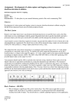
AN10850
LPC1700 timer triggered memory to GPIO data transfer
Rev. 01 — 16 July 2009
Application note
Document information
Info
Content
Keywords
LPC1700, GPIO, DMA, Timer0, Sleep Mode
Abstract
This application note briefly covers the functionality of the LPC1700 DMA
controller whilst performing a SRAM to GPIO DMA data transfer in
“Normal” and “Sleep” mode.
AN10850
NXP Semiconductors
GPIO DMA demo
Revision history
Rev
Date
Description
01
20090716
Initial version.
Contact information
For additional information, please visit: http://www.nxp.com
For sales office addresses, please send an email to: [email protected]
AN10850_1
Application note
© NXP B.V. 2009. All rights reserved.
Rev. 01 — 16 July 2009
2 of 10
AN10850
NXP Semiconductors
GPIO DMA demo
1. Introduction
This application note serves as a quick introduction to the LPC1700’s timer-triggered
DMA to GPIO functionality.
Without using a DMA (Direct Memory Access) controller, a data transfer between two
address locations is a multi-step process. Each step in this data transfer process requires
the CPU. Fortunately, one way to reduce the CPU’s overhead in transferring data is by
using a DMA controller. The DMA controller performs the tedious and repetitive tasks of
transferring data from one location to another.
Generally speaking, a DMA controller is hardware driven state machine with a sole
purpose to transfer data between memory and peripherals.
1.1 DMA
The LPC1700 features a DMA controller that has the ability to transfer data from
memory-to-memory, memory-to-peripheral, peripheral-to-peripheral, and peripheral-tomemory.
Using all eight of its channels, the DMA can transfer eight simultaneous 32-bit wide
words at a given time.
Some of the peripherals that are supported by the DMA include the SSP, I2S, UART, A/D
Converter, and the D/A Converter. For the DMA controller, the GPIO registers are
considered as “memory” sources/destinations. For example, to have the DMA copy data
from the internal SRAM to the GPIOs, it needs to be configured for a memory-to-memory
transfer.
The LPC1700’s DMA controller has scatter (or gather) support. This new feature allows
the DMA to transfer a non-contiguous block of memory with the guidance of a linked list
data structure.
1.2 GPIOs
The GPIO registers allow the user to utilize physical pins on the LPC1700 for regular I/O
purposes. On the LPC1700, these registers are located on an AHB peripheral bus for
fast I/O timing. They are byte, half-word, and word addressable. More importantly, the
LPC1700 GPIO registers are accessible by the DMA controller.
A detailed description of the GPIO registers and their features can be found in the
LPC1700 user manual.
1.3 Timers
The LPC1700 has four general purpose timers (Timer 0 to Timer 3). Each timer contains
four match registers (MR0 to MR3) that can generate interrupts and/or other actions,
such as stopping or resetting the timer’s counter register. Out of the four match registers
that each timer has, only the first two match registers (MR0 and MR1) are capable of
triggering a direct DMA request without using interrupts.
A detailed description of the timers and their features can be found in the LPC1700 user
manual. For demonstration purposes, we are just interested in a free-running timer and a
configured match register. More specifically, we are interested of having one of timer 0’s
match register trigger a DMA request directly to the DMA.
AN10850_1
Application note
© NXP B.V. 2009. All rights reserved.
Rev. 01 — 16 July 2009
3 of 10
AN10850
NXP Semiconductors
GPIO DMA demo
1.4 Power modes
The LPC1700 features several power modes so that the device’s current consumption
can be reduced. The power modes are:
• Normal Mode
• Sleep Mode
• Deep Sleep Mode
• Power-down Mode
• Deep Power-down Mode
The mode that we are particularly interested in is “Sleep” mode. To conserve power, the
LPC1700’s “Sleep” mode halts the clock to the CPU’s core and powers down the on-chip
flash. More importantly however, while the LPC1700 is in “Sleep” mode the peripheral
clocks and the SRAM memory module remain powered.
In other words, this means that during “Sleep” mode the LPC1700 stops executing
instructions to conserve power, but its DMA, SRAM, GPIOs and Timers still remain
active!
More details on the LPC1700’s power modes can be found in the LPC1700 user manual.
2. Application demo
2.1 Requirements
2.1.1 Hardware
Keil MCB1700 Development Board (See Fig 1).
Keil ULINK JTAG module
Note: Instead of using the ULINK JTAG module to program the LPC1700, you can use
an RS-232 serial cable along with the FlashMagic programming tool that is available at
no charge at http://www.nxp.com/redirect/flashmagictool.com/.
2.1.2 Software
Keil uVision3 Development IDE v3.7 or later (evaluation version will work for the demo).
The project demo is CMSIS (Cortex Microcontroller Software Interface Standard)
compliant.
2.2 Project design
In this project demo, we will use the DMA to transfer data that is located in SRAM to the
LEDs (GPIOs) on the MCB1700 development board. This is done by simply configuring
the DMA to make a memory-to-memory transfer every time when the match register for
Timer 0 matches its counter register. This DMA transfer can be demonstrated while the
CPU is in “Normal” or in “Sleep” mode.
The following sections elaborate on how the project demo is designed and structured.
AN10850_1
Application note
© NXP B.V. 2009. All rights reserved.
Rev. 01 — 16 July 2009
4 of 10
AN10850
NXP Semiconductors
GPIO DMA demo
2.2.1 Initialization and memory preparation
The LPC1700’s CPU is configured to run at 48 MHz, whereas Timer 0 runs at 24 MHz.
The GPIOs that are connected to the MCB1700 LEDs are configured as outputs. Fig 1
shows which LEDs and buttons are used throughout this project.
(1) LED and button configuration
Fig 1. Keil MCB1700
A block of unused memory is cleared and configured with known data. In this case we
will configure the SRAM to contain incrementing values. These values are then displayed
on the LEDs which are controlled by the DMA.
AN10850_1
Application note
© NXP B.V. 2009. All rights reserved.
Rev. 01 — 16 July 2009
5 of 10
AN10850
NXP Semiconductors
GPIO DMA demo
Fig 2. Memory configuration
2.2.2 Configuring the DMA request source
At this pointer, the Timer 0 match compare register is connected to the DMA so that it
can trigger a DMA request.
Fig 3. Selecting Timer 0’s match register to generate a DMA request
Once the DMA receives the DMA request from Timer 0, it will then transfer data from the
SRAM to the GPIO register that is connected to the MCB1700’s LEDs.
2.2.3 DMA configuration
With each DMA request, the DMA will automatically transfer the contents of the next
memory location until it has reached the last address specified in its DMA configuration.
(1) The DMA is configured to transfer data from SRAM to the LEDs
Fig 4. DMA configuration
AN10850_1
Application note
© NXP B.V. 2009. All rights reserved.
Rev. 01 — 16 July 2009
6 of 10
AN10850
NXP Semiconductors
GPIO DMA demo
2.2.4 Configure Timer 0 and enable
To make this project viewable, Timer 0 is configured so that it generates a DMA request
only two times a second. When the Timer 0 counter register matches its match register, it
resets the counter and toggles the match output signal.
Fig 5. Timer 0 configuration and enable
2.2.5 CPU LED toggle
While the DMA is enabled, the CPU can be in either one of two states. In “Normal” mode
it can loop in “while(1)” – toggling the LED at P1.28, or it can enter “Sleep” mode. In
“Sleep” mode P1.28 will stop toggling, whereas the DMA will continue until it has finished
the end of the entire data transfer.
To enter “Sleep” mode, press the “INT0” button.
(1) Pressing INT0 will cause the CPU to go into “Sleep” mode.
Fig 6. CPU toggling LED
AN10850_1
Application note
© NXP B.V. 2009. All rights reserved.
Rev. 01 — 16 July 2009
7 of 10
AN10850
NXP Semiconductors
GPIO DMA demo
2.3 Key observations
Note that the toggling rate of CPU controlled LED and the DMA controlled LEDs are
intentionally configured differently. A noticeable timing difference between the two sets of
LEDs indicates that the DMA is running independent from the CPU.
The overall objective of this project is to show that the:
1. DMA operates independently of the CPU, by showing different LED toggling rates.
2. DMA can transfer data to GPIO registers, by using LEDs.
3. Timers can generate DMA requests.
4. DMA continues to operate in “Sleep” mode.
3. Known issues
Keil’s uVision <LPC17xx.h> header file may not specify the “DMAREQSEL” register. To
fix this, open the LPC17xx.h header file that come with the uVision tool and ensure that
DMAREQSEL is put in the place indicated.
(1) DMAREQSEL may not be defined already
Fig 7. “LPC17xx.h” header file placeholder
AN10850_1
Application note
© NXP B.V. 2009. All rights reserved.
Rev. 01 — 16 July 2009
8 of 10
AN10850
NXP Semiconductors
GPIO DMA demo
4. Legal information
4.1 Definitions
Draft — The document is a draft version only. The content is still under
internal review and subject to formal approval, which may result in
modifications or additions. NXP Semiconductors does not give any
representations or warranties as to the accuracy or completeness of
information included herein and shall have no liability for the consequences
of use of such information.
to result in personal injury, death or severe property or environmental
damage. NXP Semiconductors accepts no liability for inclusion and/or use of
NXP Semiconductors products in such equipment or applications and
therefore such inclusion and/or use is for the customer’s own risk.
Applications — Applications that are described herein for any of these
products are for illustrative purposes only. NXP Semiconductors makes no
representation or warranty that such applications will be suitable for the
specified use without further testing or modification.
Export control — This document as well as the item(s) described herein
may be subject to export control regulations. Export might require a prior
authorization from national authorities.
4.2 Disclaimers
General — Information in this document is believed to be accurate and
reliable. However, NXP Semiconductors does not give any representations
or warranties, expressed or implied, as to the accuracy or completeness of
such information and shall have no liability for the consequences of use of
such information.
4.3 Trademarks
Notice: All referenced brands, product names, service names and
trademarks are property of their respective owners.
Right to make changes — NXP Semiconductors reserves the right to make
changes to information published in this document, including without
limitation specifications and product descriptions, at any time and without
notice. This document supersedes and replaces all information supplied prior
to the publication hereof.
Suitability for use — NXP Semiconductors products are not designed,
authorized or warranted to be suitable for use in medical, military, aircraft,
space or life support equipment, nor in applications where failure or
malfunction of a NXP Semiconductors product can reasonably be expected
AN10850_1
Application note
© NXP B.V. 2009. All rights reserved.
Rev. 01 — 16 July 2009
9 of 10
AN10850
NXP Semiconductors
GPIO DMA demo
5. Contents
1.
1.1
1.2
1.3
1.4
2.
2.1
2.1.1
2.1.2
2.2
2.2.1
2.2.2
2.2.3
2.2.4
2.2.5
2.3
3.
4.
4.1
4.2
4.3
5.
Introduction .........................................................3
DMA ...................................................................3
GPIOs ................................................................3
Timers ................................................................3
Power modes .....................................................4
Application demo ................................................4
Requirements.....................................................4
Hardware............................................................4
Software .............................................................4
Project design ....................................................4
Initialization and memory preparation ................5
Configuring the DMA request source .................6
DMA configuration..............................................6
Configure Timer 0 and enable............................7
CPU LED toggle.................................................7
Key observations................................................8
Known issues ......................................................8
Legal information ................................................9
Definitions ..........................................................9
Disclaimers.........................................................9
Trademarks ........................................................9
Contents.............................................................10
Please be aware that important notices concerning this document and the product(s)
described herein, have been included in the section 'Legal information'.
© NXP B.V. 2009. All rights reserved.
For more information, please visit: http://www.nxp.com
For sales office addresses, email to: [email protected]
Date of release: 16 July 2009
Document identifier: AN10850_1