1
Lab 1: A “Blinky” Introduction to C and Assembly Programming
EE-379 Embedded Systems with Applications
Electrical Engineering Department, University at Buffalo
Last update: Cristinel Ababei, January 2013
1. Objective
The objective of this lab is to give you a “first foot in the door” exposure to the programming in C and
assembly of a program, which when executed by the microcontroller (NXP LPC1768, an ARM Cortex-M3)
simply blinks LEDs located on the development board. You also learn how to use the ARM Keil uVision
IDE to create projects, build and download them to the board (either Keil MCB1700 or Embest EMLPC1700).
2. Pre-lab Preparation
Optional (but encouraged)
You should plan to work on your own computer at home a lot during this semester. You should install the
main software (evaluation version) we will use in this course: the Microcontroller Development Kit (MDKARM), which supports software development for and debugging of ARM7, ARM9, Cortex-M, and Cortex-R4
processor-based devices. Download it from ARM’s website [1] and install it on your own computer. This is
already installed on the computers in the lab.
MDK combines the ARM RealView compilation tools with the Keil µVision Integrated Development
Environment (IDE). The Keil µVision IDE includes: Project Management and Device & Tool
Configuration, Source Code Editor Optimized for Embedded Systems, Target Debugging and Flash
Programming, Accurate Device Simulation (CPU and Peripheral).
You should read this lab entirely before attending your lab session. Equally important, you should/browse
related documents suggested throughout the description of this lab. These documents and pointers are
included either in the downloadable archive for this lab or in the list of References. Please allocate
significant amount of time for doing this.
3. Lab Description
3.1 BLINKY 1
Creating a new project
1. First create a new folder called say EE378_S2013 where you plan to work on the labs of this course.
Then, inside it, create a new folder called lab1.
2. Launch uVision4, Start->All Programs->Keil uVision4
3. Select Project->New uVision Project… and then select lab1 as the folder to save in; also type blinky1
as the File Name.
4. Then, select NXP (founded by Philips) LPC1768 as CPU inside the window that pops-up. Also, click
Yes to Copy “startup_LPCxx.s” to Project Folder.
5. Under File Menu select New.
6. Write your code in the and save it as blinky1.c in the same project folder. This file (as well as all others
discussed in this lab) is included in the downloadable archive from the website of this course. The panel
1
7.
8.
9.
10.
11.
12.
13.
14.
on the left side of the uVision IDE is the Project window. The Project window gives you the hierarchy
of Target folder and Source Group folder.
Right click on the “Source Group 1” and select “Add files to Source Code”.
Locate blinky1.c and include it to the group folder.
Copy C:\Keil\ARM\Startup\NXP\LPC17xx\system_LPC17xx.c to lab1 directory and add it as a
source file to the project too. Open this file and browse it quickly to see what functions are defined
inside it.
Click Project menu and then select Build Target.
Build Output panel should now show that the program is being compiled and linked. This creates
blinky1.axf file (in ARM Executable Format), which will be downloaded to the board. To create a .hex
file (more popular), select Flash->Configure Flash Tools->Output and check mark Create HEX File.
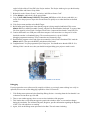
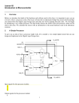
Connect the board to two USB ports of the host computer. One connection is to the port J16 of the
board (the one that is a Standard-B plug). The second connection is via the ULINK2
debugger/programmer/emulator. These connections are illustrated in Fig.1.
Download the program to the Flash of the microcontroller. Select Flash->Download. This loads the
blinky1.axf file. Then press the RESET push-button of the board.
Congratulations! You just programmed your first project. You should notice that the LED P1.29 is
blinking. If this is not the case, then you should investigate/debug your project to make it work.
Figure 1 Connection of ULINK2 to the board.
Debugging
If your program has errors (discovered by compiler or linker) or you simply want to debug it to verify its
operation, then we can use the debugging capabilities of the uVision tools.
1. Click Debug menu option and select Start/Stop Debug Session. A warning about the fact that this is an
evaluation version shows up; click OK.
2. Then, a new window appears where we can see the simulation of the program.
3. This window has several different supportive panels/sub-windows where we can monitor changes
during the simulation. The left hand side panel, Registers, provides information regarding the Registers
of LPC17xx with which we are working.
4. Again, click on the Debug menu option and select Run. The code starts simulating.
2
5. It is good practice that before going ahead with the actual hardware implementation to perform a
debug/simulation session to make sure that our program behaves according to the design requirements.
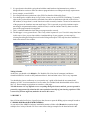
6. In our example, we use PORT1.
7. Go to Peripherals menu option then select GPIO Fast Interface followed by Port 1.
8. You should get the window shown in Fig.2 below, where you can see LED P1.29 blinking. To actually
observe this you should wait until the simulated time (shown on the bottom-right side of the uVision
ISE window) is longer than 1 second. Note that in order to actually simulate 1 second of execution time
of the program, the simulator must run much longer. This is expected, as typically simulators require
much longer computational runtimes (wallclock time) in order to simulate relatively short execution
times of the program under investigation!
9. This is a standard method to check that your program works correctly.
10. The debugger is a very powerful tool. This is only a brief exposure to it; we’ll revisit it many times later
in this course. Once you are done with the simulation/debug of your program, you can stop it by
selecting Start/Stop the Debug Session from the Debug menu option. This stops the show and takes us
back to the main uVision window.
Figure 2 Pin P1.29 is checked on/off every other second or so.
Taking it further
At this time, you should revisit blinky1.c file. Read this file (it has lots of comments) and browse
related/included files in order to fully understand what is what and what it does. This is very important.
You should take time to read/browse on your own the user’s guide of the board, the user manual and
datasheet of LPC17xx microcontrollers as well as other files included in the downloadable archive of this
lab [2-5]. Do not attempt to print them as some have >800 pages.
Note that because it is very difficult to cover everything during the lectures and labs, you are expected to
proactively engage materials related to this course and take ownership of your learning experience! This
is a necessary (but not sufficient) attitude to do well in this course.
3.2 BLINKY 2
Start uVision and select Project->Open Project, then, browse to open the Blinky project example located at:
C:\Keil460\ARM\Boards\Keil\MCB1700\Blinky
As you noticed, the ARM Kiel software installation contains a folder called Boards that contains design
examples for a variety of boards. We’ll use some of these design examples for the board utilized in this
3
course. However, as we go, you should take a look and play with all these examples; try to understand their
code.
Build the project and download to target. Observe operation and comment.
At this time, you should take time to read the .c files of this project, starting with Blinky.c. Read it and also
browse the other files to gain insights into what and how the code achieves different tasks. At this stage, do
not expect to understand everything; however, please make an effort to see as much as you can.
3.3 BLINKY 3
In this part of the lab, we implement the blinky example by writing a program in assembly language. In this
example we’ll turn on/off the LED controlled by pin P1.28. Start uVision and create a new project. Add to
it the following files:
1. When creating the project say Yes to have added startup_LPCxx.s to the project
2. blinky3.s (available in the downloadable archive of this lab as well in an ppendix at the end of this lab)
3. C:\Keil\ARM\Startup\NXP\LPC17xx\system_LPC17xx.c. This is needed for the SystemInit()
function called from within startup_LPCxx.s. We could not add this file to the project provided that
we comment out the two lines inside startup_LPCxx.s that contain SystemInit.
Build the project and download to target. Observe operation and comment.
At this time, you should take time to read the blinky3.s. Read it and make sure you understand how the
code achieves each task.
4. Lab Assignment
Modify the assembly program blinky3.s to implement the following design description: blink all eight
LEDs on the board, one by one from left to right repeatedly.
For each lab with a “Lab Assignment”, you must turn-in a lab report in PDF format (font size 11, single
spacing), named lab#_firstname_lastname.pdf (where “#” is the number of the lab, for example in the
case of lab1, “#” must be replaced with 1) which should contain the following sections:
Lab title, Your name
Introduction section – a brief description of the problem you solve in this lab assignment, outlining the
goal and design requirements.
Solution section – describe the main technique(s) that you utilized to develop your solution. Include
block diagrams, flow graphs, plots, etc. here to aid your explanation.
Results and Conclusion section – describe your results and any issues you may have faced during the
assignment and how you solved them.
Code listings, assembly or C code that you wrote. Appended at the end of your report. Use smaller font
(size 9) to save space.
For full credit, you must demo the correct operation of your assignment to the TA during the next lab.
While you are free to hand-write your report (still turned-in as a PDF file), please make sure your report is
neat and the presentation is coherent. You will lose points for reports that do not present enough details, are
ugly, disorganized, or are hard to follow/read.
4
5. Credits and references
[1] Software: Microcontroller Development Kit; download from http://www.keil.com/arm/mdk.asp
[2] Hardware: MCB1700 board User’s Guide;
http://www.keil.com/support/man/docs/mcb1700/mcb1700_su_connecting.htm
[3] LPC17xx user’s manual; http://www.nxp.com/documents/user_manual/UM10360.pdf
[4] NXP LPC17xx datasheet;
http://www.nxp.com/documents/data_sheet/LPC1769_68_67_66_65_64_63.pdf
http://www.keil.com/dd/chip/4868.htm
[5] Cortex-M3 information;
http://www.nxp.com/products/microcontrollers/cortex_m3/
http://www.arm.com/products/processors/cortex-m/cortex-m3.php
[6] Additional resources
--Keil uVision User’s Guide
http://www.keil.com/support/man/docs/uv4/
-- Keil uVision4 IDE Getting Started Guide
www.keil.com/product/brochures/uv4.pdf
--ARM Assembler Guide
http://www.keil.com/support/man/docs/armasm/
--ARM Compiler toolchain for uVision. Particularly browse:
ARM Compiler toolchain for uVision, Using the Assembler
ARM Compiler toolchain for µVision, Using the Linker
http://infocenter.arm.com/help/index.jsp?topic=/com.arm.doc.dui0377c/index.html
--Professor J.W. Valvano (UTexas) resources;
http://users.ece.utexas.edu/~valvano/Volume1/uvision/
--UWaterloo ECE254, Keil MCB1700 Hardware Programming Notes
https://ece.uwaterloo.ca/~yqhuang/labs/ece254/doc/MCB1700_Hardware.pdf
----EE 472 Course Note Pack, Univ. of Washington, 2009,
http://abstract.cs.washington.edu/~shwetak/classes/ee472/notes/472_note_pack.pdf (Chapter 6)
APPENDIX A: Some info on LPC1768 peripherals programming
Pins on LPC1768 are divided into 5 ports indexed from 0 to 4. Pin naming convention is Px.y, where x is
the port number and y is the pin number. For example, P1.29 means Port 1, Pin 29. Each pin has four
operating modes: GPIO (default), first alternate function, second alternate function, and third alternate
function. Any pin of ports 0 and 2 can be used to generate an interrupt.
To use any of the LPC1768 peripherals, the general steps to be followed are:
1. Power Up the peripheral to be used
2. Set the Clock Rate for the peripheral
3. Specify the pin operating mode - Connect necessary pins using Pin Connect Block
4. Set direction - Initialize the registers of the peripheral
1. Power Up the peripheral
5
Let’s assume we are interested in utilizing the pin P1.29 to drive one of the board’s LEDs on and off
(the blinky1 example). Refer to LPC17xx User’s Manual, Chapter 4: Clocking and Power Control.
Look for register Power Control for Peripherals register, PCONP. It’s on page 63; bit 15 is PGPIO.
Setting this bit to 1 should power up the GPIO ports. Note that the default value is 1 anyway, which
means GPIO ports are powered up by default on reset; but the start up code may modify this. Hence,
it’s good practice to make sure we take care of it. For example, here is how we power up the GPIO:
LPC_SC->PCONP |= 1 << 15;
2. Set desired clock to the peripheral
In the same Chapter 4 of the manual, look for Peripheral Clock Selection register, PCLKSEL1; it's on
page 57; bits 3:2 set the clock divider for GPIO. In our example, since we're not using interrupts, we
won’t change the default value. Note that PCLK refers to Peripheral Clock and CCLK refers to CPU
Clock. PCLK is obtained by dividing CCLK; see table 42 on page 57 of the manual;
3. Specify the pin operating mode - Connect necessary pins using Pin Connect Block
To specify the pin operating mode we configure PINSEL registers in the Pin Connect
Block(LPC_PINCON macro defined in LPC17xx.h). There are eleven PINSEL registers: PINSEL0,
PINSEL1, …, PINSEL10, which are defined as member variables inside the LPC_PINCON_TypeDef
C struct. Each one of these eleven registers controls a specific set of pins on a certain port. When the
processor powers up or resets, the pins that are connected to the LEDs and joystick are automatically
configured as GPIO (default). Hence, in our example, there is no need to change settings in the pin
connect block. However, it is a good practice to configure these pins before using them.
Refer to Section 8.1 of LPC17xx user’s manual to see which set of pins are controlled by which
PINSEL register. As an example, the five button joystick is connected to pins P1.20, P1.23, P1.24,
P1.25 and P1.26. As mentioned earlier, it is a good programming practice to configure it. Refer to page
109, Section 8.5.4, Table 82 in LPC17xx User’s Manual for more detailed information.
LPC_PINCON->PINSEL3 &= ~((3<< 8)|(3<<14)|(3<<16)|(3<<18)|(3<<20));
// P1.20, P1.23, …, P1.26 are GPIO (Joystick)
4. Set direction - Initialize the registers of the peripheral
In this step of programming of a GPIO pin, we set the I/O direction (i.e., pin to be used as input or
output). This is done via FIODIR register (see Chapter 9, page 122 of LPC17xx User’s Manual for
more info). There are five LPC_GPIOx, where x=0,1,2,3,4, macros defined in LPC17xx.h. The FIODIR
is a member variable in LPC_GPIO_TypeDef C struct in LPC17xx.h. To set a pin as input, set the
corresponding bit in FIODIR to 0. All I/Os default to input (i.e., all bits in FIODIR are default to logic
0). To set a pin as output, set the corresponding bit in FIODIR to 1. For example, to set pins connected
to the joystick as input, we write the following C code:
LPC_GPIO1->FIODIR &= ~((1<<20)|(1<<23)|(1<<24)|(1<<25)|(1<<26));
// P1.20, P1.23, ..., P1.26 are input (Joystick)
In our blinky example, we set all pins connected to the 8 LEDs as output. We achieve that via the
following C code:
LPC_GPIO1->FIODIR |= 0xB0000000; // pins P1.28, P1.29, P1.31 as output
6
LPC_GPIO2->FIODIR |= 0x0000007C; // pins P2.2, 3, 4, 5, 6 as output
Once a pin is set as output or input it can be utilized in our programs to drive or read logic values.
a) The pin is set as output
We turn a pin to HIGH/LOW (i.e., digital logic 1/0) by setting the corresponding bit in
FIOSET/FIOCLR register. Both FIOSET and FIOCLR are member variables defined in the
PC_GPIO_TypeDef C struct. To set a pin to digital 1, set the corresponding bit of LPC_GPIOx>FIOSET to 1. To turn a pin to digital 0, set the corresponding bit of LPC_GPIOx->FIOCLR to 1.
Refer to Sections 9.5.2 and 9.5.3 of LPC17xx User’s manual for details.
For example, to turn on LED P1.29, the following code can be used:
LPC_GPIO1->FIOSET = 1 << 29;
In general, to turn any of the 8 LEDs on, one can use the following trick:
const U8 led_pos[8] = { 28, 29, 31, 2, 3, 4, 5, 6 };
mask = 1 << led_pos[led];
if (led < 3) { // P1.28,29,31 are part of Port1
LPC_GPIO1->FIOSET = mask;
} else { // P2.2,3,4,5,6 are part of Port2
LPC_GPIO2->FIOSET = mask;
}
Of course, to turn off a particular LED, just replace FIOSET with FIOCLR in the above code.
Note: we can also set HIGH/LOW a particular output pin via the FIOPIN register. We can write
specific bits of the FIOPIN register to set the corresponding pin to the desired logic value. In this
way, we bypass the need to use both the FIOSET and FIOCLR registers. However, this is not the
recommended method. For example, in the case of the blinky example, we use the following C code:
LPC_GPIO1->FIOPIN |= 1 << 29; // make P1.29 high
LPC_GPIO1->FIOPIN &= ~( 1 << 29 ); // make P1.29 low
b) The pin is set as input
We read the current pin state from FIOPIN register. The corresponding bit being 1 indicates that the
pin is driven high. The corresponding bit being 0 indicates that the pin is driven low. The FIOPIN is
a member variable defined in LPC_GPIO_TypeDef C struct. One normally uses bit shift operations
to shift the LPC_GPIOx->FIOPIN value to obtain pin value(s). Refer to Section 9.5.4 in the
LPC17xx User’s manual for details. For example, to read the joystick position, the following code
can be used
#define KBD_MASK 0x79
uint32_t kbd_val;
kbd_val = (LPC_GPIO1->FIOPIN >> 20) & KBD_MASK;
When the joystick buttons are inactive, the bits located at P1.23,24,25,26 are logic 1. When any of
the joystick buttons becomes active, the bit corresponding to that pin becomes 0.
7
APPENDIX B: Listing of blinky3.s
; CopyLeft (:-) Cristinel Ababei, SUNY at Buffalo, 2012
; this is one assembly implementation of the infamous blinky example;
; target microcontroler: LPC1768 available on board Keil MCB1700 (or Embest EM-LPC1700 board)
; I tested it first on EM-LPC1700 board as it's cheaper!
;
; Note1: it has lots of comments, as it is intended for the one who
; sees for the first time assembly;
; Note2: some parts of the implementation are written in a more complicated manner
; than necessary for the purpose of illustrating for example different memory
; addressing methods;
; Note3: each project will have to have added to it also system_LPC17xx.s (added
; automatically by Keil uVision when you create your project) and system_LPC17xx.c
; which you can copy from your install directory of Keil IDE (for example,
; C:\Keil\ARM\Startup\NXP\LPC17xx\system_LPC17xx.c)
; Note4: system_LPC17xx.s basically should contain the following elements:
; -- defines the size of the stack
; -- defines the size of the heap
; -- defines the reset vector and all interrupt vectors
; -- the reset handler that jumps to your code
; -- default interrupt service routines that do nothing
; -- defines some functions for enabling and disabling interrupts
; Directives
; they assist and control the assembly process; directives or "pseudo-ops"
; are not part of the instruction set; they change the way the code is assembled;
; THUMB directive placed at the top of the file to specify that
; code is generated with Thumb instructions;
THUMB
; some directives define where and how the objects (code and variables) are
; placed in memory; here is a list with some examples:
; AREA, in assembly code, the smallest locatable unit is an AREA
; CODE is the place for machine instructions (typically flash ROM)
; DATA is the place for global variables (typically RAM)
; STACK is the place for the stack (also in RAM)
; ALIGN=n modifier starts the area aligned to 2^n bytes
; |.text| is used to connect this program with the C code generated by
; the compiler, which we need if linking assembly code to C code;
; it is also needed for code sections associated with the C library;
; NONINT defines a RAM area that is not initialized (normally RAM areas are
; initialized to zero); Note: ROM begins at 0x00000000 and RAM begins at
; 0x2000000;
; EXPORT is a directive in a file where we define an object and
; IMPORT directive is used in a file from where we wish to access the object;
; Note: we can export a function in an assembly file and call the function
; from a C file; also, we can define a function in C file, and IMPORT the function
; into an assembly file;
; GLOBAL is a synonym for EXPORT
; ALIGN directive is used to ensure the next object is aligned properly; for example,
; machine instructions must be half-word aligned, 32-bit data accessed with LDR, STR
; must be word-aligned; good programmers place an ALIGN at the end of each file so the
; start of every file is automatically aligned;
; END directive is placed at the end of each file
; EQU directive gives a symbolic name to a numeric constant, a register-relative
8
; value or a program-relative value; we'll use EQU to define I/O port addresses;
AREA |.text|, CODE, READONLY ; following lines are to be placed in code space
EXPORT
__main
ENTRY
; EQUates to make the code more readable; to turn LED P1.28 on and off
; we will write the bit 28 of the registers FIO1SET (to set HIGH) and FIO1CLR (to set LOW);
; refer to page 122 of the LPC17xx user manual to see the adresses of these registers; they are:
FIO1SET
EQU 0x2009C038
FIO1CLR
EQU 0x2009C03C
; we will implement a dirty delay by decrementing a large enough
; number of times a register;
LEDDELAY EQU 10000000
__main
; (1) we want to set as output the direction of the pins that
; drive the 8 LEDs; these pins belong to the ports Port 1 and Port 2
; and are: P1.28, P1,29, P1.31 and P2.2,...,6
; to set them as output, we must set to 1 the corresponding bits in
; registers (page 122 of LPC17xx user manual):
; FIO1DIR - 0x2009C020
; FIO2DIR - 0x2009C040
; that is, we'll set to 1 bits 28,29,31 of the register at adress 0x2009C020,
; which means writing 0xB0000000 to this location; also, we'll set 1 bits 2,...,6
; of the register at address 0x2009C040, which means writing 0x0000007C to
; this location;
MOV R1, #0x0 ; init R1 register to 0 to "build" address
MOVT R1, #0x2009 ; assign 0x20090000 to R1; MOVT assigns to upper nibble
MOV R3, #0xC000 ; move 0xC000 into R3
ADD R1, R1, R3 ; add 0xC000 to R1 to get 0x2009C000
MOV R4, #0xB0000000 ; place 0xB0000000 (i.e., bits 28,29,31) into R4
; now, place contents of R4 (i.e. 0xB0000000) to address
; 0x2009C020 (i.e., register FIO1DIR); this sets pins
; 28,29,31 as output direction;
; Note: address is created by adding the offset 0x20 to R1
; Note: the entire complication above could be replaced with
; simply loading R1 with =FIO1DIR (but we wanted to experiment with
; different flavors of MOV, to upper and lower nibbles); we'll use
; the simpler version later;
STR R4, [R1, #0x20]
MOV R4, #0x0000007C ; value to go to register of Port 2
STR R4, [R1, #0x40] ; set output direction for pins of Port 2 by writing to reister FIO2DIR
; (2) set HIGH the LED driven by P1.28; to do that we load current
; contents of register FIO1SET (i.e., memory address 0x2009C038) to R3,
; set to 1 its 28th bit, and then put it back into the location at
; memory address 0x2009C038 (i.e., effectively writing into register FIO1SET);
LDR R1, =FIO1SET ; we'll not touch R1 anymore so that it keeps this address
LDR R3, [R1]
ORR R3, #0x10000000 ; set to logic 1 bit 28 of R3
STR R3, [R1]
; (3) some initializations
LDR R0, =LEDDELAY ; initialize R0 for countdown
LDR R2, =FIO1CLR ; we'll not touch R2 anymore so that it keeps this address
; now, the main thing: turn the LED P1.28 on and off repeatedly;
; this is done by setting the bit 28 of registers FIO1CLR and FIO1SET;
9
; Note: one could do this in a simpler way by using a toggling trick:
; toggle (could be done using exclusive or with 1) bit 28 of register
; FIO1PIN instead (page 122 of LPC17xx user manual) and not use
; FIO1CLR and FIO1SET; I do not recommend however this trick as
; due to the peculiarities of FIO1PIN;
loop
led_on
SUBS R0, #1 ; decrement R0; this sets N,Z,V,C status bits
BNE led_on ; if zero not reached yet, go back and keep decrementing
LDR R3, [R2] ; recall that R2 stores =FIO1CLR
ORR R3, #0x10000000 ; set to logic 1 bit 28 of R3
STR R3, [R2] ; place R3 contents into FIO1CLR, which will put pin on LOW
LDR R0, =LEDDELAY ; initialize R0 for countdown
led_off
SUBS R0, #1 ; decrement R0; this sets N,Z,V,C status bits
BNE led_off ; if zero not reached yet, go back and keep decrementing
LDR R3, [R1] ; recall that R1 stores =FIO1SET
ORR R3, #0x10000000 ; set to logic 1 bit 28 of R3
STR R3, [R1] ; place R3 contents into FIO1SET, which will put pin on HIGH
LDR R0, =LEDDELAY ; initialize R0 for countdown
; now do it again;
B loop
ALIGN
END
10