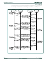
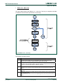
1
UM0801-03 PN533 User Manual Rev. 03 User Manual Document information Info Content Keywords NFC, PN533, V2.7 Abstract This document describes the firmware V2.7 embedded in the PN533. UM0801-03 NXP Semiconductors PN533 User Manual Revision history 01 2008-04-01 Initial version for firmware version V2.6 (PN533) 02 2008-07-31 Update the user manual for the firmware version V2.7 (PN533) 03 2009-01-14 Perform some corrections in the User Manual. This UM is applicable for the firmware version V2.7 (PN533) Contact information For additional information, please visit: http://www.nxp.com For sales office addresses, please send an email to: [email protected] UM0801-03 User Manual © NXP B.V. 2008. All rights reserved. Rev. 03 - 14 January 2009 2 of 175 UM0801-03 NXP Semiconductors PN533 User Manual 1. Introduction 1.1 Purpose and Scope The PN533 is a highly integrated transmission module for contactless communication at 13.56 MHz including microcontroller functionality based on an 80C51 core with 44 Kbytes of ROM and 1232 bytes of RAM. The PN533 combines a modulation and demodulation concept completely integrated for different kinds of contactless communication methods and protocols at 13.56 MHz with an easy-to-use firmware for the different supported modes and the USB host controller interface. This document describes the firmware embedded in the PN533 chip, in particular the global behavior in the system depending if the PN533 device is used as initiator or target. 1.2 Intended audience This document has been written to allow the use of the PN533 from the host controller point of view. All the RF protocols used by the PN533 are not described in this document. The reader is supposed to have knowledge on NFCIP-1 (Reference [3]) and ISO/IEC14443 (Reference [1] & [2]). 1.3 Glossary APDU Application Protocol Data Unit ATQA Answer To Request, type A ATQB Answer To Request, type B C-APDU Command APDU CIU Contactless Interface Unit CL ContactLess CPU Central Processing Unit CT Cascade Tag DEP ISO/IEC18092 Data Exchange Protocol DRI Bit duration of Target to Initiator DSI Bit duration of Initiator to Target E.S.M Energy Saving Mode FSL Maximum value for the Frame Length I2C Inter Integrated Circuit IC Integrated Circuit ID Card Identifier N/A Not Applicable NAD Node ADdress NFC-SEC NFC Secure N/I Not Implemented NU Not Used PCB Protocol Control Byte (ISO/IEC14443-4) UM0801-03 User Manual © NXP B.V. 2008. All rights reserved. Rev. 03 - 14 January 2009 3 of 175 UM0801-03 NXP Semiconductors PN533 User Manual PCD Proximity Coupling Device (Contactless PCD) PFB Control Information for Transaction (NFCIP-1) PPS Protocol and Parameter Selection R-APDU Response APDU RATS Request for Answer To Select RFA Radio Frequency Activation RFU Reserved for Future Use SDD Single Device Detection SEP Secure Exchange Protocol SRS Software Requirements Specification TBD To Be Defined TLV Encoding method (Type, Length, Value) TPE NFC Transport Protocol Equipped (DEP.Data Exchange Protocol) TSN Time Slot Number T=CL ISO/IEC14443-4 protocol UID Unique Identifier, Type A UM0801-03 User Manual © NXP B.V. 2008. All rights reserved. Rev. 03 - 14 January 2009 4 of 175 UM0801-03 NXP Semiconductors PN533 User Manual 1.4 References [1] ISO/IEC 14443-3 Identification cards – Contactless integrated circuit(s) cards Proximity card(s) Part 3: Initialization and anti-collision [2] ISO/IEC 14443-4 Identification cards – Contactless integrated circuit(s) cards Proximity card(s) Part 4: Transmission protocol [3] ISO/IEC 18092 1 Near Field Communication - Interface and Protocol (NFCIP-1) [4] PN533/C1 Product Datasheet PN533 NFC Controller Product data sheet [5] AN10682_2 PN533 Application Note [6] AN010207-4 Smart Card Reader Application with TDA8029 [7] NFC-PRIV-P2P Privacy feature for NFCIP-1 for Peer-to-Peer Communication [8] Paypass 1.1 Paypass - ISO/IEC 14443 Implementation Specification 1.1 [9] EMVco 2.0 EMV Contactless Specifications for Payment Systems 2.0 [10] USB 2.0 Universal Serial Bus Specification revision 2.0 [11] I2C 3.0 I²C bus Specification revision 3.0 1 Purchase of an NXP Semiconductors IC that complies with one of the NFC Standards (ISO/IEC18.092;ISO/IEC21.481) does not convey an implied license under any patent right on that standards. A license for the portfolio of the NFC Standards patents of NXP B.V. needs to be obtained at Via Licensing, the pool agent of the NFC Patent Pool, e-mail: [email protected]. UM0801-03 User Manual © NXP B.V. 2008. All rights reserved. Rev. 03 - 14 January 2009 5 of 175 UM0801-03 NXP Semiconductors PN533 User Manual 1.5 General presentation of the PN533 • The embedded firmware and the internal hardware support the handling of the host controller protocol for USB interface. The host controller protocol is defined in chapter 7 (p.34). The firmware of the PN533 supports the following operating modes: • PCD mode for FeliCa (212 kbps & 424 kbps), ISO/IEC14443 Type A & B (from 106 kbps to 847 kbps), MIFARE (106 kbps), RFA cards (106 kbps) and Innovision Jewel cards (106 kbps). • NFC IP-1 (with NFC Secure compliancy) mode. The NFC IP-1 mode offers different baud rates from 106 kbps up to 424 kbps. The PN533 handles the complete NFC framing and error detection. • The PN533 manages an I2C master interface. The PN533 is configured as master and is able to communicate with external EEPROM (address 0xA0) and a smart card reader (TDA8029). • PN533 in PCD mode is compliant with Paypass specification V1.1 and EMV contactless specification V2.0. In this document: • PN533 refers to PN533/V2.7. UM0801-03 User Manual © NXP B.V. 2008. All rights reserved. Rev. 03 - 14 January 2009 6 of 175 UM0801-03 NXP Semiconductors PN533 User Manual 2. Configuration Modes The PN533 has 3 possible modes that can be chosen by using two GPIOs during the reset phase of the IC: Table 1. Configuration modes Selection Pins Mode P70_IRQ (pin #21) P35 (pin #20) 1 1 0 0 PN512 emulation 1 0 RF field ON 0 1 Standard 2.1 Standard Mode This is the default mode of the PN533. The description of this mode is detailed in this document starting from chapter 3 (p.9). 2.2 PN512 emulation mode In this test mode, the PN533 is configured to act as real PN512 IC using serial interface. The PN512 is a transmission module for contactless communication at 13.56 MHz. It integrates a modulation and demodulation concept for different kind of contactless communication methods and protocols. Then, the PN533 can be easily interfaced with the PN512 dedicated host controller software, as e.g. Joiner PC Serial. The link used is RS232 at 9600 bauds 2 . It is not possible to change the value of the baud rate; the SerialSpeedReg register is not emulated. The emulation of the PN512 IRQ pin is supported as well; the pin used is P70_IRQ. The level of the P70_IRQ pin is low when an interrupt occurs. The bit IRQInv in the register CommIEnReg has no effect (see [4]). 2 The RS232 link used here is the standard UART, not the High Speed UART. Consequently, in this mode the PN533 must be interconnected with P30 (pin#24) for the RS232_RX line and P31 (pin#31) for the RS232_TX line. UM0801-03 User Manual © NXP B.V. 2008. All rights reserved. Rev. 03 - 14 January 2009 7 of 175 UM0801-03 NXP Semiconductors PN533 User Manual 2.3 RFfieldON Mode In this mode, the PN533 is configured to switch on its RF field immediately after the reset. The modulation and the baud rate used depend on the selection GPIOs P33_INT1 and P34/SIC_CLK and random data bytes are continuously sent. In this mode, the temperature sensor is not activated, so that tests can be done at temperature higher than 125°C. Table 2. TX framing and TX speed in RFfieldON configuration Selection Pins TX framing – TX speed P33_INT1 (pin #33) P34/SIC_CLK (pin #34) 1 1 0 0 FeliCa - 212 kbps 0 1 FeliCa - 424 kbps 1 0 MIFARE - 106 kbps UM0801-03 User Manual © NXP B.V. 2008. All rights reserved. Rev. 03 - 14 January 2009 8 of 175 UM0801-03 NXP Semiconductors PN533 User Manual 3. Power management The design of the firmware embedded in the PN533 takes care of power consumption, in a sense that it minimizes the overall power consumption. This chapter defines the strategy used to save current consumption. The firmware can play with different parameters described hereafter: • Power modes of the CPU, • Power modes of the CL front-end, • Management of pin configuration. UM0801-03 User Manual © NXP B.V. 2008. All rights reserved. Rev. 03 - 14 January 2009 9 of 175 UM0801-03 NXP Semiconductors PN533 User Manual 3.1.1 Power modes of the PN533 The PN533 has different power modes which are listed in the following table (refer to [4] to have a complete description). 3.1.1.1 Power modes for CPU Table 3. Power modes for CPU Power Mode Description Hard Power Down The CPU is in reset state. This mode can be reached only by an external action on RSTPDN pin, not by a firmware action. Normal The CPU is running. Power Down Oscillator is stopped, needs delay to be waken up (typ. 500µs). 3.1.1.2 Power modes for Contact Less interface Table 4. Power modes for CL interface Power Mode Description Hard Power Down The contactless UART and the analog front end are in reset state. This mode can be reached only by external action on RSTPDN pin, not by a firmware action. The contactless UART is running. CL_A The analog front end is operational. RF field is not generated. The contactless UART is running. CL_B The analog front end is operational. RF field is generated. The contactless UART is in Power Down mode. CL_C The analog front end is partially operational (only the RF level detector is active). RF field is not generated. The contactless UART and the analog front end are set in the mode in which the power consumption is the minimum, i.e. power down with RF level detector not activated. CL_D 3.1.1.3 Power modes for the TDA8029 Table 5. Power modes for the TDA8029 Power Mode Description Hard Power Down The TDA8029 is in reset state Shutdown The CPU of the TDA8029 is set in powerdown mode. Normal The TDA8029 is running UM0801-03 User Manual © NXP B.V. 2008. All rights reserved. Rev. 03 - 14 January 2009 10 of 175 UM0801-03 NXP Semiconductors PN533 User Manual 3.1.2 Operating modes of the PN533 3.1.2.1 Mode dispatcher The firmware adapts the overall power consumption to the real needs depending on the state where it is. Several cases have to be considered; the power modes involved being different: • Standby mode, • Initiator / PCD mode, • Target mode. The transition between the three defined modes is automatically done by the firmware, either due to a change in the internal state machine (PN533 acting as target has been released for example) or by the reception of a command from the host controller. Standby Mode N Host Command ? Process the command (ReadRegister, WriteRegister, etc. ...) Y PCDInitiator ? N Target ? N Suspend ? Y Y Y Initiator/PCD Mode Target Mode Suspend Mode N Fig 1. Mode Dispatcher UM0801-03 User Manual © NXP B.V. 2008. All rights reserved. Rev. 03 - 14 January 2009 11 of 175 UM0801-03 NXP Semiconductors PN533 User Manual 3.1.2.2 Standby mode The Standby mode is the starting mode after reset; the PN533 stays in this mode until it is not commanded to go into any other mode. After reset, the PN533 stays in Normal mode regarding the CPU, and in CL_D mode regarding the contact less interface. (see Table 3, p.10). START CL Í CL_D CPU Í Normal Mode END (Wait for a Host Controller command) Fig 2. Standby mode UM0801-03 User Manual © NXP B.V. 2008. All rights reserved. Rev. 03 - 14 January 2009 12 of 175 UM0801-03 NXP Semiconductors PN533 User Manual 3.1.2.3 Suspend mode The Suspend mode is the preferred mode to save power consumption. PN533 may enter in suspend mode due to the host entering a suspend mode of its own. In addition, PN533 shall also enter in Suspend mode when the computer hub port is disabled (according to reference §7.1.7.6 of [10]). Fig 3. Suspend mode UM0801-03 User Manual © NXP B.V. 2008. All rights reserved. Rev. 03 - 14 January 2009 13 of 175 UM0801-03 NXP Semiconductors PN533 User Manual 3.1.2.4 Initiator / PCD mode This mode is the one used when the PN533 has one target (or card) activated. All the initiator commands listed in Table 14, p.48 are using this mode. Fig 4. Initiator / PCD mode UM0801-03 User Manual © NXP B.V. 2008. All rights reserved. Rev. 03 - 14 January 2009 14 of 175 UM0801-03 NXP Semiconductors PN533 User Manual 3.1.2.5 Target Mode This mode is the one used when the PN533 is configured as target. All the target commands listed in Table 14, p.48 are using this mode. START TgInitAsTarget command? CLess CL_C N Wait for being activated CLess CL_A Process the command Has been released by Initiator ? Y N CLess CL_D END Fig 5. Target mode UM0801-03 User Manual © NXP B.V. 2008. All rights reserved. Rev. 03 - 14 January 2009 15 of 175 UM0801-03 NXP Semiconductors PN533 User Manual 3.1.2.6 Management of GPIO configuration A management of GPIO configuration of the PN533 ports P3 and P7 is implemented in order to reduce the power consumption in power-down mode. If a GPIO is forced in low state by external conditions, the following actions are taken before going into power-down mode: • The initial configuration of the GPIO is saved (input, quasi-bidirectional or output mode), • The GPIO is then configured in input mode. When the PN533 exits the power-down mode, the initial configuration of the GPIO is restored. Therefore, every GPIO of the ports P3 and P7 recovers its initial configuration. 3.1.2.7 Management of RF field in the activation commands The activation commands are the first RF communication commands used to initialize a communication session. The usual activation commands are InListPassiveTarget, InJumpForDEP, and InJumpForPSL (see Table 14, p.48). When these commands are launched, they send activation requests until a target is found. The abortion of an on-going activation command will automatically switch off the RF field in order to reduce the power consumption. The RF field is also switch off if no target has been found before the number of retries (see §8.4.1, p.73) is over. UM0801-03 User Manual © NXP B.V. 2008. All rights reserved. Rev. 03 - 14 January 2009 16 of 175 UM0801-03 NXP Semiconductors PN533 User Manual 4. NFC Secure NFC Secure Standard specifies an application layer on top of NFCIP-1 interface and protocol. The NFC Secure layer protects the communication on the RF interface against eavesdropping and data modification (at the NFCIP-1 message level) by cryptographic methods. The protocol can be activated either by the Initiator or by the Target. This layer is implemented on the application level. The PN533 provides only a pipe of exchange; all the cryptographic methods are implemented on the application layer. During a secured DEP, the upper 3 bits of the NFCIP-1 Data Exchange Protocol PFB byte shall be set to 001. The remaining bits of the PFB byte shall be identical to the ones used in a normal Data Exchange Protocol Request and they are used in the same way. Fig 6. NFC Secure frame UM0801-03 User Manual © NXP B.V. 2008. All rights reserved. Rev. 03 - 14 January 2009 17 of 175 UM0801-03 NXP Semiconductors PN533 User Manual Two examples of Secret Channel establishment activated either by the Initiator or by the Target are shown below. Acknowledge are not shown on these figures. Fig 7. Secured DEP started by the Initiator UM0801-03 User Manual © NXP B.V. 2008. All rights reserved. Rev. 03 - 14 January 2009 18 of 175 UM0801-03 NXP Semiconductors PN533 User Manual I- Host Initiator Host requests for a non-secure Data Exchange Req. Bit 5 of Tg is set to 0 exchange Target T- Host GetData Req. Host requests for a secure exhange DEP_Req.(DATA) Bits 7-5 of PFB set to 000 I-Host sends the request. GetData Res. Non-encrypted request is received Status != secure DEP_Res.( SSE_ EST_REQ) Data Exchange Res. Bits 7-5 of PFB set to 001 Status = secure T-Host shares its Public Key. SSE_ EST_ REQ SetDataSecure GetData Req. Status = secure DEP_Req.(SSE_EST_RES) Data Exchange Req. Bit 5 of Tg is set to 1 Bits 7-5 of PFB set to 001 I-Host shares its Public Key. GetData Res. SSE_EST_Res. Status = secure SetDataSecure Data Exchange Res. Status = secure DEP_Res.(SSE_ACK_REQ) Bits 7-5 of PFB set to 001 T-Host sends the key confirmation message. SSE_ ACK_ REQ GetData Req. Status = secure DEP_Req.(SSE_ACK_RES) Data Exchange Req. Bit 5 of Tg is set to 1 Bits 7-5 of PFB set to 001 I-Host sends the key confirmation message. GetData Res. SSE_ ACK_Res. Status = secure SetDataSecure DEP_Res.(encrypted DATA) Encrypted data are received Data Exchange Res. Bits 7-5 of PFB set to 001 Status = secure T-Host sends the encrypted data.. Status = secure Fig 8. Secured DEP activated by the Target UM0801-03 User Manual © NXP B.V. 2008. All rights reserved. Rev. 03 - 14 January 2009 19 of 175 UM0801-03 NXP Semiconductors PN533 User Manual Table 6. Sequence of secured DEP started by Initiator Step 1 Description In case of Secured DEP activated by the Initiator, the I-Host activates this secure channel by sending its Public key with InDataExchange command (See §8.4.8, p.100). Bits 7:5 of the Tg field are set to 001. 2 The T-Host is informed that the communication has to be secured, because the returned status of the GetData response (See §8.4.17, p. 135) is equal to 0x20 (See Table 15, p. 50). 3 The T-Host replies with a SetDataSecure command with contained its Public Key. 4 The I-Host receives the T-Host Public Key within the InDataExchange response. And the returned status of this command is equal to: 0x20 (if the RF communication was successful). 5 A same exchange is done with SSE_ACK_REQ and SSE_ACK RES to confirm the Public Keys. 6 Lastly, the exchange of data can be done in secure mode. Table 7. Sequence of secured DEP started by Target Step 1 Description In this case, the I-Host starts a basic Data Exchange Protocol, but the T-Host requests for a secure communication. The T-Host activates this secure channel by sending its Public key with SetDataSecure command (See §8.4.19, p. 138). 2 The I-Host is informed that the communication has to be secured, because the returned status of the InDataExchange response (See §8.4.8, p.100) is equal to 0x20 (See Table 15, p. 50). 3 The I-Host replies with an InDataExchange command with contained its Public Key. 4 The T-Host receives the I-Host Public Key within the TgGetData response. And the returned status of this command is equal to: 0x20 (if the RF communication was successful). 5 A same exchange is done with SSE_ACK_REQ and SSE_ACK RES to confirm the Public Keys. 6 Afterwards, the target will send the encrypted data to the Initiator in secure mode. Remark 1: If the InDataExchange command is used with the 5th bit of Tg field equal to 1, or SetDataSecure command is used, or SetMetaDataSecure command is used, then the PN533 shall set bits 7:5 of the PFB to 001. Remark 2: If bits 7:5 of PFB are set to 001, then the communication is secured and the returned status of the GetData or InDataExchange response is set to 0x20 (if the RF communication was successful). Remark 3: For enabling the NFC Secure layer, the Host has to set the fSecure bit of the SetParameters command to 1 (see §8.2.8, p.66). UM0801-03 User Manual © NXP B.V. 2008. All rights reserved. Rev. 03 - 14 January 2009 20 of 175 UM0801-03 NXP Semiconductors PN533 User Manual 5. 5.1 Host controller Interface General points 5.1.1 Introduction The system host controller communicates with the PN533 by using the USB link. The protocol between the host controller and the PN533, on top of this physical link is described in §7, p.34. 5.1.2 USB interface The figure below shows an USB modeling of the PN533: Device Configuration Vendor Spec. Interface IN/ OUT Logical Endpoint #0 OUT Bulk Endpoint Logical Endpoint #4 Control pipe Bulk Out pipe IN Bulk Endpoint Logical Endpoint #4 Bulk In pipe Fig 9. USB Description of the PN533 PN533 uses 2 endpoints which are part of the Vendor Specific Interface in addition to two mandatory default endpoint IN/OUT #0. Logical endpoint 0, control in/out: It is needed for initializing and configuring the logical device once the device is attached and powered It provides access to the device’s information and allows generic USB status and control access Supports control transfers Logical endpoint 4, bulk out: This endpoint performs transfers to supply data to the PN533 Logical endpoint 4, bulk in: This endpoint performs transfers to retrieve data from the PN533 Logical endpoints 1, 2 and 3, interrupt in: Not used UM0801-03 User Manual © NXP B.V. 2008. All rights reserved. Rev. 03 - 14 January 2009 21 of 175 UM0801-03 NXP Semiconductors PN533 User Manual 5.1.2.1 Default USB descriptors USB descriptors report the attributes of an USB device. They are data structures with a fixed format defined in the document Universal Serial Bus Specification. The default descriptors of the PN533 are listed below: Table 8. Offset 0 1 2 4 5 6 7 8 10 12 14 15 16 17 Table 9. Device Descriptor Field bLength bDescriptorType bcdUSB bDeviceClass bDeviceSubClass bDeviceProtocol bMaxPacketSize0 IdVendor IdProduct bcdDevice iManufacturer iProduct iSerialNumber bNumConfiguration Size 1 1 2 1 1 1 1 2 2 2 1 1 1 1 Value 12h 01h 0200h 00h 00h 00h 08h 04CCh 2533h 0100h 01h 02h 00h 01h Description 18 bytes of descriptor length Device descriptor USB Spec. 2.0 compliant ---Max. packet size of 8 bytes VendorID ProductID Device release number 1.0 ---1 configuration available Configuration Descriptor Offse t 0 1 2 Field Size Value Description bLength bDescriptorType wTotalLength 1 1 2 09h 02h 0020h 4 5 6 7 bNumInterfaces bConfigurationValue iConfiguration bmAttributes 1 1 1 1 01h 01h 00h 80h 8 MaxPower 1 32h 9 bytes of descriptor length Configuration Descriptor 39 bytes of total length (9 + 9 + 7 + 7) 1 interface available --Bus powered, No Remote wakeup 100 mA of max. power. UM0801-03 User Manual © NXP B.V. 2008. All rights reserved. Rev. 03 - 14 January 2009 22 of 175 UM0801-03 NXP Semiconductors PN533 User Manual Table 10. Offset 0 1 2 3 4 5 6 7 8 Table 11. Offset 0 1 2 3 4 6 Table 12. Offset 0 1 2 3 4 6 Interface Descriptor Field bLength bDescriptorType bInterfaceNumber bAlternateSetting bNumEndpoints bInterfaceClass bInterfaceSubClass bInterfaceProtocol iInterface Size 1 1 1 1 1 1 1 1 1 Value 09h 04h 00h 00h 02h FFh FFh FFh 00h Description 9 bytes of descriptor length Interface descriptor --2 endpoints available Vendor Specific Vendor Specific Vendor Specific -- Size 1 1 1 1 2 1 Value 07h 05h 84h 02h 0040h 04h Description 7 bytes of descriptor length Endpoint descriptor Physical Ept #4, type IN BULK endpoint 64 bytes of max. packet size 255 ms Size 1 1 1 1 2 1 Value 07h 05h 04h 02h 0040h 04h Description 7 bytes of descriptor length Endpoint descriptor Physical Ept #4, type OUT BULK endpoint 64 bytes of max. packet size 255 ms Endpoint 4 Descriptor IN Field bLength bDescriptorType bEndpointAddress bmAttributes wMaxPacketSize bInterval Endpoint 4 Descriptor OUT Field bLength bDescriptorType bEndpointAddress bmAttributes wMaxPacketSize bInterval Remote WakeUp The PN533 is an USB device which does not support Remote WakeUp functionality (ability reported in bmAttributes of Configuration Descriptor; see Table 9, p.22). UM0801-03 User Manual © NXP B.V. 2008. All rights reserved. Rev. 03 - 14 January 2009 23 of 175 UM0801-03 NXP Semiconductors PN533 User Manual 6. I2C master interface The I2C master interface of the PN533 is compliant with the I2C bus specification (see reference document [11]). The PN533 is configured as master on this I2C link and it is able to communicate with an external EEPROM (address 0xA0) and with the TDA8029 (contact card reader, address 0x50). Fig 10. PN533 links overview As specified in the I2C-bus specification, only two lines have to be used for managing the serial link between the TDA8029 or EEPROM and the host controller: Ö A serial data line (SDA), has to be connected on pin 33 of the PN533 Ö And a serial clock line (SCL), has to be connected on pin 32 of the PN533. The maximum SCL frequency for the TDA is #45 kHz. For the EEPROM, transactions are performed at a frequency of 400 kHz. UM0801-03 User Manual © NXP B.V. 2008. All rights reserved. Rev. 03 - 14 January 2009 24 of 175 UM0801-03 NXP Semiconductors PN533 User Manual 6.1 External EEPROM mapping 6.1.1 EEPROM data organization The TLV system is used for organizing data in EEPROM. Each block of data is preceded by its tag and its length. The EEPROM mapping is shown below: Fig 11. EEPROM mapping The remaining free bytes at the end of the EEPROM have to be set to 0xFF. At least one 0xFF has to be present at the end of EEPROM mapping. Each block of data has to be present only one time in EEPROM. The sequence of these blocks is not important. If one of Tags 2, 3, 4 and 5 is present then all these Tags have to be present. If there is one error in the EEPROM mapping, then the information embedded in it are not used. In this case PN533 will boot with the default settings located in ROM code. 6.1.2 List of EEPROM tags Tags allow PN533 to identify each block of data in the EEPROM. The list of EEPROM tags is the following: • • 0x01 Ù RF settings block, o 106kbps communication Type A, o 212kbps/424kbps communication for FeliCa, o 106/212/424/847kbps communication Type B, o 212/424/847kbps communication Type A, 0x02 Ù Fixed USB descriptor block, o Device Descriptor, o Configuration Descriptor, o Interface Descriptor, o OUT endpoint Descriptor, o IN Endpoint Descriptor. • 0x03 Ù Device ID String Descriptor, • 0x04 Ù Manufacturer ID String Descriptor, • 0x05 Ù String Descriptor 0. UM0801-03 User Manual © NXP B.V. 2008. All rights reserved. Rev. 03 - 14 January 2009 25 of 175 UM0801-03 NXP Semiconductors PN533 User Manual 6.1.2.1 RF settings block description • 106kbps communication Type A This information is related with the RF Configuration command (Cfgitem = 0Ah: Analog settings for the baud rate 106 kbps type A). Byte # 0 1 2 3 4 5 6 7 8 9 10 • Register CIU_RFCfg CIU_GsNOn CIU_CWGsP CIU_ModGsP CIU_DemodRfOn CIU_RxThreshold CIU_DemodRfOff CIU_GsNOff CIU_ModWidth CIU_MifNFC CIU_TxBitPhase 212kbps/424kbps communication for FeliCa This information is related with the RF Configuration command (Cfgitem = 0Bh: Analog settings for the baud rate 212/424 kbps). Byte # 11 12 13 14 15 16 17 18 Register CIU_RFCfg CIU_GsNOn CIU_CWGsP CIU_ModGsP CIU_DemodRfOn CIU_RxThreshold CIU_DemodRfOff CIU_GsNOff UM0801-03 User Manual © NXP B.V. 2008. All rights reserved. Rev. 03 - 14 January 2009 26 of 175 UM0801-03 NXP Semiconductors PN533 User Manual • 106/212/424/847kbps communication Type B This information is related with the RF Configuration command (Cfgitem = 0Ch: Analog settings for the type B). Byte # 19 20 21 • Register CIU_GsNOn CIU_ModGsP CIU_RxThreshold 212/424/847kbps communication Type A This information is related with the RF Configuration command (Cfgitem = 0Dh: Analog settings for the baud rate 212/424 and 847 kbps with ISO14443-4 protocol). Byte # 22 23 24 25 26 27 28 29 30 Register CIU_RxThreshold CIU_ModWidth CIU_MifNFC CIU_RxThreshold CIU_ModWidth CIU_MifNFC CIU_RxThreshold CIU_ModWidth CIU_MifNFC UM0801-03 User Manual Baud rate 212 kbps 424 kbps 847 kbps © NXP B.V. 2008. All rights reserved. Rev. 03 - 14 January 2009 27 of 175 UM0801-03 NXP Semiconductors PN533 User Manual 6.1.2.2 Fixed USB descriptor block description • Device Descriptor: Byte # 0 1 2 4 5 6 7 8 10 12 14 15 16 17 • Field bLength bDescriptor Type bcdUSB bDevice Class bDevice Subclass bDevice Protocol bMax Packet Size idVendor idProduct bcdDevice iManufacturer iProduct iSerialNumber bNumConfigurations Configuration Descriptor: Byte # 18 19 20 22 23 24 25 26 Field bLength bDescriptor Type wTotalLenght bNumInterfaces bConfigurationValue iConfiguration bmAttributes bMaxPower UM0801-03 User Manual Size 1 1 2 1 1 1 1 2 2 2 1 1 1 1 Size 1 1 2 1 1 1 1 1 © NXP B.V. 2008. All rights reserved. Rev. 03 - 14 January 2009 28 of 175 UM0801-03 NXP Semiconductors PN533 User Manual • Interface Descriptor: Byte # 27 28 29 30 31 32 33 34 35 • bLength bDescriptor Type bNumInterfaces bAlternateSettings bNumEndpoints bInterfaceClass bInterfaceSubClass bInterfaceProtocol iInterface Field bLength bDescriptor Type bEndpointAddress bmAttributes wMaxPacketSize bInterval Size 1 1 1 1 2 1 IN Endpoint Descriptor: Byte # 43 44 45 46 47 49 Field bLength bDescriptor Type bEndpointAddress bmAttributes wMaxPacketSize bInterval UM0801-03 User Manual Size 1 1 1 1 1 1 1 1 1 OUT Endpoint Descriptor: Byte # 36 37 38 39 40 42 • Field Size 1 1 1 1 2 1 © NXP B.V. 2008. All rights reserved. Rev. 03 - 14 January 2009 29 of 175 UM0801-03 NXP Semiconductors PN533 User Manual 6.1.2.3 Device ID String Descriptor description • String Descriptor (Device ID): Byte # 0 1 2 Field bLength bDescriptor Type bString (Unicode encoded string) Size 1 1 N3 6.1.2.4 Manufacturer ID String Descriptor description • String Descriptor (Manufacturer ID): Byte # 0 1 2 Field bLength bDescriptor Type bString (Unicode encoded string) Size 1 1 N4 6.1.2.5 String Descriptor 0 description String Descriptor 0 (Specifying languages supported by the device): Byte # 0 1 2 … N5 Field bLength bDescriptor Type wLANGID[0] … wLANGID[x] … 2 3 Due to RAM limitation the value of N has to be defined within 0 and 30 bytes. 4 Due to RAM limitation the value of N has to be defined within 0 and 30 bytes. 5 Due to RAM limitation the value of N has to be defined within 0 and 30 bytes. UM0801-03 User Manual Size 1 1 2 © NXP B.V. 2008. All rights reserved. Rev. 03 - 14 January 2009 30 of 175 UM0801-03 NXP Semiconductors PN533 User Manual 6.2 Read data in EEPROM The PN533 is able to fetch a modified USB descriptor and modified RF settings from the external EEPROM during the startup of the IC. Moreover, the host is able to read and write data in EEPROM through two specific commands. • Sequence for fetching information during enumeration: Table 13. Sequence for fetching information of EEPROM during enumeration Step 1 Description When the PN533 is switched on, it shall check if some information (USB desc. + RF settings) are contained in the EEPROM. 2 During this step, PN533 will look for tags: 0x01, 0x02, 0x03, 0x04 and 0x05 (see §6.1.2, p.25). Once a tag is discovered, the firmware will read the content of its associated block and store it in RAM. If the 4 blocks corresponding to USB information (tags 0x02, 0x03, 0x04 and 0x05) have been read correctly in EEPROM, EEPROM USB information are used as initial values after power-on, otherwise ROM code USB information are used as initial values. If the RF Settings block (tag 0x01) has been read correctly in EEPROM, EEPROM RF Settings information is used as initial values after power-on, otherwise ROM code information are used as initial values. If there is one error in the EEPROM mapping, ROM code information (USB desc. + RF Settings) are used as initial values after power-on. 3 PN533 shall activate the USB_SoftConnect switch (see Fig 12, p.32). The voltage of D+ will be set to ‘1’. 4 5 6 The host shall detect this voltage modification and it shall send a request to ask for USB device information for the enumeration phase. The PN533 has to fill the IN Bulk Endpoint with its USB information. The Host has to read the content of the IN Bulk Endpoint. After this reading, the PN533 is enumerated. UM0801-03 User Manual © NXP B.V. 2008. All rights reserved. Rev. 03 - 14 January 2009 31 of 175 UM0801-03 NXP Semiconductors PN533 User Manual Fig 12. USB connection of the PN533 device Two commands are defined to Read or Write in the EEPROM. • Reading data in EEPROM Refer to ReadRegister command (§8.2.4, p.59). • Writing data in EEPROM Refer to WriteRegister command (§8.2.5, p.61). . UM0801-03 User Manual © NXP B.V. 2008. All rights reserved. Rev. 03 - 14 January 2009 32 of 175 UM0801-03 NXP Semiconductors PN533 User Manual 6.3 I2C TDA8029 In addition to I2C specification, we shall use three other lines to manage Energy Saving Mode mechanism of the TDA8029: • WakeUpSlave line is used to wake up the TDA8029. It has to be connected between INT1 (pin 30 of the TDA8029) and P31 (pin 29) of the PN533. • SlaveI2CMute line is used by the TDA8029 to indicate to the host controller either that it is ready to receive a command frame, or to send the corresponding answer, or to signal a hardware event. It has to be connected between pin 24 of the TDA8029 and P33 (pin 31) of the PN533. • Shut-down line is used for entering in the TDA8029 shut-down mode. This mode is set when the TDA8029 SDWN_N pin is set to 0. The only way to leave shutdown mode is when pin SDWN_N is set to 1. Shutdown P30 <> SDWN_N WakeUpI2C P31 <> INT1 VCC PN533 SDA SCL P26 TDA8029 P17 GND SlaveI2CMute P33 <> P27 Fig 13. PN533 and TDA connection One command is defined to access to the TDA8029 through the PN533. Refer to AlparCommandForTDA command (§8.3, p. 70). The I2C transactions use the ‘ALPAR’ protocol described in [6]. UM0801-03 User Manual © NXP B.V. 2008. All rights reserved. Rev. 03 - 14 January 2009 33 of 175 UM0801-03 NXP Semiconductors PN533 User Manual 7. Host controller communication protocol 7.1.1 Frames structure Communication between the host controller and the PN533 is performed through frames, in a half-duplex mode. Four different types of frames are used in one or both directions (host controller to the PN533 and PN533 to the host controller). 7.1.1.1 Normal information frame Information frames are used to convey: • Commands from the host controller to the PN533, • And responses to these commands from the PN533 to the host controller. The structure of this frame is the following: 00 00 FF LEN LCS TFI PD0 PD1 ……... PDn DCS 00 Postamble Packet Data Checksum Packet Data Specific PN533 Frame Identifier Packet Length Checksum Packet Length Start of Packet Code Preamble Fig 14. Normal information frame 1 byte 6 , ¾ PREAMBLE ¾ START CODE 2 bytes (0x00 and 0xFF), ¾ LEN 1 byte indicating the number of bytes in the data field (TFI and PD0 to PDn), ¾ LCS 1 Packet Length Checksum LCS byte that satisfies the relation: Lower byte of [LEN + LCS] = 0x00, ¾ TFI 1 byte frame identifier, the value of this byte depends on the way of the message - D4h in case of a frame from the host controller to the PN533, - D5h in case of a frame from the PN533 to the host controller. ¾ DATA LEN-1 bytes of Packet Data Information The first byte PD0 is the Command Code, ¾ DCS 1 Data Checksum DCS byte that satisfies the relation: Lower byte of [TFI + PD0 + PD1 + … + PDn + DCS] = 0x00, ¾ POSTAMBLE 7 1 byte . The amount of data that can be exchanged using this frame structure is limited to 255 bytes (including TFI). 6 The preamble field is represented here as byte whose value is 0x00. In the way from the host controller to the PN533, refer to each host link communication detailed paragraphs. 7 The postamble field is represented here as byte whose value is 0x00. In the way from the host controller to the PN533, refer to each host link communication detailed paragraphs. UM0801-03 User Manual © NXP B.V. 2008. All rights reserved. Rev. 03 - 14 January 2009 34 of 175 UM0801-03 NXP Semiconductors PN533 User Manual 7.1.1.2 Extended information frame The information frame has an extended definition allowing exchanging more data between the host controller and the PN533 (theoretically up to 64 kB). In the firmware implementation of the PN533, the maximum length of the packet data is limited to 264 bytes (265 bytes with TFI included). The structure of this frame is the following: 00 00 FF FF FF LENM LENL LCS TFI PD0 PD1 ……... PDn DCS 00 Postamble Packet Data Checksum Packet Data Specific TFI Packet Length Checksum Packet Length Start of Packet Code Preamble Normal Packet Length Checksum : Fixed to FF value Normal Packet Length : Fixed to FF value Fig 15. Extended Information frame The normal LEN and LCS fields are fixed to the 0xFF value, which is normally considered as erroneous frame, due to the fact that the checksum does not fit. The real length is then coded in the two following bytes LENM (MSByte) and LENL (LSByte) with: LENGTH = LENM x 256 + LENL coding the number of bytes in the data field (TFI and PD0 to PDn) ¾ LCS 1 Packet Length Checksum LCS byte that satisfies the relation: Lower byte of [LENM + LENL + LCS] = 0x00, ¾ DATA LENGTH-1 bytes of Packet Data Information The first byte PD0 is the Command Code. The host controller, for sending frame whose length is less than 255 bytes, can also use this type of frame. But, the PN533 always uses the suitable type of frame, depending on the length (Normal Information Frame for frame <= 255 bytes and Extended Information Frame for frame > 255 bytes). UM0801-03 User Manual © NXP B.V. 2008. All rights reserved. Rev. 03 - 14 January 2009 35 of 175 UM0801-03 NXP Semiconductors PN533 User Manual 7.1.1.3 ACK frame The specific ACK frame is used for the synchronization of the packets and also for the abort mechanism. This frame may be used either from the host controller to the PN533 or from the PN533 to the host controller to indicate that the previous frame has been successfully received. ACK frame: 00 00 FF 00 FF 00 Postamble ACK Packet Code Start of Packet Code Preamble Fig 16. ACK frame 7.1.1.4 NACK frame The specific NACK frame is used for the synchronization of the packets. This frame is used only from the host controller to the PN533 to indicate that the previous response frame has not been successfully received, then asking for the retransmission of the last response frame from the PN533 to the host controller. NACK frame: 00 00 FF FF 00 00 Postamble NACK Packet Code Start of Packet Code Preamble Fig 17. NACK frame UM0801-03 User Manual © NXP B.V. 2008. All rights reserved. Rev. 03 - 14 January 2009 36 of 175 UM0801-03 NXP Semiconductors PN533 User Manual 7.1.1.5 Error frame The syntax error frame is used to inform the host controller that the PN533 has detected an error at the application level. Error frame: 00 00 FF 01 FF 7F 81 00 Postamble Packet Data Checksum Specific Application Level Error Code Packet Length Checksum Packet Length Start of Packet Code Preamble Fig 18. Error frame 7.1.1.6 Preamble and Postamble These two specific fields of the frames are described in the previous paragraphs as single byte, which the value is 0x00. In fact, these fields can be composed with an undetermined number of bytes: o Preamble The preamble field is composed of an undetermined number of bytes in which two consecutives bytes are not equal to 0x00 0xFF (otherwise specified in host controller link communication details, see §7.1.3, p.46). The PN533 uses this synchronization pattern (0x00 0xFF) to detect the beginning of a frame; all the previous data are ignored. xx xx xx xx xx xx xx xx 00 FF LEN ... Packet Length Start of Packet Code Preamble Fig 19. Preamble UM0801-03 User Manual © NXP B.V. 2008. All rights reserved. Rev. 03 - 14 January 2009 37 of 175 UM0801-03 NXP Semiconductors PN533 User Manual o Postamble The postamble field is composed of an undetermined number of bytes in which two consecutives bytes are not equal to 0x00 0xFF (otherwise specified in host controller link communication details, see §7.1.3, p.46). The PN533 receives and analyses the frame until the DCS byte. After this checksum byte, the common synchronization pattern detection starts again. Thus, all the data comprised between the DCS byte and the next synchronization pattern (0x00 0xFF) is ignored. ... PDn DCS xx xx xx xx xx xx xx xx Postamble Packet Data Checksum Packet Data Fig 20. Postamble o Frames sent by the PN533 Concerning the frames sent by the PN533 to the host controller, both the preamble and the postamble are constituted of only one 0x00 byte. o Examples All the following frames are the same for the PN533’s point of view (GetFirmwareVersion). xx xx xx xx xx xx xx xx 00 00 xx xx 00 00 FF FF FF FF 02 02 02 02 UM0801-03 User Manual FE FE FE FE D4 D4 D4 D4 02 02 02 02 2A xx xx xx 2A xx xx xx 2A 2A xx xx © NXP B.V. 2008. All rights reserved. Rev. 03 - 14 January 2009 38 of 175 UM0801-03 NXP Semiconductors PN533 User Manual 7.1.2 Dialog structure The following chapters explain the dialog structure. The host controller is always the master of the complete exchange: It sends a command to the PN533, The PN533 sends back an acknowledge to inform the host controller that the command has been successfully received, The PN533 executes the command, The PN533 sends back the corresponding answer to the host controller, Optionally, the host controller may send an ACK frame to indicate to the PN533 that the answer has been successfully received. 7.1.2.1 Data link level a) Successful exchange at data link level The figure below describes a normal exchange: Host Controller PN533 Command Packet ACK Response Packet ACK Fig 21. Data link level: normal exchange UM0801-03 User Manual © NXP B.V. 2008. All rights reserved. Rev. 03 - 14 January 2009 39 of 175 UM0801-03 NXP Semiconductors PN533 User Manual b) Error at data link level, from host controller to PN533 When an error is detected by the PN533 at the data link level, it does not send back an ACK frame to the host controller. Host Controller PN533 Command Packet Fig 22. Data link level: error from the host controller to the PN533 The following errors are considered by the PN533 as data link level errors: • LCS error, • DCS error. UM0801-03 User Manual © NXP B.V. 2008. All rights reserved. Rev. 03 - 14 January 2009 40 of 175 UM0801-03 NXP Semiconductors PN533 User Manual c) Error at data link level, from the PN533 to the host controller When the host controller detects an error in the response packet (erroneous frame or no response), it uses a NACK frame to ask for the PN533 to send again the last response frame. Host Controller PN533 Command Packet ACK Response Packet NACK Response Packet Fig 23. Data link level: error from the PN533 to the host controller d) Abort The host controller may send an ACK frame to force the PN533 to abort the current process. In that case, the PN533 discontinues the last processing and does not answer anything to the host controller. Then, the PN533 starts again waiting for a new command. Host Controller PN533 Command Packet ACK Process Command ACK Response Packet Fig 24. Data link level: Host controller aborts the current command UM0801-03 User Manual © NXP B.V. 2008. All rights reserved. Rev. 03 - 14 January 2009 41 of 175 UM0801-03 NXP Semiconductors PN533 User Manual 7.1.2.2 Application level a) Successive exchanges The host controller sends a new command after having received the answer of the previous one. Host Controller PN533 Command Packet #1 ACK Process Command #1 Response Packet #1 Command Packet #2 ACK Process Command #2 Response Packet #2 Fig 25. Application level: Successive exchanges UM0801-03 User Manual © NXP B.V. 2008. All rights reserved. Rev. 03 - 14 January 2009 42 of 175 UM0801-03 NXP Semiconductors PN533 User Manual b) Abort The host controller can force the PN533 to abort an ingoing process thanks to two different methods. 1. Abort previous command with a ACK frame The host controller may send an ACK frame to force the PN533 to abort the current process. In that case, the PN533 discontinues the last processing and does not answer anything to the host controller. Then, the PN533 starts again waiting for a new command. Host Controller PN533 Command Packet ACK Process Command ACK Response Packet Fig 26. Data link level: Abort UM0801-03 User Manual © NXP B.V. 2008. All rights reserved. Rev. 03 - 14 January 2009 43 of 175 UM0801-03 NXP Semiconductors PN533 User Manual 2. Abort previous command with a new command If the PN533 receives a command before having answered to the previous one, it stops the current process and start processing the new command received. It will send only the response to the last command. This statement is true for all commands, except the TDA commands (for more information see §8.3, p.70). Host Controller PN533 Command Packet #1 ACK ACK Process Command #2 Response Packet #1 Process Command #1 Command Packet #2 Response Packet #2 Fig 27. Application level: Abort a command and process a new one UM0801-03 User Manual © NXP B.V. 2008. All rights reserved. Rev. 03 - 14 January 2009 44 of 175 UM0801-03 NXP Semiconductors PN533 User Manual c) Error at application level When the PN533 detects an error at the application level, it sends back the specific “Syntax Error frame” to the host controller (see §7.1.1.5, p.37). An application level error may be due to one of the following reasons: • Unknown Command Code sent by the host controller in the command frame, • Unexpected frame length, • Incorrect parameters in the command frame. Host Controller PN533 Command Packet ACK Syntax Error Frame 00 00 FF 01 FF 7F 81 00 Fig 28. Application level: Error detected UM0801-03 User Manual © NXP B.V. 2008. All rights reserved. Rev. 03 - 14 January 2009 45 of 175 UM0801-03 NXP Semiconductors PN533 User Manual 7.1.3 USB communication details The USB device interface of the PN533 is built around: • A Control Endpoint 0 (8bytes IN/ 8 bytes OUT), • A BULK IN Endpoint (64 bytes), • A BULK OUT Endpoint (64 bytes). The command is sent by the system controller over the BULK OUT endpoint and the response is received in the BULK IN endpoint. The host polls the BULK IN after BULK OUT has been sent. The frames used when communicating with the USB are exactly the same as defined in the previous paragraphs §7.1.2 BULK OUT Information COMMAND frame BULK IN Information RESPONSE frame BULK OUT ACK frame In case of communication from host to PN 533 BULK IN ACK frame In case of communication from PN533 to host BULK OUT BULK IN NACK frame Error frame Fig 29. USB link: frames The figure below depicts the normal scheme of communication with the USB: Controller PN533 Command (BULK OUT) Process Command ACK (BULK IN) Response (BULK IN) (ACK) (BULK OUT) Fig 30. USB link: general principle of communication The PN533 has to respond to the incoming command frame within 15 ms (T delay between the command frame and the ACK frame). Max Response Time: In the case the host controller does not detect an ACK frame within these 15 ms, the host controller should resend the same command frame. UM0801-03 User Manual © NXP B.V. 2008. All rights reserved. Rev. 03 - 14 January 2009 46 of 175 UM0801-03 NXP Semiconductors PN533 User Manual Preamble and Postamble: In the way from the host controller to the PN533, both the preamble and postamble fields may have a length different from one byte (0 to n) and the value has no impact on the frame processing. UM0801-03 User Manual © NXP B.V. 2008. All rights reserved. Rev. 03 - 14 January 2009 47 of 175 UM0801-03 NXP Semiconductors PN533 User Manual 8. Commands supported The following description of the commands details: • The frame structure 8 including the type and amount of data: o That the host controller has to deliver to the PN533 (Input), o That the PN533 returns to the host controller (Output). • When existing, the possible causes of syntax error (Syntax Error Conditions), • A description of the process attached to the command (Description). For Input and Output data, optional bytes are written into square brackets ( [ ] ). List of commands: A cross (X) in the PN533 column indicates if the command may be used with the PN533 configured as initiator or/and with the PN533 configured as target. The “Command Code” column gives the value of the command code (CC in the two represented frames below) that is used in the frame from the host controller to the PN533. 00 00 FF LEN LCS D4 CC 00 00 FF LEN LCS D5 CC+1 Optional Input Data DCS 00 Optional Output Data DCS 00 For the “RF Communication” commands, when commands are dedicated to the PN533 as initiator (respectively Target) a In prefix has been added (respectively Tg prefix). Table 14. Command set PN533 as Initiator PN533 as Target Command Code Page Diagnose X X 0x00 52 GetFirmwareVersion X X 0x02 56 GetGeneralStatus X X 0x04 57 ReadRegister X X 0x06 59 WriteRegister X X 0x08 61 ReadGPIO X X 0x0C 63 WriteGPIO X X 0x0E 64 SetParameters X X 0x12 66 AlparCommandForTDA X X 0x18 70 Command M i s c e l l a n e o u s 8 The frame representation does not include the complete frame, but only the following field: • TFI, • Command Code, • When needed the input or output data. Thus, the Preamble, Start of Packet, LEN, LCS, DCS and Postamble are omitted in this description. UM0801-03 User Manual © NXP B.V. 2008. All rights reserved. Rev. 03 - 14 January 2009 48 of 175 UM0801-03 NXP Semiconductors PN533 User Manual PN533 as Initiator PN533 as Target Command Code Page RFConfiguration X X 0x32 73 RFRegulationTest X X 0x58 79 Command R F c o m m u n i c a t i o n I n i t i a t o r InJumpForDEP X 0x56 80 InJumpForPSL X 0x46 85 InListPassiveTarget X 0x4A 87 InATR X 0x50 95 InPSL X 0x4E 98 InDataExchange X 0x40 100 InCommunicateThru X 0x42 109 InQuartetByteExchange X 0x38 112 InDeselect X 0x44 115 InRelease X 0x52 116 InSelect X 0x54 117 InActivateDeactivatePaypass X 0x48 120 T a r g e t TgInitAsTarget X 0x8C 126 TgSetGeneralBytes X 0x92 133 TgGetData X 0x86 135 TgSetData X 0x8E 137 TgSetDataSecure X 0x96 138 TgSetMetaData X 0x94 139 TdSetMetaDataSecure X 0x98 141 TgGetInitiatorCommand X 0x88 142 TgResponseToInitiator X 0x90 144 TgGetTargetStatus X 0x8A 146 UM0801-03 User Manual © NXP B.V. 2008. All rights reserved. Rev. 03 - 14 January 2009 49 of 175 UM0801-03 NXP Semiconductors PN533 User Manual 8.1 Error handling In some of the commands detailed hereafter, there is a status byte returned by the PN533 reflecting if the RF communication has been successful or not. In case of unsuccessful command, only the status byte is sent back to the host controller. Moreover, this byte contains two separated bits (bits 7 and 6) used for specific purposes. 7 6 5 NAD present MI 4 3 2 1 0 Error Code • The NADPresent bit informs the host controller that the payload data contained in the PN533 answer frame for the InDataExchange or TgGetData contain a NAD byte. See SetParameters command §8.2.8, p.66; • The MI bit informs the host controller that the PN533 has received data from the initiator (in DEP mode) or from the PICC (on ISO14443-4 PCD mode) with MI bit set. Thus, chaining in reception is on going. See how the chaining is handled either by the initiator or by the target in examples given in §8.5.4: Chaining mechanism, p.152; • The Error Code (bits 0 to 5) informs the host controller on the result of the command. When null, the operation has gone properly. When Error Code is equal to 0x20 a secure command was done properly. Otherwise, the possible error code values are the following: Table 15. Error code list Error cause Error code Time Out, the target has not answered 0x01 A CRC error has been detected by the CIU 0x02 A Parity error has been detected by the CIU 0x03 During an anti-collision/select operation (ISO/IEC14443-3 Type A and ISO/IEC18092 106 kbps passive mode), an erroneous Bit Count has been detected 0x04 Framing error during MIFARE operation 0x05 An abnormal bit-collision has been detected during bit wise anti-collision at 106 kbps 0x06 Communication buffer size insufficient 0x07 RF Buffer overflow has been detected by the CIU (bit BufferOvfl of the register CIU_Error) 0x09 In active communication mode, the RF field has not been switched on in time by the counterpart (as defined in NFCIP-1 standard) 0x0A RF Protocol error (cf. [4], description of the CIU_Error register) 0x0B Temperature error: the internal temperature sensor has detected overheating, and therefore has automatically switched off the antenna drivers 0x0D Internal buffer overflow 0x0E UM0801-03 User Manual © NXP B.V. 2008. All rights reserved. Rev. 03 - 14 January 2009 50 of 175 UM0801-03 NXP Semiconductors PN533 User Manual Error cause Error code Invalid parameter (range, format, …) 0x10 DEP Protocol: The PN533 configured in target mode does not support the command received from the initiator (the command received is not one of the following: ATR_REQ, WUP_REQ, PSL_REQ, DEP_REQ, DSL_REQ, RLS_REQ [1]). 0x12 DEP Protocol, MIFARE or ISO/IEC14443-4: The data format does not match to the specification. Depending on the RF protocol used, it can be: 0x13 • Bad length of RF received frame, • Incorrect value of PCB or PFB, • Invalid or unexpected RF received frame, • NAD or DID incoherence. MIFARE: Authentication error 0x14 Target or Initiator does not support NFC Secure 0x18 I2C bus line is Busy. A TDA transaction is on going 0x19 ISO/IEC14443-3: UID Check byte is wrong 0x23 DEP Protocol: Invalid device state, the system is in a state which does not allow the operation 0x25 Operation not allowed in this configuration (host controller interface) 0x26 This command is not acceptable due to the current context of the PN533 (Initiator vs. Target, unknown target number, Target not in the good state, …) 0x27 The PN533 configured as target has been released by its initiator 0x29 PN533 and ISO/IEC14443-3B only: the ID of the card does not match, meaning that the expected card has been exchanged with another one. 0x2A PN533 and ISO/IEC14443-3B only: the card previously activated has disappeared. 0x2B Mismatch between the NFCID3 initiator and the NFCID3 target in DEP 212/424 kbps passive. 0x2C An over-current event has been detected 0x2D NAD missing in DEP frame 0x2E UM0801-03 User Manual © NXP B.V. 2008. All rights reserved. Rev. 03 - 14 January 2009 51 of 175 UM0801-03 NXP Semiconductors PN533 User Manual 8.2 Miscellaneous commands 8.2.1 Diagnose This command is designed for self-diagnosis. Input: D4 00 NumTst [InParam] • NumTst Test number to be executed by the PN533 (1 byte), • InParam Input parameters needed for some of the tests. Output: D5 01 • OutParam OutParam Parameters returned to the host controller (after execution of the test). Syntax Error Conditions: • Unknown test number (NumTst). Description: There are some parameters in command packet. The controller sends a command packet with parameter length and parameter itself. The PN533 returns result (OutParam) with 1 to 262 bytes length parameters. Processing time of this command varies depending on the content of the processing. NumTst = 0x00: Communication Line Test This test is for communication test between host controller and the PN533. “Parameter Length” and “Parameters” in response packet are same as “Parameter Length” and “Parameter” in command packet. − Parameter Length : m (0 <= m <= 262), − Parameter : Data, − Result Length : Same value of m + 1. OutParam consists of NumTst concatenate with InParam. NumTst = 0x01: ROM Test This test is for checking ROM data by 8 bits checksum. − Parameter Length : 0, − Result Length : 1, − Result : 0x00 Î OK, 0xFF Î Not Good. UM0801-03 User Manual © NXP B.V. 2008. All rights reserved. Rev. 03 - 14 January 2009 52 of 175 UM0801-03 NXP Semiconductors PN533 User Manual NumTst = 0x02: RAM Test This test is for checking RAM; 976 bytes of XRAM and 128 bytes of IDATA. The test method used consists of saving original content, writing test data, checking test data and finally restore original data. So, this test is non destructive. − Parameter Length : 0, − Result Length : 1, − Result : 0x00 Î OK, 0xFF Î Not Good. NumTst = 0x04 : Polling Test to Target This test is for checking the percentage of failure regarding response packet receiving after polling command transmission. In this test, the PN533 sends a FeliCa polling command packet 128 times to target. The PN533 counts the number of fails and returns the failed number to host controller. This test doesn’t require specific system code for target. Polling is done with system code (0xFF, 0xFF). The baud rate used is either 212 kbps or 424 kbps. One polling is considered as defective after no correct polling response within 4 ms. During this test, the analog settings used are those defined in command RFConfiguration within the item n°7 (§8.4.1, p.73). − Parameter Length : 1, − Parameter : 0x01 Î 212 kbps, 0x02 Î 424 kbps. − Result Length : 1, − Result : Number of fails (Maximum 128). NumTst = 0x05 : Echo Back Test In this test, the PN533 is configured in target mode. The analog settings used are those defined by using the command RFConfiguration with the item n°6 (§8.4.1, p.73). This test is running as long as a new command is not received from the host controller. The principle of this test is that the PN533 waits for a command frame coming from the initiator and after the Reply Delay, sends it back to it whatever its content and its length are. − Parameter Length : 3, − Parameter 1 : Reply Delay (step of 0.5 ms), − Parameter 2 : Content of the CL_TxMode (@0x6302) register defining the baud rate and the modulation type in transmission, − Parameter 3 : Content of the CL_RxMode (@0x6303) register defining the baud rate and the modulation type in reception, − Result Length : no result, the test runs infinitely, so no output frame is sent to the host controller. UM0801-03 User Manual © NXP B.V. 2008. All rights reserved. Rev. 03 - 14 January 2009 53 of 175 UM0801-03 NXP Semiconductors PN533 User Manual For example: − The PN533 is configured to receive frame with passive 106 kbps modulation type. The frames are sent back immediately. The MSB bit (CRC enable) of CL_TxMode and CL_RxMode must be set to 0. D4 00 05 00 00 00 − The PN533 is configured to receive frame with passive 212 kbps modulation type. The frames are sent back with a delay of 64 ms. The MSB bit (CRC enable) of CL_TxMode and CL_RxMode must be set to 1. D4 00 05 80 92 92 − The PN533 is configured to receive frame with passive 424 kbps modulation type. The frames are sent back immediately. The MSB bit (CRC enable) of CL_TxMode and CL_RxMode must be set to 1. D4 00 05 00 A2 A2 − The PN533 is configured to receive frame with passive 847 kbps modulation type. The frames are sent back immediately. The MSB bit (CRC enable) of CL_TxMode and CL_RxMode must be set to 1. D4 00 05 00 B2 B2 NumTst = 0x06 : Check Presence for DEP target, Felica card, ISO/IEC14443-4 card and MIFARE card This test can be used by an initiator to ensure that a target/card/PICC is still in the field: o o o o In case of DEP target, an Attention Request command is sent to the target, and it is expected to receive the same answer from the target. In that case, the test is declared as successful; In case of ISO/IEC14443-4 card, a R(NACK) block is sent to the card and it is expected to receive either a R(ACK) block or the last I-Block. In that case, the test is declared as successful (ISO/IEC14443-4 card is still in the RF field). In case of MIFARE UL card, a read command is sent to the target, and it is expected to receive a successful answer. In that case, the test is declared as successful. In case of MIFARE Classic card, two cases have to be considered : • If PN533 is not authenticated, we stored the MIFARE Classic UID. Then we poll for MIFARE Classic card. Once poll is done, PN533 has to compare the UID discovered and UID of the remote device for which presence check is running. If there is no difference between UID, the test is declared as successful. • If PN533 is authenticated, PN533 has to know for which block number it is authenticated. Then PN533 send a read command on this block number, and it is expected to receive a successful answer. In that case, the test is declared as successful. UM0801-03 User Manual © NXP B.V. 2008. All rights reserved. Rev. 03 - 14 January 2009 54 of 175 UM0801-03 NXP Semiconductors PN533 User Manual o In case of FeliCa card, PN533 read the production ID (8 bytes) of the target. An InDataExchange command with parameters [04(1 byte); Production ID(8 bytes)] is sent to the target, and it is expected to receive a successful answer [05(1 byte) ; Production ID(8 bytes); Mode(1 byte)] . In that case, the test is declared as successful. In case of no or incorrect response, the Result informs about the status of the transaction (refer. to §8.1, p.50) − Parameter Length : 0, − Result Length : 1, − Result : 0x00 Î OK, different from 0x00 Î Not OK, Status byte. NumTst = 0x07 : Self Antenna Test This test is used to check the continuity of the transmission paths of the antenna. − Parameter Length : 1, − Parameter : Threshold used for antenna detection (applied in register Andet_Control (@610C), see [4]), 7 6 andet_bot andet_up 5 andet_ithl[1:0] 3 2 1 andet_ithh[1:0] 0 andet_en − Result Length : 1, − Result : 0x00 Î OK (antenna is detected), different from 0x00 Î not OK (no antenna is detected). UM0801-03 User Manual 4 © NXP B.V. 2008. All rights reserved. Rev. 03 - 14 January 2009 55 of 175 UM0801-03 NXP Semiconductors PN533 User Manual 8.2.2 GetFirmwareVersion The PN533 sends back the version of the embedded firmware. Input: D4 02 Output: D5 03 • IC IC Ver Rev Support Version of the IC. For PN533, the contain of this byte is 0x33, • Ver Version of the firmware, • Rev Revision of the firmware, • Support indicates which are the functionalities supported by the firmware. When the bits are set to 1, the functionality is supported, otherwise (bit is set to 0) it is not. RFU RFU RFU RFU RFU ISO18092 ISO/IEC 14443 TypeB ISO/IEC 14443 TypeA 7 6 5 4 3 2 1 0 Description: In the case of the PN533, the version is 2.7. That leads to IC Ver Rev Support : 0x33, : 0x02, : 0x07. : 0x07. UM0801-03 User Manual © NXP B.V. 2008. All rights reserved. Rev. 03 - 14 January 2009 56 of 175 UM0801-03 NXP Semiconductors PN533 User Manual 8.2.3 GetGeneralStatus This command allows the host controller to know at a given moment the complete situation of the PN533. Input: D4 04 Output: D5 05 Err Field NbTg [Tg] [BrRx] [BrTx] [Type] RFU • Err is an error code corresponding to the latest error detected by the PN533, • Field indicates if an external RF field is present and detected by the PN533 (Field = 0x01) or not (Field = 0x00), • NbTg is the number of targets currently controlled by the PN533 acting as initiator: has to be always equal to 0 or 1. PN533 can not manage 2 targets, • For the target controlled by the PN533: − Tg : logical number − BrRx : bit rate in reception o 0x00 : 106 kbps o 0x01 : 212 kbps o 0x02 : 424 kbps o 0x03 : 847 kbps − BrTx : bit rate in transmission o 0x00 : 106 kbps o 0x01 : 212 kbps o 0x02 : 424 kbps o 0x03 : 847 kbps − Type : modulation type o 0x00 B, : MIFARE, RFA, ISO/IEC14443-3 Type A, ISO/IEC14443-3 Type ISO/IEC18092 passive 106 kbps o 0x10 : FeliCa, ISO/IEC18092 passive 212/424 kbps o 0x01 : ISO/IEC18092 Active mode o 0x02 : Innovision Jewel tag UM0801-03 User Manual © NXP B.V. 2008. All rights reserved. Rev. 03 - 14 January 2009 57 of 175 UM0801-03 NXP Semiconductors PN533 User Manual Description: Err: Err contains error code as defined in the error code paragraph (§8.1, p.50). After the execution of the GetGeneralStatus command, the content of the latest error is cleared. Field: The PN533 scans the RF field to inform the host controller if an external field is detected or not. Tg, BrRx, BrTx and Type: When the PN533 is configured as initiator, for the target handled by the PN533, the indication of the baud rate used and the modulation is given. The Tg information corresponds to the logical target number attributed by the PN533 when a previous InListPassiveTarget, InJumpForDEP or InJumpForPSL command has been used (is equal to 0 for the target handled by the PN533). UM0801-03 User Manual © NXP B.V. 2008. All rights reserved. Rev. 03 - 14 January 2009 58 of 175 UM0801-03 NXP Semiconductors PN533 User Manual 8.2.4 ReadRegister This command is used to read the content of one or several internal registers of the PN533 (located either in the SFR area, in external EEPROM or in the XRAM memory space). Input: D4 06 ADR1H ADR1L … ADRnH ADRnL • ADR1H ADR1L First address (High and Low bytes), • ADRnH ADRnL nth address (High and Low bytes). Output: D5 07 Status VAL1 … VALn • Status indicates if the command is accepted or not (see §8.1, p.50). If Status returned is equal to 0x19 (I2C bus line is busy) then values corresponding of EEPROM are fixed at 0xFF, the others values are available for XRam or SFR. • VAL1 Value read in the register located at address ADR1, • VALn Value read in the register located at address ADRn. Syntax Error Conditions: • Unknown SFR address. Description: For each address ADR, the PN533 performs a reading operation in the register (located either in the SFR area or in the XRAM memory space) or in the external EEPROM at address ADR. Then the value is returned in the VAL parameter. The table below shows information which is readable by ReadRegister Command. ADR readable information 0x00 00 to 0x03 C7 0xA0 00 to 0xA0 FF 0xFF 80 to 0xFF FF XRam memory. EEPROM (128 or 256 bytes): (0xA0 00 address corresponds to 0x00 of the EEPROM). SFR (64 bytes). Fig 31. ReadRegister: Memory mapping UM0801-03 User Manual © NXP B.V. 2008. All rights reserved. Rev. 03 - 14 January 2009 59 of 175 UM0801-03 NXP Semiconductors PN533 User Manual • SFR registers. The host controller has to set the High Byte of the address to 0xFF, the real address of the register is given by the low byte. The list of the SFR registers accessible for the host controller is configured in the firmware. The firmware gives access control to the following SFR registers: Table 16. List of SFR registers Address 0x87 Register Address PCON 0xA3 Register Address Register FSIZE 0xD7 P5 0x9A RWL 0xA8 IEN0 0xE8 IEN1 0x9B TWL 0xAB HSU_STATUS 0xF4 P7CFGA 0x9C FIFOFS 0xAC HSU_CONTROL 0xF5 P7CFGB 0x9D FIFOFF 0xAD HSU_PRESCALER 0xF7 P7 0x9E SFF 0xAE HSU_COUNTER 0xF8 IP1 0x9F FIT 0xB0 P3 0xFC P3CFGA 0xA1 FITEN 0xB8 IP 0xFD P3CFGB 0xA2 FDATA 0xD1 CL_COMMAND • XRAM memory mapped registers The complete address is given by the high and low bytes of address. See [4]. Example: The host controller reads the value 0xF0 in the register RX_THRESHOLD located at address 0x6308, the value 0x55 in the IEN1 register (SFR) located at address 0xE8 and the value 0xAA in EEPROM at the address 0x20. The frame from the host controller to the PN533 is: D4 06 63 08 FF E8 A0 20 And the one returned by the PN533 is: D5 07 00 F0 55 AA UM0801-03 User Manual © NXP B.V. 2008. All rights reserved. Rev. 03 - 14 January 2009 60 of 175 UM0801-03 NXP Semiconductors PN533 User Manual 8.2.5 WriteRegister This command is used to overwrite the content of one or several internal registers of the PN533 (located either in the SFR area or in the XRAM memory space) or the content of one or several bytes of the EEPROM. Input: D4 08 ADR1H ADR1L VAL1 … ADRnH ADRnL • ADR1H ADR1L First address (High and Low bytes), • VAL1 First value to be written, • ADRnH ADRnL nth address (High and Low bytes), • VALn nth value to be written. VALn Output: D5 • 09 Status Status indicates if the command is accepted or not (see §8.1, p.50). If status returned is 0x19 then the value are not written in EEPROM, but the others values are written in XRam or SFR. Syntax Error Conditions: • Unknown SFR address. Description: For each address ADR, the PN533 performs a writing operation of the value VAL in the register or in the EEPROM byte located at address ADR. The table below shows information which is writable by WriteRegister Command. ADR writable information 0x00 00 to 0x03 C7 XRam memory. 0xA0 00 to 0xA0 FF EEPROM (128 or 256 bytes): 0xFF 80 to 0xFF FF SFR (64 bytes). (0xA0 00 address corresponds to 0x00 of the EEPROM). Fig 32. WriteRegister: Memory mapping UM0801-03 User Manual © NXP B.V. 2008. All rights reserved. Rev. 03 - 14 January 2009 61 of 175 UM0801-03 NXP Semiconductors PN533 User Manual • SFR registers. The host controller has to set the High Byte of the address to 0xFF, the real address of the register is given by the low byte. The list of SFR registers that may be acceded is the same as the one defined in the ReadRegister command (§8.2.4, p.59). • XRAM memory mapped registers. The complete address is given by the high and low bytes of address. See [4]. Example: The host controller writes the value 0xF0 in the register RX_THRESHOLD located at address 0x6308 and the value 0x55 in the IEN1 register (SFR) located at address 0xE8. The frame from the host controller to the PN533 is: D4 08 63 08 F0 FF E8 55 and the frame returned by the PN533 is: D5 09 00 Warning: The behavior of the PN533 may be altered by this command. This command is only recommended for debug purposes. UM0801-03 User Manual © NXP B.V. 2008. All rights reserved. Rev. 03 - 14 January 2009 62 of 175 UM0801-03 NXP Semiconductors PN533 User Manual 8.2.6 ReadGPIO The PN533 reads the value for each port and returns the information to the host controller. Input: D4 0C Output: D5 0D P3 P7 I0/I1 • The field P3 contains the state of the GPIO located on the P3 port, 0 0 P35 P34 P33 P32 P31 P30 5 4 3 2 1 0 • The field P7 contains the state of the GPIO located on the P7 port, 0 0 0 0 0 P72 P71 rfu 2 1 0 rfu rfu 1 0 • The field I0I1 is reserved for future used. 0 0 0 0 0 0 Description: The GPIOs may be used with the following limitations of usage: • P32 corresponds to the pin P32_INT0. P32 can be used as standard GPIO and is therefore not used as external interrupt trigger. • P33 corresponds to the pin P33_INT1. P33 can be used as standard GPIO and is therefore not used as external interrupt trigger. • P71 and P72 are used as GPIO. • I0 and I1 are not used. UM0801-03 User Manual © NXP B.V. 2008. All rights reserved. Rev. 03 - 14 January 2009 63 of 175 UM0801-03 NXP Semiconductors PN533 User Manual 8.2.7 WriteGPIO The PN533 applies the value for each port that is validated by the host controller (bit Val of each port). Input: D4 0E P3 P7 • The field P3 contains the value to apply to the GPIO located on the P3 port, Val nu 7 P35 P34 rfu P32 rfu rfu 5 4 3 2 1 0 • The field P7 contains the value to apply to the GPIO located on the P7 port. Val nu nu nu nu P72 P71 0 2 1 0 7 Output: D5 0F Description: For each port that is validated (bit Val = 1), all the bits are applied simultaneously. It is not possible for example to modify the state of the port P32 without applying a value to the ports P34 and P35. As for the command ReadGPIO (see §8.2.6, p.63), the GPIO may be used with the following limitations of usage: • P32 corresponds to the pin P32_INT0. It can be used as standard GPIO and is therefore not used as external interrupt trigger. • P34 can be used as standard GPIO. • P71 and P72 are used as GPIO. UM0801-03 User Manual © NXP B.V. 2008. All rights reserved. Rev. 03 - 14 January 2009 64 of 175 UM0801-03 NXP Semiconductors PN533 User Manual Example: The host controller wants to: • set P32, • reset P34 and P35, • leave P71 and P72 unchanged. The frame from the host controller to the PN533 is: D4 0E 84 00 And the frame returned by the PN533 is: D5 0F The host controller wants to set all the bits of P3 and P7: The frame from the host controller to the PN533 is: D4 0E BF 86 And the frame returned by the PN533 is: D5 0F UM0801-03 User Manual © NXP B.V. 2008. All rights reserved. Rev. 03 - 14 January 2009 65 of 175 UM0801-03 NXP Semiconductors PN533 User Manual 8.2.8 SetParameters This command is used to set internal parameters of the PN533, and then to configure its behavior regarding different cases. Input: D4 12 Flags • Flags is a bit-field byte which individual definition is the following: RFU RFU 5 4 3 2 1 0 - bit 0: fNADUsed Î Use of the NAD information in case of initiator configuration (DEP and ISO/IEC14443-4 PCD). - bit 1: fDIDUsed Î Use of the DID information in case of initiator configuration (or CID in case of ISO/IEC14443-4 PCD configuration). - bit 2: fAutomaticATR_RES Î Automatic generation of the ATR_RES in case of target configuration. - bit 3: fTDApowered Î Allow the host to manage the power of TDA. - bit 4: fAutomaticRATS Î Automatic generation of the RATS in case of ISO/IEC14443-4 PCD mode. - bit 5: fSecure Î Enable the PN533 to support the NFC Secure layer. - bit 6: RFU Î Must be set to 0. - bit 7: RFU Î Must be set to 0. Output: D5 13 Syntax Error Conditions: • Flags parameter is missing, • Incorrect command length. UM0801-03 User Manual © NXP B.V. 2008. All rights reserved. Rev. 03 - 14 January 2009 66 of 175 UM0801-03 NXP Semiconductors PN533 User Manual Description: fNADUsed (DEP and ISO/IEC14443-4 PCD): In DEP mode: By default, the PN533 initiator does not use the NAD byte in the Transport Protocol, so the host controller must set this flag in order to use NAD. The NAD value itself is set by the host controller directly in the InDataExchange command (see §8.4.8, p.100). On the opposite side, when the PN533 configured as target is in front of an initiator using NAD byte, the NAD value received by the PN533 will be transmitted to the PN533 host controller for further analysis, and the NAD value to be returned to the initiator will be elaborated by the host controller of the PN533 (so, the NAD values are transported respectively within the TgGetData and TgSetData commands). In both cases (PN533 initiator or PN533 target in Fig 33), the host controller (A or B) knows that the payload data of the transport commands include NAD values by checking the higher bit of the status byte returned (see §8.1: Error handling, p.50 and Fig 34). HOST Controller A PN533 INITIATOR HOST Controller B PN533 TARGET TgInitAsTarget () InJumpForDEP ATR_REQ (NAD usable) ATR_RES (NAD usable) (...ATR_RES...) SetParameters (fNADUsed) Can be sent before InJumpForDEP (OK) (...ATR_REQ...) TgGetData InDataExchange (NADi + payload) DEP_REQ (NADi + payload) S(TO)REQ S(TO)RES (Status*, NADi + payload) TgSetData (NADt + payload) DEP_RES (NADt + payload) (Status*, NADt + payload) (OK) Fig 33. fNADUsed * Status byte coding NAD present MI 7 6 Error code 5 0 Fig 34. Status Byte definition UM0801-03 User Manual © NXP B.V. 2008. All rights reserved. Rev. 03 - 14 January 2009 67 of 175 UM0801-03 NXP Semiconductors PN533 User Manual In ISO/IEC14443-4 PCD mode: By default, the PN533 initiator does not use the NAD byte in the Transport Protocol, so the host controller must set this flag in order to use NAD. The NAD value itself is set by the host controller directly in the InDataExchange command (see §8.4.8, p.100). In reception mode, the NAD value received by the PN533 will be transmitted to the PN533 host controller. fDIDUsed (DEP and ISO/IEC14443-4 PCD): By default, the PN533 initiator does not use the DID byte for DEP and the CID byte for ISO/IEC14443-4 PCD in the Transport Protocol (not multi-target configuration). So the host controller must set this flag in order to use DID / CID. In that case, the DID / CID value itself is completely handled internally by the firmware. The DID / CID has a fixed value of 0x01 when fDIDUsed is set to 1. fAutomaticATR_RES: By default, the PN533 target sends back to the initiator the ATR_RES after having received an ATR_REQ. For various reasons, the host controller of the PN533 may want to choose the content of the Gt (general bytes of the target), only after having received the general bytes of the initiator. In that case, the host controller must set this flag to 0. To have a detailed description of these two possibilities, see the commands TgSetGeneralBytes (see §8.4.16, p.133) and TgInitAsTarget (see §8.4.14, p.120). fTDApowered: When the flag fTDApowered is set to one, the PN533 shall wake-up the TDA8029. The PN533 set the SHUTDOWN pin of the TDA to one. When the flag fTDApowered is set to zero, the PN533 shall shutdown the TDA8029. The PN533 set the SHUTDOWN pin of the TDA to zero. Refer to I2C TDA8029 (see §6.3 p.33) to have more details on this functionality. fAutomaticRATS: When executing the command InListPassiveTarget at 106 kbps, the PN533 may initialize cards supporting ISO/IEC14443-4 protocol (the PN533 knows that the target is ISO/IEC14443-4 compliant by analyzing the SEL-RES - SAK byte). In that case, and if the flag fAutomaticRATS is set, the first command sent to the card is a RATS command. This command is automatically elaborated by the PN533. If the user does not want to use the ISO/IEC14443-4 protocol with a card that is ISO/IEC14443-4 compliant, this flag must be set to 0. UM0801-03 User Manual © NXP B.V. 2008. All rights reserved. Rev. 03 - 14 January 2009 68 of 175 UM0801-03 NXP Semiconductors PN533 User Manual fSecure: When the flag fSecure is set to one, the NFC Secure feature is enabled. When the flag fSecure is set to zero, the NFC Secure feature is disabled. Summary of the default settings: If the user does not use the SetParameters command, the following settings apply: Table 17. Default values of internal flags Property Default value fNADUsed No fDIDUsed No fAutomaticATR_RES Yes, automatic fTDAPowered No fAutomaticRATS Yes, automatic fSecure No UM0801-03 User Manual © NXP B.V. 2008. All rights reserved. Rev. 03 - 14 January 2009 69 of 175 UM0801-03 NXP Semiconductors PN533 User Manual 8.3 AlparCommandForTDA This command is used to communicate with the TDA8029 through the PN533. To be able to send an ALPAR command to the TDA, you have to switch on the TDA with the SetParameter command (see §8.2.8, p.66). Input: D4 18 ALPAR STRUCTURE IN Output: D5 • 19 Status [ ALPAR STRUCTURE OUT ] Status is a byte indicating if the process has been terminated successfully or not (see §8.1, p.50). In case of error, there is no ALPAR STRUCTURE OUT. Syntax Error Conditions: • ALPAR STRUCTURE IN parameter missing, • Incorrect using of ALPAR protocol. This protocol encapsulates the useful data of a message in an invariant frame structure and defines a dialog structure of messages exchanges. • ALPAR structure: Header (4bytes) C-APDU or R-APDU (0 to 249 bytes) LRC (1byte) Fig 35. ALPAR structure definition • The header includes: 1st byte 2nd byte 3rd byte 4th byte X 1 1 0 0 0 0 0 LENGTH_H LENGTH_L COMMAND X = 0 => ACK, X = 1 => NACK Data length to transmit excluding header and LRC Command byte Fig 36. ALPAR Header definition The LRC (Longitudinal Redundancy Check) byte is such that the exclusive-or (XOR) of all bytes including LRC is null. See [6] for more details about commands bytes. UM0801-03 User Manual © NXP B.V. 2008. All rights reserved. Rev. 03 - 14 January 2009 70 of 175 UM0801-03 NXP Semiconductors PN533 User Manual Contact command aborts all other commands. See figure below: Fig 37. CT Command aborts other commands Contact command can be aborted by all other commands. See figures below: Fig 38. CTLess command aborts a CT command UM0801-03 User Manual © NXP B.V. 2008. All rights reserved. Rev. 03 - 14 January 2009 71 of 175 UM0801-03 NXP Semiconductors PN533 User Manual Fig 39. CT Command can be aborted by another CT command In this case, Contact command (1) is aborted by a second one (2) then an error status 0x27 is returned to the host. While the TDA is busy, every Contact commands (2bis) return an error 0x27. When the TDA is free, a new Contact command will terminate successfully (3). UM0801-03 User Manual © NXP B.V. 2008. All rights reserved. Rev. 03 - 14 January 2009 72 of 175 UM0801-03 NXP Semiconductors PN533 User Manual 8.4 RF Communication command 8.4.1 RFConfiguration This command is used to configure the different settings of the PN533 as described in the input section of this command. Input: D4 32 CfgItem ConfigurationData [ ] The ConfigurationData [ ] field length and content depend on the CfgItem as follows: • CfgItem = 0x01: RF field (ConfigurationData [ ] length is 1 byte) RFConfiguration allows switching on or off the RF field immediately. 7 6 5 4 3 2 1 0 nu nu nu nu nu nu Auto RFCA RF on/off 0: Off 1: On 0: Off 1: On When the bit AutoRFCA is off, the PN533 does not need to take care of external field before switching on its own field. In other words, if the bit AutoRFCA is off and RFon/off is on, the PN533 will generate RF field whatever external field is (present or not). • CfgItem = 0x02: Various timings (3 bytes) Table 18. Various timings Byte # Variable definition Byte 1 RFU Byte 2 ATR_RES TimeOut Byte 3 TimeOut during non-DEP communications Variable name fATR_RES_Timeout fRetryTimeout The first byte is RFU. The second byte in this item defines the timeout between ATR_REQ and ATR_RES when the PN533 is in initiator mode. A target is considered as mute if no valid ATR_RES is received within this timeout value. In this way, the PN533 can easily detect non TPE target in passive 212-424 kbps mode. The default value for this parameter is 0x0B (102.4 ms). The third byte defines the timeout value that the PN533 uses in the InCommunicateThru (§8.4.9, p.109) command to give up reception from the target in case of no answer. The default value for this parameter is 0x0A (51.2 ms). This timeout definition is also used with InDataExchange (§8.4.8, p.100) when the target is a FeliCa or a MIFARE card (Ultralight, Standard …). UM0801-03 User Manual © NXP B.V. 2008. All rights reserved. Rev. 03 - 14 January 2009 73 of 175 UM0801-03 NXP Semiconductors PN533 User Manual For the timings of CfgItem 0x02, the coding is the following: In case n = 0 No timeout In case 1 ≤ n ≤ 16 T(µs ) = 100 × 2 (n −1) Table 19. Timings definition for RFConfiguration command Byte Value (n) Timeout Value 0x00 no timeout 0x01 100 µs 0x02 200 µs 0x03 400 µs 0x04 800 µs 0x05 1.6 ms 0x06 3.2 ms 0x07 6.4 ms 0x08 12.8 ms 0x09 25.6 ms 0x0A 51.2 ms 0x0B 102.4 ms 0x0C 204.8 ms 0x0D 409.6 ms 0x0E 819.2 ms 0x0F 1.64 sec 0x10 3.28 sec • CfgItem = 0x04: MaxRtyCOM (1 byte) The information MaxRtyCOM (1 byte) defines the number of retry that the PN533 will use in the InCommunicateThru (§8.4.9, p.109) command in case of mute target or error detected. This information is also used with InDataExchange (§8.4.8, p.100) when the target is a FeliCa or a MIFARE card. The specific value 0xFF means that the PN533 retries eternally. The default value of this parameter is 0x00 (no retry, only one try). UM0801-03 User Manual © NXP B.V. 2008. All rights reserved. Rev. 03 - 14 January 2009 74 of 175 UM0801-03 NXP Semiconductors PN533 User Manual • CfgItem = 0x05: MaxRetries (3 bytes) Table 20. Maximum retries Byte # Variable name Byte 1 MxRtyATR Byte 2 MxRtyPSL Byte 3 MxRtyPassiveActivation The parameters MxRtyATR, MxRtyPSL and MxRtyPassiveActivation define the number of retries that the PN533 will use in case of the following processes: − MxRtyATR is a byte containing the number of times that the PN533 will retry to send the ATR_REQ in case of incorrect reception of the ATR_RES (or no reception at all - timeout). For active mode, value 0xFF means to try endlessly, 0x00 means only once (no retry, only one try). The default value of this parameter is 0xFF. For passive mode, the value is always overruled with 0x02 (two retries). − MxRtyPSL is a byte containing the number of times that: • The PN533 will retry to send the PSL_REQ in case of incorrect reception of the PSL_RES (or no reception at all) for the NFCIP-1 protocol, • The PN533 will retry to send the PPS request in case of incorrect reception of the PPS response (or no reception at all) for the ISO/IEC14443-4 protocol. Value 0xFF means to try eternally, 0x00 means only once (no retry, only one try).The default value of this parameter is 0x01 (the PSL_REQ/PPS request is sent twice in case of need). − MxRtyPassiveActivation is a byte containing the number of times that the PN533 will retry to activate a target in InListPassiveTarget command (§8.4.5, p.87). Value 0xFF means to try eternally, 0x00 means only once (no retry, only one try). The default value of this parameter is 0xFF (infinitely). UM0801-03 User Manual © NXP B.V. 2008. All rights reserved. Rev. 03 - 14 January 2009 75 of 175 UM0801-03 NXP Semiconductors PN533 User Manual • CfgItem = 0x0A: (11 bytes) Analog settings for the baudrate 106 kbps type A This CfgItem is used to choose the analog settings that the PN533 will use for the baudrate 106kbps type A. When using this command, the host controller has to provide 11 values (ConfigurationData [ ]) for the following internal registers: Table 21. Analog settings for the baudrate 106 kbps type A Byte # Register Default values Byte 1 CIU_RFCfg 0x5A Byte 2 CIU_GsNOn 0xF4 Byte 3 CIU_CWGsP 0x3F Byte 4 CIU_ModGsP 0x11 Byte 5 CIU_DemodRfOn when own RF is On 0x4D Byte 6 CIU_RxThreshold 0x85 Byte 7 CIU_DemodRfOff when own RF is Off 0x61 Byte 8 CIU_GsNOff 0x6F Byte 9 CIU_ModWidth 0x26 Byte 10 CIU_MifNFC 0x62 Byte 11 CIU_TxBitPhase 0x87 Note: Actually, there is only one Demod register which defines a setting used by the reader in reception only. But depending on the RF condition, two different settings can be used for this register: • • CIU_Demod when own RF is On defines a setting when its RF field is on during a reception i.e. initiator passive mode, CIU_Demod when own RF is Off defines a setting when its RF field is off during a reception i.e. initiator active mode. It is the same case for the GsN register: • CIU_GsnOn defines a setting to be used by a reader (or a target) when the RF field is on. • CIU_GsnOff defines a setting to be used by a reader (or a target) when the RF field is off. UM0801-03 User Manual © NXP B.V. 2008. All rights reserved. Rev. 03 - 14 January 2009 76 of 175 UM0801-03 NXP Semiconductors PN533 User Manual • CfgItem = 0x0B: Analog settings for the baudrate 212/424 kbps (8 bytes) This CfgItem is used to choose the analog settings that the PN533 will use for baudrates 212/424kbps. When using this command, the host controller has to provide 8 values (ConfigurationData [ ]) for the following internal registers: Table 22. Analog settings for the baudrate 212/424 kbps Byte # Register Default values Byte 1 CIU_RFCfg 0x6A Byte 2 CIU_GsNOn 0xFF Byte 3 CIU_CWGsP 0x3F Byte 4 CIU_ModGsP 0x11 Byte 5 CIU_DemodRfOn when own RF is On 0x41 Byte 6 CIU_RxThreshold 0x85 Byte 7 CIU_DemodRfOff when own RF is Off 0x61 Byte 8 CIU_GsNOff 0x6F Note: Actually, there is only one CIU_Demod register which defines a setting used by the reader in reception only. But depending on the RF condition, two different settings can be used for this register: • • • CIU_Demod when own RF is On defines a setting when its RF field is on during a reception i.e. initiator passive mode, CIU_Demod when own RF is Off defines a setting when its RF field is off during a reception i.e. initiator active mode. CfgItem = 0x0C: Analog settings for the type B (3 bytes) This CfgItem is used to choose the analog settings that the PN533 will use for the type B when configured as PCD. When using this command, the host controller has to provide 3 new values (ConfigurationData [ ]) for the following internal registers: Table 23. Analog settings for the type B Byte # Register Default values Byte 1 CIU_GsNOn 0xFF Byte 2 CIU_ModGsP 0x17 Byte 3 CIU_RxThreshold 0x85 Except for these three specific settings, the 8 remaining analog settings are the same as the CfgItem 106 kbps type A. UM0801-03 User Manual © NXP B.V. 2008. All rights reserved. Rev. 03 - 14 January 2009 77 of 175 UM0801-03 NXP Semiconductors PN533 User Manual • CfgItem = 0x0D: Analog settings for baudrates 212/424 and 847 kbps with ISO/IEC14443-4 protocol (9 bytes) This CfgItem is used to choose the analog settings that the PN533 will use for the baud rates 212/424/847 kbps with ISO/IEC14443-4 cards. When using this command, the host controller has to provide 9 values (ConfigurationData [ ]) for the following internal registers: Table 24. Analog settings for the baudrate 212/424 and 847 kbps with ISO/IEC14443-4 protocol Byte # Register Default values Byte 1 CIU_RxThreshold 0x85 Byte 2 CIU_ModWidth 0x15 Byte 3 CIU_MifNFC 0x8A Byte 4 CIU_RxThreshold 0x85 Byte 5 CIU_ModWidth 0x0A Byte 6 CIU_MifNFC 0xB2 Byte 7 CIU_RxThreshold 0x85 Byte 8 CIU_ModWidth 0x04 Byte 9 CIU_MifNFC 0xDA Baudrate 212 kbps 424 kbps 847 kbps Except for these three specific registers (CIU_RxThreshold, CIU_ModWidth and CIU_MifNFC), the 8 remaining analog registers are the same as the previous CfgItem 0x0A. Output: D5 33 Syntax Error Conditions: • Various timings values greater than 0x10 (item 2), • Incorrect CfgItem value (0x00, 0x03, 0x06, 0x07, 0x08, 0x09 and greater than 0x0D), • Incorrect command length. UM0801-03 User Manual © NXP B.V. 2008. All rights reserved. Rev. 03 - 14 January 2009 78 of 175 UM0801-03 NXP Semiconductors PN533 User Manual 8.4.2 RFRegulationTest This command is used for radio regulation test. Input: D4 • 58 TxMode TxMode is the definition of the bit rate and of the framing used for data transmission. 7 nu 6 5 TxSpeed 4 3 2 nu nu 000: 106 kbps 001: 212 kbps 010: 424 kbps 011: 847 kbps 1 0 TxFraming 00: MIFARE 10: FeliCa Output: This command never stops, so no output frame is sent. Description: The PN533 makes RF transmission with pseudo random numbers by using the PRBS15 bit of the CIU_TestSel2 register (see [4]). The transmission speed and the framing are indicated by the host controller with the TxMode parameter. The TxMode.TxSpeed parameter defines the bit rate that is used during the transmission (106, 212, 424 kbps or 847 kbps). The TxMode.TxFraming parameter defines the type of modulation (MIFARE or FeliCa modulation). The PN533 transmits data until a new command comes from the host controller. UM0801-03 User Manual © NXP B.V. 2008. All rights reserved. Rev. 03 - 14 January 2009 79 of 175 UM0801-03 NXP Semiconductors PN533 User Manual 8.4.3 InJumpForDEP This command is used by a host controller to activate a target using either active or passive communication mode. If a target is in the field, it will then be ready for DEP exchanges. Input: D4 56 ActPass BR Next [ PassiveInitiatorData ] (4 or 5 bytes) [ NFCID3i [0..9] ] [ Gi [0..n] ] • ActPass is the communication mode requested by the host controller − 0x00 : Passive mode, − 0x01 : Active Mode. • BR is the Baud Rate to be used during the activation − 0x00 : 106 kbps, − 0x01 : 212 kbps, − 0x02 : 424 kbps. • • Next indicates if the optional fields of the command (PassiveInitiatorData, NFCID3i and Gi) are present (bit = 1) or not (bit = 0). − bit 0 : PassiveInitiatorData is present in the command frame, − bit 1 : NFCID3i is present in the command frame, − bit 2 : Gi is present in the command frame. PassiveInitiatorData [ ] is an array of data to be used during the initialization of the target in case of passive communication mode (ActPass). Depending on the Baud Rate specified, the content of this field is different: − 106 kbps: The field is optional and is present only when the host controller wants to initialize a target with a known ID (according to [1], the first byte of this ID should be 0x08 for a TPE target). In that case, PassiveInitiatorData [ ] contains the ID of the target (4 bytes). − 212/424 kbps: In that case, this field is mandatory in passive communication mode and contains the complete payload information that should be used in the polling request command (5 bytes, length byte is excluded) as defined in [3], §11.2.2.5. • NFCID3i is the NFCID3 of the initiator that is used by the PN533 within the ATR_REQ. Depending on the baud rate specified and the communication mode, the use of this field is different: − 106/212/424 kbps, active mode: The field is used to build the ATR_REQ frame. If not present, the PN533 will use a random value. − 106 kbps, passive mode: The field is used to build the ATR_REQ frame. If not present, the PN533 will use a random value. UM0801-03 User Manual © NXP B.V. 2008. All rights reserved. Rev. 03 - 14 January 2009 80 of 175 UM0801-03 NXP Semiconductors PN533 User Manual − 212/424 kbps, passive mode: This field is not used. The NFCID3i field of the ATR_REQ is filled with the value of the NFCID2t of the target received in the POL_RES frame (refer to process description in passive mode). • Gi contains the general bytes for the ATR_REQ (optional, max. 48 bytes). Output: D5 57 Status Tg NFCID3t[0..9] DIDt BSt BRt TO PPt [Gt [0..n]] • Status is a byte indicating if the process has been terminated successfully or not (see §8.1, p.50), • Tg is the logical number attributed to the activated target. The target number returned within this output frame is always 0x01 (only one TPE target is supported). The following parameters are part of the ATR_RES sent by the target: • NFCID3t[0..9] is an array of bytes containing the random identifier of the target, • DIDt is the DID byte sent by the target, • BSt specifies the supported send-bit rate by the target, • BRt specifies the supported receive-bit rate of the target, • TO specifies the timeout value of the target in transport protocol, • PPt specifies the optional parameters of the target (Length reduction, NAD usable and General bytes), • Gt [0..n] are the optional general bytes (max. 47 bytes). They contain general information. Syntax Error Conditions: • Incorrect Baud Rate (BR), • Incorrect ActPass parameter, • Bad TSN (Time Slot Number) value in PassiveInitiatorData, in passive 212/424 kbps mode (different from 0x00, 0x01, 0x03, 0x07 or 0x0F), • Incorrect command length. UM0801-03 User Manual © NXP B.V. 2008. All rights reserved. Rev. 03 - 14 January 2009 81 of 175 UM0801-03 NXP Semiconductors PN533 User Manual Description: The process is different depending on the communication mode (Active or Passive): ACTIVE MODE − Do Initial RFCA − ATR_REQ o Set the communication settings (Active mode, baud rate BR) o Send ATR_REQ constructed with NFCID3i [ ] and Gi [ ]. Depending on the value of the internal parameter fDIDUsed (set by the host controller with SetParameters command (§8.2.8, p.66)), the PN533 constructs the ATR_REQ with or without a DID parameter. If used, the DID value is fixed by the PN533 to 0x01. o Receive ATR_RES. The PN533 waits for this answer from the target a maximum time (timeout defined with the RFConfiguration command (§8.4.1, p.73)). In case of incorrect ATR_RES received, the PN533 sends again ATR_REQ (MxRtyATR times) − If a correct ATR_RES is received then the PN533 stores the NFCID3t and attributes a logical number for this new target (Tg). The target number returned within this output frame is always 0x01. The complete ATR_RES (CMD0 CMD1 = 0xD5 0x01 excepted) is sent back to the host controller Fig 40. InJumpForDEP – Active communication mode – DID used UM0801-03 User Manual © NXP B.V. 2008. All rights reserved. Rev. 03 - 14 January 2009 82 of 175 UM0801-03 NXP Semiconductors PN533 User Manual PASSIVE MODE − Do Initial RFCA − If BR = 106 kbps o Select one target (SENS_REQ, SDD_REQ, SEL_REQ) o If no Transport Protocol Equipped (TPE) target is detected, try again the process (SENS_REQ …). The absence of target is detected with a ~5 ms timeout value, o Store the NFCID1t for further use, o Send an ATR_REQ constructed with NFCID3i [ ] and Gi [ ]. Depending on the value of the internal parameter fDIDUsed, the ATR_REQ contains or not a DID parameter. If used, the DID value is fixed by the PN533 to 0x01. − Else if BR = 212, 424 or 847 kbps o Process a time slot SDD: send a POL_REQ with a PassiveInitiatorData given by the host controller. This POL_REQ command is sent under a timeout control which value depends on the Time Slot Number (see InListPassiveTarget §8.4.5, p.87). If a correct POL_RES answer is received, then store the NFCID2t for further use. If no valid POL_RES is received in due time, try again the process (POL_REQ). o Send an ATR_REQ constructed with an overruled NFCID3i [ ] and Gi [ ]. Depending on the value of the internal parameter fDIDUsed, the ATR_REQ contains or not a DID parameter. If used, the DID value is fixed by the PN533 to 0x01. To allow selection between several targets, the NFCID3i field of the ATR_REQ is filled with the value of the NFCID2t of the target received in the POL_RES. The sizes of NFCID3i and NFCID2t are different, so following padding is used: NFCID3i 0 1 NFCID2t0 NFCID2t1 2 NFCID2t2 3 NFCID2t3 4 NFCID2t4 5 NFCID2t5 6 NFCID2t6 7 8 9 NFCID2t7 0x00 (padding) 0x00 (padding) − Receive ATR_RES In case of success (no timeout), the target is Transport Protocol Equipped. In that case, the NFCID3t is memorized in the PN533 and the ATR_RES is sent back to the host controller (CMD0 CMD1 = 0xD5 0x01 excepted). The PN533 waits for this ATR_RES coming from the target a maximum time (timeout defined with the SetParameters command (§8.2.8, p.66)). Twice ATR_REQ are sent by PN533, in case of incorrect ATR_RES received. The MxRtyATR parameter from the RFConfiguration command (§8.4.1, p.73) is not take into account. − If correct ATR_RES is received then the PN533 stores the NFCID3t and attributes a logical number for this new target (Tg). The target number returned within this output frame is always 0x01. UM0801-03 User Manual © NXP B.V. 2008. All rights reserved. Rev. 03 - 14 January 2009 83 of 175 UM0801-03 NXP Semiconductors PN533 User Manual The following figure depicts the InJumpForDEP process in case of passive mode activation at 106 kbps. Fig 41. InJumpForDEP – Passive Communication Mode – DID not used Remark: In any cases (active or passive mode), if this command is aborted by the host controller without any target activated, the RF field is automatically switched off to decrease power consumption (see chapter §3.1.2.7, p.16). UM0801-03 User Manual © NXP B.V. 2008. All rights reserved. Rev. 03 - 14 January 2009 84 of 175 UM0801-03 NXP Semiconductors PN533 User Manual 8.4.4 InJumpForPSL This command is used by a host controller to activate a target using either active or passive communication mode. If a target is in the field, it will then be ready for PSL or DEP exchanges. Input: D4 46 ActPass BR Next [ PassiveInitiatorData ] (4 or 5 bytes) [ NFCID3i [0..9] ] [ Gi [0..n]] • ActPass is the communication mode requested by the host controller − 0x00 : Passive mode − 0x01 : Active Mode • BR is the Baud Rate to be used during the activation − 0x00 : 106 kbps − 0x01 : 212 kbps − 0x02 : 424 kbps • • Next indicates if the optional fields of the command (PassiveInitiatorData, NFCID3i and Gi) are present (bit = 1) or not (bit = 0). − bit 0 : PassiveInitiatorData is present in the command frame − bit 1 : NFCID3i is present in the command frame − bit 2 : Gi is present in the command frame PassiveInitiatorData [ ] is an array of data to be used during the initialization of the target in case of passive communication mode (ActPass). Depending on the Baud Rate specified, the content of this field is different: − 106 kbps: The field is optional and is present only when the host controller wants to initialize a target with a known ID. In that case, PassiveInitiatorData [ ] contains the ID of the target (4 bytes). − 212/424 kbps: In that case, this field is mandatory in passive communication mode and contains the complete payload information that should be used in the polling request command (5 bytes, length byte is excluded) as defined in [3], §11.2.2.5. • NFCID3i is the NFCID3 of the initiator that is used by the PN533 within the ATR_REQ. Depending on the baud rate specified and the communication mode, the use of this field is different: − 106/212/424 kbps, active mode: The field is used to build the ATR_REQ frame. If not present, the PN533 will use a random value. − 106 kbps, passive mode: The field is used to build the ATR_REQ frame. If not present, the PN533 will use a random value. UM0801-03 User Manual © NXP B.V. 2008. All rights reserved. Rev. 03 - 14 January 2009 85 of 175 UM0801-03 NXP Semiconductors PN533 User Manual − 212/424 kbps, passive mode: This field is not used. The NFCID3i field of the ATR_REQ is filled with the value of the NFCID2t of the target received in the POL_RES frame. Refer to InJumpForDEP (§8.4.3, p.80). • Gi contains the general bytes for the ATR_REQ (optional, max. 48 bytes). Output: D5 47 Status Tg NFCID3t[0..9] DIDt BSt BRt TO PPt [Gt [0..n]] • Status is a byte indicating if the process has been terminated successfully or not (see §8.1, p.50), • Tg is the logical number attributed to the activated target. The target number returned within this output frame is always 0x01 (only one TPE target is supported). The following parameters are part of the ATR_RES sent by the target: • NFCID3t[0..9] is an array of bytes containing the random identifier of the target, • DIDt is the DID byte sent by the target, • BSt specifies the supported send-bit rate by the target, • BRt specifies the supported receive-bit rate of the target, • TO specifies the timeout value of the target in transport protocol, • PPt specifies the optional parameters of the target (Length reduction, NAD usable and General bytes), • Gt [0..n] are the optional general bytes. They contain general information. Syntax Error Conditions: • Incorrect Baud Rate (BR), • Incorrect ActPass parameter, • Bad TSN (Time Slot Number) value in PassiveInitiatorData, in passive 212/424 kbps mode (different from 0x00, 0x01, 0x03, 0x07 or 0x0F), • Incorrect command length. Description: The process of this command is exactly the same than the one of InJumpForDEP (§8.4.3, p.80). UM0801-03 User Manual © NXP B.V. 2008. All rights reserved. Rev. 03 - 14 January 2009 86 of 175 UM0801-03 NXP Semiconductors PN533 User Manual 8.4.5 InListPassiveTarget The goal of this command is to detect targets (maximum MaxTg) in passive mode. Input: D4 • 4A MaxTg BrTy [ InitiatorData[ ] ] MaxTg is the maximum number of targets to be initialized by the PN533. The PN533 is capable of handling 1 target maximum at once, so this field should not exceed 0x01. • BrTy is the baud rate and the modulation type to be used during the initialization − 0x00 : 106 kbps type A (ISO/IEC14443 Type A or MIFARE) or 106 kbps RFA tag, − 0x01 : 212 kbps (FeliCa polling), − 0x02 : 424 kbps (FeliCa polling), − 0x03 : 106 kbps type B (ISO/IEC14443-3B) 9 , − 0x04 : 106 kbps Innovision Jewel tag. − 0x05 : rfu − 0x06 : 212 kbps type B (ISO/IEC14443-3B) 10 − 0x07 : 424 kbps type B (ISO/IEC14443-3B) 11 − 0x08 : 847 kbps type B (ISO/IEC14443-3B) 12 • InitiatorData [ ] is an array of data to be used during the initialization of the target(s). Depending on the Baud Rate specified, the content of this field is different: – 106 kbps type A: The field is optional and is present only when the host controller wants to initialize a target with a known UID. In that case, InitiatorData [ ] contains the UID of the card (or part of it). The UID must include the cascade tag CT if it is cascaded level 2 or 3. Cascade Level 1 UID1 UID2 UID3 UID4 Cascade Level 2 CT UID1 UID2 UID3 UID4 UID3 CT UID5 UID6 UID7 Cascade Level 3 CT UID1 UID2 UID4 UID5 UID6 UID7 UID8 UID9 UID10 9 During activation phase, PN533 will negociate a maximum baud rate of 106kbps. During activation phase, PN533 will negociate a maximum baud rate of 212kbps. 11 During activation phase, PN533 will negociate a maximum baud rate of 424kbps. 12 During activation phase, PN533 will negociate a maximum baud rate of 847kbps. 10 UM0801-03 User Manual © NXP B.V. 2008. All rights reserved. Rev. 03 - 14 January 2009 87 of 175 UM0801-03 NXP Semiconductors PN533 User Manual − 106/212/424/847 kbps type B 13 : In this case, InitiatorData[ ] is formatted as following: AFI (1 byte) [ Polling Method ] • AFI: The AFI (Application Family Identifier) parameter represents the type of application targeted by the PN533 and is used to pre-select the PICCs before the ATQB. This field is mandatory. • Polling Method: This field is optional. It indicates the approach to be used in the ISO/IEC144433B initialization: o If bit 0 = 1: Probabilistic approach (option 1) in the ISO/IEC14443-3B initialization, o If bit 0 = 0: Timeslot approach (option 2) in the ISO/IEC14443-3B initialization, o If this field is absent, the timeslot approach will be used. − 212/424 kbps: In that case, this field is mandatory and contains the complete payload information that should be used in the polling request command (5 bytes, length byte is excluded) as defined in [3] §11.2.2.5. − 106 kbps Innovision Jewel tag: This field is not used. − 106 kbps RFA tag: This field is not used. 13 This NXP IC is licensed under Innovatron’s ISO/IEC 14443 Type B patent license. UM0801-03 User Manual © NXP B.V. 2008. All rights reserved. Rev. 03 - 14 January 2009 88 of 175 UM0801-03 NXP Semiconductors PN533 User Manual Output: D5 4B NbTg [ TargetData [ ] ] • NbTg is the Number of initialized Targets (minimum 0, maximum 1 target), • TargetData [ ] contains the information about the detected target and depends on the baud rate selected. The following information is given for one target. − 106 kbps Type A: Tg SENS_RES (2 bytes) 14 SEL_RES (1 byte) NFCIDLength (1 byte) NFCID1[ ] (NFCIDLength bytes) [ ATS[ ] ] 15 (ATSLength bytes ) − 106/212/424/847 kbps Type B: Tg ATQB Response (12 bytes) ATTRIB_RES Length (1 byte) ATTRIB_RES[ ] (ATTRIB_RES Length) − 212/424 kbps: Tg POL_RES length 0x01 (response code) 1 byte 1 byte 1 byte NFCID2t Pad SYST_CODE (optional) 8 bytes 8 bytes 2 bytes POL_RES (18 or 20 bytes) − 106 kbps Innovision Jewel tag: Tg SENS_RES (2 bytes) JEWELID[ ] (4 bytes) − 106 kbps RFA tag: Tg SENS_RES (2 bytes) 16 SEL_RES (1 byte) RFAIDLength (1 byte) RFAID1[ ] (RFAIDLength bytes) Syntax Error Conditions: 14 15 16 • MaxTg value is incorrect (0 or higher than 1) for the targets 106 kbps type A, 106/212/424/847 kbps type B, 212/424 kbps felica, 106kbps Innovision Jewel® and 106 kbps RFA. • BrTy value is incorrect, • TSN number in the InitiatorData is incorrect in passive 212/424 kbps mode (different from 0x00, 0x01, 0x03, 0x07 or 0x0F), • AFI parameter missing for Type B, • Incorrect command length. The first byte is the MSB, the second one the LSB. The first byte of the ATS frame sent by an ISO14443-4 card in response to RATS is the length of the complete ATS (cf. [2]). Thus here, the ATS structure is [ ATSLength xx1 xx2 xx3 xx4 … xxATSLength-2 xxATSLength-1 ] The first byte is the MSB, the second one the LSB. UM0801-03 User Manual © NXP B.V. 2008. All rights reserved. Rev. 03 - 14 January 2009 89 of 175 UM0801-03 NXP Semiconductors PN533 User Manual Description: Depending on the baud rate and the modulation type requested, the PN533 will use a MIFARE, FeliCa, ISO/IEC14443-3B or Innovision Jewel initialization. The default analog settings or those that have been modified by the host controller with the RFConfiguration command (CfgItem 0x0A, 0x0B, 0x0C, 0x0D) are used during the activation. • if BrTy = 0x00 (106 kbps Type A) or RFA tag − As long as there is no target detected (maximum = MaxTg), (This process is done MxRtyPassiveActivation times (§8.4.1, p.73, CfgItem 0x05), if no answer is detected the command is terminated and the field NbTg in the output buffer contains 0x00, meaning that no target has been detected with the number of allowed trials). o Probe the field for targets using either SENS_REQ or ALL_REQ command with timeout control of ~5 ms. The ALL_REQ command is sent if the InitiatorData[ ] input data contains a UID of a card. The ID includes the cascade tag CT if it is cascaded level 2 or 3. o If one of several target(s) has been detected with the previous command, handle the anti-collision (SDD_REQ) and then select one target (SEL_REQ command). o If the selection is successful, the PN533 attributes a logical number for the current target. This logical number will then be used by the host controller in all the target-related commands (InDataExchange, InATR, InPSL, InSelect …) to identify the target. The first target found when executing this command will have the number Tg=1. The information relative to previously initialized targets (stored inside the PN533) is lost. o Fill the TargetData [ ] output buffer with all the information relative to the target (Tg, SENS_RES, SEL_RES, length of the NFCID1t field, NFCID1t) o If the target indicates that it is ISO/IEC14443-4 compliant, then the PN533 carries out the ISO/IEC14443-4 activation, sending a RATS and waiting for a ATS response from the card. In that case, the complete ATS response frame is sent back to the host controller in TargetData [ ]. − The real number of initialized target is indicated to the host controller in the NbTg field (0 ≤ NbTg ≤ MaxTg). − The latest target initialized remains active and is not put in HALT state. Thus, the host controller is able to exchange data with this target more quickly. Remark 1: The NFCID1t does not include the cascade tag CT if it is cascaded level 2 or 3. Remark 2: In case of multiple targets activation, when a collision is detected on the SENS_RES, the SENS_RES field in TargetData [ ] is filled with value (0x00, 0x00). UM0801-03 User Manual © NXP B.V. 2008. All rights reserved. Rev. 03 - 14 January 2009 90 of 175 UM0801-03 NXP Semiconductors PN533 User Manual • if BrTy = 0x03, 0x06, 0x07 or 0x08 (106/212/424 or 847 kbps Type B) − As long as there is no target detected (maximum = MaxTg), (This process is done MxRtyPassiveActivation times (§8.4.1, p.73, CfgItem 5), if no answer is detected the command is terminated and the field NbTg in the output buffer contains 0x00, meaning that no target has been detected with the number of allowed trials). o Probe the field for targets using either REQB or WUPB command with timeout control of ~5 ms. The WUPB command is sent if the InitiatorData[ ] input data indicates that the card is initially in HALT state. o If one of several target(s) have been detected with the previous command, handle the anti-collision using of REQB command if the probabilistic approach is used (ISO144443-3B option 1), SLOT_MARKER command in the timeslot approach (ISO/IEC14443-3B option 2) and then select one target (ATTRIB command 17 ). o If the selection is successful, the PN533 attributes a logical number for the current target. This logical number will then be used by the host controller in all the target-related commands (InDataExchange, InATR, InPSL, InSelect …) to identify the target. The first target found when executing this command will have the number Tg =1. The information relative to previously initialized targets (stored inside the PN533) is lost. o Fill the TargetData [ ] output buffer with all the information relative to the target (Tg, ATQB_RES, length of the ATTRIB_RES and the ATTRIB_RES. − The real number of initialized target is indicated to the host controller in the NbTg field (0 ≤ NbTg ≤ MaxTg). − The latest target initialized remains active and is not put in HALT state. Thus, the host controller is able to exchange data with this target more quickly. • if BR = 0x01 or 0x02 (212 kbps or 424 kbps) − As long as there is no target detected (with a maximum number MxRtyPassiveActivation of retries), process a time slot SDD: send a POL_REQ with the PolReqPayload information given by the host controller. This command is sent with a timeout control whose value depends on the Time Slot Number (TSN) chosen by the host controller in the InitiatorData [ ] field: TOvalue = Td + (TSN+1) x Ts TOvalue = 512 x 64/fc + (TSN+1) x 256 x 64/fc TOvalue = 2.42 ms + (TSN+1) x 1.21 ms (This process is done MxRtyPassiveActivation times (§8.4.1, p.73, CfgItem 5), if no answer is detected the command is terminated and the field NbTg in the output buffer contains 0x00, meaning that no target has been detected with the number of allowed trials). − When one or several targets have answered to the polling request command, the PN533 checks the coherence of the answer(s): o 17 The command byte in the polling response has to be equal to 1, Value of Param2 Parameter of ATTRIB command will depend on BrTy value. UM0801-03 User Manual © NXP B.V. 2008. All rights reserved. Rev. 03 - 14 January 2009 91 of 175 UM0801-03 NXP Semiconductors PN533 User Manual o The PN533 has to receive 18 bytes or 20 bytes of polling response frame. The response frame length depends on POL_REQ type and Card model. All the targets that do not satisfy these conditions are rejected. If the POL_RES is correct, the PN533 attributes a logical number for the current target. This logical number will then be used by the host controller in all the targetrelated commands (InDataExchange, InATR, InPSL, InSelect …) to identify the target. The first target found when executing this command will have the number Tg=1. If previous targets were initialized previously, the information relative to these targets (stored inside the PN533) is lost. Fill the TargetData [ ] output buffer with the answer of the valid target: o 1 byte containing the logical number attributed (Tg), o 1 byte indicating the length of the POL_RES (2 + IDm (NFCID2t) + Pad + [SystCode] Î 18 or 20 bytes), o 1 response code byte, fixed value 0x01, o 8 bytes for NFCID2t (IDm), o 8 bytes for the Pad, o 2 possible bytes for the System Code of the target when the polling response frame is 20 bytes long. − The real number of initialized target is indicated to the host controller in the NbTg field (0 ≤ NbTg ≤ MaxTg). • If BrTy = 0x04 (106 kbps Innovision Jewel tag) − As long as there is no target detected (maximum 1 target), o Probe the field for targets using the ATQA_REQ command with timeout control of ~5 ms, o If one target has been detected with the previous command, read the identification of the Jewel tag using the RID command, o If the reading of identification is successful, the PN533 attributes the logical number 1 for the current target. This logical number will then be used by the host controller in all the target-related commands (InDataExchange, InSelect …) to identify the target. o Fill the TargetData [ ] output buffer with all the information relative to the target (ATQA_RES, RID_RES). Remark: If this command is aborted by the host controller without any target activated, the RF field is automatically switched off to decrease power consumption (see chapter §3.1.2.7, p.16). UM0801-03 User Manual © NXP B.V. 2008. All rights reserved. Rev. 03 - 14 January 2009 92 of 175 UM0801-03 NXP Semiconductors PN533 User Manual Examples: • In the first example, the host controller requires the initialization of one target at 106 kbps type A. Î D4 4A 01 00 Í D5 4B 01 01 04 00 08 04 92 2E 58 32 In the answer frame, it is indicated that one target has been initialized with the following parameters: • − Logical Number 01 − SENS_RES 04 00 − SEL_RES 08 − NFCID1t length 04 − NFCID1t content 92 2E 58 32 In the second example, the host requires the initialization of one ISO/IEC14443-3B card with the default parameters (AFI = 0x00). Î D4 4A Î D4 4A Í D5 4B 01 01 01 03 00 (deterministic approach) 03 00 01 (probabilistic approach) 01 50 01 02 03 04 00 00 00 00 00 00 00 01 01 Å--------------- ATQB -------------> One target of 106 kbps type B is detected in the field and gives the following responses: − ATQB_RES[12] 50 01 02 03 04 00 00 00 00 00 00 00 − ATTRIB_RES length 01 − ATTRIB_RES • 01 In the third example, the host controller requires the initialization of one target at 212 kbps with the POL_REQ payload 00 FF FF 01 00 (system code requested). Î D4 4A 01 01 00 FF FF 01 00 Í D5 4B 01 01 14 01 01 01 06 01 67 02 A5 15 03 00 4B 02 4F 49 8A 8A FF FF In the answer frame, it is indicated that one target has been initialized with the following parameters: − Logical number 01 − POL_RES length 14 − response code byte 01 − NFCID2t 01 01 06 01 67 02 A5 15 − PAD 03 00 4B 02 4F 49 8A 8A − System Code FF FF UM0801-03 User Manual © NXP B.V. 2008. All rights reserved. Rev. 03 - 14 January 2009 93 of 175 UM0801-03 NXP Semiconductors PN533 User Manual • In this fourth example, the host controller requires to detect and to initialize an Innovision Jewel tag Î D4 4A Í D5 4B 01 04 01 01 04 00 92 2E 58 32 In the answer frame, it is indicated that one target has been initialized with the following parameters: – Logical Number 01 – ATQA_RES 04 00 – RID content 92 2E 58 32 UM0801-03 User Manual © NXP B.V. 2008. All rights reserved. Rev. 03 - 14 January 2009 94 of 175 UM0801-03 NXP Semiconductors PN533 User Manual 8.4.6 InATR This command is used by a host controller to launch an activation of a target in case of passive mode. Input: D4 50 Tg Next [ NFCID3i [0..9] ] [ Gi [0..n] ] • Tg is the logical number of the relevant target, • Next indicates if the optional fields of the command (NFCID3i and Gi) are present (bit = 1) or not (bit = 0). − Bit 0 : NFCID3i is present, − Bit 1 : Gi is present. • NFCID3i is the NFCID3 of the initiator that is used by the PN533 within the ATR_REQ. Depending on the baud rate, the use of this field is different: − 106 kbps, passive mode: The field is used to build the ATR_REQ frame. If not present, the PN533 will use a random value. − 212/424 kbps, passive mode: This field is not used. The NFCID3i field of the ATR_REQ is filled with the value of the NFCID2t of the target received in the POL_RES frame. Refer to InJumpForDEP (§8.4.3, p.80). • Gi contains the general bytes for the ATR_REQ (optional, max. 48 bytes) Output: D5 • 51 Status NFCID3t [0..9] DIDt BSt BRt TO PPt [Gt [0..n] ] Status is a byte indicating if the process has been terminated successfully or not. (see §8.1, p.50) The following parameters are part of the ATR_RES sent by the target: • NFCID3t [0..9] is an array of bytes containing the random identifier of the target, • DIDt is the DID byte sent by the target, • BSt specifies the supported send-bit rate by the target, • BRt specifies the supported receive-bit rate of the target, • TO specifies the timeout value of the target in transport protocol, • PPt specifies the optional parameters of the target (Length reduction, NAD usable and General bytes), • Gt [0..n] are the optional general bytes (max. 47 bytes). They contain general information. Syntax Error Conditions: • Tg and Next parameters are missing. UM0801-03 User Manual © NXP B.V. 2008. All rights reserved. Rev. 03 - 14 January 2009 95 of 175 UM0801-03 NXP Semiconductors PN533 User Manual Description: It is assumed that the target Tg has been initialized before (see command InListPassiveTarget §8.4.5, p.87). If the Tg number is unknown, the PN533 informs the host controller with a specific error code (Status = 0x27). The Baud Rate and the modulation type defined for the target Tg in the former InListPassiveTarget command are re-used. The following process is performed: • the process of activation of the target is the same whatever the mode of activation or the baud rate are: − Set the communication settings (Passive mode, baud rate BR), − Depending of the baud rate: 106 kbps: send ATR_REQ constructed by means of NFCID3i and Gi at BR. If the NFCID3i is not present, a random value is used. 212/424 kbps: send ATR_REQ with the NFCID3i field filled with the value of the NFCID2t of the target received in the POL_RES frame during the initialization with 0x00 padding (two last bytes). Depending on the value of the internal parameter fDIDUsed (set by the host controller with the SetParameters command (§8.2.8, p.66)), the PN533 constructs the ATR_REQ with or without a DID parameter. If used, the DID value is fixed by the PN533 to 0x01. If Gi is not present in the command, the PN533 constructs the ATR_REQ without Gi bytes. − Receive ATR_RES. The complete ATR_RES received from the target is returned back to the host controller in the ATR_RES field for further decision (CMD0 CMD1 = 0xD5 0x01 excepted). The NFCID3t is stored internally in the PN533, as part of the total information relative to the target number Tg. The reception of the ATR_RES is done under conditions of timeout. This timeout value is defined in the SetParameters command (§8.2.8, p.66). If no valid ATR_RES is received (MxRtyATR attempts), the PN533 returns in the Status byte an error code. The PN533 waits for this ATR_RES coming from the target a maximum time (timeout defined with the SetParameters command (§8.2.8, p.66)). In case of incorrect ATR_RES received, the PN533 sends again ATR_REQ (MxRtyATR times). UM0801-03 User Manual © NXP B.V. 2008. All rights reserved. Rev. 03 - 14 January 2009 96 of 175 UM0801-03 NXP Semiconductors PN533 User Manual Example: The InATR command may be used in a step-by-step process when the host controller wants to activate a target. The following sequence: Tg = InListPassiveTarget (1, 106) InATR (Tg …) InPSL (Tg …) Is equivalent to InJumpForDEP (Passive, 106) UM0801-03 User Manual © NXP B.V. 2008. All rights reserved. Rev. 03 - 14 January 2009 97 of 175 UM0801-03 NXP Semiconductors PN533 User Manual 8.4.7 InPSL This command is used by a host controller to change the defined bit rates either with a TPE target or with a ISO/IEC14443-4 target. Input: D4 4E Tg BRit BRti • Tg is the logical number of the relevant target, • BRit is the Baud Rate to be negotiated for communication from the initiator to the target − 0x00 : 106 kbps − 0x01 : 212 kbps − 0x02 : 424 kbps − 0x03 : 847 kbps • BRti is the Baud Rate to be negotiated for communication from the target to the initiator − 0x00 : 106 kbps − 0x01 : 212 kbps − 0x02 : 424 kbps − 0x03 : 847 kbps Output: D5 • 4F Status Status is a byte indicating if the process has been terminated successfully or not (see §8.1, p.50). Syntax Error Conditions: • BRit value is incorrect, • BRti value is incorrect, • Incorrect command length (not equal to 5). Description: It is assumed that the target Tg has been activated before (see commands InListPassiveTarget (§8.4.5, p.87), InATR (§8.4.6, p.95) and InJumpForPSL (§8.4.4, p.85)). If this is not the case, or if the Tg number is unknown, the PN533 informs the host controller with a specific error code (Status = 0x27). UM0801-03 User Manual © NXP B.V. 2008. All rights reserved. Rev. 03 - 14 January 2009 98 of 175 UM0801-03 NXP Semiconductors PN533 User Manual In the case of a TPE target, a Parameter Selection is launched with the target Tg: • Send a PSL_REQ (based on the parameters BRti and BRit). The FSL parameter of the PSL_REQ is fixed to 0x00, meaning that the maximum length of the Transport protocol field is 64 bytes. • If a PSL_RES is correctly received (MxRtyPSL retries: §8.4.1, p.73) − The PN533 takes internally into account the parameters changes, − The Status byte is set to 0x00 and sent back to the host controller. • Else the PN533 gives up and answers to the host controller with a status byte different from 0x00. In the case of an ISO/IEC14443-4 card, a Protocol and Parameter Selection (PPS) is launched with the target Tg: • Send a PPS request based on the parameters BRti = DRi and BRit = DSi. • If a PPS response is correctly received (MxRtyPSL retries: §8.4.1, p.73) − The PN533 takes internally into account the parameters changes, − The Status byte is set to 0x00 and sent back to the host controller, − The register values contained in the RFConfiguration CfgItem 0x0D are then applied to the respective registers (CIU_RxThreshold, CIU_ModWidth and CIU_MifNFC) depending on the chosen baud rate. • Else the PN533 gives up and answers to the host controller with a Status byte different from 0x00. This command is only valid for Type A cards (not Type B). Possible errors returned (Status byte): • Negotiation already performed with the relevant target Î Operation not allowed error code is returned (Status = 0x26) • The target is neither a TPE nor ISO/IEC14443-4 Î Operation not allowed error code is returned (Status = 0x26) • Unknown target number Î Command not acceptable error code is returned (Status = 0x27) • InPSL command was sent to a Type B card Î Command not acceptable error code is returned (Status = 0x27) UM0801-03 User Manual © NXP B.V. 2008. All rights reserved. Rev. 03 - 14 January 2009 99 of 175 UM0801-03 NXP Semiconductors PN533 User Manual 8.4.8 InDataExchange This command is used to support protocol data exchanges between the PN533 as initiator and a target. Input: D4 • 40 Tg [ DataOut [ ] ] Tg is a byte containing the logical number of the relevant target. This byte contains also a More Information (MI) bit (bit 6) indicating, when set to 1, that the host controller wants to send more data that all the data contained in the DataOut [ ] array (see Chaining mechanism §8.5.4, p.152). This bit is only valid for a TPE target or an ISO/IEC14443-4 card. This byte contains also a Secure bit (bit 5). When it is set to 1, the transaction is secured. • DataOut is an array of raw data (from 0 up to 262 bytes) to be sent to the target by the PN533 (see §8.5.5, p.161). Output: D5 • 41 Status [ DataIn [ ] ] Status is a byte indicating if the process has been terminated successfully or not (see §8.1, p.50). When either in DEP or in ISO/IEC14443-4 PCD mode, this byte indicates also if NAD is used and if the transfer of data is not completed with bit More Information (see §8.5.4, p.152). • DataIn is an array of raw data (from 0 up to 262 bytes) received by the PN533. Syntax Error Conditions: • In case of MIFARE card: − Cmd value is incorrect, − Bad number of data for Authentication command (Data 0..9), − Bad number of data for 16 bytes writing command (Data 0..15), − Bad number of data for 4 bytes writing command (Data 0..3). • In case of Jewel tag: − Cmd value is incorrect. UM0801-03 User Manual © NXP B.V. 2008. All rights reserved. Rev. 03 - 14 January 2009 100 of 175 UM0801-03 NXP Semiconductors PN533 User Manual Description: When using this command, it is assumed that a target has been first activated. The baud rate and the modulation type that have been chosen by using one of the 3 possible commands: InListPassiveTarget, InJumpForDEP or InJumpForPSL. Host Controller PN533 initiator InDataExchange (Tg, DataOut) ACK Target DataOut DataIn InDataExchange (Status, DataIn) Fig 42. InDataExchange – General context If the target number is unknown, the PN533 returns a specific error code (Status = 0x27). The PN533 has stored internally all the necessary information needed about all the initialized targets: • Type (DEP, MIFARE card, Jewel tag, RFA tag, ISO/IEC14443-4 card or FeliCa card), • Baud rate, communication mode (active or passive), • Internal state (selected, deselected, released …). So, first of all, the PN533 applies all the correct configuration settings corresponding to the target Tg (Baud Rate, modulation type …). Then, if the target Tg is not currently selected (current state memorized inside the PN533), the PN533 initiates the selection. The detailed process of the selection depends on the type of the target; it is given in the InSelect (§8.4.13, p.117) command description. UM0801-03 User Manual © NXP B.V. 2008. All rights reserved. Rev. 03 - 14 January 2009 101 of 175 UM0801-03 NXP Semiconductors PN533 User Manual After this selection stage, the PN533 takes in charge the data exchange. 1 / Host Controller => PN533 2 / PN533 => Target Header o FeliCa o DEP106 * Preamb + B 2 4D SB LEN DEP header ( CMD0 CMD1 PFB …) Prologue field ( PCB [CID] [NAD] ) S o Jewel ** S READ E S ADD DEP header ( CMD0 CMD1 PFB …) E1 Payload Data Information field Epilogue field UID - echo E S DATA E S This example does not show the chaining mechanism It is assumed that all the data are sent in only one RF frame. ** Each byte is sent in a separate frame with a start (S) and an End (E) of frame. This is an example for the READ command. Preamb + B2 4D SB LEN Preamb + B2 4D o DEP 212/424 * SOF o Mifare S Prologue field (PCB [CID] [NAD] ) o Jewel *** S ADD *** LEN Information field E S CRC1 E S CRC 2 E E CRC Payload Data DEP header (CMD 0 CMD1 PFB …) Payload Data o ISO14443-4 * Payload Data ( including LEN and CMD) DEP header ( CMD 0 CMD1 PFB …) E2 EOF * o FeliCa 4 / PN533=> Host Controller CRC Payload Data Payload Data o ISO14443-4 o DEP 106 * LEN SOF o Mifare DCS Payload Data ( including LEN and CMD ) Preamb + B 2 4D o DEP 212/424* 3 / Target => PN533 Payload Data E1 Payload Data E2 EOF Epilogue field E DATA CRC1 CRC 2 E This example does not show the chaining mechanism It is assumed that all the data are sent in only one RF frame. Data from the device is sent in a single frame with a start (S) and an End (E) of frame. This is an example for the READ command. Header Payload Data DCS Fig 43. InDataExchange – Different target types The way of exchanging data is different depending on the real nature of the target (DEP, MIFARE card, Jewel and RFA tag, FeliCa card or ISO/IEC14443-4 card): UM0801-03 User Manual © NXP B.V. 2008. All rights reserved. Rev. 03 - 14 January 2009 102 of 175 UM0801-03 NXP Semiconductors PN533 User Manual • MIFARE card When the target Tg is MIFARE compliant, the input parameters are interpreted by the PN533 to execute a MIFARE exchange. The PN533 sends the command and waits for the answer with a default timeout value of 51.2 ms. This value can be changed by using the command RFConfiguration §8.4.1, p.73. The DataOut [ ] data must be formatted in the following way: Cmd Addr [ Data 0..15 ] • Cmd is the MIFARE specific command byte, • Addr is the address associated with the MIFARE command, • Data 0..15 is an array of maximum 16 bytes containing either − the data to be sent to the card during a writing operation, − or the data to be used during an authentication operation: o Data 0..5 contain the 6 bytes key, o Data 6..9 contain the 4 bytes serial number of the card. The DataIn [ ] data are formatted in the same way: [ Data 0..15 ] • Data 0..15 is an array of maximum 16 bytes containing data read from the card in case of a reading command. The MIFARE specific command byte Cmd may take one of the possible values: 0x60 / 0x61 0x30 0xA0 0xA2 0xC1 0xC0 0xB0 0xC2 Authentication A / Authentication B 16 bytes reading 16 bytes writing 4 bytes writing Incrementation Decrementation Transfer Restore Refer to MIFARE cards (Classic and Ultralight) documentation and [5] to have a more detailed description of the MIFARE command set. Examples: It is assumed in these examples that the logical number attributed by the PN533 to the card is #01. • D4 • D4 40 01 60 02 FF FF FF FF FF FF E2 3F B8 1E Authenticate using the keys 0xFF 0xFF 0xFF 0xFF 0xFF 0xFF to the address 0x02 of a MIFARE Standard card whose UID number is 0xE2 0X3F 0xB8 0x1E. 40 01 30 02 Read 16 bytes from the address 0x02. • D4 40 01 A0 02 01 02 03 04 05 06 07 08 09 0A 0B 0C 0D 0E 0F 10 Write 16 bytes 0x01 to 0x10 from the address 0x02. UM0801-03 User Manual © NXP B.V. 2008. All rights reserved. Rev. 03 - 14 January 2009 103 of 175 UM0801-03 NXP Semiconductors PN533 User Manual • ISO/IEC14443-4 card When the target Tg is ISO/IEC14443-4 compliant, the input parameters are interpreted by the PN533 to execute an ISO/IEC14443-4 exchange. The PN533 uses the data contained in the DataOut [ ] buffer to build frames. The main ISO/IEC14443-4 protocol mechanisms are implemented: o Chaining, o Waiting time Extension, o Error handling. The payload data returned by the target are sent back to the host controller in DataIn [ ]. The C-APDU command length can be up to 261 bytes (CLA-INS-P1-P2-P3-255 data bytes-Le) and the R-APDU returned to the host controller can have a length of 258 bytes (256 data bytes-SW1-SW2). Remark: Both DataIn [ ] and DataOut [ ] can contain NAD information. See SetParameters command (§8.2.8, p.66) for having a complete description. Example: It is assumed in this example that the logical number attributed by the PN533 to the card is 0x01. The command sent to the card is a “read” command, 16 bytes are read. Î D4 Í D5 40 41 01 00 00 B0 82 00 10 00 01 02 03 04 … 0F 90 00 The value of the status byte is 0x00, indicating that the RF exchange is correct. HOST Controller ISO14443-4 Target PN533 Initiator InListPassiveTarget (MaxTg = 1, Baud Rate = 106 kbps) ACK SENS_REQ SENS_RES SDD SEL_REQ (ISO14443-4 compliant) RATS ATS InListPassiveTarget ( Target number : 1, target info InDataExchange ( 1, "00 B0 82 00 10" ) ACK InDataExchange ( OK, "zz zz … zz 90 00") T=CL command Frame (xx xx PCB 00 B0 82 00 10 xx xx) TimeOut control T=CL response Frame (xx xx PCB zz zz … zz 90 00 xx xx) Fig 44. InDataExchange – Example of a ISO/IEC14443-4 exchange UM0801-03 User Manual © NXP B.V. 2008. All rights reserved. Rev. 03 - 14 January 2009 104 of 175 UM0801-03 NXP Semiconductors PN533 User Manual During the exchanges, the following timeout control is used between the ISO/IEC14443-4 command and the response from the card: TimeOut = FWT + 3*2FWI etu Concerning the error handling, the PN533 tolerates up to 3 errors detected in the communication flow before returning an error code to the host controller. Also, a S(DESELECT) request is automatically send to fulfill ISO/IEC14443-4 standard. UM0801-03 User Manual © NXP B.V. 2008. All rights reserved. Rev. 03 - 14 January 2009 105 of 175 UM0801-03 NXP Semiconductors PN533 User Manual • FeliCa card When the target Tg is a FeliCa card, the PN533 just transfers the data contained in the DataOut [ ] buffer as they are. The Len and Cmd bytes of the FeliCa protocol must be present in this buffer (the frame is completely built by the host controller). Len Cmd [ Data ] o Len is the length of the total DataOut [ ] buffer, o Cmd is the FeliCa specific command byte, o Data is an optional array of data bytes depending on the command used. After having sent the command frame, the PN533 waits for a reply from the card and sends back the received frame to the host controller in DataIn [ ]. A mute target can be detected by using a timeout mechanism after the transmitted frame (default value is 102.4 ms). The configuration of this timeout is done with the RFConfiguration command (§8.4.1, p.73), CfgItem 0x02 (fRetryTimeout) and 0x04 (MaxRtyCOM). Examples: It is assumed in this example that the logical number attributed by the PN533 to the card is 0x01. The card does an echo of the received frame. Î D4 Í D5 40 41 01 00 06 F0 00 FF 11 22 06 F0 00 FF 11 22 The value of the status byte is 0x00, indicating that the RF exchange is correct. HOST Controller FeliCa card PN533 Initiator InListPassiveTarget (MaxTg = 1, Baud Rate = 212 kbps) ACK POL_REQ POL_RES InListPassiveTarget( Target number : 1, Target info. ) InDataExchange( 1, "06 F0 00 FF 11 22" ) ACK FeliCa Frame (06 F0 00 FF 11 22) TimeOut control FeliCa Frame (06 F0 00 FF 11 22) InDataExchange( OK, "06 F0 00 FF 11 22") Fig 45. InDataExchange – Example of a FeliCa exchange Î D4 40 01 06 F0 00 FF 11 22 Í D5 41 01 Here, the status byte informs of a timeout detected by the PN533. UM0801-03 User Manual © NXP B.V. 2008. All rights reserved. Rev. 03 - 14 January 2009 106 of 175 UM0801-03 NXP Semiconductors PN533 User Manual • DEP target When the target Tg is a NFC-DEP, the PN533 takes care of the protocol internally. The PN533 sends the data contained in the DataOut [ ] array either in one or several stages (chaining mechanism as described in [3] and §8.5.4, p.152) depending of the total length of the frame to send. The PN533 uses a fixed value of Length Reduction of 64 bytes, even if the target indicates a higher capability. The error handling and the timeout extensions (S(TO)REQ and S(TO)RES) are also completely internally managed by the PN533. If the More Information bit is not set in the Tg field of the host controller command, the PN533 waits for a DEP_RES. After having received a complete frame from the target, the PN533 sends back the data received in the DataIn [ ] array. If the More Information bit is set in the Tg field of the host controller command, the PN533 returns no data to its host controller but takes care of the target with the timeout extensions request and response. Remark: Both DataIn [ ] and DataOut [ ] can contain NAD information. See SetParameters command §8.2.8, p.66 to have a complete description. Example: It is assumed in this example that the logical number attributed by the PN533 to the target is #01. The target does an echo of the received frame. Î D4 Í D5 40 41 01 00 11 22 33 44 11 22 33 44 The value of the status byte is 0x00, indicating that the RF exchange is correct. HOST Controller DEP Target PN533 Initiator InJumpForDEP (Active, BR, ...) ATR_REQ ACK ATR_RES InJumpForDEP ( Target number : 1, ATR_RES) InDataExchange ( 1, "11 22 33 44" ) ACK InDataExchange ( OK, "11 22 33 44") DEP_REQ Frame (xx xx D4 06 PFB 11 22 33 44 xx xx) TimeOut control DEP_RES Frame (xx xx D5 07 PFB 11 22 33 44 xx xx) Fig 46. InDataExchange – Example of a DEP exchange To simplify the figure, DID and NAD are not used in this example. UM0801-03 User Manual © NXP B.V. 2008. All rights reserved. Rev. 03 - 14 January 2009 107 of 175 UM0801-03 NXP Semiconductors PN533 User Manual • Innovision Jewel tag When the target is an Innovision Jewel tag, the input parameters are interpreted by the PN533 to execute a Jewel exchange. The PN533 sends the command and waits for the answer with a default timeout value of 51.2 ms. This value can be changed by using the command RFConfiguration §8.4.1, p.73. The DataOut [ ] data must be formatted in the following way: Cmd Addr [ Data1..8 ] o Cmd is the Jewel specific command byte, o Addr is the address associated with the Jewel command, o Data1..8 is an array of maximum 8 bytes containing the data to be sent to the card during a writing operation. The DataIn [ ] data are formatted in the same way: [Data1..255 ] o Data1...255 is an array of maximum 255 bytes containing data read from the card. The Jewel specific command byte Cmd may take one of the possible values: 0x00 0x01 0x03 0x10 0x1A 0x1C 0x53 0x55 0x78 Read all bytes (maximum 255 bytes including HR, UID, data, LOCK and OTP bytes) Read a single byte Read 8 bytes Read segment (RSEG) Write-no-Erase a single byte Write-no-Erase 8 bytes Write-with-Erase a single byte Write-with-Erase 8 bytes Read ID – Use to read the metal-mask ROM and UID0-3 from block 0 Refer to Jewel tag documentation to have a more detailed description of the Jewel command set and on the frames structure (7 or 8 bit data and CRC). Examples: Read all bytes –read from 0x00 to 0x79 (there are 122 bytes on this tag) Î D4 40 01 00 Í D5 41 00 01 3C CC 15 30 FF 01 01 25 00 12 … AA 00 00 00 00 01 60 00 00 OO 00 00 00 Write-no-Erase a single byte 55 at the address 0x02 of block 0 Î D4 40 01 1A 02 55 Í D5 41 00 Write-with-Erase 8 bytes 0x01…0x08 from the address 0x02 of block 0 Î D4 40 01 55 02 01 02 03 04 05 06 07 08 Í D5 41 00 UM0801-03 User Manual © NXP B.V. 2008. All rights reserved. Rev. 03 - 14 January 2009 108 of 175 UM0801-03 NXP Semiconductors PN533 User Manual 8.4.9 InCommunicateThru This command is used to support basic data exchanges between the PN533 and a target. Input: D4 • 42 [ DataOut [ ] ] DataOut is an array of raw data to be sent to the target by the PN533 (max. 264 bytes, cf. §8.5.5, p.161). Output: D5 43 Status [ DataIn [ ] ] • Status is a byte indicating if the process has been terminated successfully or not (see §8.1, p.50), • DataIn is an array of raw data received by the PN533 (coming from the target). Description: When using this command, it is assumed that a target has been first activated. The baud rate and the modulation type that have been chosen by a former InListPassiveTarget command (§8.4.5, p87) are used for transmitting the DataOut [ ] and for receiving the DataIn [ ] bytes. This command is complementary of the InDataExchange command (§8.4.8, p.100). The main difference compared to InDataExchange is that here the PN533 does not handle with all the protocol features (chaining, error handling … ). The host controller has to take care of the selection of the target it wants to reach (whereas when using the InDataExchange command, it is done automatically). UM0801-03 User Manual © NXP B.V. 2008. All rights reserved. Rev. 03 - 14 January 2009 109 of 175 UM0801-03 NXP Semiconductors PN533 User Manual The process performed by this function is: • Send the data by encapsulating the raw data (DataOut [ ]) in accordance with the current baud rate used. The CRC is automatically calculated and added by the PN533: Fig 47. InCommunicateThru (1) Receive the data coming from the target in accordance with the current baud rate in use and de-encapsulate them (DataIn [ ]). The received CRC is checked but does not appear in DataIn [ ]: 106 kbps 212/424/847 kbps • Fig 48. InCommunicateThru (2) UM0801-03 User Manual © NXP B.V. 2008. All rights reserved. Rev. 03 - 14 January 2009 110 of 175 UM0801-03 NXP Semiconductors PN533 User Manual The following figure depicts the complete exchange of data between the host controller and the target. In that case, the PN533 acts only as RF-transceiver between the host controller and the selected target. Host Controller PN533 as an initiator RF Packet (PRE+DataOut +POST) tRESP InCommunicateThru(DataOut) ACK Target InCommunicateThru(DataIn) RF Packet POST) (PRE+DataIn+ Fig 49. InCommunicateThru (3) If the parameter fRetryTimeout of the command RFConfiguration (§8.4.1, p.73) is 0x00, no time out is managed on the delay (tRESP) used by the target to send back its answer. The host controller has to manage timeout by itself. Otherwise (fRetryTimeout is different from 0x00), the PN533 checks the response delay (tRESP) to detect mute target (delay greater than fRetryTimeout parameter). In case of error (either mute target or communication error), the PN533 sends again the RF packet to the target as many times as defined in the MaxRtyCOM parameter (cf. RFConfiguration command in §8.4.1, p.73). In any case, the host controller can stop the current InCommunicateThru command by using one of the two dedicated ways of stopping: ACK frame or new command frame. UM0801-03 User Manual © NXP B.V. 2008. All rights reserved. Rev. 03 - 14 January 2009 111 of 175 UM0801-03 NXP Semiconductors PN533 User Manual 8.4.10 InQuartetByteExchange This command is a specific command used to support basic data exchanges between the PN533 and a card (RFA tag or MIFARE card). Input: D4 38 Tg Type DataOut[] • Tg is the logical number of the relevant target, • Type is the type of expected input data: o Single pass and a time out is expected : 0x01 o Single pass and an Ack is expected : 0x02 o Single pass and data are expected : 0x04 o Double pass and a time out is expected : 0x11 o Double pass and an Ack is expected : 0x12 o Double pass and data are expected : 0x14 • DataOut is an array of raw data to be sent to the target by the PN533. The total length of this array is determined by the host⇔PN533 protocol layer (max 264 bytes, §8.5.5, p.161). Fig 50. description of available exchange type with InQuartetByteExchange command UM0801-03 User Manual © NXP B.V. 2008. All rights reserved. Rev. 03 - 14 January 2009 112 of 175 UM0801-03 NXP Semiconductors PN533 User Manual Output: D5 39 Status DataIn[] • Status is a byte indicating if the process has been terminated successfully or not (see §8.1, p.50). • DataIn is an array of raw data received by the PN533 (coming from the target). Description: When using this command, it is assumed that the card has been first activated by an InListPassiveTarget command (§8.4.5, p.87). This command is complementary of the InDataExchange command (§8.4.8, p.100) and the IncommunicateThru command (§8.4.9, p.109). The InQuartetByteExchange works like the InCommunicateThru command, but the InQuartetByteExchange is able to manage different type of Input Data (Coming from the PICC) as quartets (Ack / Nack), data bytes or time out. The host has to specify the type of response which is expected after the issuance of the command. UM0801-03 User Manual © NXP B.V. 2008. All rights reserved. Rev. 03 - 14 January 2009 113 of 175 UM0801-03 NXP Semiconductors PN533 User Manual • RFA tag When the target is RFA compliant, the input parameters are interpreted by the PN533 to execute a RFA exchange. The PN533 sends the command and waits for the answer with a default timeout value of 51.2 ms. This value can be changed by using the command RFConfiguration §8.4.1, p.73. The DataOut [ ] data must be formatted to be RFA compliant. Examples: Read 16 bytes in the RFA card 30 Addr Addr is the address associated with the RFA command. Write 4 bytes in the RFA card A2 Addr Data [0..3] Addr is the address associated with the RFA command. Data [0..3] is an array of maximum 4 bytes containing the data to be sent to the card during a writing operation. Authenticate to the RFA card A5 Addr Act-Token [0..15] Addr is the address associated with the RFA command. Act-Token [0..15] is the authentication code. A part of RFA commands which are recognized by the PN533 are listed below: 0x30 16 bytes reading 0xA2 4 bytes writing 0xA5 Authentication 0xA8 Test 0xAB Test disable Refer to RFA card documentation to have a more detailed description of the RFA command set. Examples: • Read 16 bytes from the address 0x02 Î Í D4 D5 38 39 01 00 04 01 30 02 02 03 … 0E 0F • Write 4 bytes 0x01..0x04 from the address 0x02 Î D4 38 01 02 A2 02 01 02 03 04 Í D5 39 00 • Run RFA test Mode Î D4 38 01 04 A8 Í D5 39 00 02 UM0801-03 User Manual 0D © NXP B.V. 2008. All rights reserved. Rev. 03 - 14 January 2009 114 of 175 UM0801-03 NXP Semiconductors PN533 User Manual 8.4.11 InDeselect The goal of this command is to deselect the target Tg. The PN533 keeps all the information relative to this target. Input: D4 • 44 Tg Tg is a byte containing the logical number of the relevant target (0x00 is a specific value indicating all targets). Output: D5 • 45 Status Status is a byte indicating if the process has been terminated successfully or not (see §8.1, p.50). Description: If the target is unknown (Tg number not attributed by the PN533) a specific error code is returned (Status = 0x27). If the target is already deselected, no action is performed and Status OK is returned. The process depends on the way that the target or the targets has or have been initialized. In case of Tg equals to 0x00, this process is done for all the known targets. Table 25. InDeselect RF actions Target Type Action DEP compliant target Send DSL_REQ (whatever the baud rate communication mode are) and the 106 kbps Type A card Send HLTA 106 kbps Type B card Send HLTB MIFARE card Send HLTA ISO/IEC14443-4 compliant card Send DESELECT FeliCa card No action Innovision Jewel tag No action RFA® tag Send HLTA UM0801-03 User Manual © NXP B.V. 2008. All rights reserved. Rev. 03 - 14 January 2009 115 of 175 UM0801-03 NXP Semiconductors PN533 User Manual 8.4.12 InRelease The goal of this command is to release the target Tg. Input: D4 • 52 Tg Tg is the logical number of the relevant target. (0x00 is a specific value indicating all available targets). Output: D5 • 53 Status Status is a byte indicating if the process has been terminated successfully or not (see §8.1, p.50). Description: Releasing a target means that the host controller has finished the communication with the target, so the PN533 erases all the information relative to it (them). This command is used whatever the target type and its current state (initialized, activated, deselected) is. The process depends on the way that the target has been initialized. In case of Tg equals to 0x00, this process is done for all the known targets. Table 26. InRelease RF actions Target Type Action DEP compliant target Send RLS_REQ (whatever the baud rate and the communication mode are) 106 kbps Type A card Send HLTA 106 kbps Type B card Send HLTB MIFARE card Send HLTA ISO/IEC14443-4 compliant card Send DESELECT FeliCa card No action Innovision Jewel tag No action RFA® tag Send HLTA In all the cases (DEP compliant or not), the logical numbers of the released targets are freed, meaning that no further data exchanges will be possible with the target(s). If there is no more activated target after the release of the Tg one, the PN533 automatically returns in the Standby mode as defined in §3.1.2.2, p.12, meaning that the RF field is switched off and the CL frond end is put in low power mode. UM0801-03 User Manual © NXP B.V. 2008. All rights reserved. Rev. 03 - 14 January 2009 116 of 175 UM0801-03 NXP Semiconductors PN533 User Manual 8.4.13 InSelect The goal of this command is to select the target Tg. Input: D4 • 54 Tg Tg is the logical number of the target to be selected. Output: D5 • 55 Status Status is a byte indicating if the process has been terminated successfully or not (see §8.1, p.50). Description: If this target is unknown (Tg number not attributed by the PN533) a specific error code is returned (Status = 0x27). If the target is already selected, no action is performed and Status OK is returned. The process depends on the way that the target has been initialized (see Table 27, p.117). Table 27. InSelect RF actions Target Type Action DEP compliant target Active communication mode • Wake up of the deselected target (WUP_REQ). (whatever the baud rate is) DEP compliant target Passive communication mode 106 kbps • Initialization and Single Device Detection (ALL_REQ, SEL_REQ) using the NFCID1t of the target that has been stored during the initial activation of this target. • Send a ATR_REQ in which the NFCID3i is replaced by the NFCID3t of the target that has been stored during the initial activation of this target. • Initialization and Single Device Detection (POL_REQ). DEP compliant target Passive communication mode 212/424 kbps • Send a ATR_REQ in which the NFCID3i is replaced by the NFCID2t of the target that has been stored during the initial activation of this target (using padding as described in InJumpForDEP, §8.4.3, p.80). 106 kbps Type A card • Initialization, anti-collision loop and Selection (WUPA, Anti-collision and SELECT) using the UID (NFCID1 field of InListPassiveTarget see §8.4.5, p87) of the target that has been stored during the initial activation of this target. 106 kbps Type B card MIFARE card • Initialization (WUPB, ATTRIB commands) using N =1 and indicating the card is initially in HALT state. • Initialization, anti-collision loop and Selection (REQA, Anticollision and SELECT) using the UID (NFCID1 field of InListPassiveTarget see §8.4.5, p87) UM0801-03 User Manual © NXP B.V. 2008. All rights reserved. Rev. 03 - 14 January 2009 117 of 175 UM0801-03 NXP Semiconductors PN533 User Manual Target Type Action RFA® tag • Initialization, anti-collision loop and selection (REQA, Anticollision and SELECT) using the UID (NFCID1 field of InListPassiveTarget see §8.4.5, p87) ISO/IEC14443-4 Type A • Initialization, anti-collision loop and Selection (WUPA, Anti-collision and SELECT) using the UID (NFCID1 field of InListPassiveTarget see §8.4.5, p87) of the target that has been stored during the first activation of this target. compliant card • Send an RATS. ISO/IEC14443-4 Type B compliant card • Initialization (WUPB, ATTRIB commands) using N =1 and indicating the card is initially in HALT state. FeliCa card • Initialization and Single Device Detection (POL_REQ). Innovision Jewel tag • No action Note: This command can be used in combination with InDeselect command (§8.4.11, p.115), as described in the following figure. When using the InDataExchange command (§8.4.8, p.100), the Select/Deselect sequence is done automatically. UM0801-03 User Manual © NXP B.V. 2008. All rights reserved. Rev. 03 - 14 January 2009 118 of 175 UM0801-03 NXP Semiconductors PN533 User Manual HOST Controller Target1 106 kbps PN533 Initiator InListPassiveTarget (MaxTg = 1, Baud Rate = 106kbps) ACK SENS_REQ SENS_RES SDD SEL_REQ SEL_RES InListPassiveTarget (Nb of initialised Target: 1, Target_1 info) InCommunicateThru (DataOut) ACK Mifare Frame (DataOut) Mifare Frame (DataIn) InCommunicateThru (OK, DataIn) InDeselect ( TargetNumber 1) ACK SLP_REQ InDeselect (OK) InSelect (TargetNumber 1) ACK ALL_REQ SEL_REQ (UID_1) SEL_RES InSelect (OK) Fig 51. InSelect UM0801-03 User Manual © NXP B.V. 2008. All rights reserved. Rev. 03 - 14 January 2009 119 of 175 UM0801-03 NXP Semiconductors PN533 User Manual 8.4.14 InActivateDeactivatePaypass The goal of this command is to poll ISO14443-4 PICCs with respect to Paypass1.1 and EMVco2.0 specifications. Input: D4 48 Paypass Item • Paypass Item specifies the type of Paypass action: o 0x01 : Polling / anti-Collision / Activation for Paypass 1.1 o 0x02 : PICC removal procedure for Paypass 1.1 o 0x03 : Polling / Anti-Collision / Activation for EMVCo 2.0 o 0x04 : PICC removal procedure for EMVCo 2.0 Output: • Paypass Item = 0x01 : Polling / Anti Collision / Activation for Paypass 1.1 This Paypass Item is used to poll a PICC when we have to be compliant with the Paypass specification version 1.1. The firmware will execute several procedures (polling, collision detection and PICC activation). D5 49 Status PAYPASS Type [ PICCData [] ] • Status is a byte indicating if the process has been terminated successfully or not (see §8.1, p.50). • PAYPASS type: If a PICC was found, it indicates the polled target type. If the PICC was not found, it indicates a collision error, transmission error or time-out error. All possible values of the field PAYPASS TYPE are listed below: • o 0x01 : Type A target found, o 0x02 : Type B target found, o 0x10 : Transmission error reported, o 0x11 : Protocol error reported, o 0x12 : Collision error reported, o 0x13 : Time-out error reported PICCData[] contains the information about the detected PICC and depends on the target type found. The following information is given for one PICC. o SENS_RES (2 bytes) o ATQB Response (12 bytes) 106 kbps type A: SEL_RES (1 byte) NFCIDLength (1 byte) [ ATS[ ] ] (ATSLength bytes) 106 kbps type B: ATTRIB_RES Length (1 byte) ATTRIB_RES[ ] (ATTRIB_RES Length) UM0801-03 User Manual NFCID1[] (NFCIDLength bytes) © NXP B.V. 2008. All rights reserved. Rev. 03 - 14 January 2009 120 of 175 UM0801-03 NXP Semiconductors PN533 User Manual • Paypass Item = 0x02 : PICC removal procedure for Paypass 1.1 This Paypass Item is used to remove a PICC when we have to be compliant with the Paypass specification version 1.1. This procedure is executed when a Paypass transaction is completed. The PN533 shall deactivate the PICC. After the PICC has been deactivated successfully, the PCD shall poll for the PICC until it is removed from the operating field. D5 49 Status PAYPASS Type • Status is a byte indicating if the process has been terminated successfully or not (see §8.1, p.50). • PAYPASS type: If a PICC is removed, it indicates a Time-out error. If a PICC is still close to the antenna, the PN533 will poll until the PICC is removed from the antenna. If an error occurred during this removal procedure, it indicates a collision error or transmission error. All possible values of the field PAYPASS TYPE are listed below: o 0x10 : Transmission error reported, o 0x11 : Protocol error reported, o 0x13 : Time-out error reported UM0801-03 User Manual © NXP B.V. 2008. All rights reserved. Rev. 03 - 14 January 2009 121 of 175 UM0801-03 NXP Semiconductors PN533 User Manual • Paypass Item = 0x03 : Polling / Anti-Collision / Activation for EMVCo 2.0 This Paypass Item is used to poll a PICC when we have to be compliant with the EMVCo specification version 2.0. The firmware will execute several procedures (polling, collision detection and PICC activation). D5 49 Status PAYPASS Type [ PICCData [] ] • Status is a byte indicating if the process has been terminated successfully or not (see §8.1, p.50). • PAYPASS type: If a PICC was found, it indicates the polled target type. If a PICC was not found, it indicates a collision error, transmission error or time-out error. All possible values of the field PAYPASS Type are listed below : • o 0x01 : Type A target found, o 0x02 : Type B target found, o 0x10 : Transmission error reported, o 0x11 : Protocol error reported, o 0x12 : Collision error reported, o 0x13 : Time-out error reported PICCData[] contains the information about the detected PICC and depends on the baud rate selected. The following information is given for one PICC. o ATQA_RES (2 bytes) o ATQB Response (12 bytes) 106 kbps type A: SAK (1 byte) UIDLength (1 byte) [ ATS[ ] ] (ATSLength bytes) 106 kbps type B: ATTRIB_RES Length (1 byte) ATTRIB_RES[ ] (ATTRIB_RES Length) UM0801-03 User Manual UID1[] (NFCIDLength bytes) © NXP B.V. 2008. All rights reserved. Rev. 03 - 14 January 2009 122 of 175 UM0801-03 NXP Semiconductors PN533 User Manual • Paypass Item = 0x04 : PICC removal procedure for EMVCo 2.0 This Paypass Item is used to remove a PICC when we have to be compliant with the EMVCo specification version 2.0. This procedure is executed when a Paypass transaction is completed. The PN533 shall deactivate the PICC. After the PICC has been deactivated, the PCD shall poll for the PICC until it is removed from the operating field. D5 49 Status PAYPASS Type • Status is a byte indicating if the process has been terminated successfully or not (see §8.1, p.50). • PAYPASS type: If a PICC is removed, it indicates a Time-out error. If a PICC is still close to the antenna, the PN533 will poll until the PICC is removed from the antenna. If an error occurred during this removal procedure, it indicates a collision error or transmission error. All possible values of the field PAYPASS TYPE are listed below: o 0x10 : Transmission error reported, o 0x11 : Protocol error reported, o 0x13 : Time-out error reported Syntax Error Conditions: − The PayPass Item parameter is missing, − Invalid PayPass Item parameter. UM0801-03 User Manual © NXP B.V. 2008. All rights reserved. Rev. 03 - 14 January 2009 123 of 175 UM0801-03 NXP Semiconductors PN533 User Manual Description: • Paypass 1.1 – Main loop. The figure below depicts the Paypass 1.1 – main loop. This loop is fully compliant with Paypass – ISO/IEC14443 Implementation Specification 1.1 (see [8]). Fig 52. Paypass v1.1 – main loop Step 1 Procedure To detect PICCs that are in the Operating Field, the PCD sends repeated Type A and Type B wake-up commands. The PCD must ensure that there is only a single PICC in the Operating Field before the terminal may initiate the transaction. This phase is compliant with Paypass 1.1 specification (see [8]). 2 If the PCD receives a response from more than one PICC, then the PCD reports a collision to the host. 3 If there is only one PICC in the Operating Field, then the PCD activates the PICC. 4 After the PICC has been activated, the PN533 is initialized with respect to [8]. The PCD performs the transaction with the InDataExchange command (see §8.4.8, p.100). The transaction processing is situated on the application layer. 5 When the transaction is finished the host asks the PCD to deactivate the PICC and to wait until the PICC is removed from the Operating Field. UM0801-03 User Manual © NXP B.V. 2008. All rights reserved. Rev. 03 - 14 January 2009 124 of 175 UM0801-03 NXP Semiconductors PN533 User Manual • EMVCo 2.0 – Main loop. The figure below depicts the EMVCo 2.0 – main loop. This loop is compliant with EMV Contactless Communication Specification 2.0 (see [9]). Fig 53. EMVCo v2.0 – main loop The PN533 proceeds as follow: Step Procedure 1 To detect PICCs which are in the Operating Field, the PN533 polls for the different communication signal interfaces (Type A and Type B). During the collision detection procedure, the PN533 ensures that there is only one PICC in the Operating Field. If the PCD receives a response from more than one PICC, then the chip reports a collision to the host. 2 3 If there is only one PICC in the Operating Field, then the PN533 activates the PICC. 4 After the PICC has been activated, the PCD installs the half-duplex transmission protocol. When the transaction is finished the PCD waits until the PICC is removed from the Operating Field. When the PICC is removed from the Operating Field, the PCD reports a time-out error. 5 UM0801-03 User Manual © NXP B.V. 2008. All rights reserved. Rev. 03 - 14 January 2009 125 of 175 UM0801-03 NXP Semiconductors PN533 User Manual 8.4.15 TgInitAsTarget The host controller uses this command to configure the PN533 as target. Input: D4 8C MIFAREParams[ ] (6 bytes) Mode FeliCaParams[ ] (18 bytes) LEN Gt NFCID3t (10 bytes) [ Gt[0..n] ] LEN Tk • Mode is a byte indicating which mode the PN533 should respect 7 6 nu nu 5 nu 4 nu 3 nu 2 1 0 nu DEP only Passive only 0: no 1: yes • 0: no 1: yes o PassiveOnly flag is used to configure the PN533 to accept to be initialized only in passive mode, i.e. to refuse active communication mode; o DEPOnly flag is used to configure the PN533 to accept to be initialized only as DEP target, i.e. receiving an ATR_REQ frame. The PN533 can be activated either in passive or active mode, but if the PN533 receives a proprietary command frame as first command following AutoColl process, it will be rejected and the PN533 returns automatically in the AutoColl state; MIFAREParams[ ] is the information needed to be able to be activated at 106 kbps in passive mode. MIFAREParams[ ] is composed of: o SENS_RES (2 bytes LSB first, as defined in ISO/IEC14443-3). o NFCID1t has a fixed length of 3 bytes containing the nfcid11 to nfcid13 bytes. Indeed, the PN533 can handle only NFCID1t in single size, o SEL_RES (1 byte), typical value • FeliCaParams[ ] contain the information to be able to respond to a polling request at 212/424 kbps in passive mode. FeliCaParams[ ] is composed of: o NFCID2t (8 bytes), o PAD (8 bytes), o System Code (2 bytes), these two bytes are returned in the POL_RES frame if the 4th byte of the incoming POL_REQ command frame is 0x01. • NFCID3t is used in the ATR_RES in case of ATR_REQ received from the initiator, • LEN Gt codes the number of general bytes (max. 47 bytes). This field is mandatory. When set to 0, there are no general bytes following, • Gt[ ] is an array containing the general bytes to be used in the ATR_RES. This information is optional and the length is not fixed (max. 47 bytes), • LEN Tk codes the number of historical bytes (max. 48 bytes). This field is mandatory. When set to 0, there are no historical bytes following. UM0801-03 User Manual = 0x40 (for DEP) © NXP B.V. 2008. All rights reserved. Rev. 03 - 14 January 2009 126 of 175 UM0801-03 NXP Semiconductors PN533 User Manual Output: D5 8D Mode InitiatorCommand[ ] • Mode is a byte indicating in which mode the PN533 has been activated: 7 6 5 nu 4 Baudrate 000: 106 kbps 001: 212 kbps 010: 424 kbps • 3 2 nu DEP 0: no 1: yes 1 0 Framing Type 00: MIFARE 01: Active mode 10: FeliCa InitiatorCommand is an array containing the first valid frame received by the PN533 once the PN533 has been initialized. This frame is different depending on the mode in which the PN533 has been initialized (DEP, passive 106 kbps or 212/424 kbps). Syntax Error Conditions: • LEN Gt exceeds 47 bytes, • LEN Tk exceeds 48 bytes, • Incorrect command length. Description: When this command is used by the host controller, the PN533 first stores the input parameters in the dedicated area of the internal CIU and then activates the AutoColl command. This AutoColl command handles FeliCa polling and MIFARE anti-collision automatically. UM0801-03 User Manual © NXP B.V. 2008. All rights reserved. Rev. 03 - 14 January 2009 127 of 175 UM0801-03 NXP Semiconductors PN533 User Manual Thus, TgInitAsTarget is ended when a complete command frame has been received from the external initiator. Depending on the initialization type, the 3 following scenarios are possible: • 106 kbps passive (BR=106, Framing=MIFARE): − When a SENS_REQ command is detected, the PN533 sends back the SENS_RES contained in MIFAREParams, − Then the PN533 uses the NFCID1t part of MIFAREParams during the anticollision process, − At the end of the selection, the PN533 sends the SEL_RES to the initiator, − Then the PN533 waits for a command coming from the initiator that closes the AutoColl internal command, − This command may be an ATR_REQ, a SLP_REQ, or a proprietary command. o ATR_REQ: if the flag fAutomaticATR_RES is set (§8.2.8, p.66), the PN533 sends back automatically the ATR_RES frame to the initiator (example in Fig 54). Otherwise, the ATR_RES will be sent back to the initiator only after having received a TgSetGeneralBytes (§8.4.16, p.133) from the host controller. The complete ATR_REQ is returned to the host controller. Host Controller PN533 target NFC Initiator TgInitAsTarget(…...) ACK SENS_REQ (... ) SENS_RES (...) SDD_REQ (... ) SDD_RES (... ) ) SEL_REQ (... SEL_RES (... ) ATR_REQ ATR_RES TgInitAsTarget (Passive, 106, DEP, ATR_REQ) Fig 54. TgInitAsTarget – Passive DEP 106 kbps UM0801-03 User Manual © NXP B.V. 2008. All rights reserved. Rev. 03 - 14 January 2009 128 of 175 UM0801-03 NXP Semiconductors PN533 User Manual o SLP_REQ: the PN533 starts again an AutoColl sequence and therefore is ready to receive a new activation command (TgInitAsTarget process is still running). o proprietary command: the PN533 does nothing with this command (example in Fig 55). If the bit DEPOnly is not set, the complete proprietary command is returned to the host controller. If the bit DEPOnly is set, the command is refused and the PN533 starts a new AutoColl sequence. Host Controller PN533 target NFC Initiator TgInitAsTarget(…...) ACK ) SENS_REQ (... SENS_RES (...) ) SDD_REQ (... SDD_RES (.. .) ) SEL_REQ (... SEL_RES (... ) mmand Proprietary Co TgInitAsTarget (Passive, 106, Proprietary Command) Fig 55. TgInitAsTarget – Proprietary command • 212/424 kbps passive (BR=212/424, Framing=FeliCa): − When a POL_REQ command is detected, the PN533 sends back the POL_RES contained in FeliCaParams. If requested by the initiator (4th byte of the POL_REQ = 0x01), the system code information is added in the POL_RES. − Then the PN533 waits for a command coming from the initiator that closes the AutoColl process. − This command may be an ATR_REQ (Fig 56) or a proprietary command (Fig 57). In case of the reception of an ATR_REQ, the NFCID3i must be the specified NFCID2t with 0x00 padding (last two bytes): o If not, the PN533 rejects the command and starts a new AutoColl sequence, o If yes, the PN533 sends automatically the ATR_RES frame (except if the flag fAutomaticATR_RES is not set (§8.2.8, p.66); this is the case in Fig 56). If the bit DEPOnly is set, the command received must be an ATR_REQ. The PN533 refuses all other commands and starts a new AutoColl sequence. UM0801-03 User Manual © NXP B.V. 2008. All rights reserved. Rev. 03 - 14 January 2009 129 of 175 UM0801-03 NXP Semiconductors PN533 User Manual PN533 target Host Controller NFC Initiator SetParameters (fAutomaticATR_RES = OFF, ...) ACK SetParameters (OK) TgInitAsTarget(…...) ACK ) POL_REQ (... POL_RES (... ) ) POL_REQ (... POL_RES (... ) ATR_REQ TgInitAsTarget (FeliCa, 212, ATR_REQ) Fig 56. TgInitAsTarget – Passive DEP 212/424 kbps o proprietary command: the PN533 does nothing with this command (example in Fig 55). If the bit DEPOnly is not set, the complete proprietary command is returned to the host controller. If the bit DEPOnly is set, the command is refused and the PN533 starts a new AutoColl sequence. Host Controller PN533 target NFC Initiator TgInitAsTarget(…...) ACK ) POL_REQ (... POL_RES (... ) .) POL_REQ (.. POL_RES (...) mmand Proprietary Co TgInitAsTarget (FeliCa, 212, Proprietary Command) Fig 57. TgInitAsTarget – Passive 212/424 kbps – Proprietary command UM0801-03 User Manual © NXP B.V. 2008. All rights reserved. Rev. 03 - 14 January 2009 130 of 175 UM0801-03 NXP Semiconductors PN533 User Manual • 106/212/424 kbps active (BR=106/212/424, Framing=Active mode): − The PN533 waits for a command coming from the initiator that closes the AutoColl process (at this stage, the baud rate and the communication mode are now determined and sent back to the host controller within Mode parameter); − The command received should be an ATR_REQ. If the incoming RF frame does not fit with ATR_REQ, the PN533 starts a new sequence of AutoColl; − Depending on the flag fAutomaticATR_RES (§8.2.8, p.66), the PN533 sends automatically the ATR_RES frame (Fig 58) or not. If not, the host controller shall use the TgSetGeneralBytes (§8.4.16, p.133); Host Controller PN533 target NFC Initiator TgInitAsTarget(…) ACK ATR_REQ ATR_RES TgInitAsTarget (Active, BR, ATR_REQ) Fig 58. TgInitAsTarget – Active mode Host Controller PN533 target NFC Initiator SetParameters (fAutomaticATR_RES = OFF, ...) ACK SetParameters (OK) TgInitAsTarget(…) ACK ATR_REQ TgInitAsTarget (Active, BR, ATR_REQ) TgSetGeneralBytes(Gt) ACK ATR_RES TgSetGeneralBytes (OK) Fig 59. TgInitAsTarget – Active mode and use of TgSetGeneralBytes UM0801-03 User Manual © NXP B.V. 2008. All rights reserved. Rev. 03 - 14 January 2009 131 of 175 UM0801-03 NXP Semiconductors PN533 User Manual Once the PN533 is configured as target, it can handle some of the DEP commands without any help of its host controller. The PN533 builds the corresponding answer frame and updates its internal state (released, deselected, activated, …). This is the case for the following command frame: Table 28. Command Received ATR_REQ Target configuration – Automatic response Automatic Response DEP mode ATR_RES Y may need TgSetGeneralBytes if fAutomaticATR_RES is not set PSL_REQ PSL_RES Y DSL_REQ DSL_RES Y RLS_REQ RLS_RES Y WUP_REQ WUP_RES Y UM0801-03 User Manual © NXP B.V. 2008. All rights reserved. Rev. 03 - 14 January 2009 132 of 175 UM0801-03 NXP Semiconductors PN533 User Manual 8.4.16 TgSetGeneralBytes This command is used in combination with the TgInitAsTarget command (§8.4.14, p.120) to give the General Bytes. The PN533 uses them to build the ATR_RES sent to the initiator. Input: D4 • 92 Gt[ 0..n ] Gt[ ] is an array containing the general bytes to be used in the ATR_RES. The length of this field is not fixed (max. 47 bytes). Output: D5 • 93 Status Status is a byte indicating if the process has been terminated successfully or not (see §8.1, p.50). Syntax Error Conditions: • Gt[ ] Iength exceeds 47 bytes, Description: By default (flag fAutomaticATR_RES is set, §8.2.8, p.66), the PN533 uses the general bytes given in TgInitAsTarget command (present or not in the input parameters). The command TgSetGeneralBytes allows the host controller to build the General Bytes of the target after having analyzed the ATR_REQ coming from the initiator. When used, the command TgSetGeneralBytes must follow the TgInitAsTarget, as described in the following figure (Fig 60). The PN533 does not send ATR_RES before the command TgSetGeneralBytes. Then, the PN533 prepares the ATR_RES with the Gt[ ] bytes and sends the complete ATR_RES to the initiator. UM0801-03 User Manual © NXP B.V. 2008. All rights reserved. Rev. 03 - 14 January 2009 133 of 175 UM0801-03 NXP Semiconductors PN533 User Manual Host Controller PN533 target NFC Initiator SetParameters (fAutomaticATR_RES = 0) ACK SetParameters (OK) TgInitAsTarget(…) ATR_REQ TgInitAsTarget (Active, BR, ATR_REQ) ATR_RES is not sent Be careful of timeout ! ACK TgSetGeneralBytes(Gt) ACK ATR_RES TgSetGeneralBytes (OK) Fig 60. TgSetGeneralBytes Remark: The NFC initiator controls a timeout after having sent an ATR_REQ (see [3]), so the host controller of the PN533 must take care of that, meaning that if the ATR_RES is not ready in time, the initiator will stop the transaction with the target. UM0801-03 User Manual © NXP B.V. 2008. All rights reserved. Rev. 03 - 14 January 2009 134 of 175 UM0801-03 NXP Semiconductors PN533 User Manual 8.4.17 TgGetData This command is used in case of the PN533 configured as target for Data Exchange Protocol (DEP). Input: D4 86 Output: D5 • 87 Status [ DataIn [ ] ] Status is a byte indicating if the process has been terminated successfully or not (see §8.1, p.50). When in DEP mode, Status is equal to 0x20 then the secured transaction has terminated successfully. When in DEP mode, this byte indicates also if NAD is used and if the transfer of data is not completed with bit More Information (see §8.5.4, p.152). • DataIn[ ] is an array of data (from 0 up to 262 bytes) received by the PN533 coming from the initiator (see §8.5.5, p.161). Description: This command allows the host controller to get back the data received by the PN533 from its initiator (in DataIn [ ] array). The delay between a reception from its initiator and the transmission of the corresponding response elaborated by the host controller is not completely under the PN533 control (the host controller may take a long time to prepare the data to be returned). To bypass this potential problem, the PN533 automatically generates the necessary Supervisory pdu (S(TO)REQ) for DEP. DEP Protocol Regarding the DEP protocol, a typical data exchange between the PN533 as target and a NFC Initiator can be represented as follows (Fig 61): 18 • When the host controller wants to retrieve a command message coming from the initiator, it uses the TgGetData command, • In that case, the PN533 sends back an ACK frame to the host controller and then waits for available data from the initiator. It may take a long time before data are available (Tcmd), • As soon as it has received a complete RF frame from the initiator, the PN533 uses a supervisory frame to ask for time extension to the initiator (7 x 154 ms = 1.078s) 18 , • Then, the PN533 sends the received RF frame back to the host controller, 7 is the default value of the RTOX parameter sent by the PN533 in an S(TO)REQ. 154 ms corresponds to the default value of RWT (Response Waiting Time) for the PN533 configured as target. UM0801-03 User Manual © NXP B.V. 2008. All rights reserved. Rev. 03 - 14 January 2009 135 of 175 UM0801-03 NXP Semiconductors PN533 User Manual • After having processed these data, the host controller shall use the TgSetData command (§8.4.18, p.137) to complete the exchange. Host Controller PN533 target NFC Initiator TgGetData ACK Tcmd taIn) INF_PDU(Da S(TO)REQ S(TO)RES TgGetData(DataIn) TgSetData(DataOut) ACK INF_PDU(DataO ut) TgSetData (OK) Fig 61. TgGetData (1) In this schematic representation, no chaining is shown. Refer to §8.5.4, p.152 to have a more detailed explanation of the chaining mechanism in case of the PN533 configured as target. The PN533 can also accept a INF_PDU incoming frame from the initiator even if it has not received yet a TgGetData command from the host controller. The protocol exchange with the initiator is then preserved by using S(TO)REQ. Host Controller PN533 target NFC Initiator taI INF_PDU(Da n) S(TO)REQ TgGetData S(TO)RES ACK TgGetData(DataIn) TgSetData(DataOut) ACK INF_PDU(Data Out) TgSetData (OK) Fig 62. TgGetData (2) Possible errors returned: • Target is not in a correct state to perform this operation (not in DEP protocol) Î A specific error code is returned (Status = 0x25) • Target has been released Î A specific error code is returned (Status = 0x29) UM0801-03 User Manual © NXP B.V. 2008. All rights reserved. Rev. 03 - 14 January 2009 136 of 175 UM0801-03 NXP Semiconductors PN533 User Manual 8.4.18 TgSetData This command is used in case of the PN533 configured as target for Data Exchange Protocol (DEP). The overall amount of data to be sent can be transmitted in one frame (262 bytes maximum). Input: D4 • 8E [ DataOut [ ] ] DataOut [ ] is an array of data (from 0 up to 262 bytes) to be sent by the PN533 as response to its initiator (see §8.5.5, p.161). Output: D5 • 8F Status Status is a byte indicating if the process has been terminated successfully or not (see §8.1, p.50). Description: It allows the host controller to supply the PN533 with the data that it wants to send back to the initiator (in response of the previous RF DEP_REQ frame(s) for DEP). The PN533 sends in the RF link the data contained in DataOut [ ] array. The protocol management (chaining, error handling) is completely managed internally by the PN533. A typical data exchange between the PN533 as target and a NFC Initiator is represented in the TgGetData command description. Host Controller PN533 as a target NFC Initiator TgGetData ACK taIn) INF_PDU(Da S(TO)REQ TgGetData(DataIn) S(TO)RES TgSetData(DataOut) ACK TgSetData (OK) INF_PDU(DataO ut) Fig 63. TgSetData Examples given in §8.5.4, p.152 show how the chaining is handled either by the initiator or by the target. UM0801-03 User Manual © NXP B.V. 2008. All rights reserved. Rev. 03 - 14 January 2009 137 of 175 UM0801-03 NXP Semiconductors PN533 User Manual 8.4.19 TgSetDataSecure This command is used in case of the PN533 configured as target for Secret Exchange Protocol (SEP). The overall amount of data to be sent can be transmitted in one frame (262 bytes maximum). Input: D4 96 [ DataOut [ ] ] • Means that the Data exchange is secured • DataOut [ ] is an array of secured data (from 0 up to 262 bytes) to be sent by the PN533 as response to its initiator (see §8.5.5, p.161). Output: D5 • 97 Status Status is a byte indicating if the process has been terminated successfully or not (see §8.1, p.50). Description: It allows the host controller to supply the PN533 with the data that it wants to send back to the initiator. The PN533 sends in the RF link the secured data contained in DataOut [ ] array. The protocol management (chaining, error handling) is completely managed internally by the PN533. Host Controller PN533 as a target NFC Initiator TgGetData ACK taIn) INF_PDU(Da S(TO)REQ TgGetData(DataIn) TgSetDataSecure(DataOut) ACK TgSetDataSecure (OK) S(TO)RES INF_PDU(DataO ut) Fig 64. TgSetDataSecure The examples given in §8.4.21, p141: show how the chaining is handled either by the initiator or by the target. UM0801-03 User Manual © NXP B.V. 2008. All rights reserved. Rev. 03 - 14 January 2009 138 of 175 UM0801-03 NXP Semiconductors PN533 User Manual 8.4.20 TgSetMetaData This command is used in case of the PN533 configured as target for Data Exchange Protocol (DEP) if the overall amount of data to be sent cannot be transmitted in one frame (more than 262 bytes). Input: D4 • 94 DataOut [ ] DataOut [ ]is an array of data (from 0 up to 262 bytes) to be sent by the PN533 as response to its initiator. Output: D5 • 95 Status Status is a byte indicating if the process has been terminated successfully or not (see §8.1, p.50) Description: The main difference compared to the TgSetData command (see §8.4.18, p.137) is therefore that in the last chained packet sent by the PN533 to the initiator, the PFB control byte will contain the More Information bit set to one. UM0801-03 User Manual © NXP B.V. 2008. All rights reserved. Rev. 03 - 14 January 2009 139 of 175 UM0801-03 NXP Semiconductors PN533 User Manual A typical data exchange using this command is shown in the following figure: HOST Controller DEP Initiator PN533 Target TgInitAsTarget ( … ) ACK ATR_REQ ATR_RES TgInitAsTarget ( … ) TgGetData ( ) ACK DEP_REQ Frame (xx xx D4 06 PFB 55 AA 55 AA 55 AA) S(TO)req S(TO)res TgGetData ( OK, "55 AA 55 AA 55 AA") TgSetMetaData ( "00 01 02 … … FA FB" ) 252 bytes of payload data ACK DEP_RES Frame (xx xx D5 07 PFB 00 01 02 …….) Intermediate chaining S(TO)req S(TO)res TgSetMetaData ( OK ) TgSetData ( "FC FD FE FF" ) Less than 252 bytes of payload data ACK DEP_RES Frame (xx xx D5 07 PFB ….FD FE FF) TgSetData ( OK ) Fig 65. TgSetMetaData UM0801-03 User Manual © NXP B.V. 2008. All rights reserved. Rev. 03 - 14 January 2009 140 of 175 UM0801-03 NXP Semiconductors PN533 User Manual 8.4.21 TgSetMetaDataSecure This command is used in case of the PN533 configured as target for Secure Exchange Protocol (SEP) if the overall amount of data to be sent cannot be transmitted in one frame (more than 262 bytes). Input: D4 • 98 DataOut [ ] DataOut [ ]is an array of data (from 0 up to 262 bytes) to be sent by the PN533 as response to its initiator. Output: D5 • 99 Status Status is a byte indicating if the process has been terminated successfully or not (see §8.1, p.50) Description: This command is approximately the same than the TgSetDataSecure one (see §8.4.18, p.137), except that it is used when the host controller of the target wants to transfer data which length is greater than what the PN533 can send in a single transaction. This command is used during a secure exchange. The main difference compared to the TgSetDataSecure command is therefore that in the last chained packet sent by the PN533 to the initiator, the PFB control byte will contain the More Information bit set to one. UM0801-03 User Manual © NXP B.V. 2008. All rights reserved. Rev. 03 - 14 January 2009 141 of 175 UM0801-03 NXP Semiconductors PN533 User Manual 8.4.22 TgGetInitiatorCommand This command is used to get a packet of data from an initiator and to send it back to the host controller. Input: D4 88 Output: D5 89 Status InCommand[ ] • Status is a byte indicating if the process has been terminated successfully or not (see §8.1, p.50). • InCommand is an array of raw data (from 0 up to 262 bytes) received by the PN533 (command from the initiator). Description: This command is used when the PN533 is configured as target (see TgInitAsTarget, §8.4.14, p.120). The received data are simply returned to the host controller (in InCommand[] array) that will process them and then use the TgResponseToInitiator command (§8.4.23, p.144) to give the response to the initiator. Depending on the mode and the baud rate used, the frame received from the initiator will be de-encapsulated before sending back data to the host controller. Fig 66. TgGetInitiatorCommand (1) UM0801-03 User Manual © NXP B.V. 2008. All rights reserved. Rev. 03 - 14 January 2009 142 of 175 UM0801-03 NXP Semiconductors PN533 User Manual This command is complementary of the TgGetData command. The main difference compared to TgGetData is that here the PN533 does not handle at all the protocol (DEP) features (Supervisory, chaining, error handling…). As a consequence, the TgGetData command may be used to carry information whatever the protocol used. So, this command combined with TgResponseToInitiator (§8.4.23, p.144) may be used to build exchanges without using the protocol handled by the PN533 (DEP). The following figure depicts the linking of the exchanges between the initiator and the PN533 and between the host controller and the PN533. Host Controller PN533 target Initiator tREACT TgGetInitiatorCommand() ACK TgGetInitiatorCommand (Data) RF Packet OST) (PRE+Data+P Fig 67. TgGetInitiatorCommand (2) No control is done on the delay (tREACT) used by the initiator to send its command frame. The host controller has to manage timeout by itself (it can stop the current TgGetInitiatorCommand command by using one of the two dedicated ways of stopping: ACK frame or new command frame). UM0801-03 User Manual © NXP B.V. 2008. All rights reserved. Rev. 03 - 14 January 2009 143 of 175 UM0801-03 NXP Semiconductors PN533 User Manual 8.4.23 TgResponseToInitiator This command is used to send a response packet of data to an initiator. Input: D4 • 90 TgResponse[ ] TgResponse is an array of raw data (from 0 up to 262 bytes) to be sent by the PN533 (response to the initiator). Output: D5 • 91 Status Status is a byte indicating if the process has been terminated successfully or not (see §8.1, p.50). Description: This command is usually used in co-operation with TgGetInitiatorCommand (§8.4.21, p.141). The received data from the host controller (TgResponse [ ] array) are simply encapsulated in the RF frame which format depends on the mode and the RF baud rate used. Fig 68. TgResponseToInitiator (1) This command is complementary of the TgSetData command. The main difference compared to TgSetData is that here the PN533 does not handle at all the protocol (DEP) features (Supervisory, chaining, error handling …). This command, coupled with the TgGetInitiatorCommand, is the counterpart of the InCommunicateThru (see §8.4.9, p.109) command from the initiator side. UM0801-03 User Manual © NXP B.V. 2008. All rights reserved. Rev. 03 - 14 January 2009 144 of 175 UM0801-03 NXP Semiconductors PN533 User Manual The following figure depicts how the exchanges between the initiator and the PN533, but also between the host controller and the PN533 are cascaded. Host Controller PN533 as a target Initiator TgResponseToInitiator(Data) ACK RF Packet (PRE+Data+P OST) TgResponseToInitiator() Fig 69. TgResponseToInitiator (2) The TgResponseToInitiator command ends as soon as the RF frame is sent to the initiator. If an error is detected, Status byte is filled in with an error code indicating the communication error. UM0801-03 User Manual © NXP B.V. 2008. All rights reserved. Rev. 03 - 14 January 2009 145 of 175 UM0801-03 NXP Semiconductors PN533 User Manual 8.4.24 TgGetTargetStatus This command is used by the host controller to know what the current state of the PN533 is. Input: D4 8A Output: D5 8B State BRit • State gives information about the current state of the PN533. − 0x00 TG_IDLE / TG_RELEASED the PN533 (acting as NFCIP-1 target) waits for an initiator or has been released by its initiator, − 0x01 TG_ACTIVATED the PN533 is activated as NFCIP-1 target, − 0x02 TG_DESELECTED the PN533 (acting as NFCIP-1 target) has been de-selected by its initiator, • BRit gives information about the baud rate used only when in TG_ACTIVATED state: 7 6 5 4 Speed_Initiator 000: 106 kbps 001: 212 kbps 010: 424 kbps 3 2 1 0 Speed_Target 000: 106 kbps 001: 212 kbps 010: 424 kbps Description: The goal of this command is to offer the possibility for the host controller to know if the PN533 target has been either de-selected or released. In addition, the baud rates used in both directions are also returned. UM0801-03 User Manual © NXP B.V. 2008. All rights reserved. Rev. 03 - 14 January 2009 146 of 175 UM0801-03 NXP Semiconductors PN533 User Manual 8.5 Commands summary The host controller has several commands that can be used when the PN533 is configured either as initiator or as target: 8.5.1 Commands for Initiator mode The Fig 70 summarizes all the possible commands that can be used when the PN533 is configured as initiator. Initialization / Activation: • InJumpForDEP • InJumpForPSL • InListPassiveTarget • InATR • InPSL • InActivateDeactivatePaypass Data Exchange: • InDataExchange • InCommunicateThru • InQuartetByteExchange Selection / De-Selection / Release: • InSelect • InDeselect • InRelease Alpar Communication: • AlparCommandForTDA UM0801-03 User Manual © NXP B.V. 2008. All rights reserved. Rev. 03 - 14 January 2009 147 of 175 UM0801-03 NXP Semiconductors PN533 User Manual 8.5.2 Commands for Target mode The Fig 71 summarizes all the possible commands that can be used when the PN533 is configured as target. Initialization: • TgInitAsTarget • TgSetGeneralBytes Data Exchange: • TgGetData • TgSetData • TgSetDataSecure • TgSetMetaData • TgSetMetaDataSecure • TgGetInitiatorCommand • TgResponseToInitiator 8.5.3 Target states summary The Fig 72 details all the possible states for the PN533 configured as target in passive communication mode. UM0801-03 User Manual © NXP B.V. 2008. All rights reserved. Rev. 03 - 14 January 2009 148 of 175 Passive TPE 106kbps Passive TPE 212/424kbps S S S SENS_REQ SENS_REQ SENS_REQ SDD_REQ SDD_REQ SDD_REQ SEL_REQ SEL_REQ S S 1 SEL_REQ 1 Active TPE S 1 POL_REQ POL_REQ II II 1 Passive Not TPE 212/424kbps II I I I 1 I ATR_REQ RATS ATR_REQ 2 INITIALISATION I ATR_REQ 2 A0 A0 3 PSL_REQ NXP Semiconductors UM0801-03 User Manual Passive ISO14443-4 106kbps Passive Not TPE 106kbps A0 PSL_REQ 3 3 PSL_REQ Rev. 03 - 14 January 2009 ACTIVATION A1 A1 A1 A1 A1 A1 Proprietary ISO14443-4 DEP_REQ DEP_REQ Proprietary DEP_REQ III III III 4 4 III III A1 7 A1 A1 SLP_REQ 5 E SLP_REQ 7 S(deselect) REQ A1 5 E D 6 4 ALL_REQ SEL_REQ S(deselect) REQ D 6 Ai 7 RLS_REQ 5 E InDataExchange (III) InCommunicateThru (4) ALL_REQ SEL_REQ RATS 6 Fig 70. Initiator commands S InDeselect (5) InSelect (6) Ai 5 E ALL_REQ SEL_REQ ATR_REQ DSL_REQ D 6 A0 Select / Deselect Release InRelease (7) RLS_REQ POL_REQ ATR_REQ A0 Start I Initialized Activated D Deselected E End A1 A1 5 7 7 D E Ai 6 RLS_REQ Ai 5 E D 6 A1 DSL_REQ WUP_REQ A0 UM0801-03 Data Exchange 7 Ai PN533 User Manual 149 of 175 © NXP B.V. 2008. All rights reserved. Initialisation InJumpForDEP (I) InJumpForPSL (II) InListPassiveTarget (1) InATR (2) InPSL (3) DSL_REQ D A1 A1 Ai Ai DATA EXCHANGE III Passive TPE 106kbps S Passive TPE 212/424kbps S Passive Proprietary 212/424kbps S NXP Semiconductors UM0801-03 User Manual Passive Proprietary 106kbps Active TPE S S SENS_REQ SENS_RES SENS_REQ SDD_REQ SENS_RES NFCID1t SDD_REQ I SEL_REQ NFCID1t I SEL_REQ I ATR_RES ATR_REQ SEL_RES ATR_REQ ATR_RES ATR_REQ I SEL_RES POL_REQ POL_RES POL_REQ POL_RES PSL_REQ PSL_RES I PSL_REQ PSL_RES ATR_RES PSL_REQ PSL_RES Rev. 03 - 14 January 2009 INITIALISATION / ACTIVATION A A A A A Proprietary DEP_REQ DEP_RES DEP_REQ DEP_RES Proprietary DEP_REQ DEP_RES II, 2 III, 3 II, 2 III, 3 2 3 DATA EXCHANGE II, 2 III, 3 A A A A A RLS_REQ RLS_RES DSL_REQ DSL_RES RLS_REQ RLS_RES DSL_REQ DSL_RES RLS_REQ RLS_RES DSL_REQ DSL_RES E D E D E D A TgInitAsTarget (I) TgGetData (II) TgSetData (III) TgGetInitiatorCommand (2) TgResponseToInitiator (3) WUP_REQ WUP_RES WUP_REQ WUP_RES A A A S Start D Deselected A Activated E End UM0801-03 Data Exchange ALL_REQ SENS_RES SEL_REQ SEL_RES ATR_REQ ATR_RES PN533 User Manual 150 of 175 © NXP B.V. 2008. All rights reserved. Initialisation Fig 71. Target commands 2 3 NXP Semiconductors UM0801-03 User Manual Communication Protocol Diagram (target view) 106kbps Passive Communication Mode 212/424kbps Passive Communication Mode Power Off Active NFC mode ATR_REQ SENSE State SLEEP State ALL_REQ Q S_RE SEN ALL_REQ RESOLUTION* State ,ALL _REQ 1 2 POL_REQ _RE POL RESOLUTION State (SDD_REQ),SEL_REQ Deselected State SELECTED State SLP_REQ Transport Protocol ATR_REQ SLP_REQ SLP_REQ frame ATR_REQ frame SLP_REQ frame Rev. 03 - 14 January 2009 NFCID2t Transport Protocol ATR_REQ frame POL_REQ Polled state Q POL_REQ frame SDD_REQ,SEL_REQ SELECTED* State FeliCa Proprietary Mode 0 ATR_REQ ATR_RES frame ATR_REQ Transport Protocol Target Selected ATR_RES frame Transport Protocol Target Selected PSL_REQ frame Transport Protocol Target Selected ge at Pa Baudrate chan PSL_REQ frame rameter Se PSL_REQ lection DEP_REQ RLS_REQ Transport Protocol Parameter Selected PSL_REQ RLS_REQ frame DEP_REQ frame DEP_REQ RLS_REQ Transport Protocol Parameter Selected RLS_REQ frame DEP_REQ frame DSL_REQ frame DSL_REQ DSL_REQ DSL_REQ frame :Target is called by NFCID XXX_REQ : Baudrate dependent command :Target is selected :Target is called by DID XXX_REQ : Transport protocol command UM0801-03 151 of 175 © NXP B.V. 2008. All rights reserved. Fig 72. Target states :Target is not selected PN533 User Manual Remarks UM0801-03 NXP Semiconductors PN533 User Manual 8.5.4 Chaining mechanism 8.5.4.1 ISO/IEC14443-4 chaining mechanism This chapter details how the PN533 configured as initiator handles the ISO/IEC14443-4 chaining mechanism. Two examples are given. The following symbolic representation is used: Fig 73. Legend used for the figures describing the ISO14443-4 chaining of data In the first and second examples, the PN533 uses the Chaining functionality to allow transfer of “large” amount of data. The Fig 74 represents the case of data to be transferred from the initiator to the target and the Fig 75 details the opposite case (data to be transferred from target to initiator). In the first example (Fig 74), one will notice how the MI bit is used in the InDataExchange command. On the other hand, in the second example (Fig 75), the comparative use of the InDataExchange command with no data after receiving a response of InDataExchange with MI bit set in the returned status. UM0801-03 User Manual © NXP B.V. 2008. All rights reserved. Rev. 03 — 14 January 2009 152 of 175 UM0801-03 NXP Semiconductors PN533 User Manual Fig 74. ISO14443-4 chaining mechanism: Transfer from PCD to PICC UM0801-03 User Manual © NXP B.V. 2008. All rights reserved. Rev. 03 — 14 January 2009 153 of 175 UM0801-03 NXP Semiconductors PN533 User Manual Fig 75. ISO14443-4 chaining mechanism: Transfer from PICC to PCD UM0801-03 User Manual © NXP B.V. 2008. All rights reserved. Rev. 03 — 14 January 2009 154 of 175 UM0801-03 NXP Semiconductors PN533 User Manual 8.5.4.2 DEP chaining mechanism This chapter details how the PN533 configured as initiator or as target handles the DEP chaining mechanism. Four examples are given. The following symbolic representation is used: InDataExchange (no data) (605 + 606 + 607 + 608 = 240 bytes + MI) TgSetData (196 bytes) (OK) InDataExchange command without any data to send and with 240 bytes received. The MI bit is set in the status byte informing that additional data is available. The subscript (5, 6, 7 and 8) represents the number of a RF packet of data exchanged. TgSetData command with 196 bytes to send. Time-Out extension request from the target, accepted by the initiator. S(TO)REQ S(TO)RES Data Exchange between the initiator and the target. The initiator sends in the DEP_REQ the 5th packet of data and indicates (MI) that chaining is on-going. The target acknowledges this packet exchange with the DEP_RES. DEP_REQ (5 + MI) DEP_RES Data Exchange between the initiator and the target. The initiator sends no data in the DEP_REQ whereas the target sends in the DEP_RES the 10th packet of data. No chaining is on-going. DEP_REQ DEP_RES (10) Container indicating the progress of the transfer either from the initiator to the target or from the target to the initiator. The more red the container is, the more data it contains. I Stage number when filling up / emptying the container 1 Packet of 60 bytes of data that are conveyed with individual DEP_REQ / DEP_RES exchanges. The white number written inside corresponds to the packet number. y Packet of xx data bytes that are conveyed with individual DEP_REQ / DEP_RES exchanges. The white number y written inside corresponds to the packet number. xx Fig 76. Legend used for the figures describing the chaining of data UM0801-03 User Manual © NXP B.V. 2008. All rights reserved. Rev. 03 — 14 January 2009 155 of 175 UM0801-03 NXP Semiconductors PN533 User Manual In the first example shown (Fig 77), both the initiator and the target are supposed to be a PN533 which are not using Meta-Chaining. The host controller of the initiator (A) sends packets of 262 bytes (maximal capacity of the InDataExchange command, see §8.4.8, p.100). The target indicates a length reduction of 64 bytes, i.e. payload of 60 bytes 19 . The PN533 initiator cuts out the 262 bytes packet of data into individual packets of 60 bytes and sends these packets to the target. After having received the 5th individual packet, the PN533 target sends back a S(TO)REQ RF frame to the initiator, and sends the information data (262 bytes) to its host controller (B). In this example, B knows that these first 262 bytes are only a part of the complete “file” to transfer (header information for example) and then has no data to send back to A. Consequently, it uses TgSetData without data. When the PN533 target receives this TgSetData command, it can send back a DEP_RES frame to the initiator. This mechanism goes on until all the data are transferred. In the second example (Fig 78), the initiator has a large memory area, meaning that the complete “file” to be transferred is ready in its memory. The scenario is then a little bit different; the initiator maintains the MI bit in the PFB byte to 1 until the complete data are transferred. The difference compared to the first example is that the PN533 target returns always the MI information to the host controller B. In that case, B does not need to use TgSetData as in the first example. In the third and fourth examples, the PN533 uses Meta-Chaining functionality to allow transfer of “large” amount of data. The Fig 79 represents the case of data to be transferred from the initiator to the target and the Fig 80 details the opposite case (data to be transferred from target to initiator). In the third example, one will notice how the MI bit is used both in the InDataExchange and the TgGetData commands. On the other hand, in the fourth example (Fig 80), the comparative use of the TgSetMetaData and TgSetData commands is shown. 19 The total Transport Frame length indicated by the target is maximum 64 bytes. Thus the maximum payload data length is then 60 bytes, as there are CMD0, CMD1 and PFB bytes to deduct (see [3], §12.1 and Fig.23). UM0801-03 User Manual © NXP B.V. 2008. All rights reserved. Rev. 03 — 14 January 2009 156 of 175 UM0801-03 NXP Semiconductors PN533 User Manual HOST Controller A PN533 INITIATOR HOST Controller B PN533 TARGET TgInitAsTarget 700 bytes I InJumpForPSL ATR_REQ (ATR_RES) ATR_RES (LR = 64 bytes) InDataExchange (262 bytes) (ATR_REQ) DEP_REQ (1+ MI) 1 S(TO)REQ S(TO)RES TgGetData DEP_RES DEP_REQ (2 + MI) DEP_RES DEP_REQ (3 + MI) DEP_RES DEP_REQ (4 + MI) DEP_RES DEP_REQ (5) 2 3 4 5 S(TO)REQ S(TO)RES I (601 + 602 + 603 + 604 + 225 = 262 bytes) TgSetData (no data) DEP_RES (OK) TgGetData (OK) II InDataExchange (262 bytes) DEP_REQ (1+ MI) DEP_RES DEP_REQ (2 + MI) 1 2 DEP_RES DEP_REQ (3 + MI) DEP_RES DEP_REQ (4 + MI) DEP_RES DEP_REQ (5) 3 4 5 S(TO)REQ S(TO)RES (601 + 602 + 603 + 604 + 225 = 262 bytes) TgSetData (no data) (OK) III InDataExchange (176 bytes) DEP_RES DEP_REQ (1+ MI) II (OK) 1 S(TO)REQ S(TO)RES TgGetData DEP_RES DEP_REQ (2 + MI) DEP_RES 2 DEP_REQ (3) 4 S(TO)REQ S(TO)RES III (601 + 602 + 563 = 176 bytes) TgSetData (no data) DEP_RES (OK) 700 bytes (OK) Fig 77. DEP chaining mechanism: packets transfer UM0801-03 User Manual © NXP B.V. 2008. All rights reserved. Rev. 03 — 14 January 2009 157 of 175 UM0801-03 NXP Semiconductors PN533 User Manual HOST COntroller A NFC INITIATOR HOST Controller B PN533 TARGET TgInitAsTarget 1024 bytes ATR_REQ ATR_RES (LR = 64 bytes) DEP_REQ (1+ MI) (ATR_REQ) S(TO)REQ S(TO)RES DEP_RES DEP_REQ (2 + MI) DEP_RES DEP_REQ (3 + MI) DEP_RES DEP_REQ (4 + MI) DEP_RES DEP_REQ (5 + MI) TgGetData 1 2 3 4 5 S(TO)REQ S(TO)RES (601 + 602 + 603 + 604 = 240 bytes + MI) TgGetData DEP_RES DEP_REQ (6 + MI) DEP_RES DEP_REQ (7 + MI) 6 7 DEP_RES DEP_REQ (8 + MI) DEP_RES DEP_REQ (9 + MI) 8 9 S(TO)REQ S(TO)RES (605 + 606 + 607 + 608 = 240 bytes + MI) TgGetData DEP_RES DEP_REQ (18) 18 S(TO)REQ S(TO)RES (6017 + 418 = 64 bytes) TgSetData (no data) 100 % DEP_RES 1024 bytes (OK) Fig 78. DEP chaining mechanism: “streaming” transfer from initiator to target UM0801-03 User Manual © NXP B.V. 2008. All rights reserved. Rev. 03 — 14 January 2009 158 of 175 UM0801-03 NXP Semiconductors PN533 User Manual HOST Controller A PN533 INITIATOR HOST Controller B PN533 TARGET TgInitAsTarget 700 bytes I InJumpForPSL ATR_REQ (ATR_RES) ATR_RES (LR = 64 bytes) InDataExchange (MI, 262 bytes) 1 2 3 4 (ATR_REQ) DEP_REQ (1+ MI) 1 S(TO)REQ S(TO)RES TgGetData 5 22 DEP_RES DEP_REQ (2 + MI) DEP_RES DEP_REQ (3 + MI) DEP_RES DEP_REQ (4 + MI) (OK) II InDataExchange (MI, 262 bytes) 5 DEP_REQ (5 + MI) 3 4 5 S(TO)REQ S(TO)RES 38 6 DEP_RES 2 7 8 I (601 + 602 + 603 + 604 = 240 bytes + MI) TgGetData 9 44 DEP_RES DEP_REQ (6+ MI) DEP_RES DEP_REQ (7 + MI) 6 7 DEP_RES DEP_REQ (8 + MI) DEP_RES (OK) InDataExchange (176 bytes) 9 DEP_REQ (9 + MI) 8 9 S(TO)REQ S(TO)RES II 16 10 (605 + 606 + 607 + 608 = 240 bytes + MI) 11 12 TgGetData 40 DEP_RES DEP_REQ (10 + MI) III DEP_RES DEP_REQ (11+ MI) 10 11 DEP_RES DEP_REQ (12) 12 S(TO)REQ S(TO)RES III (609 + 6010 + 6011 + 4012 = 220 bytes) 700 bytes TgSetData (no data) DEP_RES (OK) (OK) Fig 79. DEP chaining mechanism: transfer with Meta-Chaining – Initiator case UM0801-03 User Manual © NXP B.V. 2008. All rights reserved. Rev. 03 — 14 January 2009 159 of 175 UM0801-03 NXP Semiconductors PN533 User Manual HOST Controller A PN533 INITIATOR HOST Controller B PN533 TARGET TgInitAsTarget InJumpForPSL ATR_REQ (ATR_RES) ATR_RES (LR = 64 bytes) InDataExchange (xx bytes, e.g. FileID) (ATR_REQ) TgGetData DEP_REQ () S(TO)REQ S(TO)RES 700 bytes (xx bytes, e.g. FileID) TgSetMetaData (262 bytes) 1 2 3 I 4 5 (601 + 602 + 603 + 604 = 240 bytes + MI) InDataExchange (no data) 6 7 DEP_RES (1 + MI) 1 2 3 4 DEP_REQ DEP_RES (2 + MI) 5 22 DEP_REQ DEP_RES (3 + MI) DEP_REQ I DEP_RES (4 + MI) (OK) DEP_REQ TgSetMetaData (262 bytes) DEP_RES (5 + MI) 5 38 6 7 8 DEP_REQ DEP_RES (6+ MI) 9 44 DEP_REQ DEP_RES (7 + MI) 8 II 9 DEP_REQ DEP_RES (8 + MI) DEP_REQ (OK) TgSetData (176 bytes) II DEP_RES (9 + MI) 9 (605 + 606 + 607 + 608 = 240 bytes + MI) 10 InDataExchange (no data) 11 DEP_REQ 10 11 12 III 16 DEP_RES (10 + MI) DEP_REQ 12 40 DEP_RES (11+ MI) III DEP_REQ DEP_RES (12) (OK) (609 + 6010 + 6011 + 4012 = 220 bytes) 700 bytes Fig 80. DEP chaining mechanism: transfer with Meta-Chaining – Target case UM0801-03 User Manual © NXP B.V. 2008. All rights reserved. Rev. 03 — 14 January 2009 160 of 175 UM0801-03 NXP Semiconductors PN533 User Manual 8.5.5 Comparison of the length of Payload data field The following figure depicts the available length for the payload field at two different levels: • • In the host controller protocol, for the commands used to get or set data either in initiator or target configuration. o InDataExchange, o TgGetData, TgSetData, and TgSetMetaData In the NFC Data Exchange Protocol (DEP). This shows that the capacity of the payload data field at DEP level is lower than the one between the host controller and the PN533, even when DID field is not used (251 bytes vs. 250). That means that if the host controller uses the total capacity of the InDataExchange command, the PN533 will have to handle chaining even with a target having a length reduction of 255 bytes (example shown in Fig 77). Host Controller <=> PN533 265 bytes max. Start Packet LENH LENL LCS D4 CMD Tg D5 CMD + 1 Status [ NAD ] [ Payload Data ] DCS 262 bytes max. DEP Transport Data Field (254 bytes max.) 106 kbps PA SB LEN SYNC LEN CMD0 CMD1 PFB [ DID ] 212/424 kbps [ NAD ] [ Payload Data ] 251 bytes max. Fig 81. Payload data field maximum capacity UM0801-03 User Manual © NXP B.V. 2008. All rights reserved. Rev. 03 — 14 January 2009 161 of 175 UM0801-03 NXP Semiconductors PN533 User Manual 8.6 Examples of use This paragraph gives some examples of use, detailing the commands used. 8.6.1 PN533 acting as MIFARE PCD The following example describes a short session with a MIFARE Standard card. The first step consists of initializing the MIFARE card (the PN533 does not answer to the host controller as long as there is no target detected). Then, in the second step, the PN533 makes the authentication of the MIFARE card to allow reading and writing operations. HOST Controller Mifare Card PN533 InListPassiveTarget ( MaxTg = 1, Baud Rate = 106 kbps ) ACK SENS_REQ SENS_RES SDD SEL_REQ InListPassiveTarget ( NbTarget : 1, SENS_RES, NFCID1, SEL_RES ) SEL_RES InDataExchange ( Tg = 1, DataOut) DataOut : Command : Authentication, Address : 04 Key : xx xx xx xx xx xx xx xx xx xx ACK Mifare Authentication InDataExchange ( Status : OK ) InDataExchange ( Tg = 1, DataOut) DataOut : Command : Reading, Address : 04 ACK Mifare Reading InDataExchange ( Status : OK, DataIn) DataIn: xx xx xx xx xx xx xx xx xx xx xx xx xx xx xx xx InDataExchange ( Tg = 1, DataOut ) DataOut: Command : 16-bytes Writing, Address : 04 Data : xx xx xx xx xx xx xx xx xx xx xx xx xx xx xx xx ACK Mifare Writing InDataExchange ( Status : OK ) Fig 82. MIFARE PCD example UM0801-03 User Manual © NXP B.V. 2008. All rights reserved. Rev. 03 — 14 January 2009 162 of 175 UM0801-03 NXP Semiconductors PN533 User Manual 8.6.2 PN533 acting as FeliCa PCD The following example describes a short session with a FeliCa card. The first step consists of initializing the FeliCa card (the PN533 does not answer to the host controller as long as there is no target detected). In the second step, the PN533 exchanges data with the FeliCa card using the InDataExchange command. HOST Controller FeliCa Card PN533 InListPassiveTarget ( MaxTg = 1, Baud Rate = 212 kbps POL_REQ ) ACK POL_REQ (No target visible) POL_REQ (No target visible) POL_REQ InListPassiveTarget ( Tg : 1, POL_RES ) POL_RES ( one card arrives in the field and answers correctly ) InDataExchange (Tg = 1, DataOut) DataOut : 06 F0 00 FF 11 22 ACK InDataExchange (Status : OK, DataIn) FeliCa frame xx xx 06 F0 00 FF 11 22 xx xx FeliCa frame xx xx 06 F0 00 FF 11 22 xx xx DataIn : 06 F0 00 FF 11 22 Fig 83. FeliCa PCD example UM0801-03 User Manual © NXP B.V. 2008. All rights reserved. Rev. 03 — 14 January 2009 163 of 175 UM0801-03 NXP Semiconductors PN533 User Manual 8.6.3 PN533 acting as 106 kbps target This example shows how the PN533 behaves in front of a MIFARE PCD, when it has been configured as target: HOST Controller INITIATOR PN533 TgInitAsTarget ( … ) ACK SENS_REQ SENS_RES SDD SEL_REQ SEL_RES Cmd_0 TgInitAsTarget ( Mode : Mifare Speed :106 kbps Command received : Cmd_0 ) TgResponseToInitiator ( Response : Res_0 ) ACK Res_0 TgResponseToInitiator ( Status : OK ) TgGetInitiatorCommand ( ) ACK ACK Cmd_1 TgGetInitiatorCommand ( Cmd : Cmd_1 ) Fig 84. 106 kbps non-DEP target example UM0801-03 User Manual © NXP B.V. 2008. All rights reserved. Rev. 03 — 14 January 2009 164 of 175 UM0801-03 NXP Semiconductors PN533 User Manual 8.6.4 PN533 acting as 212 kbps target This example shows how the PN533 behaves in front of a 212 kbps initiator, when it has been configured as target: In this example, there are two POL_REQ / POL_RES exchanges during the initialization of the target. This is just to show that TgInitAsTarget ends only after having received a command frame different from POL_REQ. HOST Controller INITIATOR PN533 POL_REQ (No response from the PN532 because not initialized yet ) TgInitAsTarget ( … ) ACK POL_REQ POL_RES POL_REQ POL_RES CMD_0 (different from polling) ( No automatic response from the PN532 ) TgInitAsTarget ( Mode : FeliCa Speed : 212 kbps Command received : CMD_0 TgResponseToInitiator (RES_0) ACK RES_0 TgResponseToInitiator (Status : OK ) TgGetInitiatorCommand () ACK CMD_1 TgGetInitiatorCommand ( Status : OK, Frame received : CMD_1 ) TgResponseToInitiator (RES_1) ACK RES_1 TgResponseToInitiator (Status : OK ) Fig 85. 212 kbps target example UM0801-03 User Manual © NXP B.V. 2008. All rights reserved. Rev. 03 — 14 January 2009 165 of 175 UM0801-03 NXP Semiconductors PN533 User Manual 8.6.5 Peer to Peer example with two PN533 (passive mode) This example shows how to make a peer to peer communication in passive mode using two PN533 ICs. The three InDataExchange commands at the initiator side and TgGetData and TgSetData at the target side allow building a communication based on the NFC-DEP protocol. In this example, the communication is established in passive mode at 212 kbps. Other examples are available in §8.5.4, p.152, where the DEP chaining mechanism is considered. HOST Controller initiator PN533 INITIATOR HOST Controller target PN533 TARGET InJumpForDEP (212, Passive, ...) ACK POL_REQ POL_REQ TgInitAsTarget ( … ) POL_REQ POL_REQ ACK POL_RES ATR_REQ ATR_RES InJumpForDEP ( OK, Tg:1, ATR_RES) TgInitAsTarget (OK, 212, Passive, ATR_REQ) TgGetData ( ) InDataExchange ( Tg:1, CMD_1 ) ACK ACK DEP_REQ ( CMD_1 ) S(TO)REQ S(TO)RES TgGetData (OK, Data : CMD_1) TgSetData (Data : RES_1) DEP_RES ( RES_1 ) InDataExchange ( OK, RES_1 ) ACK TgSetData (Status : OK) Fig 86. Peer to Peer communication example (passive mode) UM0801-03 User Manual © NXP B.V. 2008. All rights reserved. Rev. 03 — 14 January 2009 166 of 175 UM0801-03 NXP Semiconductors PN533 User Manual 8.6.6 Peer to Peer example with two PN533 (active mode) This example shows how to make a peer-to-peer communication in active mode using two PN533 ICs. The three commands InDataExchange at the initiator side and TgGetData and TgSetData at the target side allow building a communication based on the NFC-DEP protocol. In this example, the communication is established in active mode whatever the baud rate is. From the host controller point of view (the one of the PN533 initiator and the one of the PN533 target), the set of commands to use is the same in active and in passive communication modes. HOST Controller initiator PN533 INITIATOR HOST Controller target PN533 TARGET InJumpForDEP (xxxkbps, Active, ...) ACK ATR_REQ Depends on fATR_RES_Timeout and MxRtyATR ATR_REQ ATR_REQ TgInitAsTarget ( … ) ATR_REQ ACK ATR_RES InJumpForDEP ( OK, Tg:1, ATR_RES) TgInitAsTarget (OK, xxxkbps, Active, ATR_REQ) TgGetData ( ) InDataExchange ( Tg:1, CMD_1 ) ACK ACK DEP_REQ ( CMD_1 ) S(TO)REQ S(TO)RES TgGetData (OK, Data : CMD_1) TgSetData (Data : RES_1) DEP_RES ( RES_1 ) InDataExchange ( OK, RES_1 ) ACK TgSetData (Status : OK) Fig 87. Peer to Peer communication example (active mode) UM0801-03 User Manual © NXP B.V. 2008. All rights reserved. Rev. 03 — 14 January 2009 167 of 175 UM0801-03 NXP Semiconductors PN533 User Manual 9. 9.1 Appendix Command set The available commands are listed below: Table 29. Command set Command Code Page Diagnose 0x00 52 GetFirmwareVersion 0x02 56 GetGeneralStatus 0x04 57 ReadRegister 0x06 59 WriteRegister 0x08 61 ReadGPIO 0x0C 63 WriteGPIO 0x0E 64 SetParameters 0x12 66 AlparCommandForTDA 0x18 70 RFConfiguration 0x32 73 RFRegulationTest 0x58 79 InJumpForDEP 0x56 80 InJumpForPSL 0x46 85 InListPassiveTarget 0x4A 87 InATR 0x50 95 InPSL 0x4E 98 InDataExchange 0x40 100 InCommunicateThru 0x42 109 InQuartetByteExchange 0x38 112 InDeselect 0x44 115 InRelease 0x52 116 InSelect 0x54 117 Command M i s c e l l a n e o u s R F c o m m u n i c a t i o n I n i t i a t o r UM0801-03 User Manual © NXP B.V. 2008. All rights reserved. Rev. 03 — 14 January 2009 168 of 175 UM0801-03 NXP Semiconductors PN533 User Manual Command Code Page 0x48 120 TgInitAsTarget 0x8C 126 TgSetGeneralBytes 0x92 133 TgGetData 0x86 135 TgSetData 0x8E 137 TgSetDataSecure 0x96 138 TgSetMetaData 0x94 139 TgSetMetaDataSecure 0x98 141 TgGetInitiatorCommand 0x88 142 TgResponseToInitiator 0x90 144 TgGetTargetStatus 0x8A 146 Command InActivateDeactivatePaypass T a r g e t UM0801-03 User Manual © NXP B.V. 2008. All rights reserved. Rev. 03 — 14 January 2009 169 of 175 UM0801-03 NXP Semiconductors PN533 User Manual 10. Legal information Licenses 10.1 Definitions Purchase of NXP components Draft — The document is a draft version only. The content is still under internal review and subject to formal approval, which may result in modifications or additions. NXP Semiconductors does not give any representations or warranties as to the accuracy or completeness of information included herein and shall have no liability for the consequences of use of such information. Not applicable 10.2 Disclaimers General — Information in this document is believed to be accurate and reliable. However, NXP Semiconductors does not give any representations or warranties, expressed or implied, as to the accuracy or completeness of such information and shall have no liability for the consequences of use of such information. Right to make changes — NXP Semiconductors reserves the right to make changes to information published in this document, including without limitation specifications and product descriptions, at any time and without notice. This document supersedes and replaces all information supplied prior to the publication hereof. 10.4 Patents Notice is herewith given that the subject device uses one or more of the following patents and that each of these patents may have corresponding patents in other jurisdictions. See footnote Error! Bookmark not defined., p.Error! Bookmark not defined. 10.5 Trademarks Notice: All referenced brands, product names, service names and trademarks are property of their respective owners. MIFARE — is a trademark of NXP B.V. Suitability for use — NXP Semiconductors products are not designed, authorized or warranted to be suitable for use in medical, military, aircraft, space or life support equipment, nor in applications where failure or malfunction of a NXP Semiconductors product can reasonably be expected to result in personal injury, death or severe property or environmental damage. NXP Semiconductors accepts no liability for inclusion and/or use of NXP Semiconductors products in such equipment or applications and therefore such inclusion and/or use is for the customer’s own risk. Applications — Applications that are described herein for any of these products are for illustrative purposes only. NXP Semiconductors makes no representation or warranty that such applications will be suitable for the specified use without further testing or modification. 10.3 UM0801-03 User Manual © NXP B.V. 2008. All rights reserved. Rev. 03 — 14 January 2009 170 of 175 UM0801-03 NXP Semiconductors PN533 User Manual 11. Tables Table 1. Configuration modes..............................................................................................................................7 Table 2. TX framing and TX speed in RFfieldON configuration ...........................................................................8 Table 3. Power modes for CPU .........................................................................................................................10 Table 4. Power modes for CL interface .............................................................................................................10 Table 5. Power modes for the TDA8029............................................................................................................10 Table 6. Sequence of secured DEP started by Initiator .....................................................................................20 Table 7. Sequence of secured DEP started by Target.......................................................................................20 Table 8. Device Descriptor ................................................................................................................................22 Table 9. Configuration Descriptor ......................................................................................................................22 Table 10. Interface Descriptor .............................................................................................................................23 Table 11. Endpoint 4 Descriptor IN......................................................................................................................23 Table 12. Endpoint 4 Descriptor OUT..................................................................................................................23 Table 13. Sequence for fetching information of EEPROM during enumeration ...................................................31 Table 14. Command set ......................................................................................................................................48 Table 15. Error code list.......................................................................................................................................50 Table 16. List of SFR registers ............................................................................................................................60 Table 17. Default values of internal flags.............................................................................................................69 Table 18. Various timings ....................................................................................................................................73 Table 19. Timings definition for RFConfiguration command ................................................................................74 Table 20. Maximum retries ..................................................................................................................................75 Table 21. Analog settings for the baudrate 106 kbps type A ...............................................................................76 Table 22. Analog settings for the baudrate 212/424 kbps....................................................................................77 Table 23. Analog settings for the type B ..............................................................................................................77 Table 24. Analog settings for the baudrate 212/424 and 847 kbps with ISO/IEC14443-4 protocol .....................78 Table 25. InDeselect RF actions........................................................................................................................115 Table 26. InRelease RF actions.........................................................................................................................116 Table 27. InSelect RF actions............................................................................................................................117 Table 28. Target configuration – Automatic response .......................................................................................132 Table 29. Command set ....................................................................................................................................168 continued >> UM0801-03 User Manual © NXP B.V. 2008. All rights reserved. Rev. 03 — 14 January 2009 171 of 175 UM0801-03 NXP Semiconductors PN533 User Manual 12. Figures Fig 1. Mode Dispatcher.........................................................................................................................................11 Fig 2. Standby mode.............................................................................................................................................12 Fig 3. Suspend mode............................................................................................................................................13 Fig 4. Initiator / PCD mode....................................................................................................................................14 Fig 5. Target mode................................................................................................................................................15 Fig 6. NFC Secure frame ......................................................................................................................................17 Fig 7. Secured DEP started by the Initiator...........................................................................................................18 Fig 8. Secured DEP activated by the Target.........................................................................................................19 Fig 9. USB Description of the PN533....................................................................................................................21 Fig 10. PN533 links overview..................................................................................................................................24 Fig 11. EEPROM mapping......................................................................................................................................25 Fig 12. USB connection of the PN533 device .........................................................................................................32 Fig 13. PN533 and TDA connection........................................................................................................................33 Fig 14. Normal information frame............................................................................................................................34 Fig 15. Extended Information frame........................................................................................................................35 Fig 16. ACK frame ..................................................................................................................................................36 Fig 17. NACK frame................................................................................................................................................36 Fig 18. Error frame..................................................................................................................................................37 Fig 19. Preamble.....................................................................................................................................................37 Fig 20. Postamble ...................................................................................................................................................38 Fig 21. Data link level: normal exchange ................................................................................................................39 Fig 22. Data link level: error from the host controller to the PN533.........................................................................40 Fig 23. Data link level: error from the PN533 to the host controller.........................................................................41 Fig 24. Data link level: Host controller aborts the current command .......................................................................41 Fig 25. Application level: Successive exchanges....................................................................................................42 Fig 26. Data link level: Abort ...................................................................................................................................43 Fig 27. Application level: Abort a command and process a new one ......................................................................44 Fig 28. Application level: Error detected .................................................................................................................45 Fig 29. USB link: frames .........................................................................................................................................46 Fig 30. USB link: general principle of communication .............................................................................................46 Fig 31. ReadRegister: Memory mapping ................................................................................................................59 Fig 32. WriteRegister: Memory mapping.................................................................................................................61 Fig 33. fNADUsed ...................................................................................................................................................67 Fig 34. Status Byte definition ..................................................................................................................................67 Fig 35. ALPAR structure definition ..........................................................................................................................70 Fig 36. ALPAR Header definition ............................................................................................................................70 Fig 37. CT Command aborts other commands .......................................................................................................71 Fig 38. CTLess command aborts a CT command ..................................................................................................71 Fig 39. CT Command can be aborted by another CT command ............................................................................72 Fig 40. InJumpForDEP – Active communication mode – DID used ........................................................................82 continued >> UM0801-03 User Manual © NXP B.V. 2008. All rights reserved. Rev. 03 — 14 January 2009 172 of 175 UM0801-03 NXP Semiconductors PN533 User Manual Fig 41. InJumpForDEP – Passive Communication Mode – DID not used ..............................................................84 Fig 42. InDataExchange – General context ..........................................................................................................101 Fig 43. InDataExchange – Different target types ..................................................................................................102 Fig 44. InDataExchange – Example of a ISO/IEC14443-4 exchange ...................................................................104 Fig 45. InDataExchange – Example of a FeliCa exchange...................................................................................106 Fig 46. InDataExchange – Example of a DEP exchange......................................................................................107 Fig 47. InCommunicateThru (1) ............................................................................................................................110 Fig 48. InCommunicateThru (2) ............................................................................................................................110 Fig 49. InCommunicateThru (3) ............................................................................................................................111 Fig 50. description of available exchange type with InQuartetByteExchange command ......................................112 Fig 51. InSelect .....................................................................................................................................................119 Fig 52. Paypass v1.1 – main loop .........................................................................................................................124 Fig 53. EMVCo v2.0 – main loop ..........................................................................................................................125 Fig 54. TgInitAsTarget – Passive DEP 106 kbps ..................................................................................................128 Fig 55. TgInitAsTarget – Proprietary command ....................................................................................................129 Fig 56. TgInitAsTarget – Passive DEP 212/424 kbps ...........................................................................................130 Fig 57. TgInitAsTarget – Passive 212/424 kbps – Proprietary command .............................................................130 Fig 58. TgInitAsTarget – Active mode...................................................................................................................131 Fig 59. TgInitAsTarget – Active mode and use of TgSetGeneralBytes .................................................................131 Fig 60. TgSetGeneralBytes...................................................................................................................................134 Fig 61. TgGetData (1) ...........................................................................................................................................136 Fig 62. TgGetData (2) ...........................................................................................................................................136 Fig 63. TgSetData.................................................................................................................................................137 Fig 64. TgSetDataSecure .....................................................................................................................................138 Fig 65. TgSetMetaData.........................................................................................................................................140 Fig 66. TgGetInitiatorCommand (1) ......................................................................................................................142 Fig 67. TgGetInitiatorCommand (2) ......................................................................................................................143 Fig 68. TgResponseToInitiator (1) ........................................................................................................................144 Fig 69. TgResponseToInitiator (2) ........................................................................................................................145 Fig 70. Initiator commands....................................................................................................................................149 Fig 71. Target commands .....................................................................................................................................150 Fig 72. Target states .............................................................................................................................................151 Fig 73. Legend used for the figures describing the ISO14443-4 chaining of data.................................................152 Fig 74. ISO14443-4 chaining mechanism: Transfer from PCD to PICC................................................................153 Fig 75. ISO14443-4 chaining mechanism: Transfer from PICC to PCD................................................................154 Fig 76. Legend used for the figures describing the chaining of data .....................................................................155 Fig 77. DEP chaining mechanism: packets transfer..............................................................................................157 Fig 78. DEP chaining mechanism: “streaming” transfer from initiator to target .....................................................158 Fig 79. DEP chaining mechanism: transfer with Meta-Chaining – Initiator case ...................................................159 Fig 80. DEP chaining mechanism: transfer with Meta-Chaining – Target case ....................................................160 Fig 81. Payload data field maximum capacity.......................................................................................................161 continued >> UM0801-03 User Manual © NXP B.V. 2008. All rights reserved. Rev. 03 — 14 January 2009 173 of 175 UM0801-03 NXP Semiconductors PN533 User Manual Fig 82. MIFARE PCD example .............................................................................................................................162 Fig 83. FeliCa PCD example ................................................................................................................................163 Fig 84. 106 kbps non-DEP target example ...........................................................................................................164 Fig 85. 212 kbps target example...........................................................................................................................165 Fig 86. Peer to Peer communication example (passive mode).............................................................................166 Fig 87. Peer to Peer communication example (active mode)................................................................................167 continued >> UM0801-03 User Manual © NXP B.V. 2008. All rights reserved. Rev. 03 — 14 January 2009 174 of 175 UM0801-03 NXP Semiconductors PN533 User Manual 13. Contents 1. 1.1 1.2 1.3 1.4 1.5 2. 2.1 2.2 2.3 3. Introduction .........................................................3 Purpose and Scope............................................3 Intended audience..............................................3 Glossary .............................................................3 References.........................................................5 General presentation of the PN533....................6 Configuration Modes ..........................................7 Standard Mode...................................................7 PN512 emulation mode......................................7 RFfieldON Mode ................................................8 Power management ............................................9 3.1.1 Power modes of the PN533................................................... 10 3.1.2 Operating modes of the PN533 ............................................. 11 4. 5. 5.1 NFC Secure ........................................................17 Host controller Interface ...................................21 General points..................................................21 8.4.11 InDeselect............................................................................115 8.4.12 InRelease.............................................................................116 8.4.13 InSelect................................................................................117 8.4.14 InActivateDeactivatePaypass...............................................120 8.4.15 TgInitAsTarget .....................................................................126 8.4.16 TgSetGeneralBytes..............................................................133 8.4.17 TgGetData ...........................................................................135 8.4.18 TgSetData............................................................................137 8.4.19 TgSetDataSecure ................................................................138 8.4.20 TgSetMetaData....................................................................139 8.4.21 TgSetMetaDataSecure ........................................................141 8.4.22 TgGetInitiatorCommand.......................................................142 8.4.23 TgResponseToInitiator.........................................................144 8.4.24 TgGetTargetStatus ..............................................................146 8.5 Commands summary .....................................147 8.5.1 Commands for Initiator mode...............................................147 8.5.2 Commands for Target mode ................................................148 5.1.1 Introduction............................................................................ 21 8.5.3 Target states summary ........................................................148 5.1.2 USB interface ........................................................................ 21 8.5.4 Chaining mechanism ...........................................................152 I2C master interface ..........................................24 External EEPROM mapping.............................25 8.5.5 Comparison of the length of Payload data field....................161 8.6 Examples of use.............................................162 8.6.1 PN533 acting as MIFARE PCD............................................162 8.6.2 PN533 acting as FeliCa PCD...............................................163 8.6.3 PN533 acting as 106 kbps target .........................................164 8.6.4 PN533 acting as 212 kbps target .........................................165 8.6.5 Peer to Peer example with two PN533 (passive mode)........166 8.6.6 Peer to Peer example with two PN533 (active mode) ..........167 9. 9.1 10. 10.1 10.2 10.3 10.4 10.5 11. 12. 13. Appendix ..........................................................168 Command set .................................................168 Legal information ............................................170 Definitions ......................................................170 Disclaimers.....................................................170 Licenses .........................................................170 Patents ...........................................................170 Trademarks ....................................................170 Tables ...............................................................171 Figures .............................................................172 Contents...........................................................175 6. 6.1 6.1.1 EEPROM data organization................................................... 25 6.1.2 List of EEPROM tags............................................................. 25 6.2 6.3 7. Read data in EEPROM ....................................31 I2C TDA8029 ...................................................33 Host controller communication protocol ........34 7.1.1 Frames structure ................................................................... 34 7.1.2 Dialog structure ..................................................................... 39 7.1.3 8. 8.1 8.2 USB communication details................................................... 46 Commands supported ......................................48 Error handling...................................................50 Miscellaneous commands ................................52 8.2.1 Diagnose ............................................................................... 52 8.2.2 GetFirmwareVersion.............................................................. 56 8.2.3 GetGeneralStatus.................................................................. 57 8.2.4 ReadRegister ........................................................................ 59 8.2.5 WriteRegister......................................................................... 61 8.2.6 ReadGPIO............................................................................. 63 8.2.7 WriteGPIO ............................................................................. 64 8.2.8 SetParameters....................................................................... 66 8.3 8.4 AlparCommandForTDA....................................70 RF Communication command..........................73 8.4.1 RFConfiguration .................................................................... 73 8.4.2 RFRegulationTest.................................................................. 79 8.4.3 InJumpForDEP ...................................................................... 80 8.4.4 InJumpForPSL....................................................................... 85 8.4.5 InListPassiveTarget ............................................................... 87 8.4.6 InATR .................................................................................... 95 8.4.7 InPSL .................................................................................... 98 8.4.8 InDataExchange .................................................................. 100 8.4.9 InCommunicateThru ............................................................ 109 8.4.10 InQuartetByteExchange....................................................... 112 Please be aware that important notices concerning this document and the product(s) described herein, have been included in the section 'Legal information'. © NXP B.V. 2008. All rights reserved. For more information, please visit: http://www.nxp.com For sales office addresses, email to: [email protected] Date of release: 14 January 2009 Document identifier: UM0801-03