1
PSpice A/D Reference Guide
includes PSpice A/D, PSpice A/D Basics, and PSpice
Product Version 10.2
June 2004
1985-2004 Cadence Design Systems, Inc. All rights reserved.
Printed in the United States of America.
Cadence Design Systems, Inc., 555 River Oaks Parkway, San Jose, CA 95134, USA
Trademarks: Trademarks and service marks of Cadence Design Systems, Inc. (Cadence) contained in
this document are attributed to Cadence with the appropriate symbol. For queries regarding Cadence’s
trademarks, contact the corporate legal department at the address shown above or call 800.862.4522.
All other trademarks are the property of their respective holders.
Restricted Print Permission: This publication is protected by copyright and any unauthorized use of this
publication may violate copyright, trademark, and other laws. Except as specified in this permission
statement, this publication may not be copied, reproduced, modified, published, uploaded, posted,
transmitted, or distributed in any way, without prior written permission from Cadence. This statement grants
you permission to print one (1) hard copy of this publication subject to the following conditions:
1. The publication may be used solely for personal, informational, and noncommercial purposes;
2. The publication may not be modified in any way;
3. Any copy of the publication or portion thereof must include all original copyright, trademark, and other
proprietary notices and this permission statement; and
4. Cadence reserves the right to revoke this authorization at any time, and any such use shall be
discontinued immediately upon written notice from Cadence.
Disclaimer: Information in this publication is subject to change without notice and does not represent a
commitment on the part of Cadence. The information contained herein is the proprietary and confidential
information of Cadence or its licensors, and is supplied subject to, and may be used only by Cadence’s
customer in accordance with, a written agreement between Cadence and its customer. Except as may be
explicitly set forth in such agreement, Cadence does not make, and expressly disclaims, any
representations or warranties as to the completeness, accuracy or usefulness of the information contained
in this document. Cadence does not warrant that use of such information will not infringe any third party
rights, nor does Cadence assume any liability for damages or costs of any kind that may result from use of
such information.
Restricted Rights: Use, duplication, or disclosure by the Government is subject to restrictions as set forth
in FAR52.227-14 and DFAR252.227-7013 et seq. or its successor.
PSpice Reference Guide
Contents
Before you begin . . . . . . . . . . . . . . . . . . . . . . . . . . . . . . . . . . . . . . . . . . . . . . . . . . . 9
Overview . . . . . . . . . . . . . . . . . . . . . . . . . . . . . . . . . . . . . . . . . . . . . . . . . . . . . . . . . . . . . . 9
Typographical conventions . . . . . . . . . . . . . . . . . . . . . . . . . . . . . . . . . . . . . . . . . . . . . 10
Command syntax formats . . . . . . . . . . . . . . . . . . . . . . . . . . . . . . . . . . . . . . . . . . . . . 10
Numeric value conventions . . . . . . . . . . . . . . . . . . . . . . . . . . . . . . . . . . . . . . . . . . . . 11
Numeric expression conventions . . . . . . . . . . . . . . . . . . . . . . . . . . . . . . . . . . . . . . . . 11
Command line options . . . . . . . . . . . . . . . . . . . . . . . . . . . . . . . . . . . . . . . . . . . . . . . . . . . 15
Command files . . . . . . . . . . . . . . . . . . . . . . . . . . . . . . . . . . . . . . . . . . . . . . . . . . . . . . 15
Log files . . . . . . . . . . . . . . . . . . . . . . . . . . . . . . . . . . . . . . . . . . . . . . . . . . . . . . . . . . . 16
Simulation command line specification format . . . . . . . . . . . . . . . . . . . . . . . . . . . . . . 19
1
Commands . . . . . . . . . . . . . . . . . . . . . . . . . . . . . . . . . . . . . . . . . . . . . . . . . . . . . . . . 23
In this Chapter . . . . . . . . . . . . . . . . . . . . . . . . . . . . . . . . . . . . . . . . . . . . . . . . . . . . . . . . .
Standard analyses . . . . . . . . . . . . . . . . . . . . . . . . . . . . . . . . . . . . . . . . . . . . . . . . . . .
Output control . . . . . . . . . . . . . . . . . . . . . . . . . . . . . . . . . . . . . . . . . . . . . . . . . . . . . . .
Simple multi-run analyses . . . . . . . . . . . . . . . . . . . . . . . . . . . . . . . . . . . . . . . . . . . . .
Circuit file processing . . . . . . . . . . . . . . . . . . . . . . . . . . . . . . . . . . . . . . . . . . . . . . . . .
Statistical analyses . . . . . . . . . . . . . . . . . . . . . . . . . . . . . . . . . . . . . . . . . . . . . . . . . . .
Device modeling . . . . . . . . . . . . . . . . . . . . . . . . . . . . . . . . . . . . . . . . . . . . . . . . . . . . .
Initial conditions . . . . . . . . . . . . . . . . . . . . . . . . . . . . . . . . . . . . . . . . . . . . . . . . . . . . .
Miscellaneous . . . . . . . . . . . . . . . . . . . . . . . . . . . . . . . . . . . . . . . . . . . . . . . . . . . . . . .
Command reference for PSpice and PSpice A/D . . . . . . . . . . . . . . . . . . . . . . . . . . . . . .
.AC (AC analysis) . . . . . . . . . . . . . . . . . . . . . . . . . . . . . . . . . . . . . . . . . . . . . . . . . . . . . . .
.ALIASES, .ENDALIASES
(aliases and endaliases) . . . . . . . . . . . . . . . . . . . . . . . . . . . . . . . . . . . . . . . . . . . . . . . . .
.DC (DC analysis) . . . . . . . . . . . . . . . . . . . . . . . . . . . . . . . . . . . . . . . . . . . . . . . . . . . . . .
Linear sweep . . . . . . . . . . . . . . . . . . . . . . . . . . . . . . . . . . . . . . . . . . . . . . . . . . . . . . .
Logarithmic sweep . . . . . . . . . . . . . . . . . . . . . . . . . . . . . . . . . . . . . . . . . . . . . . . . . . .
Nested sweep . . . . . . . . . . . . . . . . . . . . . . . . . . . . . . . . . . . . . . . . . . . . . . . . . . . . . . .
.DISTRIBUTION (user-defined distribution) . . . . . . . . . . . . . . . . . . . . . . . . . . . . . . . . . . .
June 2004
3
23
23
23
23
23
23
23
24
24
25
28
30
31
31
32
33
35
Product Version 10.2
PSpice Reference Guide
Deriving updated parameter values . . . . . . . . . . . . . . . . . . . . . . . . . . . . . . . . . . . . . . 36
.END (end of circuit) . . . . . . . . . . . . . . . . . . . . . . . . . . . . . . . . . . . . . . . . . . . . . . . . . . . . 37
.ENDS (end subcircuit) . . . . . . . . . . . . . . . . . . . . . . . . . . . . . . . . . . . . . . . . . . . . . . . . . . 38
.EXTERNAL (external port) . . . . . . . . . . . . . . . . . . . . . . . . . . . . . . . . . . . . . . . . . . . . . . . 39
.FOUR (Fourier analysis) . . . . . . . . . . . . . . . . . . . . . . . . . . . . . . . . . . . . . . . . . . . . . . . . . 40
.FUNC (function) . . . . . . . . . . . . . . . . . . . . . . . . . . . . . . . . . . . . . . . . . . . . . . . . . . . . . . . 41
.IC (initial bias point condition) . . . . . . . . . . . . . . . . . . . . . . . . . . . . . . . . . . . . . . . . . . . . . 42
.INC (include file) . . . . . . . . . . . . . . . . . . . . . . . . . . . . . . . . . . . . . . . . . . . . . . . . . . . . . . . 43
.LIB (library file) . . . . . . . . . . . . . . . . . . . . . . . . . . . . . . . . . . . . . . . . . . . . . . . . . . . . . . . . 44
.LOADBIAS (load bias point file) . . . . . . . . . . . . . . . . . . . . . . . . . . . . . . . . . . . . . . . . . . . 46
.MC (Monte Carlo analysis) . . . . . . . . . . . . . . . . . . . . . . . . . . . . . . . . . . . . . . . . . . . . . . . 47
.MODEL (model definition) . . . . . . . . . . . . . . . . . . . . . . . . . . . . . . . . . . . . . . . . . . . . . . . 51
Parameters for setting temperature . . . . . . . . . . . . . . . . . . . . . . . . . . . . . . . . . . . . . . 56
.NODESET (set approximate node voltage for bias point) . . . . . . . . . . . . . . . . . . . . . . . . 59
.NOISE (noise analysis) . . . . . . . . . . . . . . . . . . . . . . . . . . . . . . . . . . . . . . . . . . . . . . . . . . 60
.OP (bias point) . . . . . . . . . . . . . . . . . . . . . . . . . . . . . . . . . . . . . . . . . . . . . . . . . . . . . . . . 62
.OPTIONS (analysis options) . . . . . . . . . . . . . . . . . . . . . . . . . . . . . . . . . . . . . . . . . . . . . . 63
PSpice A/D digital simulation condition messages . . . . . . . . . . . . . . . . . . . . . . . . . . . 69
.PARAM (parameter) . . . . . . . . . . . . . . . . . . . . . . . . . . . . . . . . . . . . . . . . . . . . . . . . . . . . 71
.PLOT (plot) . . . . . . . . . . . . . . . . . . . . . . . . . . . . . . . . . . . . . . . . . . . . . . . . . . . . . . . . . . . 73
.PRINT (print) . . . . . . . . . . . . . . . . . . . . . . . . . . . . . . . . . . . . . . . . . . . . . . . . . . . . . . . . . . 75
.PROBE (Probe) . . . . . . . . . . . . . . . . . . . . . . . . . . . . . . . . . . . . . . . . . . . . . . . . . . . . . . . 76
DC Sweep and transient analysis output variables . . . . . . . . . . . . . . . . . . . . . . . . . . 77
AC analysis . . . . . . . . . . . . . . . . . . . . . . . . . . . . . . . . . . . . . . . . . . . . . . . . . . . . . . . . . 81
.SAVEBIAS (save bias point to file) . . . . . . . . . . . . . . . . . . . . . . . . . . . . . . . . . . . . . . . . . 84
.SENS (sensitivity analysis) . . . . . . . . . . . . . . . . . . . . . . . . . . . . . . . . . . . . . . . . . . . . . . . 88
.STEP (parametric analysis) . . . . . . . . . . . . . . . . . . . . . . . . . . . . . . . . . . . . . . . . . . . . . . 89
Usage examples . . . . . . . . . . . . . . . . . . . . . . . . . . . . . . . . . . . . . . . . . . . . . . . . . . . . . 91
.STIMLIB (stimulus library file) . . . . . . . . . . . . . . . . . . . . . . . . . . . . . . . . . . . . . . . . . . . . . 93
.STIMULUS (stimulus) . . . . . . . . . . . . . . . . . . . . . . . . . . . . . . . . . . . . . . . . . . . . . . . . . . . 94
.SUBCKT (subcircuit) . . . . . . . . . . . . . . . . . . . . . . . . . . . . . . . . . . . . . . . . . . . . . . . . . . . . 95
Usage examples . . . . . . . . . . . . . . . . . . . . . . . . . . . . . . . . . . . . . . . . . . . . . . . . . . . . . 97
.TEMP (temperature) . . . . . . . . . . . . . . . . . . . . . . . . . . . . . . . . . . . . . . . . . . . . . . . . . . . . 99
.TEXT (text parameter) . . . . . . . . . . . . . . . . . . . . . . . . . . . . . . . . . . . . . . . . . . . . . . . . . 100
.TF (transfer) . . . . . . . . . . . . . . . . . . . . . . . . . . . . . . . . . . . . . . . . . . . . . . . . . . . . . . . . . 102
.TRAN (transient analysis) . . . . . . . . . . . . . . . . . . . . . . . . . . . . . . . . . . . . . . . . . . . . . . . 103
June 2004
4
Product Version 10.2
PSpice Reference Guide
.VECTOR (digital output) . . . . . . . . . . . . . . . . . . . . . . . . . . . . . . . . . . . . . . . . . . . . . . . .
.WATCH (watch analysis results) . . . . . . . . . . . . . . . . . . . . . . . . . . . . . . . . . . . . . . . . . .
.WCASE (sensitivity/worst-case analysis) . . . . . . . . . . . . . . . . . . . . . . . . . . . . . . . . . . .
* (comment) . . . . . . . . . . . . . . . . . . . . . . . . . . . . . . . . . . . . . . . . . . . . . . . . . . . . . . . . . .
; (in-line comment) . . . . . . . . . . . . . . . . . . . . . . . . . . . . . . . . . . . . . . . . . . . . . . . . . . . . .
+ (line continuation) . . . . . . . . . . . . . . . . . . . . . . . . . . . . . . . . . . . . . . . . . . . . . . . . . . . .
Differences between PSpice and Berkeley SPICE2 . . . . . . . . . . . . . . . . . . . . . . . . . . .
106
108
110
114
115
116
117
2
Analog devices . . . . . . . . . . . . . . . . . . . . . . . . . . . . . . . . . . . . . . . . . . . . . . . . . . . 119
Analog devices . . . . . . . . . . . . . . . . . . . . . . . . . . . . . . . . . . . . . . . . . . . . . . . . . . . . . . . .
Device types . . . . . . . . . . . . . . . . . . . . . . . . . . . . . . . . . . . . . . . . . . . . . . . . . . . . . . . . .
Analog device summary . . . . . . . . . . . . . . . . . . . . . . . . . . . . . . . . . . . . . . . . . . . . .
GaAsFET . . . . . . . . . . . . . . . . . . . . . . . . . . . . . . . . . . . . . . . . . . . . . . . . . . . . . . . . . . . .
Capture parts . . . . . . . . . . . . . . . . . . . . . . . . . . . . . . . . . . . . . . . . . . . . . . . . . . . . . .
Model Parameters . . . . . . . . . . . . . . . . . . . . . . . . . . . . . . . . . . . . . . . . . . . . . . . . . .
GaAsFET equations . . . . . . . . . . . . . . . . . . . . . . . . . . . . . . . . . . . . . . . . . . . . . . . . .
References . . . . . . . . . . . . . . . . . . . . . . . . . . . . . . . . . . . . . . . . . . . . . . . . . . . . . . . .
Capacitor . . . . . . . . . . . . . . . . . . . . . . . . . . . . . . . . . . . . . . . . . . . . . . . . . . . . . . . . . . . .
Capture parts . . . . . . . . . . . . . . . . . . . . . . . . . . . . . . . . . . . . . . . . . . . . . . . . . . . . . .
Capacitor model parameters . . . . . . . . . . . . . . . . . . . . . . . . . . . . . . . . . . . . . . . . . .
Capacitor equations . . . . . . . . . . . . . . . . . . . . . . . . . . . . . . . . . . . . . . . . . . . . . . . . .
Diode . . . . . . . . . . . . . . . . . . . . . . . . . . . . . . . . . . . . . . . . . . . . . . . . . . . . . . . . . . . . . . .
Capture parts . . . . . . . . . . . . . . . . . . . . . . . . . . . . . . . . . . . . . . . . . . . . . . . . . . . . . .
Diode model parameters . . . . . . . . . . . . . . . . . . . . . . . . . . . . . . . . . . . . . . . . . . . . .
Diode equations . . . . . . . . . . . . . . . . . . . . . . . . . . . . . . . . . . . . . . . . . . . . . . . . . . . .
References . . . . . . . . . . . . . . . . . . . . . . . . . . . . . . . . . . . . . . . . . . . . . . . . . . . . . . . .
Voltage-controlled voltage source
Voltage-controlled current source . . . . . . . . . . . . . . . . . . . . . . . . . . . . . . . . . . . . . . . . .
Basic SPICE polynomial expressions (POLY) . . . . . . . . . . . . . . . . . . . . . . . . . . . . .
Current-controlled current source
Current-controlled voltage source . . . . . . . . . . . . . . . . . . . . . . . . . . . . . . . . . . . . . . . . .
Basic SPICE polynomial expressions (POLY) . . . . . . . . . . . . . . . . . . . . . . . . . . . . .
Independent current source & stimulus
Independent voltage source & stimulus . . . . . . . . . . . . . . . . . . . . . . . . . . . . . . . . . . . . .
Independent current source & stimulus (EXP) . . . . . . . . . . . . . . . . . . . . . . . . . . . . .
June 2004
5
121
122
122
125
126
127
132
141
142
143
144
145
146
147
147
148
150
152
156
160
161
162
164
Product Version 10.2
PSpice Reference Guide
Independent current source & stimulus (PULSE) . . . . . . . . . . . . . . . . . . . . . . . . . . .
Independent current source & stimulus (PWL) . . . . . . . . . . . . . . . . . . . . . . . . . . . . .
Independent current source & stimulus (SFFM) . . . . . . . . . . . . . . . . . . . . . . . . . . . .
Independent current source & stimulus (SIN) . . . . . . . . . . . . . . . . . . . . . . . . . . . . .
Junction FET . . . . . . . . . . . . . . . . . . . . . . . . . . . . . . . . . . . . . . . . . . . . . . . . . . . . . . . . .
Capture parts . . . . . . . . . . . . . . . . . . . . . . . . . . . . . . . . . . . . . . . . . . . . . . . . . . . . . .
Model parameters . . . . . . . . . . . . . . . . . . . . . . . . . . . . . . . . . . . . . . . . . . . . . . . . . .
JFET equations . . . . . . . . . . . . . . . . . . . . . . . . . . . . . . . . . . . . . . . . . . . . . . . . . . . .
Reference . . . . . . . . . . . . . . . . . . . . . . . . . . . . . . . . . . . . . . . . . . . . . . . . . . . . . . . . .
Coupling . . . . . . . . . . . . . . . . . . . . . . . . . . . . . . . . . . . . . . . . . . . . . . . . . . . . . . . . . . . . .
Inductor coupling . . . . . . . . . . . . . . . . . . . . . . . . . . . . . . . . . . . . . . . . . . . . . . . . . . .
Capture parts . . . . . . . . . . . . . . . . . . . . . . . . . . . . . . . . . . . . . . . . . . . . . . . . . . . . . .
Inductor coupling (and magnetic core) . . . . . . . . . . . . . . . . . . . . . . . . . . . . . . . . . . .
Transmission line coupling . . . . . . . . . . . . . . . . . . . . . . . . . . . . . . . . . . . . . . . . . . . .
References . . . . . . . . . . . . . . . . . . . . . . . . . . . . . . . . . . . . . . . . . . . . . . . . . . . . . . . .
Inductor . . . . . . . . . . . . . . . . . . . . . . . . . . . . . . . . . . . . . . . . . . . . . . . . . . . . . . . . . . . . .
Capture parts . . . . . . . . . . . . . . . . . . . . . . . . . . . . . . . . . . . . . . . . . . . . . . . . . . . . . .
Inductor equations . . . . . . . . . . . . . . . . . . . . . . . . . . . . . . . . . . . . . . . . . . . . . . . . . .
Inductor as Winding . . . . . . . . . . . . . . . . . . . . . . . . . . . . . . . . . . . . . . . . . . . . . . . . .
MOSFET . . . . . . . . . . . . . . . . . . . . . . . . . . . . . . . . . . . . . . . . . . . . . . . . . . . . . . . . . . . .
Capture parts
.....................................................
MOSFET model parameters . . . . . . . . . . . . . . . . . . . . . . . . . . . . . . . . . . . . . . . . . .
MOSFET Equations . . . . . . . . . . . . . . . . . . . . . . . . . . . . . . . . . . . . . . . . . . . . . . . . .
References . . . . . . . . . . . . . . . . . . . . . . . . . . . . . . . . . . . . . . . . . . . . . . . . . . . . . . . .
Bipolar transistor . . . . . . . . . . . . . . . . . . . . . . . . . . . . . . . . . . . . . . . . . . . . . . . . . . . . . .
Capture parts . . . . . . . . . . . . . . . . . . . . . . . . . . . . . . . . . . . . . . . . . . . . . . . . . . . . . .
Bipolar transistor model parameters . . . . . . . . . . . . . . . . . . . . . . . . . . . . . . . . . . . . .
Bipolar transistor equations . . . . . . . . . . . . . . . . . . . . . . . . . . . . . . . . . . . . . . . . . . .
References . . . . . . . . . . . . . . . . . . . . . . . . . . . . . . . . . . . . . . . . . . . . . . . . . . . . . . . .
Resistor . . . . . . . . . . . . . . . . . . . . . . . . . . . . . . . . . . . . . . . . . . . . . . . . . . . . . . . . . . . . .
Capture parts . . . . . . . . . . . . . . . . . . . . . . . . . . . . . . . . . . . . . . . . . . . . . . . . . . . . . .
Resistor model parameters . . . . . . . . . . . . . . . . . . . . . . . . . . . . . . . . . . . . . . . . . . .
Resistor equations . . . . . . . . . . . . . . . . . . . . . . . . . . . . . . . . . . . . . . . . . . . . . . . . . .
Voltage-Controlled switch . . . . . . . . . . . . . . . . . . . . . . . . . . . . . . . . . . . . . . . . . . . . . . .
Capture parts . . . . . . . . . . . . . . . . . . . . . . . . . . . . . . . . . . . . . . . . . . . . . . . . . . . . . .
Switch equations . . . . . . . . . . . . . . . . . . . . . . . . . . . . . . . . . . . . . . . . . . . . . . . . . . .
June 2004
6
166
168
172
173
176
177
178
180
183
184
185
189
191
198
200
201
202
204
204
206
210
211
242
248
250
252
253
258
262
264
264
267
268
269
270
272
Product Version 10.2
PSpice Reference Guide
Transmission line . . . . . . . . . . . . . . . . . . . . . . . . . . . . . . . . . . . . . . . . . . . . . . . . . . . . . .
Ideal line . . . . . . . . . . . . . . . . . . . . . . . . . . . . . . . . . . . . . . . . . . . . . . . . . . . . . . . . . .
Lossy line . . . . . . . . . . . . . . . . . . . . . . . . . . . . . . . . . . . . . . . . . . . . . . . . . . . . . . . . .
Capture parts . . . . . . . . . . . . . . . . . . . . . . . . . . . . . . . . . . . . . . . . . . . . . . . . . . . . . .
Transmission line model parameters . . . . . . . . . . . . . . . . . . . . . . . . . . . . . . . . . . . .
References . . . . . . . . . . . . . . . . . . . . . . . . . . . . . . . . . . . . . . . . . . . . . . . . . . . . . . . .
Independent voltage source & stimulus . . . . . . . . . . . . . . . . . . . . . . . . . . . . . . . . . . . . .
Current-Controlled switch . . . . . . . . . . . . . . . . . . . . . . . . . . . . . . . . . . . . . . . . . . . . . . .
Capture parts . . . . . . . . . . . . . . . . . . . . . . . . . . . . . . . . . . . . . . . . . . . . . . . . . . . . . .
Variable-Resistance switch model parameters . . . . . . . . . . . . . . . . . . . . . . . . . . . . .
Short-Transition switch model parameters . . . . . . . . . . . . . . . . . . . . . . . . . . . . . . . .
Switch equations . . . . . . . . . . . . . . . . . . . . . . . . . . . . . . . . . . . . . . . . . . . . . . . . . . .
Subcircuit instantiation . . . . . . . . . . . . . . . . . . . . . . . . . . . . . . . . . . . . . . . . . . . . . . . . . .
IGBT . . . . . . . . . . . . . . . . . . . . . . . . . . . . . . . . . . . . . . . . . . . . . . . . . . . . . . . . . . . . . . .
Capture parts . . . . . . . . . . . . . . . . . . . . . . . . . . . . . . . . . . . . . . . . . . . . . . . . . . . . . .
IGBT device parameters . . . . . . . . . . . . . . . . . . . . . . . . . . . . . . . . . . . . . . . . . . . . . .
IGBT model parameters . . . . . . . . . . . . . . . . . . . . . . . . . . . . . . . . . . . . . . . . . . . . . .
IGBT equations . . . . . . . . . . . . . . . . . . . . . . . . . . . . . . . . . . . . . . . . . . . . . . . . . . . .
References . . . . . . . . . . . . . . . . . . . . . . . . . . . . . . . . . . . . . . . . . . . . . . . . . . . . . . . .
274
275
276
278
282
283
284
284
286
287
287
288
291
292
293
294
294
296
300
3
Digital devices . . . . . . . . . . . . . . . . . . . . . . . . . . . . . . . . . . . . . . . . . . . . . . . . . . . . 301
Digital device summary . . . . . . . . . . . . . . . . . . . . . . . . . . . . . . . . . . . . . . . . . . . . . . . . .
Digital primitive summary . . . . . . . . . . . . . . . . . . . . . . . . . . . . . . . . . . . . . . . . . . . . . . . .
General digital primitive format . . . . . . . . . . . . . . . . . . . . . . . . . . . . . . . . . . . . . . . . .
Timing models . . . . . . . . . . . . . . . . . . . . . . . . . . . . . . . . . . . . . . . . . . . . . . . . . . . . .
Gates . . . . . . . . . . . . . . . . . . . . . . . . . . . . . . . . . . . . . . . . . . . . . . . . . . . . . . . . . . . .
Flip-flops and latches . . . . . . . . . . . . . . . . . . . . . . . . . . . . . . . . . . . . . . . . . . . . . . . .
Pullup and pulldown . . . . . . . . . . . . . . . . . . . . . . . . . . . . . . . . . . . . . . . . . . . . . . . . .
Delay line . . . . . . . . . . . . . . . . . . . . . . . . . . . . . . . . . . . . . . . . . . . . . . . . . . . . . . . . .
Programmable logic array . . . . . . . . . . . . . . . . . . . . . . . . . . . . . . . . . . . . . . . . . . . . .
Read only memory . . . . . . . . . . . . . . . . . . . . . . . . . . . . . . . . . . . . . . . . . . . . . . . . . .
Random access read-write memory . . . . . . . . . . . . . . . . . . . . . . . . . . . . . . . . . . . .
Multi-bit A/D and D/A converter . . . . . . . . . . . . . . . . . . . . . . . . . . . . . . . . . . . . . . . .
Behavioral primitives . . . . . . . . . . . . . . . . . . . . . . . . . . . . . . . . . . . . . . . . . . . . . . . .
June 2004
7
302
303
307
311
313
324
335
336
337
342
346
351
355
Product Version 10.2
PSpice Reference Guide
Stimulus devices . . . . . . . . . . . . . . . . . . . . . . . . . . . . . . . . . . . . . . . . . . . . . . . . . . . . . .
Stimulus generator . . . . . . . . . . . . . . . . . . . . . . . . . . . . . . . . . . . . . . . . . . . . . . . . . .
File stimulus . . . . . . . . . . . . . . . . . . . . . . . . . . . . . . . . . . . . . . . . . . . . . . . . . . . . . . .
Input/output model . . . . . . . . . . . . . . . . . . . . . . . . . . . . . . . . . . . . . . . . . . . . . . . . . . . . .
Digital/analog interface devices . . . . . . . . . . . . . . . . . . . . . . . . . . . . . . . . . . . . . . . . . . .
Digital input (N device) . . . . . . . . . . . . . . . . . . . . . . . . . . . . . . . . . . . . . . . . . . . . . . .
Digital output (O Device) . . . . . . . . . . . . . . . . . . . . . . . . . . . . . . . . . . . . . . . . . . . . .
Digital model libraries . . . . . . . . . . . . . . . . . . . . . . . . . . . . . . . . . . . . . . . . . . . . . . . . . .
7400-series TTL and CMOS library files . . . . . . . . . . . . . . . . . . . . . . . . . . . . . . . . .
4000-series CMOS library . . . . . . . . . . . . . . . . . . . . . . . . . . . . . . . . . . . . . . . . . . . .
Programmable array logic devices . . . . . . . . . . . . . . . . . . . . . . . . . . . . . . . . . . . . . .
Glossary
375
376
383
389
392
392
397
402
403
403
404
. . . . . . . . . . . . . . . . . . . . . . . . . . . . . . . . . . . . . . . . . . . . . . . . . . . . . . . . . . 405
Index. . . . . . . . . . . . . . . . . . . . . . . . . . . . . . . . . . . . . . . . . . . . . . . . . . . . . . . . . . . . . . . 413
June 2004
8
Product Version 10.2
PSpice Reference Guide
Before you begin
Overview
This manual contains the reference material needed when working with special circuit
analyses in PSpice.
Included in this manual are detailed command descriptions, start-up option definitions, and a
list of supported devices in the digital and analog device libraries.
This manual has comprehensive reference material for all of the PSpice circuit analysis
applications, which include:
■
PSpice A/D
■
PSpice A/D Basics
■
PSpice
This manual assumes that you are familiar with Microsoft Windows, including how to use
icons, menus and dialog boxes. It also assumes you have a basic understanding about how
Windows manages applications and files to perform routine tasks, such as starting
applications and opening and saving your work. If you are new to Windows, please review
your Microsoft Windows User’s Guide.
June 2004
9
Product Version 10.2
PSpice Reference Guide
Before you begin
Typographical conventions
This manual generally follows the conventions used in the Microsoft Windows User’s Guide.
Procedures for performing an operation are generally numbered with the following
typographical conventions.
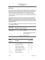
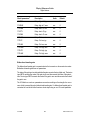
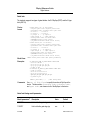
Notation
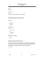
Examples
Description
monospace font
mydiodes.slb
Library files and file names.
key cap or letter
Press J ...
A specific key or key stroke on the
keyboard.
monospace font
Type
Output produced by a printer and
commands/text entered from the
keyboard.
VAC...
Command syntax formats
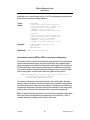
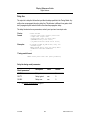
The following table provides the command syntax formats.
Notation
Examples
Description
monospace font abcd
User input including keypad symbols, numerals, and
alphabetic characters as shown; alphabetic
characters are not case sensitive.
< >
<model name>
A required item in a command line. For example,
<model name> in a command line means that the
model name parameter is required.
< >*
<value>*
The asterisk indicates that the item shown in italics
must occur one or more times in the command line.
[ ]
[AC]
Optional item.
[ ]*
[value]*
The asterisk indicates that there is zero or more
occurrences of the specified subject.
< | >
<YES | NO>
Specify one of the given choices.
[ | ]
[ON | OFF]
Specify zero or one of the given choices.
June 2004
10
Product Version 10.2
PSpice Reference Guide
Before you begin
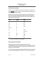
Numeric value conventions
The numeric value and expression conventions in the following table not only apply to the
PSpice Commands on page 23, but also to the device declarations and interactive numeric
entries described in subsequent chapters.
Literal numeric values are written in standard floating point notation. PSpice applies the
default units for the numbers describing the component values and electrical quantities.
However, these values can be scaled by following the number using the appropriate scale
suffix as shown in the following table.
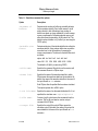
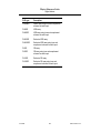
Scale
Symbol
Name
10-15
F
femto-
10-12
P
pico-
10-9
N
nano-
10-6
U
micro-
25.4*10-6
MIL
--
10-3
M
milli-
C
clock cycle1
10+3
K
kilo-
10+6
MEG
mega-
10+9
G
giga-
10+12
T
tera-
1. Clock cycle varies and must be set where applicable.
Numeric expression conventions
Numeric values can also be indirectly represented by parameters; see the
“.PARAM (parameter)” on page 71 command. Numeric values and parameters can be used
together to form arithmetic expressions. PSpice expressions can incorporate the intrinsic
functions shown in the following table.
The Function column lists expressions that PSpice and PSpice A/D recognize. The Meaning
column lists the mathematical definition of the function. There are also some differences
June 2004
11
Product Version 10.2
PSpice Reference Guide
Before you begin
between the intrinsic functions available for simulation and those available for waveform
analysis. Refer to your PSpice User’s Guide for more information about waveform analysis.
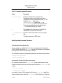
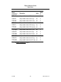
Function1
Meaning
ABS(x)
|x|
ACOS(x)
arccosine of x
-1.0 <= x <= +1.0
ARCTAN(x)
tan-1(x)
result in radians
ASIN(x)
arcsine of x
-1.0 <= x <= +1.0
ATAN(x)
tan-1(x)
result in radians
ATAN2(y,x)
arctan of (y/x)
result in radians
COS(x)
cos(x)
x in radians
COSH(x)
hyperbolic cosine
of x
x in radians
DDT(x)
time derivative of
x
EXP(x)
ex
IF(t, x, y)
x if t=TRUE
y if t=FALSE
Comments
transient analysis only
t is a Boolean expression that evaluates to
TRUE or FALSE and can include logical and
relational operators (see Command line
options on page 15). X and Y are either
numeric values or expressions.
For example,
{IF ( v(1)<THL, v(1), v(1)*v(1)/THL )}
Care should be taken in modeling the
discontinuity between the IF and ELSE parts,
or convergence problems can result.
IMG(x)
imaginary part of x
returns 0.0 for real numbers
result is min if x < min, max if x > max, and x
otherwise
LIMIT(x,min,max
)
LOG(x)
ln(x)
log base e
LOG10(x)
log(x)
log base 10
M(x)
magnitude of x
this produces the same result as ABS(x)
MAX(x,y)
maximum of x and y
June 2004
12
Product Version 10.2
PSpice Reference Guide
Before you begin
Function1
Meaning
MIN(x,y)
minimum of x and y
P(x)
phase of x
returns 0.0 for real numbers
PWR(x,y)
|x|y
the binary operator ** is interchangeable with
PWR(x,y).
or, {x**y}
PWRS(x,y)
Comments
+|x|y (if x>0),
-|x|y (if x<0)
R(x)
real part of x
SCHEDULE
(x1,y1,x2,y
2,... xn,yn)
piecewise constant Must include an entry for TIME=0.
function: from time
All y values must be legal for the associated
x forward use y
parameter.
Time (x) values must be >= 0.
SDT(x)
time integral of x
SGN(x)
signum function
SIN(x)
sin(x)
SINH(x)
hyperbolic sine of x x in radians
STP(x)
1 if x>0.0
0 if x<0.0
For transient analysis only.
x in radians
The unit step function can be used to suppress
a value until a given amount of time has
passed. For instance,
{v(1)*STP(TIME-10ns)}
gives a value of 0.0 until 10ns has elapsed,
then gives v(1).
SQRT(x)
x1/2
TAN(x)
tan(x)
x in radians
TANH(x)
hyperbolic tangent
of x
x in radians
June 2004
13
Product Version 10.2
PSpice Reference Guide
Before you begin
Function1
Meaning
Result is the y value corresponding to x, when
all of the xn,yn points are plotted and
connected by straight lines. If x is greater than
the max xn, then the value is the yn associated
with the largest xn. If x is less than the smallest
xn, then the value is the yn associated with the
smallest xn.
TABLE
(x,x1,y1,x2
,y2,... xn,yn)
1.
Comments
Most numeric specifications in PSpice allow for arithmetic expressions. Some exceptions do
exist and are summarized in your PSpice User’s Guide. There are also some differences
between the intrinsic functions available for simulation and those available for waveform
analysis. Refer to your PSpice User’s Guide for more information about waveform analysis.
Expressions can contain the standard operators as shown in the following table.
Operators
Meaning
arithmetic
+
addition (or string concatenation)
-
subtraction
*
multiplication
/
division
**
exponentiation
PWR()
PWRS()
logical
~
unary NOT
|
boolean OR
^
boolean XOR
&
boolean AND
relational (within IF( ) functions)
==
equality test
!=
non-equality test
June 2004
14
Product Version 10.2
PSpice Reference Guide
Before you begin
Operators
Meaning
>
greater than test
>=
greater than or equal to test
<
less than test
<=
less than or equal to test
Command line options
Command files
A command file is an ASCII text file which contains a list of commands to be executed. A
command file can be specified in multiple ways:
■
at the command line when starting PSpice, Stimulus Editor, or the Model Editor,
■
by choosing Run Commands from the File menu and entering a command file name (for
PSpice and Stimulus Editor only), or
■
at the PROBECMD or STMEDCMD command line, found in the configuration file
pspice.ini.
The command file is read by the program and all of the commands contained within the file
are performed. When the end of the command file is reached, commands are taken from the
keyboard and the mouse. If no command file is specified, all of the commands are received
from the keyboard and mouse.
The ability to record a set of commands can be useful when using PSpice, the Model Editor,
and Stimulus Editor. This is especially useful in PSpice, if you are repeatedly doing the same
simulation and looking at the same waveform with only slight changes to the circuit before
each run. It can also be used to automatically create hardcopy output at the end of very long
(such as overnight) simulation runs.
Creating and editing command files
You can create your own command file using a text editor (such as Notepad). In PSpice and
Stimulus Editor, you can choose Log Commands from the File menu (see Log files on
page 16 for an example) to record a list of transactions in a log file, then choose Run
Commands from the File menu to run the logged file.
June 2004
15
Product Version 10.2
PSpice Reference Guide
Before you begin
Note: After you activate cursors (from the Tools menu, choose Cursor), any mouse or
keyboard movements that you make for moving the cursor will not be recorded in the
command file.
If you choose to create a command file using a text editor, note that the commands in the
command file are the same as those available from the keyboard with these differences:
■
The name of the command or its first capitalized letter can be used.
■
Any line that begins with an * is a comment.
■
Blank lines are ignored, therefore, they can be added to improve the readability of the
command file.
■
The commands @CR, @UP, @DWN, @LEFT, @RIGHT, and @ESC are used to
represent the <Enter>, <↑>, <↓>, <←>, <→>, and <Esc> keys, respectively.
■
The command PAUSE causes PSpice, the Model Editor, or Stimulus Editor to wait until
any key on the keyboard is pressed. In the case of PSpice, this can be useful to examine
a waveform before the command file draws the next one.
The commands are one to a line in the file, but comment and blank lines can be used to make
the file easier to read.
Assuming that a waveform data file has been created by simulating the circuit example.dsn,
you can manually create a command file (using a text editor) called example.cmd which
contains the commands listed below. This set of commands draws a waveform, allows you to
look at it, and then exits PSpice.
* Display trace v(out2) and wait
Trace Add
v(out2)
Pause
* Exit Probe environment
File Exit
See Simulation command line specification format on page 19 and Specifying simulation
command line options on page 21 for specifying command files on the simulation command
line. See Simulation command line specification format on page 19 and Specifying simulation
command line options on page 21 for details on specifying the /C or -c option for PSpice.
Note: The Search Commands feature is a Cursor option for positioning the cursor at a
particular point. You can learn more about Search Commands by consulting PSpice Help.
Log files
Instead of creating command files by hand, using a text editor, you can generate them
automatically by creating a log file while running PSpice, the Model Editor, or Stimulus Editor.
June 2004
16
Product Version 10.2
PSpice Reference Guide
Before you begin
While executing the particular package, all of the commands given are saved in the log file.
The format of the log file is correct for use as a command file.
To create a file in PSpice or Stimulus Editor, from the File menu, choose Log Commands and
enter a log file name. This turns logging on. Any action taken after starting Log Commands
is logged in the named file and can be run in another session by choosing Run Commands.
You can also create a log file for PSpice, Stimulus Editor, or the Model Editor by using the /l
or -l option at the command line. For example:
PROBE /L EXAMPLE.LOG
Of course, you can use a name for the log file that is more recognizable, such as acplots.cmd
(to PSpice, the Model Editor, and Stimulus Editor, the file name is any valid file name for your
computer).
Note: You can use either (/) or (-) as separators, and file names can be in upper or lower
case.
Editing log files
After PSpice, the Model Editor, or Stimulus Editor is finished, the log file is available for editing
to customize it for use as a command file. You can edit the following items:
■
Add blank lines and comments to improve readability (perhaps a title and short
discussion of what the file does).
■
Add the Pause command for viewing waveforms before proceeding.
■
Remove the Exit command from the end of the file, so that PSpice, the Model Editor, and
Stimulus Editor do not automatically exit when the end of the command file is reached.
You can add or delete other commands from the file or even change the file name to be more
recognizable. It is possible to build onto log files, either by using your text editor to combine
files or by running PSpice, the Model Editor, and Stimulus Editor with both a command and
log file:
PROBE /C IN.CMD /L OUT.LOG
The file in.cmd gives the command to PSpice, and PSpice saves the (same) commands into
the out.log file. When in.cmd runs out of commands, and PSpice is taking commands from
the keyboard, these commands also go into the out.log file.
June 2004
17
Product Version 10.2
PSpice Reference Guide
Before you begin
To log commands in PSpice
Use command logging in PSpice to record and save frequently used actions to a command
file. Command files are useful when you need to remember the steps taken in order to display
a set of waveforms for any given data file.
1. From the File menu, choose Log Commands.
2. In the Log File Name text box, type 2traces, then click OK.
A check mark appears next to Log Command to indicate that logging is turned on.
3. From the File menu, choose Open.
4. Select example.dat (located in the examples directory), then click OK.
5. From the Trace menu, choose Add.
6. Select V(OUT1) and V(OUT2), then click OK.
7. From the File menu, choose Log Commands to turn command logging off.
The check mark next to the command disappears. Subsequent actions performed are
not logged in the command file.
You can view the command file using an ASCII text editor, such as Notepad. Command files
can be edited or appended, depending on the types of commands you want to store for future
use. The file 2traces.cmd should look as shown below (with the exception of a different file
path).
*Command file created by Probe - Wed Apr 17 10:33:55
File Open
/Cadence/probe/example.dat
OK
Trace Add
V(OUT1) V(OUT2)
OK
To run the command log
1. From the File menu, choose Run Command.
2. Select 2traces.cmd, then click OK.
The two traces appear.
June 2004
18
Product Version 10.2
PSpice Reference Guide
Before you begin
Simulation command line specification format
The format for specifying command line options for PSpice and PSpice A/D are as follows.
pspice [options] [input file(s)]
Where:
options
One or more of the options listed in Simulation command line options on
page 19. Options can be entered using the dash (-) or slash (/) separator.
input file
Specifies the name of a circuit file for PSpice or PSpice A/D to simulate after it
starts. The input file can be a simulation file (.sim, .cir, .net), data files
(.dat), output files (.out), or any files (*.*). PSpice opens any files whose
extension PSpice does not recognize as a text file.
You can specify multiple input files, but if the output file or data file options are
specified, they apply only to the first specified input file.
The input file name can include wildcard characters (* and ?), in which case all
file names matching the specification are simulated.
Table 1-1 Simulation command line options
Option
Description
-bf<flush
interval>
Determines how often (in minutes) the simulator will flush
the buffers of the waveform data file to disk. This is useful
when a long simulation is left running and the machine
crashes or is restarted. In this case, the data file will be
readable up to the last flush. The default is to flush every
10 minutes. The <flush interval> can be set between 0
and 1440 minutes. A value of zero means not to write
unless necessary.
June 2004
19
Product Version 10.2
PSpice Reference Guide
Before you begin
Table 1-1 Simulation command line options
Option
Description
-bn<number of
buffers>
Determines the number of buffers to potentially allocate
for the waveform data file. Zero buffers means to do all
writing directly to disk. Allocating a large number of
buffers can speed up a large simulation, but will increase
memory requirements. Exceeding physical memory will
either slow down the simulation, or will make it fail. The
default number of buffers is 4 (1 buffer if you are using the
CSDF option).
-bs<buffer size
factor>
Determines the size of the individual buffers for writing the
waveform data file. Using a larger buffer size can reduce
execution time, but at the expense of increasing the
memory requirements. The values for the buffer files work
as follows:
option:-bs0 -bs1 -bs2 -bs3 -bs4 -bs5 -bs6
value: 256 512 1024 2048 4096 8192 16384
The default is 4K (8K if you are using CSDF).
-c<file name>
Specifies the command file, which runs the session until
the command file ends or PSpice stops.
-d <data file>
Specifies the name of the waveform data file to which
PSpice saves the waveform data from the simulation. By
default, the name of the waveform data file is the name of
the input file with a .dat extension.
-e
Exits PSpice after all specified files have been simulated.
This option replaces the -wONLY option.
-i <ini file name>
Specifies the name of an alternate initialization file. If not
specified, the simulator uses: \PSpice\PSpice.ini
-l <file name>
Creates a log file, which saves the commands from this
session. This log file can later be used as an input
command file for PSpice.
-o <output file>
Specifies the output file to which PSpice saves the
simulation output. By default, the name of the output file
name defaults to the name of the input file with an .out
extension.
June 2004
20
Product Version 10.2
PSpice Reference Guide
Before you begin
Table 1-1 Simulation command line options
Option
Description
-p <file name>
Specifies a file that contains goal functions for
Performance Analysis, macro definitions, and display
configurations. This file is loaded after the global .prb file
(specified in the .ini file by the line
PRBFILE=pspice.prb), and the local .prb file
(<file name>.prb), have been loaded. Definitions in
this file will replace definitions from the global or local
.prb files that have already been loaded.
-r
Runs simulation files. If this option is not specified, the
specified files are opened but not simulated.
-t <temp directory
name>
Specifies a directory where PSpice can write temporary
files.
This option replaces the -wTEMP option.
Specifying simulation command line options
Using the pspice.ini configuration file
You can customize your initialization file to include command line options by editing the
PSPICECMDLINE line in the file pspice.ini, using any ASCII text editor, such as Notepad.
These options take effect the next time PSpice A/D starts.
The command line options can be separated by spaces or in a continuous string, therefore:
-c makeplot.cmd -p newamp.prb
-cmakeplot.cmd-pnewamp.prb
are equivalent. The order of the options does not matter.
The command line options that use <file name> assume default extensions. These
command line options can be used without specifying the extension to <file name>. For
example:
-c makeplot -p
newamp
-c makeplot.cmd -p newamp.prb
are equivalent. However, PSpice searches first for the exact <file name> specified for
these command line options, and if that <file name> exists, PSpice uses it. If the exact
June 2004
21
Product Version 10.2
PSpice Reference Guide
Before you begin
<file name> does not exist, PSpice adds default extensions to <file name> and
searches for those. The following default extensions are used:
<file name[.dat]>
waveform data file
-c<file name[.cmd]>
command file
-l<file name[.log]>
log file
-p<file name[.prb]>
displays, goal functions, and macros file
Note: You can learn more about PSpice macros by consulting PSpice Help.
June 2004
22
Product Version 10.2
PSpice Reference Guide
1
Commands
In this Chapter
Standard analyses
.AC (AC analysis) on page 28
.DC (DC analysis) on page 31
.FOUR (Fourier analysis) on page 40
.NOISE (noise analysis) on page 60
.OP (bias point) on page 62
.SENS (sensitivity analysis) on page 88
.TF (transfer) on page 102
.TRAN (transient analysis) on page 103
Output control
.PLOT (plot) on page 73
.PRINT (print) on page 75
.PROBE (Probe) on page 76
.VECTOR (digital output) on page 106
.WATCH (watch analysis results) on
page 108
Simple multi-run analyses
.STEP (parametric analysis) on page 89
.TEMP (temperature) on page 99
Circuit file processing
.END (end of circuit) on page 37
.FUNC (function) on page 41
.INC (include file) on page 43
.LIB (library file) on page 44
.PARAM (parameter) on page 71
Statistical analyses
.MC (Monte Carlo analysis) on page 47
.WCASE (sensitivity/worst-case analysis)
on page 110
Device modeling
.SUBCKT (subcircuit) on page 95
.ENDS (end subcircuit) on page 38
.DISTRIBUTION (userdefined distribution) on page 35
June 2004
.MODEL (model definition) on page 51
.SUBCKT (subcircuit) on page 95
23
Product Version 10.2
PSpice Reference Guide
Commands
Initial conditions
.IC (initial bias point condition) on
page 42
.LOADBIAS (load bias point file) on
page 46
.NODESET (set approximate node
voltage for bias point) on page 59
.SAVEBIAS (save bias point to file) on
page 84
Miscellaneous
.ALIASES, .ENDALIASES (aliases and
endaliases) on page 30
.EXTERNAL (external port) on page 39
.OPTIONS (analysis options) on page 63
.STIMLIB (stimulus library file) on
page 93
June 2004
.STIMULUS (stimulus) on page 94
.TEXT (text parameter) on page 100
* (comment) on page 114
; (in-line comment) on page 115
+ (line continuation) on page 116
24
Product Version 10.2
PSpice Reference Guide
Commands
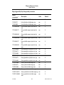
Command reference for PSpice and PSpice A/D
Schematics users enter analysis specifications through the Analysis Setup dialog box (from
the Analysis menu, select Setup).
Function
PSpice command
Description
Standard
Analyses
.AC (AC analysis)
frequency response
.DC (DC analysis)
DC sweep
.FOUR (Fourier analysis)
Fourier components
.NOISE (noise analysis)
noise
.OP (bias point)
bias point
.SENS (sensitivity analysis)
DC sensitivity
.TF (transfer)
small-signal DC transfer function
.TRAN (transient analysis)
transient
Simple MultiRun Analyses
.STEP (parametric analysis)
parametric
.TEMP (temperature)
temperature
Statistical
Analyses
.MC (Monte Carlo analysis)
Monte Carlo
.WCASE (sensitivity/worst-case
analysis)
sensitivity/worst-case
Initial Conditions .IC (initial bias point condition)
.LOADBIAS (load bias point file)
.NODESET (set approximate node
voltage for bias point)
.SAVEBIAS (save bias point to file)
clamp node voltage for bias point
calculation
to restore a .NODESET bias
point
to suggest a node voltage for
bias calculation
to store .NODESET bias point
information
end of subcircuit definition
Device Modeling .ENDS (end subcircuit)
.DISTRIBUTION (userdefined distribution)
.MODEL (model definition)
model parameter tolerance
distribution
modeled device definition
.SUBCKT (subcircuit)
to start subcircuit definition
June 2004
25
Product Version 10.2
PSpice Reference Guide
Commands
Function
PSpice command
Description
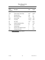
Output Control
.PLOT (plot)
to send an analysis plot to output
file (line printer format)
.PRINT (print)
to send an analysis table to
output file
.PROBE (Probe)
to send simulation results to
Probe data file
.VECTOR (digital output)
digital state output
.WATCH (watch analysis results)
view numerical simulation results
in progress
.END (end of circuit)
end of circuit simulation
description
.FUNC (function)
expression function definition
.INC (include file)
include specified file
.LIB (library file)
reference specified library
.PARAM (parameter)
parameter definition
Circuit File
Processing
June 2004
26
Product Version 10.2
PSpice Reference Guide
Commands
Function
PSpice command
Description
miscellaneous
.ALIASES, .ENDALIASES (aliases
and endaliases) on page 30
to begin and end an alias
definition
.EXTERNAL (external port) on
page 39
to identify nets representing the
outermost (or peripheral)
connections to the circuit being
simulated
.OPTIONS (analysis options) on
page 63
.STIMLIB (stimulus library file) on
page 93
.STIMULUS (stimulus) on page 94
.TEXT (text parameter) on page 100
to set miscellaneous simulation
limits, analysis control
parameters, and output
characters
to specify a stimulus library
name containing .STIMULUS
information
stimulus device definition
text expression, parameter, or
file name used by digital devices
to create a comment line
to add an in-line comment
to continue the text of the
previous line
* (comment) on page 114
; (in-line comment) on page 115
+ (line continuation) on page 116
June 2004
27
Product Version 10.2
PSpice Reference Guide
Commands
.AC (AC analysis)
Purpose
The .AC command calculates the frequency response of a circuit over
a range of frequencies.
General form
.AC <sweep type> <points value>
+ <start frequency value> <end frequency value>
Examples
.AC LIN 101 100Hz 200Hz
.AC OCT 10 1kHz 16kHz
.AC DEC 20 1MEG 100MEG
Arguments and options
<sweep type>
Must be LIN, OCT, or DEC, as described below.
Parameter
Description
Description
LIN
linear sweep
The frequency is swept linearly from the starting to
the ending frequency. The <points value> is
the total number of points in the sweep.
OCT
sweep by
octaves
The frequency is swept logarithmically by octaves.
The <points value> is the number of points per
octave.
DEC
sweep by
decades
The frequency is swept logarithmically by decades.
The <points value> is the number of points per
decade.
<points value>
Specifies the number of points in the sweep, using an integer.
<start frequency value> <end frequency value>
The end frequency value must not be less than the start frequency
value, and both must be greater than zero. The whole sweep must
include at least one point. If a group delay (G suffix) is specified as an
output, the frequency steps must be close enough together that the
phase of that output changes smoothly from one frequency to the
next. Calculate group delay by subtracting the phases of successive
outputs and dividing by the frequency increment.
June 2004
28
Product Version 10.2
PSpice Reference Guide
Commands
Comments
A .PRINT (print) on page 75, .PLOT (plot) on page 73, or
.PROBE (Probe) on page 76 command must be used to get the
results of the AC sweep analysis.
AC analysis is a linear analysis. The simulator calculates the
frequency response by linearizing the circuit around the bias point.
All independent voltage and current sources that have AC values are
inputs to the circuit. During AC analysis, the only independent
sources that have nonzero amplitudes are those using AC
specifications. The SIN specification does not count, as it is used only
during transient analysis.
To analyze nonlinear functions such as mixers, frequency doublers,
and AGC, use .TRAN (transient analysis).
June 2004
29
Product Version 10.2
PSpice Reference Guide
Commands
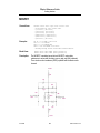
.ALIASES, .ENDALIASES
(aliases and endaliases)
Purpose
The Alias commands set up equivalences between node names and
pin names, so that traces in the Probe display can be identified by
naming a device and pin instead of a node. They are also used to
associate a net name with a node name.
General form
.ALIASES
<device name>
_
.ENDALIASES
Examples
.ALIASES
R_RBIAS
RBIAS (1=$N_0001
2=VDD)
Q_Q3
Q3 (c=$N_0001
b=$N_0001
_
_ (OUT=$N_0007)
.ENDALIASES
<device alias> (<<pin>=<node>>)
_ (<<net>=<node>>)
e=VEE)
The first alias definition shown in the example allows the name RBIAS
to be used as an alias for R_RBIAS, and it relates pin 1 of device
R_RBIAS to node $N_0001 and pin 2 to VDD.
The last alias definition equates net name OUT to node name
$N_0007.
June 2004
30
Product Version 10.2
PSpice Reference Guide
Commands
.DC (DC analysis)
Purpose
The .DC command performs a linear, logarithmic, or nested
DC sweep analysis on the circuit. The DC sweep analysis
calculates the circuit’s bias point over a range of values for
<sweep variable name>.
Sweep type
The sweep can be linear, logarithmic, or a list of values.
Parameter
Description
Meaning
LIN
linear sweep
The sweep variable is swept linearly from the
starting to the ending value.
OCT
sweep by
octaves
Sweep by octaves. The sweep variable is swept
logarithmically by octaves.
DEC
sweep by
decades
Sweep by decades. The sweep variable is swept
logarithmically by decades.
LIST
List of values
Use a list of values.
Linear sweep
General form
.DC [LIN] <sweep variable name>
+ <start value> <end value> <increment value>
+ [nested sweep specification]
Examples
.DC
.DC
.DC
.DC
VIN
LIN
VCE
RES
-.25 .25 .05
I2 5mA -2mA 0.1mA
0V 10V .5V IB 0mA 1mA 50uA
RMOD(R) 0.9 1.1 .001
Arguments and options
<start value>
Can be greater or less than <end value>: that is, the sweep can go
in either direction.
<increment value>
The step size. This value must be greater than zero.
June 2004
31
Product Version 10.2
PSpice Reference Guide
Commands
Comments
The sweep variable is swept linearly from the starting to the ending
value.
The keyword LIN is optional.
Logarithmic sweep
General form
.DC <logarithmic sweep type> <sweep variable name>
+ <start value> <end value> <points value>
+ [nested sweep specification]
Examples
.DC DEC NPN QFAST(IS) 1E-18 1E-14
5
Arguments and options
<logarithmic sweep type>
Must be specified as either DEC (to sweep by decades) or OCT (to sweep
by octaves).
<start value>
Must be positive and less than <end value>.
<points value>
The number of steps per octave or per decade in the sweep. This value
must be an integer.
Comments
June 2004
Either OCT or DEC must be specified for the <logarithmic sweep
type>.
32
Product Version 10.2
PSpice Reference Guide
Commands
Nested sweep
General form
.DC <sweep variable name> LIST <value>*
+[nested sweep specification]
Examples
.DC TEMP LIST 0 20 27 50 80 100 PARAM Vsupply 7.5 15 .5
Arguments and options
<sweep variable name>
After the DC sweep is finished, the value associated with
<sweep variable name> is set back to the value it had before the
sweep started. The following items can be used as sweep variables in a
DC sweep:
Parameter
Description
Source
A name of an independent During the sweep, the source’s voltage
voltage or current source. or current is set to the sweep value.
Model
Parameter
A model type and model
name followed by a model
parameter name in
parenthesis.
Temperature
Use the keyword TEMP for Set the temperature to the sweep value.
<sweep variable na For each value in the sweep, all the
me>.
circuit components have their model
parameters updated to that temperature.
Global
Parameter
Use the keyword PARAM, During the sweep, the global parameter’s
followed by the parameter value is set to the sweep value and all
name, for
expressions are reevaluated.
<sweep variable na
me>.
June 2004
Meaning
33
The parameter in the model is set to the
sweep value. The following model
parameters cannot be (usefully) swept: L
and W for the MOSFET device (use LD
and WD as a work around), and any
temperature parameters, such as TC1
and TC2 for the resistor.
Product Version 10.2
PSpice Reference Guide
Commands
Comments
For a nested sweep, a second sweep variable, sweep type, start, end,
and increment values can be placed after the first sweep. In the nested
sweep example, the first sweep is the inner loop: the entire first sweep is
performed for each value of the second sweep.
When using a list of values, there are no start and end values. Instead,
the numbers that follow the keyword LIST are the values that the sweep
variable is set to.
The rules for the values in the second sweep are the same as for the first.
The second sweep generates an entire .PRINT (print) on page 75 table
or .PLOT (plot) on page 73 plot for each value of the sweep. Probe
displays nested sweeps as a family of curves.
June 2004
34
Product Version 10.2
PSpice Reference Guide
Commands
.DISTRIBUTION (user-defined distribution)
Purpose
The .DISTRIBUTION command defines a user distribution for
tolerances, and is only used with Monte Carlo and sensitivity/worst-case
analyses. The curve described by a .DISTRIBUTION command controls
the relative probability distribution of random numbers generated by
PSpice to calculate model parameter deviations.
General form
DISTRIBUTION <name> (<deviation> <probability>)*
Examples
.DISTRIBUTION bi_modal (-1,1) (-.5,1) (-.5,0) (.5,0)
+ (.5,1) (1,1)
.DISTRIBUTION triangular (-1,0) (0,1) (1,0)
Arguments and options
(<deviation> <probability>)
Defines the distribution curve by pairs, or corner points, in a piecewise
linear fashion. You can specify up to 100 value pairs.
<deviation>
Must be in the range (-1,+1), which matches the range of the random
number generator. No <deviation> can be less than the previous
<deviation> in the list, although it can repeat the previous value.
<probability>
Represents a relative probability, and must be positive or zero.
Comments
When using Schematics, several distributions can be defined by
configuring an include file containing the .DISTRIBUTION command. For
details on how to do this, refer to your PSpice User’s Guide.
If you are not using Schematics, a user-defined distribution can be
specified as the default by setting the DISTRIBUTION parameter in the
.OPTIONS (analysis options) command.
June 2004
35
Product Version 10.2
PSpice Reference Guide
Commands
Deriving updated parameter values
The updated value of a parameter is derived from a combination of a random number, the
distribution, and the tolerance specified. This method permits distributions which have
different excursions in the positive and negative directions. It also allows the use of one
distribution even if the tolerances of the components are different so long as the general
shape of the distributions are the same.
1. Generate a <temporary random number> in the range (0, 1).
2. Normalize the area under the specified distribution.
3. Set the <final random number> to the point where the area under the normalized
distribution equals the <temporary random number>.
4. Multiply this <final random number> by the specified tolerance.
Usage example
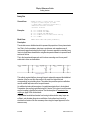
To illustrate, assume there is a 1.0 µfd capacitor that has a variation of -50% to +25%, and
another that has tolerances of -10% to +5%. Note that both capacitors’ tolerances are in the
same general shape, i.e., both have negative excursions twice as large as their positive
excursions.
.distribution cdistrib (-1,1) (.5, 1) (.5, 0) (1, 0)
c1 1 0 cmod 11u
c2 1 0 cmod2 1u
.model cmod1 cap (c=1 dev/cdistrib 50%)
.model cmod2 cap (c=1 dev/cdistrib 10%)
The steps taken for this example are as follows:
1. Generate a <temporary random value> of 0.3.
2. Normalize the area under the cdistrib distribution (1.5) to 1.0.
3. The <final random number> is therefore -0.55 (the point where the normalized area
equals 0.3).
4. For c1, this -0.55 is then scaled by 50%, resulting in -0.275; for c2, it is scaled by 10%,
resulting in -0.055.
Note: Separate random numbers are generated for each parameter that has a tolerance
unless a tracking number is specified.
June 2004
36
Product Version 10.2
PSpice Reference Guide
Commands
.END (end of circuit)
Purpose
The .END command marks the end of the circuit. All the data and every
other command must come before it. When the .END command is
reached, PSpice does all the specified analyses on the circuit.
General form
.END
Examples
* 1st circuit in file
... circuit definition
.END
* 2nd circuit in file
... circuit definition
.END
Comments
There can be more than one circuit in an input file. Each circuit is marked
by an .END command. PSpice processes all the analyses for each circuit
before going on to the next one.
Everything is reset at the beginning of each circuit. Having several
circuits in one file gives the same results as having them in separate files
and running each one separately. However, all the simulation results go
into one .OUT file and one .DAT file. This is a convenient way to arrange
a set of runs for overnight operation.
Note: The last statement in an input file must be an .END command.
June 2004
37
Product Version 10.2
PSpice Reference Guide
Commands
.ENDS (end subcircuit)
Purpose
The .ENDS command marks the end of a subcircuit definition (started by
a .SUBCKT (subcircuit) statement.
General form
.ENDS [subcircuit name]
Examples
.ENDS
.ENDS circuit_name
Comments
It is a good practice to repeat the subcircuit name though this is not
required.
For a detailed explanation see .SUBCKT (subcircuit) on page 95.
June 2004
38
Product Version 10.2
PSpice Reference Guide
Commands
.EXTERNAL (external port)
Purpose
External ports are provided as a means of identifying and
distinguishing those nets representing the outermost (or peripheral),
connections to the circuit being simulated. The external port statement
.EXTERNAL applies only to nodes that have digital devices attached to
them.
General form
.EXTERNAL <attribute> <node-name>*
Examples
.EXTERNAL
.EXTERNAL
.EXTERNAL
INPUT Data1, Data2, Data3
OUTPUT P1
BIDIRECTIONAL BPort1 BPort2 BPort3
Arguments and options
<attribute>
One of the keywords INPUT, OUTPUT, or BIDIRECTIONAL, describing
the usage of the port.
<node_name>
One or more valid PSpice A/D node names.
Comments
When a node is included in a .EXTERNAL statement it is identified as
a primary observation point. For example, if you are modeling and
simulating a PCB-level description, you could place an .EXTERNAL (or
its Capture symbol counterparts) on the edge pin nets to describe the
pin as the external interface point of the network.
PSpice recognizes the nets marked as .EXTERNAL when reporting
any sort of timing violation. When a timing violation occurs, PSpice
analyzes the conditions that would permit the effects of such a
condition to propagate through the circuit. If, during this analysis, a net
marked external is encountered, PSpice reports the condition as a
Persistent Hazard, signifying that it has a potential effect on the
externally visible behavior of the circuit. For more information on
Persistent Hazards, refer to your PSpice User’s Guide.
Port specifications are inserted in the netlist by Capture whenever an
external port symbol, EXTERNAL_IN, EXTERNAL_OUT, or
EXTERNAL_BI is used. Refer to your PSpice User’s Guide for more
information.
June 2004
39
Product Version 10.2
PSpice Reference Guide
Commands
.FOUR (Fourier analysis)
Purpose
Fourier analysis decomposes the results of a transient analysis into
Fourier components.
General form
.FOUR <frequency value> [no. harmonics value] <output
variable>
Examples
.FOUR 10kHz V(5) V(6,7) I(VSENS3)
.FOUR 60Hz 20 V(17)
.FOUR 10kHz V([OUT1],[OUT2])
Arguments and options
<output variable>
An output variable of the same form as in a .PRINT (print) command or
.PLOT (plot) command for a transient analysis.
<frequency value>
The fundamental frequency. Not all of the transient results are used, only
the interval from the end, back to 1/<frequency value> before the
end is used. This means that the transient analysis must be at least 1/
<frequency value> seconds long.
Comments
The analysis results are obtained by performing a Fourier integral on the
results from a transient analysis. The analysis must be supplied with
specified output variables using evenly spaced time points. The time
interval used is <print step value> in the .TRAN (transient analysis)
command, or 1% of the <final time value> (TSTOP) if smaller, and a
2nd-order polynomial interpolation is used to calculate the output value
used in the integration. The DC component, the fundamental, and the 2nd
through 9th harmonics of the selected voltages and currents are
calculated by default, although more harmonics can be specified.
A .FOUR command requires a .TRAN command, but Fourier analysis
does not require .PRINT, .PLOT, or .PROBE (Probe) commands. The
tabulated results are written to the output file (.out) as the transient
analysis is completed.
Note: The results of the .FOUR command are only available in the
output file. They cannot be viewed in Probe.
June 2004
40
Product Version 10.2
PSpice Reference Guide
Commands
.FUNC (function)
Purpose
The .FUNC command defines functions used in expressions.
Besides their obvious flexibility, they are useful for where there are
several similar sub expressions in a circuit file.
General
form
.FUNC <name> ([arg]*) {<body>}
Examples
.FUNC
.FUNC
.FUNC
.FUNC
E(x) {exp(x)}
DECAY(CNST) {E(-CNST*TIME)}
TRIWAV(x) {ACOS(COS(x))/3.14159}
MIN3(A,B,C) {MIN(A,MIN(B,C))}
Arguments and options
.FUNC
Does not have to precede the first use of the function name.
Functions cannot be redefined and the function name must not be
the same as any of the predefined functions (e.g., SIN and
SQRT). See Numeric expression conventions on page 11 for a list
of valid expressions. .FUNC arguments cannot be node names.
<body>
Refers to other (previously defined) functions; the second
example, DECAY, uses the first example, E.
[arg]
Specifies up to 10 arguments in a definition. The number of
arguments in the use of a function must agree with the number in
the definition. Functions can be defined as having no arguments,
but the parentheses are still required. Parameters, TIME, other
functions, and the Laplace variable s are allowed in the body of
function definitions.
Comments
The <body> of a defined function is handled in the same way as
any math expression; it is enclosed in curly braces {}. Previous
versions of PSpice did not require this, so for compatibility the
<body> can be read without braces, but a warning is generated.
Note: Creating a file of frequently used .FUNC definitions and
accessing them using an .INC command near the beginning of
the circuit file can be helpful. .FUNC commands can also be
defined in subcircuits. In those cases they only have local scope.
June 2004
41
Product Version 10.2
PSpice Reference Guide
Commands
.IC (initial bias point condition)
Purpose
The .IC command sets initial conditions for both small-signal and
transient bias points. Initial conditions can be given for some or all of the
circuit’s nodes.
.IC sets the initial conditions for the bias point only. It does not affect a
.DC (DC analysis) sweep.
General form
.IC < V(<node> [,<node>])=<value> >*
.IC <I(<inductor>)=<value>>*
Examples
.IC V(2)=3.4 V(102)=0 V(3)=-1V I(L1)=2uAmp
.IC V(InPlus,InMinus)=1e-3 V(100,133)=5.0V
Arguments and options
<value>
A voltage assigned to <node> (or a current assigned to an inductor) for
the duration of the bias point calculation.
Comments
The voltage between two nodes and the current through an inductor can
be specified. During bias calculations, PSpice clamps the voltages to
specified values by attaching a voltage source with a 0.0002 ohm series
resistor between the specified nodes. After the bias point has been
calculated and the transient analysis started, the node is released.
If the circuit contains both the .IC command and
.NODESET (set approximate node voltage for bias point) command for
the same node or inductor, the .NODESET command is ignored (.IC
overrides .NODESET).
Refer to your PSpice User’s Guide for more information on setting
initial conditions.
Note: An .IC command that imposes nonzero voltages on inductors
cannot work properly, since inductors are assumed to be short circuits for
bias point calculations. However, inductor currents can be initialized.
June 2004
42
Product Version 10.2
PSpice Reference Guide
Commands
.INC (include file)
Purpose
The .INC command inserts the contents of another file.
General form
.INC <file name>
Examples
.INC "SETUP.CIR"
.INC "C:\LIB\VCO.CIR"
Arguments and options
<file name>
Any character string that is a valid file name for your computer system.
Comments
Including a file is the same as bringing the file’s text into the circuit file.
Everything in the included file is actually read in. The comments of the
included file are then treated just as if they were found in the parent file.
Included files can contain any valid PSpice statements, with the following
conditions:
■
The included files should not contain title lines unless they are
commented.
■
Included files can be nested up to 4 levels.
Note: Every model and subcircuit definition, even if not needed, takes up
memory.
June 2004
43
Product Version 10.2
PSpice Reference Guide
Commands
.LIB (library file)
Purpose
The .LIB command references a model or subcircuit library in another
file.
General form
.LIB [file_name]
Examples
.LIB
.LIB linear.lib
.LIB "C:\lib\bipolar.lib"
Arguments and options
[file_name]
Any character string that is a valid file name for the computer system.
Comments
Library files can contain any combination of the following:
■
comments
■
.MODEL (model definition) commands
■
subcircuit definitions (including the .SUBCKT (subcircuit) command)
■
.PARAM (parameter) commands
■
.FUNC (function) commands
■
.LIB commands
No other statements are allowed. For further discussion of library files,
refer to your PSpice User’s Guide.
If [file_name] is left off, all references point to the master library file,
nom.lib. When a library file is referenced in Schematics, PSpice first
searches for the file in the current working directory, then searches in the
directory specified by the LIBPATH variable (set in PSpice.ini).
When any library is modified, PSpice creates an index file based on the
first use of the library. The index file is organized so that PSpice can find
a particular .MODEL or .SUBCKT (subcircuit) quickly, despite the size of
the library file.
Note: The index files have to be regenerated each time the library is
changed. Because of this, it is advantageous to configure separately any
frequently changed libraries.
June 2004
44
Product Version 10.2
PSpice Reference Guide
Commands
Nom.lib normally contains references to all parts in the PSpice
Standard Model Library. You can edit nom.lib to include your custom
model references.
June 2004
45
Product Version 10.2
PSpice Reference Guide
Commands
.LOADBIAS (load bias point file)
Purpose
The .LOADBIAS command loads the contents of a bias point file. It is
helpful in setting initial bias conditions for subsequent simulations.
However, the use of .LOADBIAS does not guarantee convergence.
General form
.LOADBIAS <file name>
Examples
.LOADBIAS "SAVETRAN.NOD"
.LOADBIAS "C:\PROJECT\INIT.FIL"
Arguments and options
<file name>
Any character string which is a valid computer system file name, but it
must be enclosed in quotation marks.
Comments
Normally, the bias point file is produced by a previous circuit simulation
using the .SAVEBIAS (save bias point to file) command.
The bias point file is a text file that contains one or more comment lines
and a .NODESET (set approximate node voltage for bias point)
command setting the bias point voltage or inductor current values. If a
fixed value for a transient analysis bias point needs to be set, this file can
be edited to replace the .NODESET command with an
.IC (initial bias point condition) command.
Note: Any nodes mentioned in the loaded file that are not present in the
circuit are ignored, and a warning message will be generated.
To echo the .LOADBIAS file contents to the output file, use the EXPAND
option on the .OPTIONS (analysis options) command.
June 2004
46
Product Version 10.2
PSpice Reference Guide
Commands
.MC (Monte Carlo analysis)
Purpose
The .MC command causes a Monte Carlo (statistical) analysis of the
circuit and causes PSpice to perform multiple runs of the selected
analysis (DC, AC, or transient).
General form
.MC <#runs value> <analysis> <output variable> <function>
[option]* SEED=value]
Examples
.MC
.MC
.MC
.MC
10
50
20
10
TRAN V(5) YMAX
DC IC(Q7) YMAX LIST
AC VP(13,5) YMAX LIST OUTPUT ALL
TRAN V([OUT1],[OUT2]) YMAX SEED=9321
Arguments and options
<#runs value>
The total number of runs to be performed (for printed results the upper
limit is 2,000, and for results to be viewed in Probe, the limit is 400).
<analysis>
Specifies at least one analysis type: .DC (DC analysis), Table on
page 28, or .TRAN (transient analysis). This analysis is repeated in
subsequent passes. All analyses that the circuit contains are performed
during the nominal pass. Only the selected analysis is performed during
subsequent passes.
<output variable>
Identical in format to that of a .PRINT (print) output variable.
<function>
Specifies the operation to be performed on the values of <output
variable> to reduce these to a single value. This value is the basis
for the comparisons between the nominal and subsequent runs.The
<function> can be any one of the following:
Function
Definition
YMAX
Find the absolute value of the greatest difference in each
waveform from the nominal run.
MAX
Find the maximum value of each waveform.
June 2004
47
Product Version 10.2
PSpice Reference Guide
Commands
Function
Definition
MIN
Find the minimum value of each waveform.
RISE_EDGE(<value>)
Find the first occurrence of the waveform crossing above
the threshold <value>. The waveform must have one or
more points at or below <value> followed by one
above; the output value listed is the first point that the
waveform increases above <value>.
FALL_EDGE(<value>)
Find the first occurrence of the waveform crossing below
the threshold <value>. The waveform must have one or
more points at or above <value> followed by one
below; the output value listed is where the waveform
decreases below <value>.
June 2004
48
Product Version 10.2
PSpice Reference Guide
Commands
Note: <function> and all [option]s (except for <output type>) have no effect on the
Probe data that is saved from the simulation. They are only applicable to the output file.
[option]*
Can include zero or more of the following options:
Option
Definition
LIST
Lists, at the beginning of each
run, the model parameter
values actually used for each
component during that run.
OUTPUT
<output type>
Asks for an output from
subsequent runs, after the
nominal (first) run. The output
from any run is governed by a
.PRINT, .PLOT, and .PROBE
command in the file. If OUTPUT
is omitted, then only the
nominal run produces output.
The <output type> is one
of the ones shown in the
examples to the right.
RANGE1
(<low value>,
<high value>)
Example
Restricts the range over which
<function> is evaluated.
An asterisk (*) can be used in
place of a <value> to show
for all values.
ALL forces all output to be
generated (including the
nominal run).
FIRST <N> generates output
only during the first n runs.
EVERY <N> generates output
every nth run.
RUNS <N>* does analysis
and generates output only for
the listed runs. Up to 25
values can be specified in the
list.
YMAX RANGE(*,.5)
YMAX is evaluated for values
of the sweep variable (e.g.,
time and frequency) of .5 or
less.
MAX RANGE(-1,*)
The maximum of the output
variable is found for values of
the sweep variable of -1 or
more.
1.
June 2004
If RANGE is omitted, then <function> is evaluated over the whole sweep range. This is
equivalent to RANGE(*,*).
49
Product Version 10.2
PSpice Reference Guide
Commands
[SEED=value]
Defines the seed for the random number generator within the Monte
Carlo analysis (The Art of Computer Programming, Donald Knuth,
vol. 2, pg. 171, “subtractive method”).
<value>
Must be an odd integer ranging from 1 to 32,767. If the seed value is not
set, its default value is 17,533.
Note: For almost all analyses, the default seed value is adequate to
achieve a constant set of results. The seed value can be modified within
the integer value as required.
Comments
The first run uses nominal values of all components. Subsequent runs
use variations on model parameters as specified by the DEV and LOT
tolerances on each .MODEL (model definition) parameter.
The other specifications on the .MC command control the output
generated by the Monte Carlo analysis.
For more information on Monte Carlo analysis, refer to your PSpice
User’s Guide.
June 2004
50
Product Version 10.2
PSpice Reference Guide
Commands
.MODEL (model definition)
Purpose
The .MODEL command defines a set of device parameters that can be
referenced by devices in the circuit.
General form
.MODEL <model name> [AKO: <reference model name>]
+ <model type>
+ ([<parameter name> = <value> [tolerance specification]]*
+ [T_MEASURED=<value>] [[T_ABS=<value>] or
+ [T_REL_GLOBAL=<value>] or [T_REL_LOCAL=<value>]])
Examples
.MODEL
.MODEL
.MODEL
.MODEL
.MODEL
.MODEL
.MODEL
.MODEL
RMAX RES (R=1.5 TC1=.0002 TC2=.005)
DNOM D (IS=1E-9)
QDRIV NPN (IS=1E-7 BF=30)
MLOAD NMOS(LEVEL=1 VTO=.7 CJ=.02pF)
CMOD CAP (C=1 DEV 5%)
DLOAD D (IS=1E-9 DEV .5% LOT 10%)
RTRACK RES (R=1 DEV/GAUSS 1% LOT/UNIFORM 5%)
QDR2 AKO:QDRIV NPN (BF=50 IKF=50m)
Arguments and options
<model name>
The model name which is used to reference a particular model.
<reference model name>
The model types of the current model and the AKO (A Kind Of) reference
model must be the same. The value of each parameter of the referenced
model is used unless overridden by the current model, e.g., for QDR2 in
the last example, the value of IS derives from QDRIV, but the values of
BF and IKF come from the current definition. Parameter values or
formulas are transferred, but not the tolerance specification. The
referenced model can be in the main circuit file, accessed through a .INC
command, or it can be in a library file; see .LIB (library file).
<model type>
Must be one of the types outlined in the table that follows.
Devices can only reference models of a corresponding type; for example:
June 2004
■
A JFET can reference a model of types NJF or PJF, but not of type
NPN.
■
There can be more than one model of the same type in a circuit,
although they must have different names.
51
Product Version 10.2
PSpice Reference Guide
Commands
Following the <model type> is a list of parameter values enclosed by
parentheses. None, any, or all of the parameters can be assigned
values. Default values are used for all unassigned parameters. The lists
of parameter names, meanings, and default values are found in the
individual device descriptions.
June 2004
52
Product Version 10.2
PSpice Reference Guide
Commands
Model type
Instance name Type of device
CAP
Cxxx
capacitor
CORE
Kxxx
nonlinear, magnetic core (transformer)
D
Dxxx
diode
DINPUT
Nxxx
digital input device (receive from digital)
DOUTPUT
Oxxx
digital output device (transmit to digital)
GASFET
Bxxx
N-channel GaAs MESFET
IND
Lxxx
inductor
ISWITCH
Wxxx
current-controlled switch
LPNP
Qxxx
lateral PNP bipolar transistor
NIGBT
Zxxx
N-channel insulated gate bipolar transistor (IGBT)
NJF
Jxxx
N-channel junction FET
NMOS
Mxxx
N-channel MOSFET
NPN
Qxxx
NPN bipolar transistor
PJF
Jxxx
P-channel junction FET
PMOS
Mxxx
P-channel MOSFET
PNP
Qxxx
PNP bipolar transistor
RES
Rxxx
resistor
TRN
Txxx
lossy transmission line
UADC
Uxxx
multi-bit analog-to-digital converter
UDAC
Uxxx
multi-bit digital-to-analog converter
UDLY
Uxxx
digital delay line
UEFF
Uxxx
edge-triggered flip-flop
UGATE
Uxxx
standard gate
UGFF
Uxxx
gated flip-flop
UIO
Uxxx
digital I/O model
UTGATE
Uxxx
tristate gate
VSWITCH
Sxxx
voltage-controlled switch
June 2004
53
Product Version 10.2
PSpice Reference Guide
Commands
[tolerance specification]
Appended to each parameter, using the format:
[DEV [track&dist] <value>[%]] [LOT [track&dist] <value>[%]]
to specify an individual device (DEV) and the device lot (LOT)
parameter value deviations. The tolerance specification is used by the
.MC (Monte Carlo analysis) analysis only.
The LOT tolerance requires that all devices that refer to the same model
use the same adjustments to the model parameter. DEV tolerances are
independent, that is each device varies independently. The % shows a
relative (percentage) tolerance. If it is omitted, <value> is in the same
units as the parameter itself.
[track & dist]
Specifies the tracking and non-default distribution, using the format:
[/<lot #>][/<distribution name>]
These specifications must immediately follow the keywords DEV and
LOT (without spaces) and are separated by /.
<lot #>
Specifies which of ten random number generators, numbered 0 through
9, are used to calculate parameter value deviations. This allows
deviations to be correlated between parameters in the same model, as
well as between models. The generators for DEV and LOT tolerances
are distinct: there are ten generators for DEV tracking and ten
generators for LOT tracking. Tolerances without <lot #> are assigned
individually generated random numbers.
<distribution name>
The distribution name is one of the following. The default distribution
can be set by using the DISTRIBUTION parameter of the
.OPTIONS (analysis options) command.
Distribution
name
UNIFORM
June 2004
Function
Generates uniformly distributed deviations over the range
±<value>.
54
Product Version 10.2
PSpice Reference Guide
Commands
Distribution
name
Function
GAUSS
Generates deviations using a Gaussian distribution over the range
±3σ and <value> specifies the ±1σ deviation (i.e., this generates
deviations greater than ±<value>).
<user
name>
Generates deviations using a user-defined distribution and
<value> specifies the ±1 deviation in the user definition; see the
.DISTRIBUTION (user-defined distribution).
Comments
The examples are for the .MODEL parameter. The last example uses the
AKO syntax to reference the parameters of the model QDRIV in the third
example.
For more information, refer to your PSpice User’s Guide.
June 2004
55
Product Version 10.2
PSpice Reference Guide
Commands
Parameters for setting temperature
Some passive and semiconductor devices (C, L, R, B, D, J, M, and Q) have two levels of
temperature attributes that can be customized on a model-by-model basis.
First, the temperature at which the model parameters were measured can be defined by using
one of the following model parameter formats in the .MODEL command line:
T_MEASURED = <literal value>
T_MEASURED = { <parameter> }
This overrides the nominal TNOM value which is set in the .OPTIONS (analysis options)
command line (default = 27°C). All other parameters listed in the .MODEL command are
assumed to have been measured at T_MEASURED.
In addition to the measured model parameter temperature, current device temperatures can
be customized to override the circuit’s global temperature specification defined by the
.TEMP (temperature) command line (or equivalent .STEP TEMP or .DC TEMP). There are
three forms, as described below.
Table 1-1 Model parameters for device temperature
.MODEL
format
Parameter format
Referencing
device
temperature
absolute
temperature
standard
T_ABS=<value >
T_ABS
relative to current
temperature
standard
T_REL_GLOBAL=<value >
global temperature
Description
relative to AKO
AKO
model temperature
+ T_REL_GLOBAL
T_REL_LOCAL=<value >
T_ABS(AKO
Model )
+ T_REL_LOCAL
For all formats, <value> can be a literal value or a parameter of the form
{<parameter name>}. A maximum of one device temperature customization can coexist
using the T_MEASURED customization. For example,
.MODEL
PNP_NEW PNP( T_ABS=35 T_MEASURED=0 BF=90 )
defines a new model PNP_NEW, where BF was measured at 0°C. Any bipolar transistor
referencing this model has an absolute device temperature of 35°C.
June 2004
56
Product Version 10.2
PSpice Reference Guide
Commands
Examples
One
This example demonstrates device temperatures set relative to the global temperature of the
circuit:
.TEMP
.MODEL
10 30 40
PNP_NEW PNP( T_REL_GLOBAL=-5 BF=90 )
This produces three PSpice runs where global temperature changes from 10° to 30° to 40°C,
respectively, and any bipolar transistor that references the PNP_NEW model has a device
temperature of 5°, 25°, or 35°C, respectively.
Two
This example sets the device temperature relative to a referenced AKO model:
.MODEL
.MODEL
PNP_NEW PNP( AKO:PNP_OLD T_REL_LOCAL=10)
PNP_OLD PNP( T_ABS=20)
Any bipolar transistor referencing the PNP_NEW model has a device temperature of 30°C.
Special considerations
There are a few special considerations when using these temperature parameters:
■
If the technique for current device temperature is using the value relative to an AKO
model’s absolute temperature (T_ABS), and the AKO referenced model does not specify
T_ABS, then the T_REL_LOCAL specification is ignored and the standard global
temperature specification is used.
■
These temperature parameters cannot be used with the DEV and LOT model parameter
tolerance feature.
■
A DC sweep analysis can be performed on these parameters so long as the temperature
parameter assignment is to a variable parameter. For example:
.PARAM
.MODEL
.DC PARAM
PTEMP 27
PNP_NEW PNP ( T_ABS={PTEMP} )
PTEMP 27 35 1
This method produces a single DC sweep in PSpice where any bipolar transistor referencing
the PNP_NEW model has a device temperature which is swept from 27˚C to 35˚C in 1˚C
increments.
A similar effect can be obtained by performing a parametric analysis. For instance:
June 2004
57
Product Version 10.2
PSpice Reference Guide
Commands
.PARAM PTEMP 27
.MODEL PNP_NEW PNP( T_ABS={PTEMP} )
.STEP PARAM
PTEMP 27 35 1
This method produces nine PSpice runs where the PNP_NEW model temperature steps from
27°C to 35°C in increments of 1°C, one step per run.
■
The effect of a temperature parameter is evaluated once prior to the bias point
calculation, unless parameters are swept by means of a .DC PARAM or .STEP PARAM
analysis described above. In these cases, the temperature parameter’s effect is
reevaluated once for each value of the swept variable.
June 2004
58
Product Version 10.2
PSpice Reference Guide
Commands
.NODESET (set approximate node voltage for bias point)
Purpose
The .NODESET command helps calculate the bias point by providing an
initial best guess for some node voltages and/or inductor currents. Some
or all of the circuit’s node voltages and inductor currents can be given the
initial guess, and in addition, the voltage between two nodes can be
specified.
General form
.NODESET < V(<node> [,<node>])=<value> >*
.NODESET <I(<inductor>)=<value>>
Examples
.NODESET V(2)=3.4 V(102)=0 V(3)=-1V I(L1)=2uAmp
.NODESET V(InPlus,InMinus)=1e-3 V(100,133)=5.0V
Comments
This command is effective for the bias point (both small-signal and
transient bias points) and for the first step of the DC sweep. It has no
effect during the rest of the DC sweep, nor during a transient analysis.
Unlike the .IC (initial bias point condition) command, .NODESET
provides only an initial guess for some initial values. It does not clamp
those nodes to the specified voltages. However, by providing an initial
guess, .NODESET can be used to break the tie in, for instance, a flip-flop,
and make it come up in a required state.
If both the .IC command and .NODESET command are present, the
.NODESET command is ignored for the bias point calculations (.IC
overrides .NODESET).
Note: For Capture-based designs, refer to your PSpice User’s Guide
for more information on setting initial conditions.
June 2004
59
Product Version 10.2
PSpice Reference Guide
Commands
.NOISE (noise analysis)
Purpose
The .NOISE command performs a noise analysis of the circuit.
General form
.NOISE V(<node> [,<node>]) <name> [interval value]
Examples
.NOISE
.NOISE
.NOISE
.NOISE
.NOISE
V(5)
VIN
V(101) VSRC 20
V(4,5) ISRC
V([OUT1]) V1
V([OUT1],[OUT2]) V1
Note: For the node names starting with alphabets, square brackets
should be used as in the last example.
Arguments and options
V(<node> [,<node>])
Output voltage. It has a form such as V(5), which is the voltage at the
output node five, or a form such as V(4,5), which is the output voltage
between two nodes four and five.
<name>
The name of an independent voltage or current source where the
equivalent input noise is calculated. The <name> is not itself a noise
generator, but only a place where the equivalent input noise is calculated.
[interval value]
Integer that specifies how often the detailed noise analysis data is written
to the output file.
June 2004
60
Product Version 10.2
PSpice Reference Guide
Commands
Comments
A noise analysis is performed in conjunction with an AC sweep analysis
and requires an .AC (AC analysis) command. When .NOISE is used,
noise data is recorded in the Probe .DAT file for each frequency in the
AC sweep.
The simulator computes:
■
Device noise for every resistor and semiconductor in the circuit
(propagated to a specified output node)
■
Total input and output noise
At each frequency, each noise generator’s contribution is calculated and
propagated to the output node. At that point, all the propagated noise
values are RMS-summed to calculate the total output noise. The gain
from the input source to the output voltage, the total output noise, and the
equivalent input noise are all calculated.
For more information, refer to the AC Analyses chapter of your PSpice
User’s Guide.
If:
<name> is a voltage source
then:
the input noise units are volt/hertz1/2
If:
<name> is a current source
then:
the input noise units are amp/hertz1/2
The output noise units are always volt/hertz1/2.
Every nth frequency, where n is the print interval, a detailed table is
printed showing the individual contributions of all the circuit’s noise
generators to the total noise. These values are the noise amounts
propagated to the output node, not the noise amounts at each generator.
If [interval value] is not present, then no detailed table is printed.
The detailed table is printed while the analysis is being performed and
does not need a .PRINT (print) command or a .PLOT (plot) command.
The output noise and equivalent input noise can be printed in the output
by using a .PRINT command or a .PLOT command.
June 2004
61
Product Version 10.2
PSpice Reference Guide
Commands
.OP (bias point)
Purpose
The .OP command causes detailed information about the bias point to be
printed.
General form
.OP
Examples
.OP
Comments
This command does not write output to the Probe data file. The bias point
is calculated regardless of whether there is a .OP command. Without the
.OP command, the only information about the bias point in the output is
a list of the node voltages, voltage source currents, and total power
dissipation.
Using a .OP command can cause the small-signal (linearized)
parameters of all the nonlinear controlled sources and all the
semiconductor devices to be printed in the output file.
The .OP command controls the output for the regular bias point only. The
.TRAN (transient analysis) command controls the output for the transient
analysis bias point.
Note: If no other analysis is performed, then no Probe data file is
created.
June 2004
62
Product Version 10.2
PSpice Reference Guide
Commands
.OPTIONS (analysis options)
Purpose
The .OPTIONS command is used to set all the options, limits, and control
parameters for the simulator.
General form
.OPTIONS [option name]* [ <option name>=<value> ]*
Examples
.OPTIONS NOECHO NOMOD DEFL=12u DEFW=8u DEFAD=150p
+ DEFAS=150p
.OPTIONS ACCT RELTOL=.01
.OPTIONS DISTRIBUTION=GAUSS
.OPTIONS DISTRIBUTION=USERDEF1
Comments
The options can be listed in any order. There are two kinds of options:
those with values, and those without values. Options without values are
flags that are activated by simply listing the option name.
The .OPTIONS command is cumulative. That is, if there are two (or
more) of the .OPTIONS command, the effect is the same as if all the
options were listed together in one .OPTIONS command. If the same
option is listed more than once, only its last value is used.
For SPICE options not available in PSpice, see Differences between
PSpice and Berkeley SPICE2 on page 117.
Flag options
The default for any flag option is off or no (i.e., the opposite of specifying the option). Flag
options affect the output file unless otherwise specified.
Flag option
Meaning
ACCT
Summary and accounting information is printed at the end of all the
analyses (refer to your PSpice User’s Guide for further information
on ACCT).
EXPAND
Lists devices created by subcircuit expansion and lists contents of the
bias point file; see .SAVEBIAS (save bias point to file) and
.LOADBIAS (load bias point file).
LIBRARY
Lists lines used from library files.
LIST
Lists a summary of the circuit elements (devices).
NOBIAS
Suppresses the printing of the bias point node voltages.
June 2004
63
Product Version 10.2
PSpice Reference Guide
Commands
Flag option,
Meaning, continued
NODE
Lists a summary of the connections (node table).
NOECHO
Suppresses a listing of the input file(s).
June 2004
64
Product Version 10.2
PSpice Reference Guide
Commands
Flag option,
Meaning, continued
NOICTRANSLATE Suppresses the translation of initial conditions (IC attributes) specified
on capacitors and inductors into .IC statements
(IC pseudocomponents). This means that IC attributes are ignored if
the keyword Skip Bias Point (SKIPBP) is not put at the end of the
.TRAN statement. See .TRAN (transient analysis).
NOMOD
Suppresses listing of model parameters and temperature updated
values.
NOOUTMSG
Suppresses simulation error messages in output file.
NOPAGE
Suppresses paging and the banner for each major section of output.
NOPRBMSG
Suppresses simulation error messages in Probe data file.
NOREUSE
Suppresses the automatic saving and restoring of bias point
information between different temperatures, Monte Carlo runs, worstcase runs, and .STEP (parametric analysis).
See also .SAVEBIAS (save bias point to file) and
.LOADBIAS (load bias point file).
OPTS
Lists values for all options.
STEPGMIN
Enables GMIN stepping. This causes a GMIN stepping algorithm to be
applied to circuits that fail to converge. GMIN stepping is applied first,
and if that fails, the simulator falls back to supply stepping.
Option with a name as its value
The following option has a name as its value.
Option
Meaning
Default
DISTRIBUTION
default distribution for Monte Carlo deviations
UNIFORM
Default distribution values
The default distribution is used for all of the deviations throughout the Monte Carlo analyses,
unless specifically overridden for a particular tolerance. The default value for the default
distribution is UNIFORM, but can also be set to GAUSS or to a user-defined (<user name>)
distribution. If a user-defined distribution is selected (as illustrated in the last example under
.OPTIONS (analysis options)), a .DISTRIBUTION (user-defined distribution) command must
June 2004
65
Product Version 10.2
PSpice Reference Guide
Commands
be included in the circuit file to define the user distribution for the tolerances. An example
would be:
.DISTRIBUTION USERDEF1 (-1,1) (.5,1) (.5,0) (1,0)
.OPTIONS DISTRIBUTION=USERDEF1
Options
Description
Units
Default
ABSTOL1
best accuracy of currents
amp
1.0 pA
CHGTOL
best accuracy of charges
coulomb
0.01 pC
CPTIME2
CPU time allowed for this run
sec
0.03
DEFAD
MOSFET default drain area (AD).
meter2
0.0
DEFAS
MOSFET default source area (AS).
meter2
0.0
DEFL
MOSFET default length (L).
meter
100.0 u
DEFW
MOSFET default width (W).
meter
100.0 u
DIGFREQ
minimum digital time step is 1/DIGFREQ
hertz
10.0 GHz
DIGDRVF
minimum drive resistance
(Input/Output UIO type model, DRVH (high) and
DRVL (low) values)
ohm
2.0
DIGDRVZ
maximum drive resistance
(UIO type model, DRVH and DRVL values)
ohm
20K
DIGERRDEFAULT default error limit per digital constraint device
20.0
DIGERRLIMIT
maximum digital error message limit
03
DIGINITSTATE
sets initial state of all flip-flops and latches in
circuit: 0=clear, 1=set, 2=X
2.0
DIGIOLVL
default digital I/O level: 1-4; see UIO in
.MODEL (model definition) on page 51
1.0
DIGMNTYMX4
default delay selector: 1=min, 2-typical,
3=max, 4=min/max
2.0
DIGMNTYSCALE
scale factor used to derive minimum delays
from typical delays
0.4
DIGOVRDRV
ratio of drive resistances required to allow one
output to override another driving the same
node
3.0
DIGTYMXSCALE
scale factor used to derive maximum delays
from typical delays
1.6
June 2004
66
Product Version 10.2
PSpice Reference Guide
Commands
Options
Description
Units
Default
GMIN1
minimum conductance used for any branch
ohm-1
1.0E-12
ITL1
DC and bias point blind repeating limit
150.0
ITL2
DC and bias point educated guess repeating
limit
20.0
ITL41
the limit at any repeating point in transient
analysis
10.0
ITL52
total repeating limit for all points for transient
analysis
(ITL5=0 means ITL5=infinity)
0.03
LIMPTS2
maximum points allowed for any print table or
plot
(LIMPTS=0 means LIMPTS=infinity)
0.03
NUMDGT
number of digits output in print tables
(maximum of 8 useful digits)
4.0
PIVREL2
relative magnitude required for pivot in matrix
solution
1.0E-3
PIVTOL2
absolute magnitude required for pivot in matrix
solution
1.0E-13
RELTOL1
relative accuracy of V and I
0.001
SOLVER5
performance package solution algorithm
0
(In PSpice
A/D Basics)
(Solver = 0 selects the original solution
algorithm;
1
(In all other
PSpice
products)
Solver = 1 selects the advanced solution
algorithm)
TNOM
default nominal temperature (also the
temperature at which model parameters are
assumed to have been measured)
˚C
27.0
VNTOL1
best accuracy of voltages
volt
1.0 uV
WIDTH
same as the .WIDTH OUT= statement
(can be set to either 80 or 132)
80.0
1. These options can have an expression that uses the SCHEDULE function, which is a function of
time.
June 2004
67
Product Version 10.2
PSpice Reference Guide
Commands
2. These options are available for modification in PSpice, but it is recommended that the program
defaults be used.
3. For these options zero means infinity.
4. Setting the DIGMNTYMX=4 (min/max) directs PSpice to perform digital worst-case timing
simulation. Refer to your PSpice User’s Guide for a complete description.
5. PSpice now contains two solution algorithms for simulation. Solver 1 increases simulation speed
over Solver 0, particularly for larger circuits with substantial runtimes. Solver 1 has slightly better
convergence characteristics than Solver 0. Having both algorithms available improves
convergence, since there are two different algorithms that can perform the simulation.
Options for scheduling changes to runtime parameters
Purpose
The .OPTIONS command can be used to schedule automatic changes
to certain runtime parameters during a simulation. A special command
syntax is used for this (see General Form below).
Note: The ability to schedule such parameter changes only applies to
transient analysis. You cannot interact with other analysis types.
General form
.OPTIONS <Parameter Name>={SCHEDULE(<time-value>, <parameter
value>, <time-value>, <parameter value>, …)}
Examples
.OPTIONS RELTOL={SCHEDULE( 0s,.001,2s,.005)}
indicates that RELTOL should have a value of .001 from time 0 up
to time 2s, and a value of .005 from time 2s and beyond (that is:
RELTOL=.001 for t, where 0 <= t < 2s, and RELTOL=.005 for t,
where t >= 2s).
June 2004
68
Product Version 10.2
PSpice Reference Guide
Commands
PSpice A/D digital simulation condition messages
Other PSpice features produce warning messages in simulations (e.g., for the digital
CONSTRAINT devices monitoring timing relationships of digital nodes). These messages are
directed to the PSpice output file (and in Windows, to the Probe data file).
You can use options to control where and how many of these messages are generated. Below
is a summary of the PSpice message types and a brief description of their meaning. The
condition messages are specific to digital device timing violations and digital worst-case
timing hazards. Refer to the Digital Simulation chapter of your PSpice User’s Guide for
more information on digital worst-case timing.
Message type Meaning
Timing violations
FREQUENCY
The minimum or maximum frequency specification for a signal has not
been satisfied. Minimum frequency violations show that the period of
the measured signal is too long, while maximum frequency violations
describe signals changing too rapidly.
GENERAL
A boolean expression described within the GENERAL constraint
checker was evaluated and produced a true result.
HOLD
The minimum time required for a data signal to be stable after the
assertion of a clock, has not been met.
SETUP
The minimum time required for a data signal to be stable prior to the
assertion of a clock, has not been met.
RELEASE
The minimum time for a signal that has gone inactive (usually a control
such as CLEAR) to remain inactive before the asserting clock edge,
has not been met.
WIDTH
The minimum pulse width specification for a signal has not been
satisfied. That is, a pulse that is too narrow was observed on the node.
Hazards
AMBIGUITY
CONVERGEN
CE
June 2004
The convergence of conflicting rising and falling states (timing
ambiguities) arriving at the inputs of a primitive, have produced a pulse
(glitch) on the output.
69
Product Version 10.2
PSpice Reference Guide
Commands
CUMULATIVE
AMBIGUITY
Signal ambiguities are additive, increased by propagation through each
level of logic in the circuit. When the ambiguities associated with both
edges of a pulse increase to the point where they would overlap, this is
flagged as a cumulative ambiguity hazard.
DIGITAL
INPUT
VOLTAGE
When a voltage is out of range on a digital pin, PSpice uses the state
whose voltage range is closest to the input voltage and continues using
the simulation. A warning message is reported.
NET-STATE
CONFLICT
When two or more outputs attempt to drive a net to different states,
PSpice represents the conflict as an X (unknown) state. This usually
results from improper selection of a bus driver’s enable inputs.
SUPPRESSE
D GLITCH
A pulse applied to the input of a primitive that is shorter than the active
propagation delay is ignored by PSpice . This can or cannot be
significant, depending upon the nature of the circuit. The reporting of
the suppressed glitch hazard shows that there might be a problem with
either the stimulus, or the path delay configuration of the circuit.
PERSISTENT
HAZARD
If the effects of any of the other logic hazard messages mentioned in
the output file are able to propagate to either an EXTERNAL port, or to
any storage device in the circuit, they are flagged as PERSISTENT
HAZARDs. (Refer to your PSpice User’s Guide for more details on
PERSISTENT HAZARDs.)
ZERO-DELAYOSCILLATION
If the output of a primitive changes more than 50 times within a single
digital time step, the node is considered to be oscillating. PSpice
reports this and cancels the run.
June 2004
70
Product Version 10.2
PSpice Reference Guide
Commands
.PARAM (parameter)
Purpose
The .PARAM statement defines the value of a parameter. A parameter
name can be used in place of most numeric values in the circuit
description. Parameters can be constants, or expressions involving
constants, or a combination of these, and they can include other
parameters.
General
form
.PARAM < <name> = <value> >*
.PARAM < <name> = { <expression> } >*
Examples
.PARAM VSUPPLY = 5V
.PARAM VCC = 12V, VEE = -12V
.PARAM BANDWIDTH = {100kHz/3}
.PARAM PI = 3.14159, TWO_PI = {2*3.14159}
.PARAM VNUM = {2*TWO_PI}
Arguments and options
<name>
Cannot begin with a number, and it cannot be one of the following
predefined parameters, or TIME, or .TEXT (text parameter) names.
There are several predefined parameters. The parameter values must be
either constants or expressions:
Predefined parameter
Meaning
TEMP
temperature
(works using ABM expressions and digital models only)
VT
thermal voltage (reserved)
GMIN
shunt conductance for semiconductor p-n junctions
<value>
Constants (<value>) do not need braces { }.
< expression >
Can contain constants or parameters.
June 2004
71
Product Version 10.2
PSpice Reference Guide
Commands
Comments The .PARAM statements are order independent. They can be used inside a
subcircuit definition to create local subcircuit parameters. Once defined, a
parameter can be used in place of almost all numeric values in the circuit
description with the following exceptions:
■
Not in the in-line temperature coefficients for resistors (parameters can
be used for the TC1 and TC2 resistor model parameters).
■
Not in the PWL values for independent voltage and current source (V
and I device) parameters.
■
Not the E, F, G, and H device SPICE2G6 syntax for polynomial
coefficient values and gain.
A .PARAM command can be in a library. The simulator can search libraries
for parameters not defined in the circuit file, in the same way it searches for
undefined models and subcircuits.
Note: Parameters cannot be used in place of node numbers, nor can the
values on an analysis command (e.g., TRAN and AC) be parameterized.
June 2004
72
Product Version 10.2
PSpice Reference Guide
Commands
.PLOT (plot)
Purpose
The .PLOT command causes results from DC, AC, noise, and transient
analyses to be line printer plots in the output file.
Note: This command is included for backward compatibility with earlier
versions of PSpice. It is more effective to print plots from within Probe.
Printing from Probe yields higher-resolution graphics and provides an
opportunity to preview the plot before printing.
General form
.PLOT <analysis type> [output variable]*
+ ( [<lower limit value> , <upper limit value>] )*
Examples
.PLOT DC V(3) V(2,3) V(R1) I(VIN) I(R2) IB(Q13) VBE(Q13)
.PLOT AC VM(2) VP(2) VM(3,4) VG(5) VDB(5) IR(D4)
.PLOT NOISE INOISE ONOISE DB(INOISE) DB(ONOISE)
.PLOT TRAN V(3) V(2,3) (0,5V)
ID(M2) I(VCC) (-50mA,50mA)
I.PLOT TRAN D(QA) D(QB) V(3) V(2,3)
.PLOT TRAN V(3) V(R1) V([RESET])
Arguments and options
<analysis type>
DC, AC, NOISE, or TRAN. Only one analysis type can be specified.
<output variable>
Following the analysis type is a list of the output variables and (possibly)
Y axis scales. A maximum of 8 output variables are allowed on one
.PLOT command. However, an analysis can have any number of a .PLOT
command. See .PROBE (Probe) for the syntax of the output variables.
(<lower limit value>, <upper limit value>)
Sets the range of the y-axis. This forces all output variables on the same
y-axis to use the specified range.
■
June 2004
The same form, (<lower limit value>, <upper limit
value>), can also be inserted one or more times in the middle of
a set of output variables. Each occurrence defines one Y axis that
has the specified range. All the output variables that come between
it and the next range to the left in the .PLOT command are put on its
corresponding Y axis.
73
Product Version 10.2
PSpice Reference Guide
Commands
Comments
Plots are made by using text characters to draw the plot, which print
on any kind of printer. However, plots printed from within Probe look
much better.
The range and increment of the x-axis is fixed by the analysis being
plotted. The y-axis default range is determined by the ranges of the
output variables. In the fourth example, the two voltage outputs go
on the y-axis using the range (0,5V) and the two current outputs go
on the y-axis using the range (-5mMA, 50mA).
Note: Lower and upper limit values do not apply to AC Analysis.
If the different output variables differ considerably in their output
ranges, then the plot is given more than one y-axis using ranges
corresponding to the different output variables.
Note: The y-axis of frequency response plots (AC) is always
logarithmic.
The last example illustrates how to plot the voltage at a node that
has a name rather than a number. The first item to plot is a node
voltage, the second item is the voltage across a resistor, and the
third item is another node voltage, even though the second and third
items both begin with the letter R. The square brackets force the
interpretation of names to mean node names.
June 2004
74
Product Version 10.2
PSpice Reference Guide
Commands
.PRINT (print)
Purpose
The .PRINT command allows results from DC, AC, noise, and transient
analyses to be an output in the form of tables, referred to as print tables
in the output file.
General
form
.PRINT[/DGTLCHG] <analysis type> [output variable]*
Examples
.PRINT DC V(3) V(2,3) V(R1) I(VIN) I(R2) IB(Q13) VBE(Q13)
.PRINT AC VM(2) VP(2) VM(3,4) VG(5) VDB(5) IR(6) II(7)
.PRINT NOISE INOISE ONOISE DB(INOISE) DB(ONOISE)
.PRINT TRAN V(3) V(2,3) ID(M2) I(VCC)
.PRINT TRAN D(QA) D(QB) V(3) V(2,3)
.PRINT/DGTLCHG TRAN QA QB RESET
.PRINT TRAN V(3) V(R1) V([RESET])
The last example illustrates how to print a node that has a name, rather
than a number. The first item to print is a node voltage, the second item
is the voltage across a resistor, and the third item to print is another
node voltage, even though the second and third items both begin with
the letter R. The square brackets force the names to be interpreted as
node names.
Arguments and options
[/DGTLCHG]
For digital output variables only. Values are printed for each output
variable whenever one of the variables changes.
<analysis type>
Only one analysis type— DC, AC, NOISE, or TRAN—can be specified
for each .PRINT command.
<output variable>
Following the analysis type is a list of the output variables. There is no
limit to the number of output variables: the printout is split up depending
on the width of the data columns (set using NUMDGT option) and the
output width (set using WIDTH option). See .PROBE (Probe) for the
syntax of output variables.
Comments
The values of the output variables are printed as a table where each
column corresponds to one output variable. You can change the
number of digits printed for analog values by using the NUMDGT option
of the .OPTIONS (analysis options) command.
An analysis can have multiple .PRINT commands.
June 2004
75
Product Version 10.2
PSpice Reference Guide
Commands
.PROBE (Probe)
Purpose
The .PROBE command writes the results from DC, AC, and transient
analyses to a data file used by Probe.
General form
.PROBE[/CSDF][output variable]*
Examples
.PROBE
.PROBE V(3) V(2,3) V(R1) I(VIN) I(R2) IB(Q13) VBE(Q13)
.PROBE/CSDF
.PROBE V(3) V(R1) V([RESET])
.PROBE D(QBAR)
The first example (with no output variables) writes all the node voltages
and all the device currents to the data file. The list of device currents
written is the same as the device currents allowed as output variables.
The second example writes only those output variables specified to the
data file, to restrict the size of the data file.
The third example creates a data file in a text format using the Common
Simulation Data File (CSDF) format, not a binary format. This format is
used for transfers between different computer families. CSDF files are
larger than regular text files.
The fourth example illustrates how to specify a node that has a name
rather than a number. The first item to output is a node voltage, the
second item is the voltage across a resistor, and the third item to output
is another node voltage, even though the second and third items both
begin with the letter R. The square brackets force the interpretation of
names to mean node names.
The last example writes only the output at digital node QBAR to the data
file, to restrict the size of the data file.
Arguments and options
[output variable]
This section describes the types of output variables allowed in a
.PRINT (print), .PLOT (plot), and .PROBE command. Each .PRINT or
.PLOT can have up to 8 output variables. This format is similar to that
used when calling up waveforms while running Probe.
June 2004
76
Product Version 10.2
PSpice Reference Guide
Commands
See the tables below for descriptions of the possible output variables. If
.PROBE is used without specifying a list of output variables, all of the
circuit voltages and currents are stored for post-processing. When an
output variable list is included, the data stored is limited to the listed
items. This form is intended for users who want to limit the size of the
Probe data file.
Comments
Refer to your PSpice User’s Guide for a description of Probe, for
information about using the Probe data file, and for more information on
the use of text files in Probe. You can also consult Probe Help.
Note: Unlike the .PRINT and .PLOT commands, there are no analysis
names before the output variables. Also, the number of output variables
is unlimited.
DC Sweep and transient analysis output variables
For DC sweep and transient analysis, these are the available output variables:
General form
Meaning of output variable
D(<name>)
digital value of <name> (a digital node)1 2
D(*)
all digital data1
D(alias(*))
all digital data except internal sub-circuit data1
I(<name>)
current through a two terminal device
Ix(<name>)
current into a terminal of a three or four terminal device
(x is one of B, E, C, D, G, or S)
Iz(<name>)
current into one end of a transmission line (z is either A or B)
I(*)
all currents
I(alias(*))
all currents except internal sub-circuit currents
V(<node>)
voltage at a node
V(<+ node>, <- node>)
voltage between two nodes
V(<name>)
voltage across a two-terminal device
Vx(<name>)
voltage at a non-grounded terminal of a device
(x is one of B, E, C, D, G, or S)
Vz(<name>)
voltage at one end of a transmission line (z is either A or B)
June 2004
77
Product Version 10.2
PSpice Reference Guide
Commands
General form
Meaning of output variable
Vxy(<name>)
voltage across two terminals of a three or four terminal
device type
V(*)
all voltages
V(alias(*))
all voltages except internal sub-circuit voltages
W(<name>)
power dissipation of a device
W(*)
all power data
W(alias(*))
all power data except internal sub-circuit data
1. These values are available for transient only.
2. For the .PRINT/DGTLCHG statement, the D( ) is optional.
Example
Meaning
D(QA)
the value of digital node QA
I(D5)
current through diode D5
IG(J10)
current into gate of J10
V(3)
voltage between node three and ground
V(3,2)
voltage between nodes three and two
V(R1)
voltage across resistor R1
VA(T2)
voltage at port A of T2
VB(Q3)
voltage between base of transistor Q3 and ground
VGS(M13)
gate-source voltage of M13
W(U7)
power dissipated by device U7
Multiple-terminal devices
For the V(<name>) and I(<name>) forms, where <name> must be the name of a twoterminal device, the devices are:
Character ID
Two-terminal device
C
capacitor
D
diode
June 2004
78
Product Version 10.2
PSpice Reference Guide
Commands
Character ID
Two-terminal device
E
voltage-controlled voltage source
F
current-controlled current source
G
voltage-controlled current source
H
current-controlled voltage source)
I
independent current source
L
inductor
R
resistor
S
voltage-controlled switch
V
independent voltage source
W
current-controlled switch
For the Vx(<name>), Vxy(<name>), and Ix(<name>) forms, where <name> must be
the name of a three or four-terminal device and x and y must each be a terminal abbreviation,
the devices and the terminals areas follows. For the Vz(<name>) and Iz(<name>) forms,
<name> must be the name of a transmission line (T device) and z must be A or B.
Three & four-terminal
device type
Terminal abbreviation
B (GaAs MESFET)
D (drain)
G (gate)
S (source)
J (Junction FET)
D (drain)
G (gate)
S (source)
M (MOSFET)
D (drain)
G (gate)
S (source)
B (bulk, substrate)
June 2004
79
Product Version 10.2
PSpice Reference Guide
Commands
Three & four-terminal
Terminal abbreviation, continued
device type, continued
Q (Bipolar transistor)
C (collector)
B (base)
E (emitter)
S (substrate)
T (transmission line)
Va (near side voltage)
Ia (near side current)
Vb (far side voltage)
Ib (far side current)
Z (IGBT)
C (collector)
G (gate)
E (emitter)
June 2004
80
Product Version 10.2
PSpice Reference Guide
Commands
AC analysis
For AC analysis, these are the available output variables:
General form
Meaning of output variable
I(<name>)
current through a two terminal device
Ix(<name>)
current into a terminal of a three or four terminal device
(x is one of E, B, C, D, G, or S)
Iz(<name>)
current into one end of a transmission line (z is either A or B)
I(*)
all currents
I(alias(*))
all currents except internal sub-circuit currents
Noise(*)
all analog noise components
Noise(alias(*))
all except internal subcircuit analog noise components
V(<node>)
voltage at a node
V(<+ node>, <- node>)
voltage between two nodes
V(<name>)
voltage across a two-terminal device
Vx(<name>)
voltage at a non-grounded terminal of a device
(x is one of E, B, C, D, G, or S)
Vz(<name>)
voltage at one end of a transmission line (z is either A or B)
Vxy(<name>)
voltage across two terminals of a three or four terminal device
type
V(*)
all voltages
V(alias(*))
all voltages except internal sub-circuit voltages
W(<name>)
power dissipation of a device
W(*)
all power data
W(alias(*))
all power data except internal sub-circuit data
For AC analysis, the output variables listed in the preceding table are augmented by adding
a suffix.
Note: For AC analysis, the suffixes are ignored for a .PROBE command, but can be used in
a .PRINT (print) on page 75 command and a .PLOT (plot) on page 73 command, and when
June 2004
81
Product Version 10.2
PSpice Reference Guide
Commands
adding a trace in Probe. For example, in a .PROBE command, VDB(R1) is translated to
V(R1), which is the raw data.
Current outputs are not available for devices, such as F device (current-controlled current
sources) and G device (voltage-controlled current source). For these devices, you must first
put a zero-valued voltage source in series with the device (or terminal) of interest and then
print or plot the current through this voltage source.
Suffix
Meaning of output variables
none
magnitude
DB
magnitude in decibels
G
group delay (-d PHASE/d FREQUENCY)
I
imaginary part
M
magnitude
P
phase in degrees
R
real part
Example
Meaning of output variables for AC analysis
II(R13)
imaginary part of current through R13
IGG(M3)
group delay of gate current for M3
IR(VIN)
real part of I through VIN
IAG(T2)
group delay of current at port A of T2
V(2,3)
magnitude of complex voltage across nodes 2 & 3
VDB(R1)
db magnitude of V across R1
VBEP(Q3)
phase of base-emitter V at Q3
VM(2)
magnitude of V at node 2
WM(U7)
magnitude of power dissipated by device U7
Note: Current outputs for the F and G devices are not available for DC and transient
analyses.
June 2004
82
Product Version 10.2
PSpice Reference Guide
Commands
Noise analysis
For noise analysis, the output variables are predefined as follows:
Output variable
Meaning of output variables for noise analysis
INOISE
Total RMS summed noise at input node
ONOISE
INOISE
equivalent at output node
DB(INOISE)
INOISE
in decibels
DB(ONOISE)
ONOISE
in decibels
Note: .PRINT (print) on page 75 and .PLOT (plot) on page 73 cannot be used for the noise
from any one device. However, the print interval on the .NOISE (noise analysis) on page 60
command can be used to output this information.
June 2004
83
Product Version 10.2
PSpice Reference Guide
Commands
.SAVEBIAS (save bias point to file)
Purpose
The .SAVEBIAS command saves the bias point node voltages and
inductor currents, to a file. It is used concurrently with
.LOADBIAS (load bias point file) on page 46.
Only one analysis is specified in a .SAVEBIAS command, which can be
OP, TRAN, or DC. However, a circuit file can contain a .SAVEBIAS
command for each of the three analysis types. If the simulation
parameters do not match the keywords and values in the .SAVEBIAS
command, then no file is produced.
General form
.SAVEBIAS <“file_name”> <[OP] [TRAN] [DC]> [NOSUBCKT]
+[TIME=<value> [REPEAT]] [TEMP=<value>]
+ [STEP=<value>] [MCRUN=<value>] [DC=<value>]
+ [DC1=<value>] [DC2=<value>]
Examples
.SAVEBIAS "OPPOINT" OP
For the first example, the small-signal operating point (.AC or .OP) bias
point is saved.
.SAVEBIAS "TRANDATA.BSP" TRAN NOSUBCKT TIME=10u
In the second example, the transient bias point is written out at the time
closest to, but not less than 10.0 u/sec. No bias point information for
subcircuits is saved.
.SAVEBIAS "SAVETRAN.BSP" TRAN TIME=5n REPEAT TEMP=50.0
Use of the [REPEAT] keyword in the third example causes the bias point
to be written out every 5.0 ns when the temperature of the run is 50.0
degrees.
.SAVEBIAS "DCBIAS.SAV" DC
In the fourth example, because there are no parameters supplied, only
the very first DC bias point is written to the file.
.SAVEBIAS "SAVEDC.BSP" DC MCRUN=3 DC1=3.5 DC2=100
The fifth example saves the DC bias point when the following three
conditions are all met: the first DC sweep value is 3.5, the second DC
sweep value is 100, and the simulation is on the third Monte Carlo run. If
only one DC sweep is being performed, then the keyword DC can be
substituted for DC1.
June 2004
84
Product Version 10.2
PSpice Reference Guide
Commands
Arguments and options
<“file name”>
Any valid file name for the computer system, which must be enclosed in
quotation marks.
[NOSUBCKT]
When used, the node voltages and inductor currents for subcircuits are
not saved.
[TIME=<value> [REPEAT]]
Used to define the transient analysis time at which the bias point is to be
saved.
[TEMP=<value>]
Defines the temperature at which the bias point is to be saved.
[STEP=<value>]
The step value at which the bias point is to be saved.
[MCRUN=<value>]
The number of the Monte Carlo or worst-case analysis run for which the
bias point is to be saved.
[DC=<value>], [DC1=<value>], and [DC2=<value>]
Used to specify the DC sweep value at which the bias point is to be
saved.
Comments
If REPEAT is not used, then the bias at the next time point greater than
or equal to TIME=<value> is saved. If REPEAT is used, then
TIME=<value> is the interval at which the bias is saved. However, only
the latest bias is saved; any previous times are overwritten. The
[TIME=<value> [REPEAT]] can only be used with a transient analysis.
The [DC=<value>] should be used if there is only one sweep variable.
If there are two sweep variables, then [DC1=<value>] should be used
to specify the first sweep value and [DC2=<value>] should be used to
specify the second sweep value.
June 2004
85
Product Version 10.2
PSpice Reference Guide
Commands
The saved bias point information is in the following format: one or more
comment lines that list items such as:
■
circuit name, title, date and time of run, analysis, and temperature, or
■
a single .NODESET (set approximate node voltage for bias point)
on page 59 command containing the bias point voltage values and
inductor currents.
Only one bias point is saved to the file during any particular analysis. At
the specified time, the bias point information and the operating point data
for the active devices and controlled sources are written to the output file.
When the supplied specifications on the .SAVEBIAS command line
match the state of the simulator during execution, the bias point is written
out.
Usage examples
A .SAVEBIAS command and a .LOADBIAS (load bias point file) command can be used to
shorten the simulation time of large circuits, and also to aid in convergence.
A typical application for a .SAVEBIAS and a .LOADBIAS command is for a simulation that
takes a considerable amount of time to converge to a bias point. The bias point is saved using
a .SAVEBIAS command so that when the simulation is run again, the previous bias point
calculated is used as a starting point for the bias solution, to save processing time.
The following example illustrates this procedure for a transient simulation.
.SAVEBIAS "SAVEFILE.TRN" TRAN
When the simulation is run, the transient analysis bias point information is saved to the file
savefile.trn in the form of a .NODESET command. This .NODESET command provides
the simulator with a starting solution for determining the bias point calculation for future
simulations. To use this file, replace the .SAVEBIAS command in the circuit file using the
following .LOADBIAS (Load Bias Point File) command.
.LOADBIAS "SAVEFmILE.TRN"
Note: A .SAVEBIAS and .LOADBIAS command should not refer to the same file during the
same simulation run. Use the .SAVEBIAS during the first simulation and the .LOADBIAS for
subsequent ones.
The simulator algorithms have been changed to provide an automatic saving and loading of
bias point information under certain conditions. This automatic feature is used in the following
analysis types: .STEP (parametric analysis) on page 89, .DC (DC analysis) on page 31,
June 2004
86
Product Version 10.2
PSpice Reference Guide
Commands
.WCASE (sensitivity/worst-case analysis) on page 110, .MC (Monte Carlo analysis) on
page 47, .TEMP (temperature) on page 99.
A typical application is a transient analysis where the bias point is calculated at several
temperatures (such as .TEMP 0 10 20 30). As each new temperature is processed, the bias
point for the previous temperature is used to find the new bias point. Since this process is
automatic, the user does not have to change anything in the circuit file. However, there is
some memory overhead since the bias point information is saved during the simulation.
Disable the automatic saving feature, using the NOREUSE flag option in the
.OPTIONS (analysis options) on page 63 command as follows:
.OPTIONS NOREUSE
Another application for the .LOADBIAS and .SAVEBIAS command is the handling of
convergence problems. Consider a circuit which has difficulty in starting a DC sweep. The
designer has added a .NODESET command as shown below to help the simulator determine
the bias point solution.
.NODESET V(3)=5.0V V(4)=2.75V
Even though this helps the simulator determine the bias point, the simulator still has to
compute the starting values for each of the other nodes. These values can be saved using
the following statement:
.SAVEBIAS "DCOP.NOD" DC
The next time the simulation is run, the .NODESET and .SAVEBIAS command should be
removed and replaced using the following:
.LOADBIAS "DCOP.NOD"
This provides the starting values for all of the nodes in the circuit, and can assist the simulator
in converging to the correct bias point for the start of the sweep. If convergence problems are
caused by a change in the circuit topology, the designer can edit the bias point save file to
change the values for specific nodes or to add new nodes.
June 2004
87
Product Version 10.2
PSpice Reference Guide
Commands
.SENS (sensitivity analysis)
Purpose
The .SENS command performs a DC sensitivity analysis.
General form
.SENS <output variable>*
Examples
.SENS V(9) V(4,3) V(17) I(VCC)
Arguments and options
<output variable>
Same format and meaning as in the .PRINT command for DC and
transient analyses. However, when <output variable> is a current,
it is restricted to be the current through a voltage source.
Comments
By linearizing the circuit about the bias point, the sensitivities of each of
the output variables to all the device values and model parameters is
calculated and output data generated. This can generate large amounts
of output data.
Device sensitivities are only provided for the following device types:
■
resistors
■
independent voltage and current sources
■
voltage and current-controlled switches
■
diodes
■
bipolar transistors
Note: The results of the .SENS command are only available in the output
file. They cannot be viewed in Probe.
June 2004
88
Product Version 10.2
PSpice Reference Guide
Commands
.STEP (parametric analysis)
Purpose
The .STEP command performs a parametric sweep for all of the
analyses of the circuit.
The .STEP command is similar to the .TEMP (temperature) command in
that all of the typical analyses—such as .DC (DC analysis),
.AC (AC analysis), and .TRAN (transient analysis)— are performed for
each step.
Once all the runs finish, the specified .PRINT (print) table or
.PLOT (plot) plot for each value of the sweep is an output, just as for the
.TEMP or .MC (Monte Carlo analysis) command.
Probe displays nested sweeps as a family of curves.
General form
.STEP LIN <sweep variable name>
+ <start value> <end value> <increment value>
.STEP [DEC |OCT] <sweep variable name>
+ <start value> <end value> <points value>
.STEP <sweep variable name> LIST <value>*
The first general form is for doing a linear sweep. The second form is for
doing a logarithmic sweep. The third form is for using a list of values for
the sweep variable.
Examples
.STEP
.STEP
.STEP
.STEP
.STEP
.STEP
VCE 0V 10V .5V
LIN I2 5mA -2mA 0.1mA
RES RMOD(R) 0.9 1.1 .001
DEC NPN QFAST(IS) 1E-18 1E-14 5
TEMP LIST 0 20 27 50 80 100
PARAM CenterFreq 9.5kHz 10.5kHz 50Hz
The first three examples are for doing a linear sweep. The fourth
example is for doing a logarithmic sweep. The fifth example is for using
a list of values for the sweep variable.
Arguments and options
Sweep type
The sweep can be linear, logarithmic, or a list of values. For [linear
sweep type], the keyword LIN is optional, but either OCT or DEC must
be specified for the <logarithmic sweep type>. The sweep
types are described below.
June 2004
89
Product Version 10.2
PSpice Reference Guide
Commands
Sweep types
Meaning
LIN
Linear sweep. The sweep variable is swept linearly from the
starting to the ending value. The <increment value> is
the step size
OCT
Sweep by octaves. The sweep variable is swept
logarithmically by octaves. The <points value> is the
number of steps per octave.
DEC
Sweep by decades. The sweep variable is swept
logarithmically by decades. The <points value> is the
number of steps per decade.
LIST
Use a list of values. In this case there are no start and end
values. Instead, the numbers that follow the keyword LIST
are the values that the sweep variable is set to.
Note: The LIST values must be in either ascending or
descending order.
<sweep variable name>
The <sweep variable name> can be one of the types
described below.
Sweep Variable Name
Meaning
source
A name of an independent voltage or current source. During
the sweep, the source’s voltage or current is set to the
sweep value.
model parameter
A model type and model name followed by a model
parameter name in parenthesis. The parameter in the model
is set to the sweep value.
temperature
Use the keyword TEMP for <sweep variable name>.
The temperature is set to the sweep value. For each value in
the sweep, all the circuit components have their model
parameters updated to that temperature.
June 2004
90
Product Version 10.2
PSpice Reference Guide
Commands
Sweep Variable Name
Meaning
global parameter
Use the keyword PARAM, followed by the parameter name,
for <sweep variable name>. During the sweep, the
global parameter’s value is set to the sweep value and all
expressions are reevaluated.
<start value>
Can be greater or less than <end value>: that is, the sweep can go in
either direction.
<increment value> and <points value>
Must be greater than zero.
Comments
The .STEP command is similar to the .DC (DC analysis) command and
immediately raises the question of what happens if both .STEP and .DC
try to set the same value. The same question can come up using
.MC (Monte Carlo analysis). The answer is that this is not allowed: no
two analyses (.STEP, .TEMP (temperature), .MC, ..WCASE (sensitivity/
worst-case analysis), and .DC) can try to set the same value. This is
flagged as an error during read-in and no analyses are performed.
You can use the .STEP command to look at the response of a circuit as
a parameter varies, for example, how the center frequency of a filter
shifts as a capacitor varies. By using .STEP, that capacitor can be varied,
producing a family of AC waveforms showing the variation. Another use
is for propagation delay in transient analysis.
Usage examples
One
The .STEP command only steps the DC component of an AC source. In order to step the AC
component of an AC source, a variable parameter has to be created. For example,
Vac 1 0 AC {variable}
.param variable=0
.step param variable 0 5
.ac dec 100 1000 1e6
June 2004
1
91
Product Version 10.2
PSpice Reference Guide
Commands
Two
This is one way of stepping a resistor from 30 to 50 ohms in steps of 5 ohms, using a global
parameter:
.PARAM RVAL = 1
R1 1 2 {RVAL}
.STEP PARAM RVAL 30,50,5
The parameter RVAL is global and PARAM is the keyword used by the .STEP command when
using a global parameter.
Three
The following example steps the resistor model parameter R. This is another way of stepping
a resistor from 30 to 50 ohms in steps of 5 ohms.
R1 1 2 RMOD 1
.MODEL RMOD RES(R=30)
.STEP RES RMOD(R) 30,50,5
Note: Do not use R={30}.
Here RMOD is the model name, RES is the sweep variable name (a model type), and R is
the parameter within the model to step. To step the value of the resistor, the line value of the
resistor is multiplied by the R parameter value to achieve the final resistance value, that is:
final resistor value = line resistor value · R
Therefore, if the line value of the resistor is set to one ohm, the final resistor value is 1 · R or
R. Stepping R from 30 to 50 ohms then steps the resistor value from 1 · 30 ohms to 1 · 50
ohms.
In examples 2 and 3 , all of the ordinary analyses (e.g., .DC, .AC, and .TRAN) are run for each
step.
June 2004
92
Product Version 10.2
PSpice Reference Guide
Commands
.STIMLIB (stimulus library file)
Purpose
The .STIMLIB command makes stimulus library files created by
StmEd available to PSpice.
General
form
.STMLIB <file name[.stl]>
Examples
.STMLIB mylib.stl
.STMLIB volts.stl
.STMLIB dgpulse
Arguments and options
<file name>
Specification that identifies a file containing .STIMULUS
commands.
June 2004
93
Product Version 10.2
PSpice Reference Guide
Commands
.STIMULUS (stimulus)
Purpose
The .STIMULUS command encompasses only the Transient
specification portion of what is allowed in the V or I device syntax.
General form
.STIMULUS <stimulus name> <type> <type-specific parameters>*
Examples
.STIMULUS InputPulse PULSE (-1mv 1mv 2ns 2ns 50ns 100ns)
.STIMULUS DigitalPulse STIM (1,1)
+
0S
1
+
10NS 0
+
20NS 1
.STIMULUS 50KHZSIN SIN (0 5 50KHZ 0 0 0)
Arguments and options
<stimulus name>
The name by which the stimulus is referred to by the source devices (V
or I), or by the digital STIM device.
Comments
June 2004
.STIMULUS commands generally appear within stimulus libraries
created by StmEd.
94
Product Version 10.2
PSpice Reference Guide
Commands
.SUBCKT (subcircuit)
Purpose
The .SUBCKT command/statement starts the subcircuit definition by
specifying its name, the number and order of its terminals, and the
names and default parameters that control its behavior. Subcircuits are
instantiated using X (Subcircuit instantiation on page 291) devices. The
.ENDS command marks the end of a subcircuit definition.
General form
.SUBCKT <name> [node]*
+ [OPTIONAL: < <interface node> = <default value> >*]
+ [PARAMS: < <name> = <value> >* ]
+ [TEXT: < <name> = <text value> >* ]
...
.ENDS
Examples
.SUBCKT OPAMP 1 2 101 102 17
...
.ENDS
.SUBCKT FILTER INPUT, OUTPUT PARAMS: CENTER=100kHz,
+ BANDWIDTH=10kHz
...
.ENDS
.SUBCKT PLD IN1 IN2 IN3 OUT1
+ PARAMS: MNTYMXDLY=0 IO_LEVEL=0
+ TEXT: JEDEC_FILE="PROG.JED"
...
.ENDS
.SUBCKT 74LS00 A B Y
+ OPTIONAL: DPWR=$G_DPWR DGND=$G_DGND
+ PARAMS: MNTYMXDLY=0 IO_LEVEL=0
...
.ENDS
Arguments and options
<name>
The name is used by an X (Subcircuit Instantiation) device to reference
the subcircuit.
[node]*
An optional list of nodes (pins). This is optional because it is possible to
specify a subcircuit that has no interface nodes.
OPTIONAL:
Allows specification of one or more optional nodes (pins) in the subcircuit
definition.
June 2004
95
Product Version 10.2
PSpice Reference Guide
Commands
Comments
The subcircuit definition ends with a .ENDS command. All of the netlist
between .SUBCKT and .ENDS is included in the definition. Whenever
the subcircuit is used by an X (Subcircuit Instantiation) device, all of the
netlist in the definition replaces the X device.
There must be the same number of nodes in the subcircuit calling
statements as in its definition. When the subcircuit is called, the actual
nodes (the ones in the calling statement) replace the argument nodes
(the ones in the defining statement).
Note: Do not use 0 (zero) in this node list. Zero is reserved for the global
ground node.
The optional nodes are stated as pairs consisting of an interface node
and its default value. If an optional node is not specified in an X device,
its default value is used inside the subcircuit; otherwise, the value
specified in the definition is used.
This feature is particularly useful when specifying power supply nodes,
because the same nodes are normally used in every device. This makes
the subcircuits easier to use because the same two nodes do not have
to be specified in each subcircuit statement. This method is used in the
libraries provided with the Digital Simulation feature.
Subcircuits can be nested. That is, an X device can appear between
.SUBCKT and .ENDS commands. However, subcircuit definitions cannot
be nested. That is, a .SUBCKT statement cannot appear in the
statements between a .SUBCKT and a .ENDS.
Subcircuit definitions should contain only device instantiations
(statements without a leading period) and possibly these statements:
June 2004
■
.IC (initial bias point condition) on page 42
■
.NODESET (set approximate node voltage for bias point) on
page 59
■
.MODEL (model definition) on page 51
■
.PARAM (parameter) on page 71
■
.FUNC (function) on page 41
96
Product Version 10.2
PSpice Reference Guide
Commands
Models, parameters, and functions defined within a subcircuit definition
are available only within the subcircuit definition in which they appear.
Also, if a .MODEL, .PARAM, or a .FUNC statement appears in the main
circuit, it is available in the main circuit and all subcircuits.
Node, device, and model names are local to the subcircuit in which they
are defined. It is acceptable to use a name in a subcircuit which has
already been used in the main circuit. When the subcircuit is expanded,
all its names are prefixed using the subcircuit instance name: for
example, Q13 becomes X3.Q13 and node 5 becomes X3.5 after
expansion. After expansion all names are unique. The only exception is
the use of global node names (refer to your PSpice User’s Guide) that
are not expanded.
The keyword PARAMS: passes values into subcircuits as arguments and
uses them in expressions inside the subcircuit. The keyword TEXT:
passes text values into subcircuits as arguments and uses them as
expressions inside the subcircuit. Once defined, a text parameter can be
used in the following places:
■
■
To specify a JEDEC file name on a PLD device.
To specify an Intel Hex file name to program a ROM device or
initialize a RAM device.
■
To specify a stimulus file name or signal name on a FSTIM device.
■
To specify a text parameter to a (lower level) subcircuit.
■
As part of a text expression used in one of the above.
Note: The text parameters and expressions are currently only used in
Digital Simulation.
Usage examples
One
In the example of the 74LS00 subcircuit, the following subcircuit reference uses the default
power supply nodes $G_DPWR and $G_DGND:
X1 IN1 IN2 OUT 74LS00
June 2004
97
Product Version 10.2
PSpice Reference Guide
Commands
Two
To specify your own power supply nodes MYPOWER and MYGROUND, use the following
subcircuit instantiation:
X2 IN1 IN2 OUT MYPOWER MYGROUND 74LS00
Three
If wanted, one optional node in the subcircuit instantiation can be provided. In the following
subcircuit instantiation, the default $G_DGND would be used:
X3 IN1 IN2 OUT MYPOWER 74LS00
Four
However, to specify values beyond the first optional node, all nodes previous to that node
must be specified. For example, to specify your own ground node, the default power node
before it must be explicitly stated:
X4 IN1 IN2 OUT $G_DPWR MYGROUND 74LS00
June 2004
98
Product Version 10.2
PSpice Reference Guide
Commands
.TEMP (temperature)
Purpose
The .TEMP command sets the temperature at which all analyses are done.
General
form
.TEMP <temperature value>*
Examples
.TEMP 125
.TEMP 0 27 125
Comments
The temperatures are in degrees Centigrade. If more than one
temperature is given, then all analyses are performed for each
temperature.
It is assumed that the model parameters were measured or derived at the
nominal temperature, TNOM (27˚C by default). See the
.OPTIONS (analysis options) command for setting TNOM.
.TEMP behaves similarly to the list variant of the
.STEP (parametric analysis) statement, with the stepped variable being
the temperature.
June 2004
99
Product Version 10.2
PSpice Reference Guide
Commands
.TEXT (text parameter)
Purpose
The .TEXT command precedes a list of names and text values.
General
form
.TEXT < <name> = "<text value>" >*
.TEXT < <name> = | <text expression> | >*
Examples
.TEXT MYFILE = "FILENAME.EXT"
.TEXT FILE = "ROM.DAT", FILE2 = "ROM2.DAT"
.TEXT PROGDAT = |"ROM"+TEXTINT(RUN_NO)+".DAT"|
.TEXT DATA1 = "PLD.JED", PROGDAT =
|"\PROG\DAT\"+FILENAME|
Arguments and options
<name>
Cannot be a .PARAM name, or any of the reserved parameters
names.
<text expression>
Text expressions can contain the following:
Text expressions
Definition
enclosed in “ ”
text constants
text parameters
previously defined parameters
+
the operator that concatenates two text values
TEXTINT (<value or
expression>)
a function which returns a text string which is the integer
value closest to the value of the <value or expression >;
(<value or expression > is a floating-point value)
June 2004
100
Product Version 10.2
PSpice Reference Guide
Commands
Comments
The values can be text constants (enclosed in quotation marks “ “) or text
expressions (enclosed in |). Text expressions can contain only text
constants or previously defined parameters. Once defined, a text
parameter has the following uses:
■
To specify a JEDEC file name on a PLD device.
■
To specify an Intel Hex file name to program a ROM device or initialize
a RAM device.
■
To specify a stimulus file name or signal name on an FSTIM device.
■
To specify a text parameter to a subcircuit.
■
As part of a text expression used in one of the above.
Note: Text parameters and expressions are only used in digital simulation.
June 2004
101
Product Version 10.2
PSpice Reference Guide
Commands
.TF (transfer)
Purpose
The .TF command/statement causes the small-signal DC gain to
be calculated by linearizing the circuit around the bias point.
General
form
.TF <output variable> <input source name>
Examples
.TF V(5) VIN
.TF I(VDRIV) ICNTRL
Arguments and options
<output variable>
This has the same format and meaning as in the .PRINT (print)
statement.
Comments
The gain from <input source name> to <output
variable> and the input and output resistances are evaluated
and written to the output file. This output does not require a
.PRINT (print), .PLOT (plot), or .PROBE (Probe) statement.When
<output variable> is a current, it is restricted to be the current
through a voltage source.
Note: The results of the .TF command are only available in the
output file. They cannot be viewed in Probe.
June 2004
102
Product Version 10.2
PSpice Reference Guide
Commands
.TRAN (transient analysis)
Purpose
The .TRAN command causes a transient analysis to be performed on the
circuit and specifies the time period for the analysis.
General
form
.TRAN[/OP] <print step value> <final time value>
+[no-print value [step ceiling value]][SKIPBP]
Examples
.TRAN 1ns 100ns
.TRAN/OP 1ns 100ns 20ns SKIPBP
.TRAN 1ns 100ns 0ns .1ns
.TRAN 1ns 100ns 0ns {SCHEDULE(0,1ns,25ns,.1ns)}
Arguments and options
[/OP]
Causes the same detailed printing of the bias point that the
.OP (bias point) command does for the regular bias point. Without using
this option, only the node voltages are printed for the transient analysis
bias point.
<print step value>
Sets the time interval used for printing (.PRINT), plotting (.PLOT), or
performing a Fourier integral on (.FOUR) the results of the transient
analysis.
Since the results are computed at different times than they are printed, a
2nd-order polynomial interpolation is used to obtain the printed values.
This applies only to .PRINT (print), .PLOT (plot), and
.FOUR (Fourier analysis) outputs and does not affect Probe.
<final time value>
Sets the end time for the analysis.
[no-print value]
Sets the time interval (from TIME=0) that is not printed, plotted, or given to
Probe.
[step ceiling value]
Overrides the default ceiling on the internal time step with a lower value.
The function SCHEDULE(x1,y1,x2,y2...xn,yn) can be used in place of the
step ceiling value to define a piecewise constant function (from time x
forward use y).
June 2004
103
Product Version 10.2
PSpice Reference Guide
Commands
[SKIPBP]
Skips calculation of the bias point.
When this option is used, the bias conditions are fully determined by the
IC= specifications for capacitors and inductors.
Comments
The transient analysis calculates the circuit’s behavior over time, always
starting at TIME=0 and finishing at <final time value>, but you can
suppress the output of a portion of the analysis. Use a .PRINT (print),
.PLOT (plot), .FOUR (Fourier analysis), or .PROBE (Probe) to get the
results of the transient analysis.
Prior to performing the transient analysis, PSpice computes a bias point for
the circuit separate from the regular bias point. This is necessary because
at the start of a transient analysis, the independent sources can have
different values than their DC values.
The internal time step of the transient analysis adjusts as the analysis
proceeds: over intervals when there is little activity, the time step is
increased, and during busy intervals it is decreased. The default ceiling on
the internal time step is <final time value>/50, but when there are
no charge storage elements, inductances, or capacitances in the circuit,
the ceiling is <print step value>.
The .TRAN command also sets the variables TSTEP and TSTOP, which
are used in defaulting some waveform parameters. TSTEP is equal to
<print step value> and TSTOP is equal to
<final time value>.
Refer to your PSpice User’s Guide for more information on setting initial
conditions.
Scheduling changes to runtime parameters with the .TRAN statement
Purpose
You can schedule automatic changes to the TMAX parameter for the
.TRAN statement during a transient analysis.
General
form
For TMAX only, the general form is:
.TRAN <time-value> <time-value> <step ceiling>
{SCHEDULE(<time-value>, <parameter value>, <time-value>,
<parameter value>, …)
where the first value is time and the second value is step ceiling. For
more details, see the .TRAN (transient analysis) command section.
June 2004
104
Product Version 10.2
PSpice Reference Guide
Commands
Examples
.TRAN .1ns 100ns 0ns {SCHEDULE(0,1ns,25ns,.1ns)}
Note: For more information on scheduling runtime parameters during a simulation, see the
.OPTIONS command section.
June 2004
105
Product Version 10.2
PSpice Reference Guide
Commands
.VECTOR (digital output)
Purpose
The .VECTOR command is used to create files containing digital
simulation results.
General
form
.VECTOR <number of nodes> <node>*
+ [ POS = <column position> ]
+ [ FILE = <filename> ]
+ [ RADIX = "Binary" | "Hex" | "Octal"
+ [ BIT = <bit index> ] ]
+ [ SIGNAMES = <signal names> ]
Examples
.VECTOR
.VECTOR
.VECTOR
.VECTOR
.VECTOR
.VECTOR
1
4
1
1
1
1
CLOCK
DATA3
ADDR3
ADDR2
ADDR1
ADDR0
SIGNAMES=SYSCLK
DATA2 DATA1 DATA0
POS=2 RADIX=H BIT=4
POS=2 RADIX=H BIT=3
POS=2 RADIX=H BIT=2
POS=2 RADIX=H BIT=1
Arguments and options
<number of nodes>
This means the number of nodes in the list.
<node>
This defines the nodes whose states are to be stored.
The optional parameters on the .VECTOR command can be used
to control the file name, column order, radix of the state values,
and signal names which appear in the file header. Each of the
optional parameter is described below in detail.
POS <column position>
The optional parameter POS specifies the column position in the
file. By default, the column position is determined through the
order in which the .VECTOR command appears in the circuit file,
and by the order of the signals within a .VECTOR command. Valid
values for <column position> are 1-255.
FILE <filename>
Specifies the name of the file to which the simulation results are
saved. By default, the .VECTOR command creates a file named
<circuit filename>.vec. The name of the corresponding
netlist file created is <circuit filename>.cir. You can use
the FILE parameter to specify a different filename. Multiple
.VECTOR commands can be used to specify nodes for the same
file.
June 2004
106
Product Version 10.2
PSpice Reference Guide
Commands
RADIX
The radix of the values for the specified nodes is defined if
<number of nodes> is greater than one. Valid values are
BINARY, OCTAL, or HEX (you can abbreviate to the first letter). If
<number of nodes> is one, and a radix of OCTAL or HEX is
specified, a bit position within the octal or hex digit via the BIT
parameter can also be specified. A separate .VECTOR command
can be used to construct multi-bit values out of single signals,
provided the same POS value is specified. The default radix is
BINARY if <number of nodes> is one. Otherwise, the default
radix is HEX. If a radix of OCTAL or HEX is specified, the simulator
creates dummy entries in the vector file header to fill out the value
if <number of nodes> is not an even power of 2.
BIT <bit index>
Defines the bit position within a single hex or octal digit when the
VECTOR symbol is attached to a wire. Valid values are 1 through
4 if RADIX=HEX, and 1 through 3 if RADIX=OCTAL.
SIGNAMES <signal names>
Defines the names of the signals which appear in the header of
the vector file. If SIGNAMES is not specified, the <node> names
are used in the vector file header. If <number of nodes> is
greater than one, names are defined positionally, msb to lsb. If
fewer signal names than <number of nodes> are specified, the
<node> names are used for the remaining unspecified names.
Comments
June 2004
The file created using the .VECTOR command contains time and
state values for the circuit nodes specified in the statement. The
file format is identical to that used by the digital file stimulus device
(FSTIM). Thus, the results of one simulation can be used to drive
inputs of a subsequent simulation. See File stimulus on page 383
for more information on the file stimulus file format.
107
Product Version 10.2
PSpice Reference Guide
Commands
.WATCH (watch analysis results)
Purpose
The .WATCH command/statement outputs results from DC, AC,
and transient analyses to the Simulation Status window in the
Probe display under the Watch tab in text format while the
simulation is running.
Verify with ALOK
General
form
.WATCH [DC][AC][TRAN]
+ [<output variable> [<lower limit value>,<upper limit
value>]]*
Examples
.WATCH
.WATCH
.WATCH
.WATCH
DC V(3) (-1V,4V) V(2,3) V(R1)
AC VM(2) VP(2) VMC(Q1)
TRAN VBE(Q13) (0V,5V) ID(M2) I(VCC) (0,500mA)
DC V([RESET]) (2.5V,10V)
Arguments and options
DC, AC, and TRAN
The analysis types whose results are displayed during the
simulation. You only need to specify one analysis type per
.WATCH command, but there can be a .WATCH command for
each analysis type in the circuit.
<output variable>
A maximum of eight output variables are allowed on a single
.WATCH statement.
<lower limit value>,<upper limit value>
Specifies the normal operating range of that particular output
variable. If the range is exceeded during the simulation, the
simulator beeps and pauses. At this point, the simulation can be
canceled or continued. If continued, the check for that output
variable’s boundary condition is eliminated. Each output variable
can have its own value range.
June 2004
108
Product Version 10.2
PSpice Reference Guide
Commands
Comments
The first example displays three output variables on the screen.
The first variable, V(3), has an operating range set from minus one
volt to four volts. If during the simulation the voltage at node three
exceeds four volts, the simulation will pause. If the simulation is
allowed to proceed, and node three continues to rise in value, the
simulation is then not interrupted. However, if the simulation is
allowed to continue and V(3) falls below -1.0 volt, the simulation
would again pause because a new boundary condition was
exceeded.
Up to three output variables can be seen on the display at one
time. More than three variables can be specified, but they are not
all displayed.
The possible output variables are given in .PROBE (Probe), with
the exception that digital nodes cannot be used and group delay
is not available.
June 2004
109
Product Version 10.2
PSpice Reference Guide
Commands
.WCASE (sensitivity/worst-case analysis)
Purpose
The .WCASE statement causes a sensitivity and worst-case
analysis of the circuit to be performed.
General
form
.WCASE <analysis> <output variable> <function>
[option]*
Examples
.WCASE TRAN V(5) YMAX
.WCASE DC IC(Q7) YMAX VARY DEV
.WCASE AC VP(13,5) YMAX DEVICES RQ OUTPUT ALL
.WCASE TRAN V([OUT1],[OUT2]) YMAX RANGE(.4u,.6u)
+ LIST OUTPUT ALL VARY DEV HI
Arguments and options
<analysis>
Only one of DC, AC, or TRAN must be specified for
<analysis>. This analysis is repeated in subsequent passes of
the worst-case analysis. All requested analyses are performed
during the nominal pass. Only the selected analysis is performed
during subsequent passes.
<output variable>
Identical in format to that of a .PRINT (print) output variable.
<function>
Specifies the operation to be performed on the values of the
<output variable> to reduce these to a single value. This
value is the basis for the comparisons between the nominal and
subsequent runs. The <function> must be one of the
following:
Function
Meaning
YMAX
Find the absolute value of the greatest difference in each
waveform from the nominal run.
MAX
Find the maximum value of each waveform.
MIN
Find the minimum value of each waveform.
June 2004
110
Product Version 10.2
PSpice Reference Guide
Commands
Function
Meaning
RISE_EDGE(<value>)
Find the first occurrence of the waveform crossing above the
threshold <value>. The waveform must have one or more
points at or below <value> followed by one above; the output
value listed is where the waveform increases above <value>.
FALL_EDGE(<value>)
Find the first occurrence of the waveform crossing below the
threshold <value>. The waveform must have one or more
points at or above <value> followed by one below; the output
value listed is where the waveform decreases below
<value>.
June 2004
111
Product Version 10.2
PSpice Reference Guide
Commands
[option]*
Could have any number of the following.
[option]
Meaning
LIST
Prints the updated model parameters for the sensitivity
analysis. This does not affect the Probe data generated by
the simulation.
OUTPUT ALL
Prints output from the sensitivity runs, after the nominal
(first) run. The output from any run is governed by the
.PRINT, .PLOT, and .PROBE command in the file. If OUTPUT
ALL is omitted, then only the nominal and worst-case runs
produce output. OUTPUT ALL ensures that all sensitivity
information is saved for Probe.
RANGE1
(<low value>,
<high value>)
Restricts the range over which <function> can be evaluated.
An asterisk * can be used in place of a <value> to show for
all values. For example see the next two rows.
YMAX
YMAX
RANGE(*,.5)
is evaluated for values of the sweep variable (e.g., time,
and frequency) of .5 or less.
MAX RANGE(-1,*)
The maximum of the output variable is found for values of
the sweep variable of -1 or more.
HI or LOW
Specify the direction which <function> should move for the
worst-case run is to go (relative to the nominal). If <function>
is YMAX or MAX, the default is HI, otherwise the default is LOW.
VARY DEV|
VARY LOT|
VARY BOTH
By default, any device which has a model parameter
specifying either a DEV tolerance or a LOT tolerance is
included in the analysis. The analysis can be limited to only
those devices which have DEV or LOT tolerances by
specifying the appropriate option. The default is VARY BOTH.
When VARY BOTH is used, sensitivity to parameters using both
DEV and LOT specifications is checked only with respect to
LOT variations. The parameter is then maximized or
minimized using both DEV and LOT tolerances for the worstcase. All devices referencing the model have the same
parameter values for the worst-case simulation.
June 2004
112
Product Version 10.2
PSpice Reference Guide
Commands
[option]
Meaning
DEVICES
(list of device
types)
By default, all devices are included in the sensitivity and
worst-case analyses. The devices considered can be limited
by listing the device types after the keyword DEVICES. Do not
use any spaces or tabs in the devices list. For example, to
only perform the analysis on resistors and MOSFETs, enter:
DEVICES RM
1. If RANGE is omitted, then <function> is evaluated over the whole sweep range. This is
equivalent to RANGE(*,*).
Comments
Multiple runs of the selected analysis (DC, AC, or transient) are
performed while parameters are varied. Unlike
.MC (Monte Carlo analysis), .WCASE varies only one parameter
per run. This allows PSpice to calculate the sensitivity of the
output waveform to each parameter. Once all the sensitivities are
known, one final run is performed using all parameters varied so
as to produce the worst-case waveform. The sensitivity and worstcase runs are performed using variations on model parameters as
specified by the DEV and LOT tolerances on each
.MODEL (model definition) parameter. Other specifications on the
.WCASE command control the output generated by the analysis.
Note: You can run either .MC or .WCASE for a circuit, but not both
in the same circuit.
June 2004
113
Product Version 10.2
PSpice Reference Guide
Commands
* (comment)
Purpose
A statement beginning with an asterisk * is a comment line, which
PSpice ignores.
General
form
* [any text]
Examples
* This is an example of
* a multiple-line comment
Comments
Use an asterisk at the beginning of each line you want to be a
comment. A single asterisk does not extend to subsequent lines.
For example:
* .MODEL ABC NMOS (. . . .
+ . . . .)
produces an error message, because the second line is not
covered by the first asterisk.
The use of comment statements throughout the input is
recommended. It is good practice to insert a comment line just
before a subcircuit definition to identify the nodes, for example:
*
.SUBCKT
+IN -IN V+ V- +OUT -OUT
OPAMP 100 101 1
2
200
201
or to identify major blocks of circuitry.
June 2004
114
Product Version 10.2
PSpice Reference Guide
Commands
; (in-line comment)
Purpose
A semicolon ; is treated as the end of a line.
General
form
circuit file text ;[any text]
Examples
R13 6 8 10
Comments
; R13 is a
; feedback resistor
C3 15 0 .1U ; decouple supply
The simulator moves on to the next line in the circuit file. The text
on the line after the semicolon ; is a comment and has no effect.
The use of comments throughout the input is recommended. This
type of comment can also replace comment lines, which must
start with * in the first column.
Trailing in-line comments that extend to more that one line can use
a semicolon to mark the beginning of the subsequent comment
lines, as shown in the example.
June 2004
115
Product Version 10.2
PSpice Reference Guide
Commands
+ (line continuation)
Purpose
A plus sign + is treated as the continuation of the previous line.
General
form
circuit file text
+ more text
Examples
.DISTRIBUTION bi_modal (-1,1) (-.5,1) (-.5,0) (.5,0)
+ (.5,1) (1,1)
Comments
June 2004
Because the simulator reads the line preceded by a plus sign as
a continuation of the previous line, you can use the plus sign to
break up long lines of command text.
116
Product Version 10.2
PSpice Reference Guide
Commands
Differences between PSpice and Berkeley SPICE2
The version of SPICE2 referred to is SPICE2G.6 from the University of California at Berkeley.
PSpice runs any circuit that SPICE2 can run, with these exceptions:
1. Circuits that use .DISTO (small-signal distortion) analysis. U.C. Berkeley SPICE
supports the .DISTO analysis, but contains errors. Also, the special distortion output
variables (e.g., HD2 and DIM3) are not available. Instead of the .DISTO analysis, we
recommend running a transient analysis and looking at the output spectrum using the
Fourier transform mode in Probe. This technique shows the distortion (spectral) products
for both small-signal and large-signal distortion.
2. These options on the .OPTIONS (analysis options) statement are not available in
PSpice:
❑
LIMTIM: it is assumed to be 0.
❑
LVLCOD: no in-line machine code is generated.
❑
METHOD: a combination of trapezoidal and gear integration is always used.
❑
MAXORD: a combination of trapezoidal and gear integration is always used.
❑
LVLTIM: truncation error time step control is always used.
❑
ITL3: truncation error time step control is always used.
3. The IN= option on the .WIDTH statement is not available. PSpice always reads the entire
input file regardless of how long the input lines are.
4. Voltage coefficients for capacitors, and current coefficients for inductors must be put into
a .MODEL (model definition) statement instead of on the device statement.
5. PSpice does not allow the use of nested subcircuit definitions.
If this construct is used:
.SUBCKT ABC 1 2 3
...
.SUBCKT DEF 4 5 6
...
.ENDS
...
.ENDS
It is recommended that the definitions be separated into:
.SUBCKT ABC 1 2 3
...
X1 ... DEF
June 2004
117
Product Version 10.2
PSpice Reference Guide
Commands
...
.ENDS
.SUBCKT DEF 4 5 6
...
.ENDS
Note: You can nest subcircuit calls.
6. The .ALTER command is not supported in PSpice. Instead, use the
.STEP (parametric analysis) on page 89 command to modify specific parameters over
multiple PSpice runs.
7. The syntax for the one-dimensional POLY form of E, F, G, and H (Voltage-controlled
voltage source Voltage-controlled current source on page 152 and Current-controlled
current source Current-controlled voltage source on page 160) devices is different.
PSpice requires a dimension specification of the form POLY(1), while SPICE does not.
PSpice produces basically the same results as SPICE. There can be some small differences,
especially for values crossing zero, due to the corrections made for convergence problems.
The semiconductor device models are the same as in SPICE.
June 2004
118
Product Version 10.2
PSpice Reference Guide
2
Analog devices
Letter Device type
Letter Device type
B
GaAsFET on page 125
M
MOSFET on page 206
C
Capacitor on page 142
N
Digital input (N device) on
page 392
D
Diode on page 146
O
Digital output (O Device) on
page 397
E
Voltage-controlled voltage
source Voltage-controlled
current source on page 152
Q
Bipolar transistor on page 250
F
Current-controlled current
source Current-controlled
voltage source on page 160
R
Resistor on page 264
G
Voltage-controlled voltage
source Voltage-controlled
current source on page 152
S
Voltage-Controlled switch on
page 269
H
Current-controlled current
source Current-controlled
voltage source on page 160
T
Transmission line on page 274
I
Independent current source &
stimulus Independent voltage U
source & stimulus on page 162
June 2004
119
Digital primitive summary on
page 303
Product Version 10.2
PSpice Reference Guide
Analog devices
Letter Device type
Letter Device type
U
STIM Stimulus devices on page 375
J
Junction FET on page 176
K
Coupling on page 184
V
Independent voltage source &
stimulus on page 284
K
Coupling on page 184
W
Current-Controlled switch on
page 284
K
Transmission line coupling on
page 198
X
Subcircuit instantiation on
page 291
L
Inductor on page 201
Z
IGBT on page 292
June 2004
120
Product Version 10.2
PSpice Reference Guide
Analog devices
Analog devices
This chapter describes the different types of analog devices supported by PSpice and
PSpice A/D. These device types include analog primitives, independent and controlled
sources, and subcircuit calls. Each device type is described separately, and each description
includes the following information as applicable:
■
A description and an example of the proper netlist syntax.
■
The corresponding model types and their description.
■
The corresponding list of model parameters and their descriptions.
■
The equivalent circuit diagram and characteristic equations for the model (as required).
■
References to publications that the model is based on.
These analog devices include all of the standard circuit components that normally are not
considered part of the two-state (binary) devices that are found in the digital devices.
The model library consists of analog models of off-the-shelf parts that you can use directly in
your circuit designs. Refer to the online Library List for available device models and the
libraries they are located in. You can also implement models using the .MODEL (model
definition) on page 51 statement and implement macromodels as subcircuits using the
.SUBCKT (subcircuit) on page 95 statement.
The Device types on page 122 summary table lists all of the analog device primitives
supported by PSpice A/D. Each primitive is described in detail in the sections following the
table.
June 2004
121
Product Version 10.2
PSpice Reference Guide
Analog devices
Device types
PSpice supports Bipolar transistor on page 250, many types of analog devices, including
sources and general subcircuits. PSpice A/D also supports digital devices. The supported
devices are categorized into device types. each of which can have one or more model types.
For example, the BJT device type has three model types: NPN, PNP, and LPNP (Lateral
PNP). The description of each devices type includes a description of any of the model types
it supports.
The device declarations in the netlist always begin with the name of the individual device
(instance). The first letter of the name determines the device type. What follows the name
depends on the device type and its requested characteristics. Below is a summary of the
device types and the general form of their declaration formats.
Note: The table below includes the designator (letter) used in device modeling for each
device type.
Analog device summary
Device type
Letter
Declaration format
Bipolar transistor on
page 250
Q
Q<name> <collector node> <base node> <emitter
node>
+ [substrate node] <model name> [area value]
Capacitor on page 142
C
C<name> <+ node> <- node> [model name] <value>
+ [IC=<initial value>]
Voltage-controlled
voltage source Voltagecontrolled current source
on page 152
E
E<name> <+ node> <- node> <+ controlling node>
+ <- controlling node> <gain>
Voltage-controlled
voltage source Voltagecontrolled current source
on page 152
G
Current-controlled
current source Currentcontrolled voltage
source on page 160
F
June 2004
(additional Analog Behavioral Modeling forms:
VALUE, TABLE, LAPLACE, FREQ, and
CHEBYSHEV; additional POLY form)
G<name> <+ node> <- node> <+ controlling node>
+ <- controlling node> <transconductance>
(additional Analog Behavioral Modeling forms:
VALUE, TABLE, LAPLACE, FREQ, and
CHEBYSHEV; additional POLY form)
F<name> <+ node> <- node> <controlling V device
name>
+ <gain>
(additional POLY form)
122
Product Version 10.2
PSpice Reference Guide
Analog devices
Analog device summary, continued
Device type
Letter
Declaration format
Current-Controlled
switch on page 284
W
W<name> <+ switch node> <- switch node>
+ <controlling V device name> <model name>
Current-controlled
current source Currentcontrolled voltage
source on page 160
H
H<name> <+ node> <- node> <controlling V device
name>
+ <transresistance>
Digital input (N device)
on page 392
N
N<name> <interface node> <low level node> <high
level node>
+ <model name> <input specification>
Digital output (O Device)
on page 397
O
O<name> <interface node> <low level node> <high
level node>
+ <model name> <output specification>
Digital primitive
summary on page 303
U
U<name> <primitive type> ([parameter value]*)
+ <digital power node> <digital ground node>
<node>*
+ <timing model name>
Stimulus devices on
page 375*
U
STIM
U<name> STIM (<width value>, <format value>)
+ <digital power node> <digital ground node>
<node>*
+ <I/O model name> [TIMESTEP=<stepsize value>]
+ <waveform description>
Diode on page 146
D
D<name> <anode node> <cathode node> <model name>
[area value]
GaAsFET on page 125
B
B<name> <drain node> <gate node> <source node>
+ <model name> [area value]
Independent current
source & stimulus
Independent voltage
source & stimulus on
page 162
I
I<name> <+ node> <- node> [[DC] <value>]
+ [AC <magnitude value> [phase value]]
[transient specification]
June 2004
(additional POLY form)
123
Product Version 10.2
PSpice Reference Guide
Analog devices
Analog device summary, continued
Device type
Letter
Declaration format
Independent current
source & stimulus
Independent voltage
source & stimulus on
page 162
V
V<name> <+ node> <- node> [[DC] <value>]
+ [AC <magnitude value> [phase value]]
[transient specification]
Inductor on page 201
L
L<name> <+ node> <- node> [model name] <value>
+ [IC=<initial value>]
Coupling on page 184
K
K<name> L<inductor name> <L<inductor name>>*
+ <coupling value>
K<name> <L<inductor name>>* <coupling value>
+ <model name> [size value]
IGBT on page 292
Z
Z<name> <collector> <gate> <emitter> <model
name>
+ [AREA=<value>] [WB=<value>] [AGD=<value>]
+ [KP=<value>] [TAU=<value>]
Junction FET on
page 176
J
J<name> <drain node> <gate node> <source node>
+ <model name> [area value]
MOSFET on page 206
M
M<name> <drain node> <gate node> <source node>
+ <bulk/substrate node> <model name>
+ [common model parameter]*
Resistor on page 264
R
R<name> <+ node> <- node> [model name] <value>
+ [TC=<linear temp. coefficient>[,<quadratic
temp. coefficient]]
Subcircuit instantiation
on page 291
X
X<name> [node]* <subcircuit name>
+ [PARAMS: <<name>=<value>>*]
[TEXT:<<name>=<text value>>*]
Transmission line on
page 274
T
T<name> <A port + node> <A port - node>
+ <B port + node> <B port - node> <ideal or lossy
specification>
Transmission line
coupling on page 198
K
K<name> T<line name> <T<line name>>*
+ CM=<coupling capacitance> LM=<coupling
inductance>
Voltage-Controlled
switch on page 269
S
S<name> <+ switch node> <- switch node>
+ <+ controlling node> <- controlling node>
<model name>
June 2004
124
Product Version 10.2
PSpice Reference Guide
Analog devices
GaAsFET
General form
B<name> <drain node> <gate node> <source node> <model name> [area
value]
Examples
BIN 100 10 0 GFAST
B13 22 14 23 GNOM 2.0
Model form
.MODEL <model name> GASFET [model parameters]
Description
The GaAsFET is modeled as an intrinsic FET using an ohmic resistance
(RD/area) in series with the drain, another ohmic resistance (RS/area) in
series with the source, and another ohmic resistance (RG) in series with
the gate
Drain
Cgd
Gate
RD
RG
CDS
Cgs
RS
Source
Arguments and options
[area value]
The relative device area. Its default value is 1.0.
June 2004
125
Product Version 10.2
PSpice Reference Guide
Analog devices
The LEVEL model parameter selects among different models for the
intrinsic GaAsFET as follows:
Comments
LEVEL=1 “Curtice” model (see reference [1])
LEVEL=2 “Raytheon” or “Statz” model (see reference [3]),
equivalent to
the GaAsFET model in SPICE3
LEVEL=3 “TOM” model by TriQuint (see reference [4])
LEVEL=4 “Parker-Skellern” model (see reference [5] and [6])
LEVEL=5 “TOM-2” model by TriQuint (see reference [7])
For more information, see References on page 141.
Note: The TOM-2 model is based on the original TriQuint TOM model, retaining the desirable
features of the TOM model, while improving accuracy in the subthreshold near cutoff and
knee regions (Vds of 1 volt or less). Included are temperature coefficients related to the drain
current and corrected behavior of the capacitance as a function of temperature.
Capture parts
The following table lists the set of GaAsFET breakout parts designed for customizing model
parameters for simulation. These are useful for setting up Monte Carlo and worst-case
analyses with device and/or lot tolerances specified for individual model parameters.
part name
Model type
Property
Property description
BBREAK
GASFET
AREA
MODEL
area scaling factor
GASFET model name
Setting operating temperature
Operating temperature can be set to be different from the global circuit temperature by
defining one of the model parameters: T_ABS, T_REL_GLOBAL, or T_REL_LOCAL.
Additionally, model parameters can be assigned unique measurement temperatures using
the T_MEASURED model parameter.
June 2004
126
Product Version 10.2
PSpice Reference Guide
Analog devices
Model Parameters
Table 2-1 GaAsFET model parameters for all levels
Model
parameter1
Description
AF
flicker noise exponent
BETA
transconductance coefficient
BETATCE
BETA
CDS
Units
Default
1
amp/volt2
0.1
%/˚C
0
drain-source capacitance
farad
0
CGD
zero-bias gate-drain p-n capacitance
farad
0
CGS
zero-bias gate-source p-n capacitance
farad
0
EG
band gap voltage (barrier height)
eV
1.11
FC
forward-bias depletion capacitance coefficient
IS
gate p-n saturation current
KF
flicker noise coefficient
0
LEVEL
model index (1, 2, 3, 4, or 5)
1
N
gate p-n emission coefficient
1
RD
drain ohmic resistance
ohm
0
RG
gate ohmic resistance
ohm
0
RS
source ohmic resistance
ohm
0
TRD1
RD
temperature coefficient (linear)
˚C-1
0
TRG1
RG
temperature coefficient (linear)
˚C-1
0
TRS1
RS
temperature coefficient (linear)
˚C-1
0
T_ABS
absolute temperature
˚C
T_MEASURED
measured temperature
˚C
exponential temperature coefficient
0.5
amp
1E-14
T_REL_GLOBA relative to current temperature
L
˚C
T_REL_LOCAL
relative to AKO model temperature
˚C
VBI
gate p-n potential
volt
1.0
VTO
pinchoff voltage
volt
-2.5
June 2004
127
Product Version 10.2
PSpice Reference Guide
Analog devices
Table 2-1 GaAsFET model parameters for all levels
Model
parameter1
Description
VTOTC
VTO
XTI
IS
temperature coefficient
Units
Default
volt/˚C
0
temperature exponent
0
1. For information on T_ABS, T_MEASURED, T_REL_GLOBAL, and T_REL_LOCAL, see the
.MODEL (model definition) on page 51 statement.
Table 2-2 GaAsFET model parameters specific to model levels
Model parameter
Description
Units
Default
level 1
ALPHA
saturation voltage parameter
volt-1
2.0
LAMBDA
channel-length modulation
volt-1
0
M
gate p-n grading coefficient
TAU
conduction current delay time
0.5
sec
0
level 2
ALPHA
saturation voltage parameter
volt-1
2.0
B
doping tail extending parameter
volt-1
0.3
LAMBDA
channel-length modulation
volt-1
0
M
gate p-n grading coefficient
TAU
conduction current delay time
sec
0
VDELTA
capacitance transition voltage
volt
0.2
VMAX
capacitance limiting voltage
volt
0.5
0.5
level3
ALPHA
saturation voltage parameter
volt-1
2.0
BTRK
auxiliary parameter for Monte
Carlo analysis*
amp/volt3
0
DELTA
output feedback parameter
(amp·volt)-1
0
June 2004
128
Product Version 10.2
PSpice Reference Guide
Analog devices
Table 2-2 GaAsFET model parameters specific to model levels
Model parameter
Description
Units
Default
DVT
auxiliary parameter for Monte
Carlo analysis*
volt
0
DVTT
auxiliary parameter for Monte
Carlo analysis*
volt
0
GAMMA
static feedback parameter
0
M
gate p-n grading coefficient
0.5
Q
power-law parameter
2
TAU
conduction current delay time
sec
0
VDELTA
capacitance transition voltage
volt
0.2
VMAX
gate diode capacitance limiting
voltage
volt
0.5
level 4
ACGAM
capacitance modulation
DELTA
output feedback parameter
HFETA
high-frequency VGS feedback
parameter
HFE1
HFGAM
modulation by VGD
volt-1
0
HFE2
HFGAM
modulation by VGS
volt-1
0
HFGAM
high-frequency VGD feedback
parameter
HFG1
HFGAM
modulation by VSG
volt-1
0
HFG2
HFGAM
modulation by VDG
volt-1
0
IBD
gate junction breakdown current
amp
0
LAMBDA
channel-length modulation
volt-1
0
LFGAM
low-frequency feedback
parameter
LFG1
LFGAM
modulation by VSG
volt-1
0
LFG2
LFGAM
modulation by VDG
volt-1
0
MVST
subthreshold modulation
volt-1
0
June 2004
129
0
(amp·volt)-1
0
0
0
0
Product Version 10.2
PSpice Reference Guide
Analog devices
Table 2-2 GaAsFET model parameters specific to model levels
Model parameter
Description
Units
Default
MXI
saturation knee-potential
modulation
0
P
linear-region power law exponent
2
Q
power-law parameter
2
TAUD
relaxation time for thermal
reduction
sec
0
TAUG
relaxation time for GAM feedback sec
0
VBD
gate junction breakdown
potential
volt
1
VST
subthreshold potential
volt
0
XC
capacitance pinchoff reduction
factor
0
XI
saturation knee potential factor
1000
Z
knee transition parameter
0.5
level 5
ALPHA
saturation voltage parameter
volt-1
2.0
ALPHATCE
ALPHA
temperature coefficient
%/˚C
0
BTRK
auxiliary parameter for Monte
Carlo analysis1
amp/volt3
0
CGDTCE
CGD
temperature coefficient
˚C-1
0
CGSTCE
CGS
temperature coefficient
˚C-1
0
DELTA
output feedback parameter
(amp·volt)-1
0
DVT
auxiliary parameter for Monte
Carlo analysis*
volt
0
DVTT
auxiliary parameter for Monte
Carlo analysis*
volt
0
GAMMA
static feedback parameter
GAMMATC
GAMMA
June 2004
temperature coefficient
130
0
˚C-1
0
Product Version 10.2
PSpice Reference Guide
Analog devices
Table 2-2 GaAsFET model parameters specific to model levels
Model parameter
Description
Units
Default
ND
subthreshold slope drain pull
parameter
volt-1
0
NG
subthreshold slope gate
parameter
0
Q
power-law parameter
2
TAU
conduction current delay time
VBITC
VBI
VDELTA
VMAX
sec
0
volt/˚C
0
capacitance transition voltage
volt
0.2
gate diode capacitance limiting
voltage
volt
0.5
temperature coefficient
1. See auxiliary model parameters BTRK, DVT, and DVTT.
Auxiliary model parameters BTRK, DVT, and DVTT
The parameters BTRK, DVT, and DVTT are auxiliary model parameters that are used to make the
Monte Carlo analysis easier when using PSpice. In the analysis, these affect the parameters
VTO and BETA as follows:
VTO = VTO + DVT + DVTT
BETA = BETA + BTRK · (DVT + DVTT)
In Monte Carlo analysis, DEV tolerances placed on the DVT or DVTT cause variations in both
VTO and BETA. PSpice does not support correlated DEV variations in Monte Carlo analysis.
Without DVT and DVTT, DEV tolerances placed on VTO and BETA can result in independent
variations; there is a definite correlation between VTO and BETA on real devices.
The BTRK, DVT, and DVTT parameters are also used to provide tracking between distinct
GaAsFETs, such as between depletion mode and enhancement mode. PSpice already
provides a limited mechanism for this, but only allows one DEV and one LOT (or LOT/n and
DEV/n) tolerance per model parameter. The added parameters circumvent this restriction by
extending the capability of Monte Carlo to model correlation between the critical model
parameters.
June 2004
131
Product Version 10.2
PSpice Reference Guide
Analog devices
GaAsFET equations
The equations in this section describe an N-channel GaAsFET. The following variables are
used:
Vgs
= intrinsic gate-intrit = area·(nsic source voltage
Vgd
= intrinsic gate-intrinsic drain voltage
Vds
= intrinsic drain-intrinsic source voltage
Cds
= drain-source capacitance
Cgs
= gate-source capacitance
Cgd
= gate-drain capacitance
Vt
= k·T/q (thermal voltage)
k
= Boltzmann constant
q
= electron charge
T
= analysis temperature (˚K)
Tnom= nominal temperature (set by using .OPTIONS (analysis options) on page 63 TNOM=)
Note: Positive current is current flowing into a terminal (for example, positive drain current
flows from the drain through the channel to the source).
GaAsFET equations for DC current: all levels
Ig = gate current = area·(Igs+Igd)
Id = drain current = area·(Idrain-Igd)
Is = source current = area·(-Idrain-Igs)
where
Igs = gate-source leakage current
Igd = gate-drain leakage current
June 2004
132
Product Version 10.2
PSpice Reference Guide
Analog devices
GaAsFET equations for DC current: specific to model levels
Levels 1, 2, 3, and 5
Igs = IS·(eVgs/(N·Vt)-1)
Igd = IS·(eVgd/(N·Vt)-1)
Level 4
Igs = Igsf
+ Igsr
where
e
Igsf = IS ·
Igsr = IBD · 1 – e
Vgs
-------------N ⋅ Vt
– 1 + Vgs · GMIN
Vgs
– ------------VBD
Igd = Igdf + Igdr
where
Igdf = IS · e
Igdr = IBD ·
Vgd
-------------N ⋅ Vt
1–e
– 1 + Vgd · GMIN
Vgd
– ------------VBD
Level 1: Idrain
Normal mode: Vds ≥ 0
Case 1
for cutoff region: Vgs - VTO < 0
then: Idrain = 0
Case 2
for linear & saturation region: Vgs - VTO ≥ 0
June 2004
133
Product Version 10.2
PSpice Reference Guide
Analog devices
then:
Idrain = BETA·(1+LAMBDA·Vds)·(Vgs-VTO)2·tanh(ALPHA·Vds)
Inverted mode: Vds < 0
Switch the source and drain in the Normal mode equations.
Level 2: Idrain
Normal mode: Vds ≥ 0
Case 1
for cutoff region: Vgs - VTO < 0
then: Idrain = 0
Case 2
for linear & saturation region: Vgs - VTO ≥ 0
then:
Idrain = BETA·(1+LAMBDA·Vds)·(Vgs-VTO)2·Kt/(1+B.(Vgs-VTO))
Where
Kt is a polynomial approximation of tanh.
for linear region:
0 < Vds < 3/ALPHA
then
Kt = 1 - (1 - Vds·ALPHA/3)3
for saturation region:
Vds ≥ 3/ALPHA
then
Kt = 1
Inverted mode: Vds < 0
Switch the source and drain in the Normal mode equations.
Level 3: Idrain
Normal mode: Vds ≥ 0
Case 1
for cutoff region: Vgs - VTO < 0
then: Idrain = 0
June 2004
134
Product Version 10.2
PSpice Reference Guide
Analog devices
Case 2
for linear & saturation region: Vgs - VTO ≥ 0
then:
Idrain = Idso/(1 + DELTA·Vds·Idso)
Where
Idso = BETA·(Vgs-Vto)Q·Kt
and
Vto = VTO - GAMMA·Vds
where
Kt is same as of level 2.
Level 4: Idrain
Normal mode: Vds ≥ 0
Ids
---------------------------------------1 + DELTA ⋅ p avg
Idrain =
Vgst =Vgs-VTO-γlf· Vgdavg - γhf ·(Vgd-Vgdavg)- ηhf·(Vgs-Vgsavg)
Vdst = Vds
Inverted mode: Vds < 0
– Ids
---------------------------------------1 + DELTA ⋅ p avg
Idrain =
Vgst = Vgd - VTO - γlf · Vgdavg - γhf · (Vgs - Vgdavg) - ηhf · (Vgd -Vgsavg)
Vdst = -Vds
where
Ids = BETA · (1 + LAMBDA · Vdst)·(VgtQ - (Vgt -Vdt)Q)
Pavg = Vds · Ids - TAUD · d/dt(Pavg)
γlf = LFGAM
June 2004
- LFG1 · Vgsavg - LFG2 · Vgdavg
135
Product Version 10.2
PSpice Reference Guide
Analog devices
Vgdavg = Vgd -TAUG · d/dt Vgdavg
= Vgs γhf
TAUG
· d/dt Vgdavg
if: Vgd < Vgs
if: Vgs < Vgd
= HFGAM - HFG1 · Vgsavg - HFG2 · Vgdavg
ηhf = HFETA + HFE1 · Vgdavg + HFE2 · Vgsavg
Vgsavg = Vgs - TAUG · d/dt Vgsavg
= Vgd - TAUG · d/dt Vgsavg
Vgt=
VST
if: Vgd < Vgs
if: Vgs < Vgd
Vgst
⋅ ( 1 + MVST ⋅ Vdst ) ⋅ ln exp --------------------------------------------------------- + 1
VST ⋅ ( 1 + MVST ⋅ Vdst )
2
2
1
2 1
2
Vdt= --- ⋅ ( Vdp ⋅ 1 + Z + Vsat ) + Z ⋅ Vsat – --- ⋅ ( Vdp ⋅ 1 + Z – Vsat ) + Z ⋅ Vsat
2
2
Vdp =
Vsat =
P–Q
Vgt
P
- ⋅ -----------------------
Vdst ⋅ ---Q
VBI – VTO
Vgt ⋅ ( Vgt ⋅ MXI + XI ⋅ ( VBI – VTO ) )
-----------------------------------------------------------------------------------Vgt + Vgt ⋅ MXI + XI ⋅ ( VBI – VTO )
Level 5: Idrain
Normal mode: Vds ≥ 0
Case 1
For cutoff region: Vgs - VTO + GAMMA · Vds ≤ 0 AND NG + ND · Vds = 0
then: Idrain = 0
For linear and saturation region:
Vgs - VTO + GAMMA · Vds > 0 OR NG + ND · Vds ≠ 0
then: Idrain = Idso / (1 + DELTA · Vds · Idso)
where
June 2004
136
Product Version 10.2
PSpice Reference Guide
Analog devices
Idso =
Vg =
BETA
Q
ALPHA ⋅ Vds
⋅ ( Vg ) Q ⋅ ------------------------------------------------2
1 + ( ALPHA ⋅ Vds )
Vgs – ( VTO + GAMMA ⋅ Vds )
⋅ V st ⋅ log exp ----------------------------------------------------------------- + 1
Q⋅V
st
Vst = ( NG + ND ⋅ Vds ) ⋅ ------
kT
q
Inverted mode: Vds < 0
Switch the source and drain in the Normal mode equations.
GaAsFET equations for capacitance
All capacitances are between terminals of the intrinsic GaAsFET (i.e., to the inside of the
ohmic drain, source, and gate resistances).
All Levels
For all conditions:
Cds = area·CDS
Level1
Cgs = gate-source capacitance
For: Vgs ≤ FC·VBI
Cgs = area·CGS·(1-Vgs/VBI)-M
For: Vgs > FC·VBI
Cgs = area·CGS·(1-FC)-(1+M)·(1-FC·(1+M)+M·Vgs/VBI)
Cgd = gate-drain capacitance
For: Vgd ≤ FC·VBI
Cgd = area·CGD·(1-Vgd/VBI)-M
For: Vgd > FC·VBI
Cgd = area·CGD·(1-FC)-(1+M)·(1-FC·(1+M)+M·Vgd/VBI)
June 2004
137
Product Version 10.2
PSpice Reference Guide
Analog devices
Levels 2, 3, and 5
Cgs = gate-source capacitance
Cgs = area·(CGS·K2·K1/(1-Vn/VBI)1/2 + CGD·K3)
Cgd = gate-drain capacitance
Cgd = area·(CGS·K3·K1/(1-Vn/VBI)1/2+ CGD·K2)
Where:
K1 = (1 + (Ve-VTO)/((Ve-VTO)2+VDELTA2)1/2)/2
K2 = (1 + (Vgs-Vgd)/((Vgs-Vgd)2+(1/ALPHA)2)1/2)/2
K3 = (1 - (Vgs-Vgd)/((Vgs-Vgd)2+(1/ALPHA)2)1/2)/2
Ve = (Vgs + Vgd + ((Vgs-Vgd)2+(1/ALPHA)2)1/2)/2
if:
(Ve + VTO + ((Ve-VTO)2+VDELTA2)1/2)/2 < VMAX
then Vn = (Ve + VTO + ((Ve-VTO)2+VDELTA2)1/2)/2
else Vn = VMAX
Level 4
Note: Charge storage is implemented using a modified Statz model.
Cgs = gate-source capacitance
1
Vds
Vds
Cgs = 1--- ⋅ K 1 ⋅ 1 + 2 ACGAM + ---------------------------- + --- ⋅ CGD ⋅ area ⋅ 1 + 2 ACGAM – -----------------------------
2
2
2
2
2
2
Vds + α
Vds + α
Cgd = gate-drain capacitance
1
Vds
Vds
Cgd = 1--- ⋅ K 1 ⋅ 1 – 2 ACGAM – ---------------------------- + --- ⋅ CGD ⋅ area ⋅ 1 – 2 ACGAM + -----------------------------
2
2
2
2
2
2
Vds + α
Vds + α
where:
V gn
1
CGS
K1 = --- ---------------------------------- 1 + XC + ( 1 – XC ) ----------------------------2 1 – V ⁄ VBI
2
2
ge
V gn + 0.2
June 2004
138
Product Version 10.2
PSpice Reference Guide
Analog devices
if: Vx < FC·VBI
then Vge = Vx
if: Vx ≥ FC·VBI
3
then Vge =
VBI
4 ( 1 – FC )
1 – ----------------------------------------2Vx
2 – 3 FC + ------VBI
1
2
Vx = Vgs + ACGAM ⋅ Vds – --- ( V gn –
Vgn =
2
2 1
2
2
V gn + 0.2 ) – --- ( V gn – V gn + 0.2 )
2
1
( Vgs + ACGAM ) ⋅ Vds – VTO – --- ( Vds – Vds
2
2
2
+ α ) ⋅ ( 1 – XC )
where
XI
VBI – VTO
α = ------------- ⋅ ----------------------XI + 1
2
Note: If the source and drain potentials swap, the model reverses over a range set by
α.The model maintains a straight line relation between gate-source capacitance and gate
bias in the region Vgs > FC · VBI.
GaAsFET equations for temperature effect
All Levels
VTO(T) = VTO+VTOTC·(T-Tnom)
BETA(T) = BETA·1.01BETATCE·(T-Tnom)
IS(T) = IS·e (T/Tnom-1)·EG/(N·Vt)·(T/Tnom)XTI/N
RG(T) = RG·(1 + TRG1·(T-Tnom))
RD(T) = RD·(1 + TRD1·(T-Tnom))
RS(T) = RS·(1 + TRS1·(T-Tnom))
Levels 1, 2, 3, and 4
June 2004
139
Product Version 10.2
PSpice Reference Guide
Analog devices
CGS(T) = CGS·(1+M·(.0004·(T-Tnom)+(1-VBI(T)/VBI)))
CGD(T) = CGD·(1+M·(.0004·(T-Tnom)+(1-VBI(T)/VBI)))
VBI(T) = VBI·T/Tnom - 3·Vt·ln(T/Tnom) - EG(Tnom)·T/Tnom + EG(T)
where:
EG(T) = silicon bandgap energy = 1.16 - .000702·T2/(T+1108)
Level 5
ALPHA(T)= ALPHA · 1.01ALPHATCE·(T-Tnom)
GAMMA(T)= GAMMA + GAMMATC · (T-Tnom)
VBI(T)= VBI + VBITC · (T-Tnom)
VMAX(T)= VMAX + VBITC · (T-Tnom)
CGS(T) = CGS · (1 + CGSTCE · (T-Tnom))
CGD(T) = CGD · (1 + CGDTCE · (T-Tnom))
GaAsFET equations for noise
Noise is calculated assuming a 1.0-hertz bandwidth, using the following spectral power
densities (per unit bandwidth).
Parasitic resistance thermal noise
Is2 = 4·k·T/(RS/area)
Id2 = 4·k·T/(RD/area)
Ig2 = 4·k·T/RG
Intrinsic GaAsFET shot and flicker noise
Id2 = 4·k·T·gm·2/3 + KF·IdAF/FREQUENCY
where:
gm = dIdrain/dVgs (at the DC bias point)
June 2004
140
Product Version 10.2
PSpice Reference Guide
Analog devices
References
For more information on this GaAsFET model, refer to:
[1] W. R. Curtice, “A MESFET model for use in the design of GaAs integrated circuits,” IEEE
Transactions on Microwave Theory and Techniques, MTT-28, 448-456 (1980).
[2] S. E. Sussman-Fort, S. Narasimhan, and K. Mayaram, “A complete GaAs MESFET
computer model for SPICE,” IEEE Transactions on Microwave Theory and Techniques,
MTT-32, 471-473 (1984).
[3] H. Statz, P. Newman, I. W. Smith, R. A. Pucel, and H. A. Haus, “GaAs FET Device and
Circuit Simulation in SPICE,” IEEE Transactions on Electron Devices, ED-34, 160-169
(1987).
[4] A. J. McCamant, G. D. McCormack, and D. H. Smith, “An Improved GaAs MESFET Model
for SPICE,” IEEE Transactions on Microwave Theory and Techniques, vol. 38, no. 6,
822-824 (June 1990).
[5] A. E. Parker and D. J. Skellern “Improved MESFET Characterization for Analog Circuit
Design and Analysis,” 1992 IEEE GaAs IC Symposium Technical Digest, pp. 225-228, Miami
Beach, October 4-7, 1992.
[6] A. E. Parker, “Device Characterization and Circuit Design for High Performance Microwave
Applications,” IEE EEDMO’93, London, October 18, 1993.
[7] D. H. Smith, “An Improved Model for GaAs MESFETs,” Publication forthcoming. (Copies
available from TriQuint Semiconductors Corporation or Cadence.)
June 2004
141
Product Version 10.2
PSpice Reference Guide
Analog devices
Capacitor
General form
C<name> <(+) node> <(-) node> [model name] <value>
[IC=<initial value>]
Examples
CLOAD 15 0 20pF
C2 1 2 .2E-12 IC=1.5V
CFDBCK 3 33 CMOD 10pF
Model form
.MODEL <model name> CAP [model parameters
0v
15v
C Load
Arguments and options
(+) and (-) nodes
Define the polarity when the capacitor has a positive voltage across
it. The first node listed (or pin one in Capture) is defined as positive.
The voltage across the component is therefore defined as the first
node voltage, less the second node voltage.
[model name]
If [model name] is left out, then <value> is the capacitance in
farads. If [model name] is specified, then the value is given by the
model parameters; see Capacitor value formula on page 145.
<initial value>
The initial voltage across the capacitor during the bias point
calculation. It can also be specified in a circuit file using a .IC
command as follows:
.IC V(+node, -node) <initial value>
June 2004
142
Product Version 10.2
PSpice Reference Guide
Analog devices
Comments
Positive current flows from the (+) node through the capacitor to the (-)
node. Current flow from the first node through the component to the
second node is considered positive.
For details on using the .IC command in a circuit file, see
.IC (initial bias point condition) on page 42 and refer to your PSpice
User’s Guide for more information.
The initial voltage across the capacitor can also be set in Captureby
using the IC1 part if the capacitor is connected to ground or by using the
IC2 part for setting the initial conditions between two nodes. These parts
can be found in SPECIAL.OLB.
For more information about setting initial conditions, refer to your PSpice
User’s Guide.
Capture parts
For standard C parts, the effective value of the part is set directly by the VALUE property. For
the variable capacitor, C_VAR, the effective value is the product of the base value (VALUE)
and multiplier (SET).
In general, capacitors should have positive component values (VALUE property). In all cases,
components must not be given a value of zero.
However, there are cases when negative component values are desired. This occurs most
often in filter designs that analyze an RLC circuit equivalent to a real circuit. When
transforming from the real to the RLC equivalent, it is possible to end up with negative
component values.
PSpice A/D allows negative component values for bias point, DC sweep, AC, and noise
analyses. A transient analysis may fail for a circuit with negative components. Negative
capacitors may create instabilities in time that the analysis cannot handle.
Part name
Model type
Property
Property description
C
capacitor
VALUE
capacitance
IC
initial voltage across the capacitor
during bias point calculation
June 2004
143
Product Version 10.2
PSpice Reference Guide
Analog devices
Part name
Model type
C_VAR
Property
Property description
VALUE
base capacitance
SET
multiplier
Breakout parts
For non-stock passive and semiconductor devices, Captureprovides a set of breakout parts
designed for customizing model parameters for simulation. These are useful for setting up
Monte Carlo and worst-case analyses with device and/or lot tolerances specified for
individual model parameters. Another approach is to use the model editor to derive an
instance model and customize this. For example, you could add device and/or lot tolerances
to model parameters.
Basic breakout part names consist of the intrinsic PSpice A/D device letter plus the suffix
BREAK. By default, the model name is the same as the part name and references the
appropriate device model with all parameters set at their default. For instance, the DBREAK
part references the DBREAK model which is derived from the intrinsic PSpice A/D D model
(.MODEL DBREAK D).
For breakout part CBREAK, the effective value is computed from a formula that is a function
of the specified VALUE property.
Device type
Part name
Part library
Property
capacitor
CBREAK
breakout.Olb VALUE
Property description
capacitance
IC
initial voltage across the
capacitor during bias
point calculation
MODEL
CAP model name
Capacitor model parameters
Model parameters1
Description
C
capacitance multiplier
June 2004
Units
144
Default
1.0
Product Version 10.2
PSpice Reference Guide
Analog devices
Model parameters1
Description
Units
Default
TC1
linear temperature coefficient
˚C-1
0.0
TC2
quadratic temperature coefficient
˚C-2
0.0
T_ABS
absolute temperature
˚C
T_MEASURED
measured temperature
˚C
T_REL_GLOBAL
relative to current temperature
˚C
T_REL_LOCAL
relative to AKO model temperature
˚C
VC1
linear voltage coefficient
volt-1
0.0
VC2
quadratic voltage coefficient
volt-2
0.0
1.
For information on T_MEASURED, T_ABS, T_REL_GLOBAL, and T_REL_LOCAL, see
.MODEL (model definition) on page 51.
Capacitor equations
Capacitor value formula
If [model name] is specified, then the value is given by:
<value>·C·(1+VC1·V+VC2·V2)·(1+TC1·(T-Tnom)+TC2·(T-Tnom)2)
where <value> is normally positive (though it can be negative, but not zero). Tnom is the
nominal temperature (set using TNOM option).
Capacitor equation for noise
The capacitor does not have a noise model.
June 2004
145
Product Version 10.2
PSpice Reference Guide
Analog devices
Diode
General
form
D<name> <(+) node> <(-) node> <model name> [area value]
Examples
DCLAMP 14 0 DMOD
D13 15 17 SWITCH 1.5
Model form
.MODEL <model name> D [model parameters]
Description
The diode is modeled as an ohmic resistance (RS/area) in series
with an intrinsic diode. Positive current is current flowing from the
anode through the diode to the cathode.
Arguments and options
<(+) node>
The anode.
<(-) node>
The cathode.
[area value]
Scales IS, ISR, IKF,RS, CJO, and IBV, and has a default value of 1.
IBV and BV are both specified as positive values.
June 2004
146
Product Version 10.2
PSpice Reference Guide
Analog devices
Capture parts
The following table lists the set of diode breakout parts designed for customizing model
parameters for simulation. These are useful for setting up Monte Carlo and worst-case
analyses with device and/or lot tolerances specified for individual model parameters.
Part name
Model type
Property
Property
description
DBREAK
DBREAK3
DBREAKCR
DBREAKVV
DBREAKZ
D, X
MODEL
D model name
Setting operating temperature
Operating temperature can be set to be different from the global circuit temperature by
defining one of the model parameters: T_ABS, T_REL_GLOBAL, or T_REL_LOCAL.
Additionally, model parameters can be assigned unique measurement temperatures using
the T_MEASURED model parameter. For more information, see Special considerations on
page 57.
Diode model parameters
Model
parameters1
Description
AF
flicker noise exponent
BV
reverse breakdown knee voltage
volt
CJO
zero-bias p-n capacitance
farad 0.0
EG
bandgap voltage (barrier height)
eV
FC
forward-bias depletion capacitance coefficient
IBVL
low-level reverse breakdown knee current
amp
0.0
IBV
reverse breakdown knee current
amp
1E-10
IKF
high-injection knee current
amp
infinite
IS
saturation current
amp
1E-14
June 2004
Unit
Default
1.0
147
infinite
1.11
0.5
Product Version 10.2
PSpice Reference Guide
Analog devices
Model
parameters1
Description
Unit
Default
ISR
recombination current parameter
amp
0.0
KF
flicker noise coefficient
0.0
M
p-n grading coefficient
0.5
N
emission coefficient
1.0
NBV
reverse breakdown ideality factor
1.0
NBVL
low-level reverse breakdown ideality factor
1.0
NR
emission coefficient for isr
2.0
RS
parasitic resistance
ohm
0.0
TBV1
bv temperature coefficient (linear)
˚C-1
0.0
TBV2
bv temperature coefficient (quadratic)
˚C-2
0.0
TIKF
ikf temperature coefficient (linear)
˚C-1
0.0
TRS1
rs temperature coefficient (linear)
˚C-1
0.0
TRS2
rs temperature coefficient (quadratic)
˚C-2
0.0
TT
transit time
sec
0.0
T_ABS
absolute temperature
˚C
T_MEASURED
measured temperature
˚C
T_REL_GLOBAL relative to current temperature
˚C
T_REL_LOCAL
Relative to AKO model temperature
˚C
VJ
p-n potential
volt
XTI
IS temperature exponent
1.
1.0
3.0
For more information on T_MEASURED, T_ABS, T_REL_GLOBAL, and T_REL_LOCAL, see
.MODEL (model definition) on page 51.
Diode equations
The equations in this section use the following variables:
Vd
June 2004
= voltage across the intrinsic diode only
148
Product Version 10.2
PSpice Reference Guide
Analog devices
Vt
= k·T/q (thermal voltage)
k
= Boltzmann’s constant
q
= electron charge
T
= analysis temperature (˚K)
Tnom = nominal temperature (set using TNOM option)
Other variables are listed in Diode model parameters on page 147.
Diode equations for DC current
Id = area·(Ifwd - Irev)
Ifwd = forward current = Inrm·Kinj + Irec·Kgen
Inrm = normal current = IS·(eVd/(N·Vt)-1)
if: IKF > 0
then: Kinj = high-injection factor = (IKF /(IKF +Inrm))1/2
else: Kinj = 1
Irec = recombination current = ISR·(eVd/(NR·Vt)-1)
Kgen = generation factor = ((1-Vd/VJ)2+0.005)M/2
Irev = reverse current = Irevhigh + Irevlow
Irevhigh = IBV·e-(Vd+BV)/(NBV·Vt)
Irevlow = IBVL·e-(Vd+BV)/(NBVL·Vt)
Diode equations for capacitance
Cd = Ct + area·Cj
Ct = transit time capacitance =
TT·Gd
d ( Inrm ⋅ Kinj + Irec ⋅ Kgen )
dVd
Gd = DC conductance = area · ---------------------------------------------------------------Kinj = high-injection
factor
Cj = CJO·(1-Vd/VJ)-M
Cj = CJO·(1-FC)-(1+M)·(1FC·(1+M)+M·Vd/VJ)
IF: Vd < FC·VJ
IF: Vd > FC·VJ
Cj = junction capacitance
June 2004
149
Product Version 10.2
PSpice Reference Guide
Analog devices
Diode equations for temperature effects
IS(T)
= IS·e(T/Tnom-1)·EG/(N·Vt)·(T/Tnom)XTI/N
ISR(T)
= ISR·e(T/Tnom-1)·EG/(NR·Vt)·(T/Tnom)XTI/NR
IKF(T)
= IKF·(1 + TIKF·(T-Tnom))
BV(T)
= BV·(1 + TBV1·(T-Tnom) + TBV2·(T-Tnom)2)
RS(T)
= RS·(1 + TRS1·(T-Tnom) + TRS2·(T-Tnom)2)
VJ(T)
= VJ·T/Tnom - 3·Vt·ln(T/Tnom) - Eg(Tnom)·T/Tnom + Eg(T)
Eg(T) = silicon bandgap energy = 1.16 - .000702·T2/(T+1108)
CJO(T)
= CJO·(1 + M·(.0004·(T-Tnom)+(1-VJ(T)/VJ)) )
Diode equations for noise
Noise is calculated assuming a 1.0-hertz bandwidth, using the following spectral power
densities (per unit bandwidth).
■
parasitic resistance thermal noise
In2 = 4·k·T/(RS/area)
■
intrinsic diode shot and flicker noise
In2 = 2·q·Id + KF·IdAF/FREQUENCY
References
For a detailed description of p-n junction physics, refer to:
[1] A. S. Grove, Physics and Technology of Semiconductor Devices, John Wiley and
Sons, Inc., 1967.
Also, for a generally detailed discussion of the U.C. Berkeley SPICE models, including the
diode device, refer to:
June 2004
150
Product Version 10.2
PSpice Reference Guide
Analog devices
[2] P. Antognetti and G. Massobrio, Semiconductor Device Modeling with SPICE,
McGraw-Hill, 1988.
June 2004
151
Product Version 10.2
PSpice Reference Guide
Analog devices
Voltage-controlled voltage source
Voltage-controlled current source
General form
E|G name node1 node2 controlling_node1 controlling_node2
+ gain
E<name> <(+) node> <(-) node> <(+) controlling node> <(-)
controlling node> <gain>
E<name> <(+) node> <(-) node> POLY(<value>)
+ < <(+) controlling node> <(-) controlling node> >*
+ < <polynomial coefficient value> >*
E<name> <(+) <node> <(-) node> VALUE = {<expression>}
E<name> <(+) <node> <(-) node> TABLE { <expression> } =
+ < <input value>,<output value> >*
E<name> <(+) node> <(-) node> LAPLACE { <expression> } =
+ { <transform> }
E<name> <(+) node> <(-) node> FREQ { <expression> } = [KEYWORD]
+ < <frequency value>,<magnitude value>,<phase value> >*
+ [DELAY = <delay value>]
E<name> <(+) node> <(-) node> CHEBYSHEV { <expression> } =
+ <[LP] [HP] [BP] [BR]>,<cutoff frequencies>*,<attenuation>*
E<name> <(+) <node> <(-) node> F = { <expression> }
G<name> <(+) <node> <(-) node> Q = { <expression> }
June 2004
152
Product Version 10.2
PSpice Reference Guide
Analog devices
Examples
Description
EBUFF 10 11 1 2 1.0
EAMP 13 0 POLY(1) 26 0 0 500
ENONLIN 100 101 POLY(2) 3 0 4 0 0.0 13.6 0.2 0.005
ESQROOT 5 0 VALUE = {5V*SQRT(V(3,2))}
ET2 2 0 TABLE {V(ANODE,CATHODE)} = (0,0) (30,1)
ERC 5 0 LAPLACE {V(10)} = {1/(1+.001*s)}
ELOWPASS 5 0 FREQ {V(10)}=(0,0,0)(5kHz, 0,0)(6kHz -60, 0)
DELAY=3.2ms
ELOWPASS 5 0 CHEBYSHEV {V(10)} = LP 800 1.2K .1dB 50dB
Exy 0 7 F = 2*V(5)
GBUFF 10 11 1 2 1.0
GAMP 13 0 POLY(1) 26 0 0 500
GNONLIN 100 101 POLY(2) 3 0 4 0 0.0 13.6 0.2 0.005
GPSK 11 6 VALUE = {5MA*SIN(6.28*10kHz*TIME+V(3))}
GT ANODE CATHODE VALUE = {200E-6*PWR(V(1)*V(2),1.5)}
GLOSSY 5 0 LAPLACE {V(10)} = {exp(-sqrt(C*s*(R+L*s)))}
The voltage-controlled voltage source (E) and the voltage-controlled
current source (G) devices have the same syntax. For a voltage-controlled
current source just substitute G for E. G generates a current, whereas E
generates a voltage.
1
10
1
10
2
11
2
11
EBuff
June 2004
GBuff
153
Product Version 10.2
PSpice Reference Guide
Analog devices
Arguments and options
POLY(<value>)
Specifies the number of dimensions of the polynomial. The number of
pairs of controlling nodes must be equal to the number of
dimensions.
(+) and (-) nodes
Output nodes. Positive current flows from the (+) node through the
source to the (-) node.
<(+) controlling node> and <(-) controlling node>
Are in pairs and define a set of controlling voltages. A particular node
can appear more than once, and the output and controlling nodes
need not be different. The TABLE form has a maximum size of 2048
input/output value pairs.
FREQ
If a DELAY value is specified, the simulator modifies the phases in
the FREQ table to incorporate the specified delay value. This is
useful for cases of tables which the simulator identifies as being noncausal. When this occurs, the simulator provides a delay value
necessary to make the table causal. The new syntax allows this value
to be specified in subsequent simulation runs, without requiring the
user to modify the table.
If a KEYWORD is specified for FREQ tables, it alters the values in the
table. The KEYWORD can be one of the following:
June 2004
■
MAG causes magnitude of frequency response to be interpreted as a
raw value instead of dB.
■
DB causes magnitude to be interpreted as dB (the default).
■
RAD causes phase to be interpreted in radians.
■
DEG causes phase to be interpreted in degrees (the default).
■
R_I causes magnitude and phase values to be interpreted as real and
imaginary magnitudes.
154
Product Version 10.2
PSpice Reference Guide
Analog devices
Comments
The first form and the first two examples apply to the linear case; the
second form and the third example are for the nonlinear case. The last five
forms and examples are analog behavioral modeling (ABM) that have
expression, look up table, Laplace transform, frequency response, and
filtering. Refer to your PSpice User’s Guide for more information on
analog behavioral modeling.
Chebyshev filters have two attenuation values, given in dB, which specify
the pass band ripple and the stop band attenuation. They can be given in
either order, but must appear after all of the cutoff frequencies have been
given. Low pass (LP) and high pass (HP) have two cutoff frequencies,
specifying the pass band and stop band edges, while band pass (BP) and
band reject (BR) filters have four. Again, these can be given in any order.
Note: You can get a list of the filter Laplace coefficients for each stage by
enabling the LIST option in the Simulation Settings dialog box. (Click the
Options tab, then select the Output file Category and select Device
Summary.) The output is written to the .out file after the simulation is
complete.
For the linear case, there are two controlling nodes and these are followed
by the gain. For all cases, including the nonlinear case (POLY), refer to your
PSpice User’s Guide.
Expressions cannot be used for linear and polynomial coefficient values in
a voltage-controlled voltage source device statement.
June 2004
155
Product Version 10.2
PSpice Reference Guide
Analog devices
Basic SPICE polynomial expressions (POLY)
PSpice A/D (and SPICE) use the following syntax:
<controlled source> <connecting nodes>
+
POLY(<dimension>) <controlling input> <coefficients>
where
<controlled
source >
is <[E][F][G][H]device name>, meaning the device type
is one of E, F, G, or H
<connecting
nodes >
specifies <(+node_name, -node_name)> pair between
which the device is connected
<dimension >
is the dimension <value> of the polynomial describing
the controlling function
<controlling
input >
specifies <(+node_name, -node_name)>* pairs used as
input to the voltage controlled source (device types E
and G), or <V device name>* for the current controlled
source (device types F and H), and where the number
of controlling inputs for either case equals <dimension>
<coefficients >
specifies the coefficient <values>* for the polynomial
transfer function
If the source is one-dimensional (there is only one controlling source), POLY(1) is required
unless the linear form is used. If the source is multidimensional (there is more than one
controlling source), the dimension needs to be included in the keyword, for instance POLY(2).
Caution must be exercised with the POLY form. For instance,
EWRONG 1 0 POLY(1) (1,0) .5 1.0
tries to set node 1 to .5 volts greater than node 1. In this case, any analyses which you specify
will fail to calculate a result. In particular, PSpice A/D cannot calculate the bias point for a
circuit containing EWRONG. This also applies to the VALUE form of EWRONG:
(EWRONG 1 0 VALUE = {0.5 * V(1)}).
June 2004
156
Product Version 10.2
PSpice Reference Guide
Analog devices
Basic controlled source properties
Part name
Property
Description
E
GAIN
gain
F
gain
G
transconductance
H
transresistance
EPOLY, FPOLY,
GPOLY, HPOLY
COEFF
polynomial coefficient
PSpice A/D has a built-in capability allowing controlled sources to be defined with a
polynomial transfer function of any degree and any dimension. Polynomials have associated
coefficients for each term. Consider a voltage-controlled source with voltages V1, V2, ... Vn.
The coefficients are associated with the polynomial according to this convention:
Vout = P0 +
P1·V1 + P2·V2 + ··· Pn·Vn +
Pn+1·V1·V1 + Pn+2·V1·V2 + ··· Pn+n·V1·Vn +
P2n+1·V2·V2 + P2n+2·V2·V3 + ··· P2n+n-1·V2·Vn +
.
.
.
Pn!/(2(n-2)!)+2n·Vn·Vn +
Pn!/(2(n-2)!)+2n+1·V12·V1 + Pn!/(2(n-2)!)+2n+2·V12·V2 + ···
.
.
.
The above is written for a voltage-controlled voltage source, but the form is similar for the
other sources.
The POLY device types shown in Basic controlled source properties on page 157 are defined
with a dimension of one, meaning there is only one controlling source. However, similar
devices can be defined of any degree and dimension by creating parts with appropriate
coefficient and TEMPLATE properties and the appropriate number of input pins.
The current-controlled device models (F, FPOLY, H, and HPOLY) contain a current-sensing
voltage source. When netlisted, they generate two device declarations to the circuit file set:
one for the controlled source and one for the independent current-sensing voltage source.
When defining a current-controlled source part of higher dimension, the TEMPLATE property
must account for the same number of current-sensing voltage sources (equal to the
June 2004
157
Product Version 10.2
PSpice Reference Guide
Analog devices
dimension value). For example, a two dimensional current-controlled voltage source is
described by the following polynomial equation:
Vout = C0 + C1I1 + C2I2 + C11I12 + C12I1I2 + C22I22
To create the two dimensional HPOLY2 part, these properties must be defined:
COEFF0 = 1
COEFF1 = 1
COEFF2 = 1
COEFF11 = 1
COEFF12 = 1
COEFF22 = 1
COEFFS = @COEFF0 @COEFF1 @COEFF2 @COEFF11 @COEFF12 @COEFF22
TEMPLATE = H^@REFDES %5 %6 POLY(2) VH1^@REFDES VH2^@REFDES
\n+ @COEFFS \nVH1^@REFDES %1 %2 0V \nVH2^@REFDES %3 %4 0V
The TEMPLATE definition is actually contained on a single line. The VH1 and VH2 fragments
after the \n characters represent the device declarations for the two current-sensing voltage
sources required by this part. Also, the part graphics must have the appropriate number of
pins. When placing an instance of HPOLY2 in your schematic, the COEFFn properties must
be appropriately set.
Implementation examples
Following are some examples of traditional SPICE POLY constructs and equivalent ABM
parts which could be used instead.
Example 1: four-input voltage adder
This is an example of a device which takes four input voltages and sums them to provide a
single output voltage.
The representative polynomial expression would be as follows:
Vout = 0.0 + (1.0)V1 + (1.0)V2 + (1.0)V3 + (1.0)V4
The corresponding SPICE POLY form would be as follows:
ESUM 100 101 POLY(4) (1,0) (2,0) (3,0) (4,0) 0.0 1.0 1.0
+ 1.0 1.0
This could be represented with a single ABM expression device configured with the following
expression properties:
EXP1
EXP2
EXP3
EXP4
=
=
=
=
V(1,0) +
V(2,0) +
V(3,0) +
V(4,0)
Following template substitution for the ABM device, the output becomes:
June 2004
158
Product Version 10.2
PSpice Reference Guide
Analog devices
V(OUT) = { V(1,0) + V(2,0) + V(3,0) + V(4,0) }
Example 2: two-input voltage multiplier
This is an example of a device which takes two input voltages and multiplies them together
resulting in a single output voltage.
The representative polynomial expression would be as follows:
Vout = 0.0 + (0.0)V1 + (0.0)V2 + (0.0)V12 + (1.0)V1V2
The corresponding SPICE POLY form would be as follows:
EMULT 100 101 POLY(2) (1,0) (2,0) 0.0 0.0 0.0 0.0 1.0
This could be represented with a single MULT device. For additional examples of a voltage
multiplier device, refer to the Analog Behavioral Modeling chapter of your PSpice User’s
Guide.
Example 3: voltage squarer
This is an example of a device that outputs the square of the input value.
For the one-dimensional polynomial, the representative polynomial expression reduces to:
Vout = P0 + P1·V + P2·V2 + ... Pn·Vn
The corresponding SPICE POLY form would be as follows:
ESQUARE 100 101 POLY(1) (1,0) 0.0 0.0 1.0
This could be represented by a single instance of the MULT part, with both inputs from the
same net. This results in the following:
Vout = (Vin)2
June 2004
159
Product Version 10.2
PSpice Reference Guide
Analog devices
Current-controlled current source
Current-controlled voltage source
General form
F<name> <(+) node> <(-) node>
+ <controlling V device name> <gain>
F<name> <(+) node> <(-) node> POLY(<value>)
+ <controlling V device name>*
+ < <polynomial coefficient value> >*
Examples
FSENSE 1 2 VSENSE 10.0
FAMP 13 0 POLY(1) VIN 0 500
FNONLIN 100 101 POLY(2) VCNTRL1 VCINTRL2 0.0 13.6 0.2 0.005
Description
The Current-Controlled Current Source (F) and the Current-Controlled
Voltage Source (H) devices have the same syntax. For a CurrentControlled Voltage Source just substitute an H for the F. The H device
generates a voltage, whereas the F device generates a current.
Arguments and options
(+) and (-)
Output nodes. A positive current flows from the (+) node through
the source to the (-) node. The current through the controlling
voltage source determines the output current. The controlling
source must be an independent voltage source (V device),
although it need not have a zero DC value.
POLY(<value>)
Specifies the number of dimensions of the polynomial. The number
of controlling voltage sources must be equal to the number of
dimensions.
Comments
The first General form and the first two examples apply to the linear case.
The second form and the last example are for the nonlinear case.
For the linear case, there must be one controlling voltage source and its
name is followed by the gain. For all cases, including the nonlinear case
(POLY), refer to your PSpice User’s Guide.
Note: In a current-controlled current source device statement,
expressions cannot be used for linear and polynomial coefficient values.
June 2004
160
Product Version 10.2
PSpice Reference Guide
Analog devices
Basic SPICE polynomial expressions (POLY)
For more information on the POLY form, see Basic SPICE polynomial expressions (POLY) on
page 156.
June 2004
161
Product Version 10.2
PSpice Reference Guide
Analog devices
Independent current source & stimulus
Independent voltage source & stimulus
General
form
I<name> <(+) node> <(-) node>
+ [ [DC] <value> ]
+ [ AC <magnitude value> [phase value] ]
+ [STIMULUS=<stimulus name >]
+ [transient specification]
Examples
IBIAS 13 0 2.3mA
IAC 2 3 AC .001
IACPHS 2 3 AC .001 90
IPULSE 1 0 PULSE(-1mA 1mA 2ns 2ns 2ns 50ns 100ns)
I3 26 77 DC .002 AC 1 SIN(.002 .002 1.5MEG)
Description
This element is a current source. Positive current flows from the (+) node
through the source to the (-) node: in the first example, IBIAS drives node
13 to have a negative voltage. The default value is zero for the DC, AC,
and transient values. None, any, or all of the DC, AC, and transient values
can be specified. The AC phase value is in degrees. The pulse and
exponential examples are explained later in this section.
13v
13v
0v
0v
IBias
VBias
Note: The independent current source & stimulus (I) and the independent
voltage source & stimulus (V) devices have the same syntax. For an
independent voltage source & stimulus just substitute a V for the I. The V
device functions identically and has the same syntax as the I device,
except that it generates voltage instead of current.
June 2004
162
Product Version 10.2
PSpice Reference Guide
Analog devices
The variables TSTEP and TSTOP, which are used in defaulting some
waveform parameters, are set by the .TRAN (transient analysis) on
page 103 command. TSTEP is <print step value> and TSTOP is
<final time value>. The .TRAN command can be anywhere in the circuit
file; it need not come after the voltage source.
Arguments and options
<stimulus name>
References a .STIMULUS (stimulus) on page 94 definition.
[transient specification]
June 2004
Use this value...
To produce this result...
EXP
(<parameters>)
an exponential waveform
PULSE
(<parameters>)
a pulse waveform
PWL
(<parameters>)
a piecewise linear waveform
SFFM
(<parameters>)
a frequency-modulated waveform
SIN
(<parameters>)
a sinusoidal waveform
163
Product Version 10.2
PSpice Reference Guide
Analog devices
Independent current source & stimulus (EXP)
General
form
EXP (<i1> <i2> <td1> <tc1> <td2> <tc2>)
Examples
IRAMP 10 5 EXP(1 5 1 .2 2 .5)
Waveform parameters
Parameter
Description
Units
Default
<i1>
Initial current
amp
none
<i2>
Peak current
amp
none
<td1>
Rise (fall) delay
sec
0
<tc1>
Rise (fall) time constant
sec
TSTEP
<td2>
Fall (rise) delay
sec
<td1>+TSTEP
<tc2>
Fall (rise) time constant
sec
TSTEP
June 2004
164
Product Version 10.2
PSpice Reference Guide
Analog devices
Description
The EXP form causes the current to be <i1> for the first <td1>
seconds. Then, the current decays exponentially from <i1> to
<i2> using a time constant of <tc1>. The decay lasts td2-td1
seconds. Then, the current decays from <i2> back to <i1> using
a time constant of <tc2>. Independent current source and
stimulus, exponential waveform formulas on page 165 describe
the EXP waveform.
Table 2-3 Independent current source and stimulus, exponential waveform formulas
Time period
Value
0 to <td1>
i1
<td1> to <td2>
i1 + (i2-i1)·(1-e -(TIME-td1)/tc1)
<td2> to TSTOP
i1 + (i2-i1)·((1-e -(TIME-td1)/tc1)-(1-e-(TIME-td2)/tc2))
June 2004
165
Product Version 10.2
PSpice Reference Guide
Analog devices
Independent current source & stimulus (PULSE)
General
form
PULSE (<i1> <i2> <td> <tr> <tf> <pw> <per>)
Examples
ISW 10 5 PULSE(1A 5A 1sec .1sec .4sec .5sec 2sec)
Waveform parameters
Parameters
Description
Units
Default
<i1>
Initial current
amp
none
<i2>
Pulsed current
amp
none
<td>
Delay
sec
0
<tf>
Fall time
sec
TSTEP
<tr>
Rise time
sec
TSTEP
<pw>
Pulse width
sec
TSTOP
<per>
Period
sec
TSTOP
June 2004
166
Product Version 10.2
PSpice Reference Guide
Analog devices
Description
The PULSE form causes the current to start at <i1>, and stay
there for <td> seconds. Then, the current goes linearly from
<i1> to <i2> during the next <tr> seconds, and then the current
stays at <i2> for <pw> seconds. Then, it goes linearly from <i2>
back to <i1> during the next <tf> seconds. It stays at <i1> for per(tr+pw+tf) seconds, and then the cycle is repeated except for the
initial delay of <td> seconds. Independent current source and
stimulus pulse waveform formulas describe the PULSE waveform.
Table 2-4 Independent current source and stimulus pulse waveform formulas
Time
Value
0
i1
td
i1
td+tr
i2
td+tr+pw
i2
td+tr+pw+tf
i1
td+per
i1
td+per+tr
i2
June 2004
167
Product Version 10.2
PSpice Reference Guide
Analog devices
Independent current source & stimulus (PWL)
General
form
PWL
+ [TIME_SCALE_FACTOR=<value >]
+ [VALUE_SCALE_FACTOR=<value >]
+ (corner_points )*
where corner_points are:
(<tn>, <in>) to specify a point
FILE <filename>to read point values from a file
REPEAT FOR <n> (corner_points)*
ENDREPEATto repeat <n> times
REPEAT FOREVER (corner_points)*
ENDREPEATto repeat forever
Examples
v1
v2
v3
+
v4
+
+
+
+
+
1 2
PWL
3 4
5,6
7 8
(0,1) (1.2,5) (1.4,2) (2,4) (3,1)
PWL REPEAT FOR 5 (1,0) (2,1) (3,0) ENDREPEAT
PWL REPEAT FOR 5 FILE DATA1.TAB
ENDREPEAT
PWL TIME_SCALE_FACTOR=0.1
REPEAT FOREVER
REPEAT FOR 5 (1,0) (2,1) (3,0) ENDREPEAT
REPEAT FOR 5 FILE DATA1.TAB
ENDREPEAT
ENDREPEAT
n volt square wave (where n is 1, 2, 3, 4, then 5); 75% duty cycle; 10
cycles; 1 microseconds per cycle:
.PARAM N=1
.STEP PARAM N
1,5,1
V1 1 0 PWL
+
TIME_SCALE_FACTOR=1e-6 ;all time units are scaled to
+
microseconds
+
REPEAT FOR 10
+
(.25, 0)(.26, {N})(.99, {N})(1, 0)
+
ENDREPEAT
June 2004
168
Product Version 10.2
PSpice Reference Guide
Analog devices
5 volt square wave; 75% duty cycle; 10 cycles; 10 microseconds per cycle;
followed by 50% duty cycle n volt square wave (where n is 1, 2, 3, 4, then
5) lasting until the end of simulation:
.PARAM N=.2
.STEP PARAM N
.2, 1.0, .2
V1 1 0 PWL
+
TIME_SCALE_FACTOR=1e-5 ; all time units are
+
scaled to 10 us
+
VALUE_SCALE_FACTOR=5
+
REPEAT FOR 10
+
(.25, 0)(.26, 1)(.99, 1)(1, 0)
+
ENDREPEAT
+
+
+
+
+
+
REPEAT FOREVER
(+.50, 0)
(+.01, {N}); iteration time .51
(+.48, {N}); iteration time .99
(1, 0)
ENDREPEAT
Assuming that a PWL specification has been given for a device to generate
two triangular waveforms:
V3
1 0
PWL (1ms, 1)(2ms, 0)(3ms, 1)(4ms, 0)
Or, to replace the above with
V3
1
0
PWL
FILE
TRIANGLE.IN
where the file triangle.in would need to contain:
(1ms, 1)(2ms, 0)(3ms, 1)(4ms, 0)
Waveform parameters
Parameter1
Description
Units
Default
<tn>
time at corner
seconds
none
<vn>
voltage at corner
volts
none
<n>
number of repetitions positive integer, 0, or -1
1.
<tn> and <n> cannot be expressions; <vn> may be an expression.
June 2004
169
none
Product Version 10.2
PSpice Reference Guide
Analog devices
Description
The PWL form describes a piecewise linear waveform. Each pair of timecurrent values specifies a corner of the waveform. The current at times
between corners is the linear interpolation of the currents at the corners.
Arguments and options
<time_scale_factor> and/or <value_scale_factor>
Can be included immediately after the PWL keyword to show that
the time and/or current value pairs are to be multiplied by the
appropriate scale factor. These scale factors can be expressions, in
which case they are evaluated once per outer simulation loop, and
thus should be composed of expressions not containing references
to voltages or currents.
<tn> and <in>
The transient specification corner points for the PWL waveform, as
shown in the first example. The <in> can be an expression having
the same restrictions as the scaling keywords, but <tn> must be a
literal.
June 2004
170
Product Version 10.2
PSpice Reference Guide
Analog devices
<file name>
The text file that supplies the time-current (<tn> <in>) pairs. The
contents of this file are read by the same parser that reads the
circuit file, so that engineering units (e.g., 10us) are correctly
interpreted. Note that the continuation + signs in the first column
are unnecessary and therefore discouraged.
A typical file can be created by editing an existing PWL specification,
replacing all + signs with blanks (to avoid unintentional +time). Only
numbers (with units attached) can appear in the file; expressions for
<tn> and <n> values are invalid. All absolute time points in <file
name> are with respect to the last (<tn> <in>) entered. All relative
time points are with respect to the last time point.
REPEAT ... ENDREPEAT
These loops permit repetitions.
They can appear anywhere a (<tn> <in>) pair can appear. Absolute
times within REPEAT loops are with respect to the start of the
current iteration. The REPEAT ... ENDREPEAT specifications can
be nested to any depth. Make sure that the current value associated
with the beginning and ending time points (within the same REPEAT
loop or between adjacent REPEAT loops), are the same when 0 is
specified as the first point in a REPEAT loop.
<n>
A REPEAT FOR -1 ... ENDREPEAT is treated as if it had
been REPEAT FOREVER ... ENDREPEAT. A REPEAT FOR 0
... ENDREPEAT is ignored (other than syntax checking of the
enclosed corner points).
June 2004
171
Product Version 10.2
PSpice Reference Guide
Analog devices
Independent current source & stimulus (SFFM)
General
form
SFFM (<ioff> <iampl> <fc> <mod> <fm>)
IMOD 10 5 SFFM(2 1 8Hz 4 1Hz)
Examples
Waveform parameters
Parameters
Description
Units
Default
<ioff>
offset current
amp
none
<iampl>
peak amplitude of current amp
none
<fc>
carrier frequency
1/TSTOP
<mod>
modulation index
<fm>
modulation frequency
Description
hertz
0
hertz
1/TSTOP
The SFFM (Single-Frequency FM) form causes the current, as
illustrated below, to follow the formula:
ioff + iampl·sin(2π·fc·TIME + mod·sin(2π·fm·TIME) )
June 2004
172
Product Version 10.2
PSpice Reference Guide
Analog devices
Independent current source & stimulus (SIN)
General
form
SIN (<ioff> <iampl> <freq> <td> <df> <phase>)
ISIG 10 5 SIN(2 2 5Hz 1sec 1 30)
Examples
Waveform parameters
Parameters
Description
Units
Default
<ioff>
offset current
amp
none
<iampl>
peak amplitude of current amp
none
<freq>
frequency
hertz
1/TSTOP
<td>
delay
sec
0
<df>
damping factor
sec-1
0
<phase>
phase
degree
0
June 2004
173
Product Version 10.2
PSpice Reference Guide
Analog devices
Description
The sinusoidal (SIN) waveform causes the current to start at
<ioff> and stay there for <td> seconds.
Then, the current becomes an exponentially damped sine wave.
Independent current source and stimulus sinusoidal waveform
formulas describe the SIN waveform.
The SIN waveform is for transient analysis only. It does not
have any effect on AC analysis. To give a value to a current during
AC analysis, use an AC specification, such as:
IAC 3 0 AC 1mA
where IAC has an amplitude of one milliampere during AC
analysis, and can be zero during transient analysis. For transient
analysis use, for example:
ITRAN 3 0 SIN(0 1mA 1kHz)
where ITRAN has an amplitude of one milliampere during
transient analysis and is zero during AC analysis. Refer to your
PSpice User’s Guide.
June 2004
174
Product Version 10.2
PSpice Reference Guide
Analog devices
Table 2-5 Independent current source and stimulus sinusoidal waveform formulas
Time period
to <td>
<td> to TSTOP
June 2004
Value
ioff+iampl·sin(2π·phase/360˚)
ioff+iampl·sin (2π·(freq·(TIME-td)+phase/360˚))·e -(TIME-td)·df
175
Product Version 10.2
PSpice Reference Guide
Analog devices
Junction FET
General
form
J<name> <drain node> <gate node> <source node> <model name>
+[area value]
Examples
JIN 100 1 0 JFAST
J13 22 14 23 JNOM 2.0
Model form
.MODEL <model name> NJF [model parameters]
.MODEL <model name> PJF [model parameters]
Description
The JFET is modeled as an intrinsic FET using an ohmic resistance (RD/
area) in series with the drain, and using another ohmic resistance (RS/
area) in series with the source. Positive current is current flowing into a
terminal.
Drain
RD
Cgd
Id
Gate
Cgs
RS
Source
Arguments and options
[area value]
The relative device area. It has a default value of 1.0.
June 2004
176
Product Version 10.2
PSpice Reference Guide
Analog devices
Capture parts
The following table lists the set of JFET breakout parts designed for customizing model
parameters for simulation. These are useful for setting up Monte Carlo and worst-case
analyses with device and/or lot tolerances specified for individual model parameters.
Part name
Model type
Property
Property description
JBREAKN
NJF
AREA
MODEL
area scaling factor
NJF model name
JBREAKP
PJF
AREA
MODEL
area scaling factor
PJF model name
Setting operating temperature
Operating temperature can be set to be different from the global circuit temperature by
defining one of the model parameters: T_ABS, T_REL_GLOBAL, or T_REL_LOCAL.
Additionally, model parameters can be assigned unique measurement temperatures using
the T_MEASURED model parameter. For more information, see Model parameters.
June 2004
177
Product Version 10.2
PSpice Reference Guide
Analog devices
Model parameters
Model
parameters1
Description
AF
flicker noise exponent
ALPHA
ionization coefficient
volt-1
0
BETA
transconductance coefficient
amp/volt2
1E-4
BETATCE
BETA exponential temperature coefficient
%/˚C
0
CGD
zero-bias gate-drain p-n capacitance
farad
0
CGS
zero-bias gate-source p-n capacitance
farad
0
FC
forward-bias depletion capacitance
coefficient
IS
gate p-n saturation current
amp
1E-14
ISR
gate p-n recombination current parameter
amp
0
KF
flicker noise coefficient
LAMBDA
channel-length modulation
M
gate p-n grading coefficient
0.5
N
gate p-n emission coefficient
1
NR
emission coefficient for isr
2
PB
gate p-n potential
volt
1.0
RD
drain ohmic resistance
ohm
0
RS
source ohmic resistance
ohm
0
T_ABS
absolute temperature
˚C
T_MEASURED
measured temperature
˚C
T_REL_GLOBAL
relative to current temperature
˚C
T_REL_LOCAL
relative to AKO model temperature
˚C
VK
ionization knee voltage
volt
0
VTO
threshold voltage
volt
-2.0
VTOTC
VTO temperature coefficient
volt/˚C
0
June 2004
Units
Default
1
0.5
0
178
volt-1
0
Product Version 10.2
PSpice Reference Guide
Analog devices
Model
parameters1
Description
XTI
IS temperature coefficient
1.
Units
Default
3
For information on T_MEASURED , T_ABS , T_REL_GLOBAL , and T_REL_LOCAL ,
see.MODEL (model definition) on page 51..
Note: VTO < 0 means the device is a depletion-mode JFET (for both N-channel and
P-channel) and VTO > 0 means the device is an enhancement-mode JFET. This conforms to
U.C. Berkeley SPICE.
June 2004
179
Product Version 10.2
PSpice Reference Guide
Analog devices
JFET equations
The equations in this section describe an N-channel JFET. For P-channel devices, reverse
the sign of all voltages and currents.
The following variables are used:
Vgs
= intrinsic gate-intrinsic source voltage
Vgd
= intrinsic gate-intrinsic drain voltage
Vds
= intrinsic drain-intrinsic source voltage
Cgs
= gate-source capacitance
Cgd
= gate-drain capacitance
Vt
= k·T/q (thermal voltage)
k
= Boltzmann’s constant
q
= electron charge
T
= analysis temperature (˚K)
Tnom = nominal temperature (set using TNOM option)
Other variables are listed in Model parameters.
Note: Positive current is current flowing into a terminal (for example, positive drain current
flows from the drain through the channel to the source).
JFET equations for DC current
All levels
Ig = gate current = area·(Igs + Igd)
Igs = gate-source leakage current = In + Ir·Kg
In = normal current = IS·(e Vgs/(N·Vt)-1)
Ir = recombination current = ISR·(e Vgs/(NR·Vt)-1)
Kg = generation factor = ((1-Vgs/PB)2+0.005)M/2
Igd = gate-drain leakage current = In + Ir·Kg + Ii
In = normal current = IS·(e Vgd/(N·Vt)-1)
June 2004
180
Product Version 10.2
PSpice Reference Guide
Analog devices
Ir = recombination current = ISR·(e Vgd/(NR·Vt)-1)
Kg = generation factor = ((1-Vgd/PB)2+0.005)M/2
Ii = impact ionization current
for forward saturation region:
0 < Vgs-VTO < Vds
then: Ii = Idrain·ALPHA·vdif·e -VK/vdif
where
vdif = Vds - (Vgs-VTO)
else: Ii = 0
Id = drain current = area·(Idrain-Igd)
Is = source current = area·(-Idrain-Igs)
All levels: Idrain
Normal mode: Vds ≥ 0
Case 1
for cutoff region: Vgs-VTO ≤ 0
then Idrain = 0
Case 2
for linear region: Vds < Vgs-VTO
then: Idrain = BETA·(1+LAMBDA·Vds)·Vds·(2·(Vgs-VTO)-Vds)
Case 3
for saturation region: 0 < Vgs-VTO < Vds
then: Idrain = BETA·(1+LAMBDA·Vds)·(Vgs-VTO)2
Inverted mode: Vds < 0
Switch the source and drain in the normal mode equations above.
JFET equations for capacitance
All capacitances are between terminals of the intrinsic JFET (that is, to the inside of the ohmic
drain and source resistances).
Gate-source depletion capacitance
June 2004
181
Product Version 10.2
PSpice Reference Guide
Analog devices
For: Vgs ≤ FC·PB
Cgs = area·CGS·(1-Vgs/PB)-M
For: Vgs > FC·PB
Cgs = area·CGS·(1-FC)-(1+M)·(1-FC·(1+M)+M·Vgs/PB)
Gate-drain depletion capacitance
For: Vgd ≤ FC·PB
Cgd = area·CGD·(1-Vgd/PB)-M
For: Vgd > FC·PB
Cgd = area·CGD·(1-FC)-(1+M)·(1-FC·(1+M)+M·Vgd/PB)
JFET equations for temperature effects
The drain and source ohmic (parasitic) resistances have no temperature dependence.
VTO(T)= VTO+VTOTC·(T-Tnom)
BETA(T)=BETA·1.01BETATCE·(T-Tnom)
IS(T)=IS·e (T/Tnom-1)·EG/(N·Vt)·(T/Tnom)XTI/N
where EG = 1.11
ISR(T)=ISR·e (T/Tnom-1)·EG/(NR·Vt)·(T/Tnom)XTI/NR
where EG = 1.11
PB(T)=PB·T/Tnom - 3·Vt·ln(T/Tnom) - Eg(Tnom)·T/Tnom + Eg(T)
where
Eg(T) = silicon bandgap energy = 1.16- .000702·T2/(T+1108)
CGS(T)=CGS·(1+M·(.0004·(T-Tnom)+(1-PB(T)/PB)))
CGD(T)=CGD·(1+M·(.0004·(T-Tnom)+(1-PB(T)/PB)))
June 2004
182
Product Version 10.2
PSpice Reference Guide
Analog devices
JFET equations for noise
Noise is calculated assuming a 1.0-hertz bandwidth, using the following spectral power
densities (per unit bandwidth).
Parasitic resistance thermal noise
Is2= 4·k·T/(RS/area)
Id2= 4·k·T/(RD/area)
Intrinsic JFET shot and flicker noise
Idrain2= 4·k·T·gm·2/3 + KF·IdrainAF/FREQUENCY
where gm = dIdrain/dVgs (at the DC bias point)
Reference
For more information about the U.C. Berkeley SPICE models, including the JFET device, refer
to:
[1] P. Antognetti and G. Massobrio, Semiconductor Device Modeling with SPICE,
McGraw-Hill, 1988.
June 2004
183
Product Version 10.2
PSpice Reference Guide
Analog devices
Coupling
General
form
K<name> L<inductor name> <L<inductor name>>* <coupling
value>
K<name> <L<inductor name>>* <coupling value> <model
name> [size value]
K<name >T<transmission line name >T<transmission line
name >
+ Cm=<capacitive coupling > Lm=<inductive coupling >
Examples
KTUNED L3OUT L4IN .8
KTRNSFRM LPRIMARY LSECNDRY 1
KXFRM L1 L2 L3 L4 .98 KPOT_3C8
K2LINES T1 T2 Lm=1m Cm=.5p
Model form
.MODEL <model name> CORE [model parameters]
Description
L3out
L4in
KTuned
This device can be used to define coupling between inductors
(transformers) or between transmission lines. This device also
refers to a nonlinear magnetic core (CORE) model to include
magnetic hysteresis effects in the behavior of a single inductor
(winding), or in multiple coupled windings.
June 2004
184
Product Version 10.2
PSpice Reference Guide
Analog devices
Inductor coupling
Arguments and options
K<name> L<inductor name>
Couples two or more inductors.
Using the "Dot" convention, place a "DOT" on the first node of each
inductor. For example:
I1 1 0 AC 1mA
L1 1 0 10uH
L2 2 0 10uH
R2 2 0 .1
K12 L1 L2 1
The current through L2 is in the opposite direction as the current
through L1. The polarity is determined by the order of the nodes in
the L devices and not by the order of inductors in the K statement.
<coupling value>
This is the coefficient of mutual coupling, which must be between 0
and 1.0.
This coefficient is defined by the equation
<coupling value> = Mij/(Li·Lj)1/2
where
Li,Lj = a coupled-pair of inductors
Mij = the mutual inductance between Li and Lj
For transformers of normal geometry, use 1.0 as the value. Values
less than 1.0 occur in air core transformers when the coils do not
completely overlap.
June 2004
185
Product Version 10.2
PSpice Reference Guide
Analog devices
<model name>
If <model name> is present, four things change:
■
The mutual coupling inductor becomes a nonlinear, magnetic core
device. The magnetic core’s B-H characteristics are analyzed using
either the Jiles-Atherton model (see Inductor coupling: JilesAtherton model) or the Spice Plus model (see “Inductor coupling:
Spice Plus model.”).
■
The inductors become windings, so the number specifying
inductance now specifies the number of turns.
■
The list of coupled inductors could be just one inductor.
■
A model statement is required to specify the model parameters.
[size value]
Has a default value of 1.0 and scales the magnetic cross-section. It
is intended to represent the number of lamination layers, so only
one model statement is needed for each lamination type. For
example:
L1 5 9 20
; inductor having 20 turns
K1 L1 1 K528T500_3C8 ; Ferroxcube toroid core
L2 3 8 15
; primary winding having
; 15 turns
L3 4 6 45
; secondary winding having
; 45 turns
K2 L2 L3 1 K528T500_3C8; another core (not the same as K1)
June 2004
186
Product Version 10.2
PSpice Reference Guide
Analog devices
Here is a Probe B-H display of 3C8 ferrite (Ferroxcube).
Comments
The linear branch relation for transient analysis is
d Ii
dIj
d Ik
dt
dt
dt
Vi = Li· ------ + Mij· ------ + Mik· ------- +···
For U.C. Berkeley SPICE2: if there are several coils on a transformer,
then there must be K statements coupling all combinations of inductor
pairs. For instance, a transformer using a center-tapped primary and
two secondaries could be written:
* PRIMARY
L1 1 2 10uH
L2 2 3 10uH
* SECONDARY
L3 11 12 10uH
L4 13 14 10uH
* MAGNETIC COUPLING
K12 L1 L2 1
K13 L1 L3 1
K14 L1 L4 1
K23 L2 L3 1
K24 L2 L4 1
K34 L3 L4 1
June 2004
187
Product Version 10.2
PSpice Reference Guide
Analog devices
This older technique is still supported, but not required , for simulation.
The same transformer can also be written:
* PRIMARY
L1 1 2 10uH
L2 2 3 10uH
* SECONDARY
L3 11 12 10uH
L4 13 14 10uH
* MAGNETIC COUPLING
KALL L1 L2 L3 L4 1
Note: Do not mix the two techniques.
The simulator uses either the Jiles-Atherton model (see 2-5) or
SpicePlus model (see “Inductor coupling: Spice Plus model.”) to analyze
the B-H curve of the magnetic core and calculate values for inductance
and flux for each of the windings.
The state of the nonlinear core can be viewed in Probe by specifying
B(Kxxx ) for the magnetization or H(Kxxx) for the magnetizing
influence. These values are not available for .PRINT (print) on page 75
or .PLOT (plot) on page 73 output.
June 2004
188
Product Version 10.2
PSpice Reference Guide
Analog devices
Capture parts
See your PSpice User’s Guide for information about using nonlinear magnetic cores with
transformers.
Part name
Model type Property
Property description
XFRM_LINEAR
transformer L1_VALUE
L2_VALUE
winding inductances in
Henries
COUPLING coefficient of mutual
coupling
(must lie between 0 and 1)
K_LINEAR
transformer Ln
inductor reference
designator
XFRM_NONLINEAR
transformer L1_TURNS number of turns on each
L2_TURNS winding
COUPLING coefficient of mutual
coupling
(must lie between 0 and 1)
MODEL
nonlinear CORE model
name
Breakout parts
For non-stock passive and semiconductor devices, Capture provides a set of breakout parts
designed for customizing model parameters for simulation. These are useful for setting up
Monte Carlo and worst-case analyses with device and/or lot tolerances specified for
individual model parameters. Another approach is to use the model editor to derive an
instance model and customize this. For example, you could add device and/or lot tolerances
to model parameters.
Basic breakout part names consist of the intrinsic PSpice A/D device letter plus the suffix
BREAK. By default, the model name is the same as the part name and references the
appropriate device model with all parameters set at their default. For instance, the DBREAK
part references the DBREAK model which is derived from the intrinsic PSpice A/D D model
(.MODEL DBREAK D)
June 2004
189
Product Version 10.2
PSpice Reference Guide
Analog devices
Using the KBREAK part
The inductor coupling part, KBREAK, can be used to couple up to six independent inductors
on a schematic. A MODEL property is provided for using nonlinear magnetic core (CORE)
models, if desired. By default, KBREAK references the KBREAK model contained in
breakout.lib; this model, in turn, uses the default CORE model parameters.
Device type
inductor
coupling
Part
name
Part library
KBREAK breakout.Olb
Property
Description
COUPLIN
G
coupling factor
Li
inductor
reference
designator
The KBREAK part can be used to:
■
Provide linear coupling between inductors.
■
Reference a CORE model in a configured model library file.
■
Define a user-defined CORE model with custom model parameter values.
The dot convention for the coupling is related to the direction in which the inductors are
connected. The dot is always next to the first pin to be netlisted. For example, when the
inductor part L is placed without rotation, the dotted pin is the left one. Rotate on the Edit
menu (C+r) rotates the inductor +90°, making this pin the bottom pin.
Note: Nonlinear coupling is not included in PSpice A/D Basics+.
For nonlinear coupling
L1 must have a value; the rest may be left blank. The model must reference a CORE model
such as those contained in MAGNETIC.LIB or other user-defined models. VALUE is set to the
number of windings.
For linear coupling
L1 and at least one other Li must have values; the rest may be left blank. The model reference
must be blank. VALUE must be in Henries.
June 2004
190
Product Version 10.2
PSpice Reference Guide
Analog devices
Inductor coupling (and magnetic core)
PSpice supports two models for inductor coupling. These are:
■
Inductor coupling: Jiles-Atherton model on page 191
■
Inductor coupling: Spice Plus model on page 193
Inductor coupling: Jiles-Atherton model
In PSpice, the Jiles-Atherton model is supported as level 2 model. The model parameters are
listed below.
Model
parameters1
Description
Units
Default
A
Thermal energy parameter
amp/meter
1E+3
AREA
Mean magnetic cross-section
cm2
0.1
C
Domain flexing parameter
GAP
Effective air-gap length
cm
0
K
Domain anisotropy parameter
amp/meter
500
LEVEL
Model index
MS
Magnetization saturation
PACK
Pack2 (stacking) factor
PATH
Mean magnetic path length
0.2
2
amp/meter
1E+6
1.0
cm
1.0
1. See .MODEL (model definition) on page 51.
2. Flux is proportional to PACK.
The Jiles-Atherton model is based on existing ideas of domain wall motion, including flexing
and translation. The model derives an anhysteric magnetization curve by using a mean field
technique, in which any domain is coupled to the magnetic field (H) and the bulk
magnetization (M). This anhysteric value is the magnetization that would be reached in the
absence of domain wall pinning. Hysteresis is modeled by the effects of pinning of domain
walls on material defect sites. This impedance to motion and flexing due to the differential field
exhibits all of the main features of real, nonlinear magnetic devices, such as the initial
magnetization curve (initial permeability), saturation of magnetization, coercivity, and
hysteresis loss.
June 2004
191
Product Version 10.2
PSpice Reference Guide
Analog devices
A magnetic material that is comprised of loosely coupled domains has an equilibrium B-H
curve, called the anhysteric. This curve is the locus of B-H values generated by
superimposing a DC magnetic bias and a large AC signal that decays to zero. It is the curve
representing minimum energy for the domains and is modeled, in theory, by
Man
= MS·H/(|H| + A)
where
M an = the anhysteric magnetization
MS = the saturation magnetization
H = the magnetizing influence (after GAP correction)
A = a thermal energy parameter
For a given magnetizing influence (H), the anhysteric magnetization is the global flux level the
material would attain if the domain walls could move freely. The walls, however, are stopped
or pinned on dislocations in the material. The wall remains pinned until enough magnetic
potential is available to break free, and travel to the next pinning site. The theory supposes a
mean energy required, per volume, to move domain walls. This is analogous to mechanical
drag. A simplified equation of this is
change-in-magnetization = potential/drag
The irreversible domain wall motion can, therefore, be expressed as
dMirr/dH = (Man - M)/K
where K is the pinning energy per volume (drag).
Reversible wall motion comes from flexing in the domain walls, especially when it is pinned
at a dislocation due to the magnetic potential (that is, the magnetization is not the anhysteric
value).
The theory supposes spherical flexure to calculate energy values and arrives at the
(simplified) equation:
dMrev/dH = C·d(Man-M)/dH
where C is the domain flexing parameter.
The equation for the total magnetization is the sum of these two state equations:
dM/dH = (1/(1 + C))·(Man - M)/K) + (C/(1 + C))·dMan/dH
Including air-gap effects in the inductor coupling model
If the gap thickness is small compared with the other dimensions of the core, you can assume
that all of the magnetic flux lines go through the gap directly and that there is little fringing flux
June 2004
192
Product Version 10.2
PSpice Reference Guide
Analog devices
(having a modest amount of fringing flux only increases the effective air-gap length).
Checking the field values around the entire magnetic path gives the equation:
Hcore·Lcore + Hgap·Lgap = n·I
where n·I is the sum of the amp-turns of the windings on the core. Also, the magnetization in
the air-gap is negligible, so that Bgap = Hgap and Bgap = Bcore. These combine in the
previous equation to yield:
Hcore·Lcore + Bcore·Lgap = n·I
This is a difficult equation to solve, especially for the Jiles-Atherton model, which is a state
equation model rather than an explicit function (which one would expect, because the B-H
curve depends on the history of the material). However, there is a graphical technique that
solves for Bcore and Hcore, given n·I, which is to:
1. Take the non-gapped B-H curve.
2. Extend a line from the current value of n·I having a slope of -Lcore/Lgap (this would
be vertical if Lgap = 0).
3. Find the intersection of the line using the B-H curve.
The intersection is the value for Bcore and Hcore for the n·I of the gapped core. The n·I
value is the apparent or external value of Hcore, but the real value of Hcore is less. The result
is a smaller value for Bcore and for the sheared-over B-H curves of a gapped core. The
simulator implements the numerical equivalent of this graphical technique.
The resulting B-H values are recorded in the Probe data file as Bcore and Happarent.
Getting core inductor coupling model values
Characterizing core materials can be performed using Parts, and verified by using PSpice
and Probe. The model uses MKS (metric) units, however the results for Probe are converted
to Gauss and Oersted, which can be displayed using B(Kxxx) and H(Kxxx). The traditional
B-H curve is made by a transient run, ramping current through a test inductor, then displaying
B(Kxxx) and setting the X axis to H(Kxxx).
For more information on the Jiles-Atherton model, see Reference [1] of References on
page 200.
Inductor coupling: Spice Plus model
Spice Plus models are treated as level 3 models in PSpice.
Winding in Spice Plus models
June 2004
193
Product Version 10.2
PSpice Reference Guide
Analog devices
In PSpice windings are expressed using the L device.
The general syntax used is:
K1
L1
L2
1.0
N1
The magnetic core model parameters based on Spice plus model are listed below:
Model
parameters
Description
Units
Default
OD
Outer diameter
cm
1
ID
Inner diameter
cm
0
AREA
Effective cross sectional area
cm2
1
GAP
Effective core air gap length
cm
NULL
BR
Residual flux density
Gauss
1000
BM
Saturated flux density
Gauss
2000
HC
Coercive magnetic force
Oersted
0.2
For Nonlinear Ferrite cores path length represented by LENGTH is used instead of the inner
and outer diameters. The following figure illustrates the diameters and area specifications.
Geometry of Cores
Area
OD
ID
The formula used to calculate magnetic path length is:
(OD + ID) π
2
Apart from the magnetic path length calculation, there is no difference between the toroidal
and nonlinear ferrite core models.
June 2004
194
Product Version 10.2
PSpice Reference Guide
Analog devices
Defining Static Behavior
In Spice Plus core models, following three parameters describe the DC hysteresis loop:
■
Br is the permanent flux density (where the loop intersects the y-axis).
■
Bm is the saturation flux density.
■
Hc is the coercive magnetic force at 0 (where the loop intersects the x-axis).
These parameters must be specified in CGS (centimeter-gram-second) units. The figure
below illustrates the static B-H hysteresis loop parameters.
Figure 2-1 Static B-H Loop Parameters
B (gauss)
Bm
Br
H (oersted)
Hc
Converting Units
You can use the following table to convert units in data sheets to the unit used in the menu,
and vice-versa. The table gives conversion factors for changing between MKS, CGS, and
FPS units.
Magnetic Quantity
Data Sheet Units
Menu Units
H
1 amp-turn per inch
0.495 oersteds
H
1 amp-turn per cm
1.257 oersteds
B
1 line per square inch
0.155 gauss
B
1 tesla
10,000 gauss
B
1 maxwell per square cm
1 gauss
Menu Units
Data Sheet Units
H
1 oersted
2.02 amp-turns per inch
H
1 oersted
0.796 amp-turns per cm
June 2004
195
Product Version 10.2
PSpice Reference Guide
Analog devices
Magnetic Quantity
Data Sheet Units
Menu Units
B
1 gauss
6.452 lines per square inch
B
1 gauss
1/10,000 tesla
B
1 gauss
1 maxwell per square cm
Core Model Theory
The ideal core has no current or voltage dependency; it is perfectly linear and never saturates.
In a core constructed out of non-linear material, however, the effective inductance of a coil
depends upon the current through the coil and on the history of the magnetizing currents
applied to the coil. The permeability (change in flux density per change in magnetic field
strength) varies as a function of magnetic field strength, and depends upon the previous
application of magnetic fields.
To describe the behavior of a non-linear material, the flux density (B) is plotted as a function
of field strength (H). In such a representation, the permeability (µ) is the slope of the B-H
curve. Assuming an initially demagnetized core, the flux density rises steeply as field strength
increases, until the saturation region of the material is approached. Physically, saturation of
a non-linear material occurs as the majority of magnetic moments within the core become
aligned with the magnetic field. Upon saturation, the flux density reaches a limiting value (Bm)
which remains constant with further increases in field strength.
If the field strength is reduced following saturation of the core, the B-H curve follows a different
path, returning to a positive finite value of magnetization as H falls to zero. The flux density
remaining in the core following saturation defines the remanent point (Br) of the B-H curve.
To reduce the value of B to zero once the core has been magnetized, a negative field strength
must be applied to the material. The value of the field strength required to return the flux
density to zero defines the coercive point (Hc) of the B-H loop.
The B-H characteristic of a magnetic material forms a symmetrical curve, so that if the
magnetic field strength is increased in the negative direction, the flux density eventually
reaches a limiting value of negative Bm. Like the positive characteristic, the negative B-H
curve returns to a remaining point (minus Br) when H is reduced to zero, and requires a
magnetic field of value Hc to return the magnetic flux density to zero. The total B-H
characteristic of a material will form a hysteresis loop, as shown in Figure 2-2.
June 2004
196
Product Version 10.2
PSpice Reference Guide
Analog devices
Figure 2-2 Hysteresis Loop Depicting B-H Characteristics of a Ferrite Core Material
Limitations of Spice Plus Core Model
The following limitations apply Spice Plus level3 core model:
1. The Spice Plus cores are static DC models. Frequency of operation during the simulation
does not affect the B-H characteristic.
2. The Spice Plus core model defines saturation flux density (Bm) as an asymptote, or
limiting value to the B-H curve.
Core manufacturers typically define saturation as a point on the B-H curve above which
the core’s loss of permeability begins to severely impact the intended application.
If you copy Bm values directly from the tables in manufacturers’ databooks the Spice
Plus core models will yield unexpectedly low Bm values. To account for the different
definitions of saturation density, do not use the Bm values listed in the databook tables;
instead read Bm values from the saturated regions of the accompanying B-H plots.
3. The air-gap model is inaccurate under DC and very low frequency operation (usually <
100 Hz).
The inaccuracy is caused by a one milliohm resistor placed in series with the core
inductance. To ensure accurate modeling of air gap, make sure that one of the following
conditions is met:
a. The winding resistance is greater than or equal to 100 milliohms.
b. The inductive component of the impedance (Z ) is greater than or equal to 100
L
milliohms. The magnitude of the inductive component of the impedance is given as:
|Z | = ω * L
L
eq
where ω is radian frequency, and L
June 2004
eq
is equivalent inductance.
197
Product Version 10.2
PSpice Reference Guide
Analog devices
Replacing Leq with an equivalent expression (2µAn) yields:
|Z | = 2ωµAn / L
L
where µ is permeability, A is area, n is number of turns and L is length.
4. Circuits containing cores with Bm greater than 106 x Hc sometimes have convergence
problems.
If you encounter convergence problems when modeling a core with very high saturation
flux and very low density, substitute an ideal core, which models infinite saturation flux
and zero coercive force.
Transmission line coupling
If a K device is used to couple two transmission lines, then two coupling parameters are
required.
Device Description
Units
Default
Cm
capacitive coupling
farad/length1
none
Lm
inductive coupling
henries/length*
none
1.
Length units must be consistent using the LEN parameter for the transmission
lines being coupled.
These parameters can be thought of as the off-diagonal terms of a capacitive coupling matrix,
[C], and an inductive coupling matrix, [L], respectively. [C] and [L] are both symmetric
matrices, and for two coupled lines, the following relationships hold:
C =
C 11 C 12
C 21 C 22
L =
L 11 L 12
L 21 L 22
Cm = C12 = C21 and Lm = L12 = L21
C12 represents the charge induced on the first conductor when the second conductor has a
potential of one volt. In general, for a system of N coupled lines, Cij is the charge on the ith
conductor when the jth conductor is set to one volt, and all other conductors are grounded.
The diagonal of the matrix is determined with the understanding that the self-capacitance is
really the capacitance between the conductor and ground, so that:
C ii = C ig + ∑ C ij
June 2004
198
Product Version 10.2
PSpice Reference Guide
Analog devices
where Cig is equal to the capacitance per unit length for the ith transmission line, and is
provided along with the T device that describes the ith line. The simulator calculates Cii from
this.
The values of Cij in the matrix are negative values. Note that the simulator assigns -|Cm| to
the appropriate Cij, so that the sign used when specifying Cm is ignored.
L12 is defined in terms of the flux between the 1st conductor and the ground plane, when the
2nd conductor carries a current of one ampere. If there are more than two conductors, all other
conductors are assumed to be open.
L11 is equal to the inductance per unit length for the 1st line and is obtained directly from the
appropriate T device.
Example
The following circuit fragment shows an example using two coupled lines:
T1 1 0 2 0 R=.31 L=.38u G=6.3u C=70p LEN=1
T2 3 0 4 0 R=.29 L=.33u G=6.0u C=65p LEN=1
K12 T1 T2 Lm=.04u Cm=6p
This fragment leads to the following [C] and [L]:
76 p – 6 p
C =
– 6 p 71 p
0.38u 0.04u
L =
0.04u 0.33u
The model used to simulate this system is based on the approach described by Tripathi and
Rettig in Reference [1] of References on page 200 and is extended for lossy lines by
Roychowdhury and Pederson in Reference [2]. The approach involves computing the system
propagation modes by extracting the eigenvalues and eigenvectors of the matrix product
[L][C].
Note: This model is not general for lossy lines.
Lossy lines
For the lossy line case, the matrix product to be decoupled is actually:
[R+sL][G+sC]
where:
June 2004
199
Product Version 10.2
PSpice Reference Guide
Analog devices
s = the Laplace variable
R = the resistance per unit length matrix
G = the conductance per unit length matrix.
The modes obtained from [L][C] represent a high frequency asymptote for this system.
Simulation results should be good approximations for low-loss lines. However, as shown in
reference [2], the approximation becomes exact for homogeneous, equally-spaced lossy
lines, provided that coupling beyond immediately adjacent lines is negligible (i.e., the coupling
matrices are tridiagonal and Toeplitz).
Note: Coupled ideal lines can be modeled by setting R and G to zero. The Z0/TD parameter
set is not supported for coupled lines.
References
For a further description of the Jiles-Atherton model, refer to:
[1] D.C. Jiles, and D.L. Atherton, “Theory of ferromagnetic hysteresis,” Journal of
Magnetism and Magnetic Materials, 61, 48 (1986).
For more information on transmission line coupling, refer to:
[1] Tripathi and Rettig, “A SPICE Model for Multiple Coupled Microstrips and Other
Transmission Lines,” IEEE MTT-S Internal Microwave Symposium Digest, 1985.
[2] Roychowdhury and Pederson, “Efficient Transient Simulation of Lossy Interconnect,”
Design Automation Conference, 1991.
June 2004
200
Product Version 10.2
PSpice Reference Guide
Analog devices
Inductor
General form
L<name> <(+) node> <(-) node> [model name] <value>
+ [IC=<initial value>]
Examples
LLOAD 15 0 20mH
L2 1 2 .2E-6
LCHOKE 3 42 LMOD .03
LSENSE 5 12 2UH IC=2mA
Model form
.MODEL <model name> IND [model parameters]
15v
0v
LLoad
Arguments and options
(+) and (-) nodes
Define the polarity when the inductor has a positive voltage across it.
The first node listed (or pin one in Capture), is defined as positive.
The voltage across the component is therefore defined as the first
node voltage less the second node voltage.
Positive current flows from the (+) node through the inductor to the
(-) node. Current flow from the first node through the component to
the second node is considered positive.
[model name]
If [model name] is left out, then the effective value is <value>.
If [model name] is specified, then the effective value is given by
the model parameters; see Inductance value formula on page 204.
If the inductor is associated with a Core model, then the effective
value is the number of turns on the core. Otherwise, the effective
value is the inductance. See the Model Form statement for the K
device in Coupling on page 184 for more information on the Core
model.
June 2004
201
Product Version 10.2
PSpice Reference Guide
Analog devices
<initial value>
Is the initial current through the inductor during the bias point
calculation.
It can also be specified in a circuit file using a .IC statement as
follows:
.IC I(L<name >) <initial value >
For details on using the .IC statement in a circuit file, see
.IC (initial bias point condition) on page 42 and refer to your PSpice
User’s Guide for more information.
Capture parts
For standard L parts, the effective value of the part is set directly by the VALUE property.
In general, inductors should have positive component values (VALUE property). In all cases,
components must not be given a value of zero.
However, there are cases when negative component values are desired. This occurs most
often in filter designs that analyze an RLC circuit equivalent to a real circuit. When
transforming from the real to the RLC equivalent, it is possible to end up with negative
component values.
PSpice A/D allows negative component values for bias point, DC sweep, AC, and noise
analyses. A transient analysis may fail for a circuit with negative components. Negative
inductors may create instabilities in time that the analysis cannot handle.
Part name
Model type
Property
Property description
L
inductor
VALUE
inductance
IC
initial current through the inductor
during bias point calculation
L1_VALUE
L2_VALUE
winding inductances in Henries
COUPLING
coefficient of mutual coupling (must
be between 0 and 1)
Ln
inductor reference designator
XFRM_LINEAR
K_LINEAR
June 2004
transformer
transformer
202
Product Version 10.2
PSpice Reference Guide
Analog devices
Breakout parts
For non-stock passive and semiconductor devices, Capture provides a set of breakout parts
designed for customizing model parameters for simulation. These are useful for setting up
Monte Carlo and worst-case analyses with device and/or lot tolerances specified for
individual model parameters. Another approach is to use the model editor to derive an
instance model and customize this. For example, you could add device and/or lot tolerances
to model parameters.
Basic breakout part names consist of the intrinsic PSpice A/D device letter plus the suffix
BREAK. By default, the model name is the same as the part name and references the
appropriate device model with all parameters set at their default. For instance, the DBREAK
part references the DBREAK model, which is derived from the intrinsic PSpice A/D D model
(.MODEL DBREAK D).
For breakout part LBREAK, the effective value is computed from a formula that is a function
of the specified VALUE property.
Device Part
type
name
inductor LBREA
K
Part library file Property Description
breakout.olb VALUE
inductance
IC
initial current through the inductor during
bias point calculation
MODEL
IND model name
Model
parameters1
Description
L
Inductance multiplier
IL1
Linear current coefficient
amp-1
0.0
IL2
Quadratic current coefficient
amp-2
0.0
TC1
Linear temperature coefficient
˚C-1
0.0
TC2
Quadratic temperature coefficient
˚C-2
0.0
T_ABS
Absolute temperature
˚C
T_MEASURED
Measured temperature
˚C
June 2004
Units
Defaul
t
1.0
203
Product Version 10.2
PSpice Reference Guide
Analog devices
Model
parameters1
Description
Units
T_REL_GLOBAL
Relative to current temperature
˚C
T_REL_LOCAL
Relative to AKO model temperature
˚C
1.
Defaul
t
For information on T_MEASURED, T_ABS, T_REL_GLOBAL, and T_REL_LOCAL,
see .MODEL (model definition) on page 51.
Inductor equations
Inductance value formula
If [model name] is specified, then the effective value is given by:
<value>·L·(1+IL1·I+IL2·I2)·(1+TC1·(T-Tnom)+TC2·(T-Tnom)2)
where <value> is normally positive (though it can be negative, but not zero). Tnom is the
nominal temperature (set using TNOM option).
Inductor equation for noise
The inductor does not have a noise model.
Inductor as Winding
General form
L<name> <+node> <-node> <TURNS> [RESIS = val] [IC=val]
Examples
L1 2 0 103 resis=40m
l2 6 0 5 resis=40m
Arguments and options
June 2004
204
Product Version 10.2
PSpice Reference Guide
Analog devices
(+) and (-) nodes
Define the polarity when the inductor has a positive voltage across it.
The first node listed (or pin one in Capture), is defined as positive.
The voltage across the component is therefore defined as the first
node voltage less the second node voltage.
Positive current flows from the (+) node through the inductor to the
(-) node. Current flow from the first node through the component to
the second node is considered positive.
<TURNS>
Defines the number of windings around the core
[RESIS]
Defines the winding resistance.
[IC]
Defines the initial current through the inductor.
Example of windings coupled to a core
A sample of Spice plus level-1 core model with multiple windings is shown below.
L1 2 0 103 resis=40m
L2 6 0 5 resis=40m
K1
L1
L2
1.0 N1
.model N1 core(Level=3 od=2.88 id=0.0 area=1.38 gap=0.04 br=2300 bm=4850
+hc=0.188)
To know more about .MODEL, see .MODEL (model definition) on page 51.
June 2004
205
Product Version 10.2
PSpice Reference Guide
Analog devices
MOSFET
General form
M<name> <drain node> <gate node> <source node>
+ <bulk/substrate node> <model name>
+ [L=<value>] [W=<value>]
+ [AD=<value>] [AS=<value>]
+ [PD=<value>] [PS=<value>]
+ [NRD=<value>] [NRS=<value>]
+ [NRG=<value>] [NRB=<value>]
+ [M=<value>] [N=<value>]
Examples
M1 14 2 13 0 PNOM L=25u W=12u
M13 15 3 0 0 PSTRONG
M16 17 3 0 0 PSTRONG M=2
M28 0 2 100 100 NWEAK L=33u W=12u
+ AD=288p AS=288p PD=60u PS=60u NRD=14 NRS=24 NRG=10
Model form
.MODEL <model name> NMOS [model parameters]
.MODEL <model name> PMOS [model parameters]
Description
The MOSFET is modeled as an intrinsic MOSFET using ohmic
resistances in series with the drain, source, gate, and bulk (substrate).
There is also a shunt resistance (RDS) in parallel with the drain-source
channel.
Drain
RD
Cgb
Cbd
Cgd
RG
RB
Idrain
Gate
Bulk
Cbs
Cgs
RS
Source
June 2004
206
Product Version 10.2
PSpice Reference Guide
Analog devices
Arguments and options
L and W
are the channel length and width, which are decreased to get the
effective channel length and width. They can be specified in the
device, .MODEL (model definition) on page 51, or
.OPTIONS (analysis options) on page 63 statements. The value in
the device statement supersedes the value in the model statement,
which supersedes the value in the .OPTIONS statement. Defaults
for L and W can be set in the .OPTIONS statement. If L or W defaults
are not set, their default value is 100 u.
Note: [L=<value>] [W=<value>] cannot be used in conjunction
with Monte Carlo analysis.
AD and AS
The drain and source diffusion areas. Defaults for AD and AS can
be set in the .OPTIONS statement. If AD or AS defaults are not set,
their default value is 0.
PD and PS
The drain and source diffusion perimeters. Their default value is 0.
NRD, NRS, NRG, and NRB
Multipliers (in units of squares) that can be multiplied by RSH to yield
the parasitic (ohmic) resistances of the drain (RD), source (RS),
gate (RG), and substrate (RB), respectively. NRD, NRS, NRG, and
NRB default to 0.
Consider a square sheet of resistive material. Analysis shows that
the resistance between two parallel edges of such a sheet depends
upon its composition and thickness, but is independent of its size as
long as it is square. In other words, the resistance will be the same
whether the square’s edge is 2 mm, 2 cm, or 2 m. For this reason,
the sheet resistance of such a layer, abbreviated RSH on page 221,
has units of ohms per square.
June 2004
207
Product Version 10.2
PSpice Reference Guide
Analog devices
M (NP)
A parallel device multiplier (default = 1), which simulates the effect
of multiple devices in parallel. (NP is an alias for M.)
The effective width, overlap and junction capacitances, and junction
currents of the MOSFET are multiplied by M. The parasitic
resistance values (e.g., RD and RS) are divided by M. Note the third
example: it shows a device twice the size of the second example.
N (NS)
A series device multiplier (default value= 1.0) for the Level 5 model
only, which simulates an approximation of the effect of multiple
devices in series. NS is an aliased name for N.
There are some things to keep in mind while using this parameter.
The parameter N is used to derive the effective length, Leff = N ·
(L+DL), of a transistor drawn as N elements of width W and length
L in series (in other words, the drain of element [K] is the source of
element [K+1], and the gates are tied together). The short-channel
effects included in the pinch-off voltage calculation, however, are
evaluated using the effective length L+DL of each element. Except
for this, everything is calculated as if the transistor were laid out as
a single element of length L=Leff-DL=N · (L+DL)-DL.
In this compact formulation, the intermediate drain/source diffusions
appearing along the channel are ignored (that is, junction
capacitance and diffusion resistances are assumed to be zero). As
a consequence, DC, AC and transient analyses can yield different
results compared with the standard device declaration, particularly
at higher frequencies. A closer match is obtained for long devices,
or devices with low RS and RD and high UCRIT. Be sure to evaluate
the accuracy of this compact formulation and to check the validity of
the underlying approximations.
JS
Can specify the drain-bulk and source-bulk saturation currents. JS
is multiplied by AD and AS.
IS
Can also specify the drain-bulk and source-bulk saturation currents.
IS is an absolute value.
June 2004
208
Product Version 10.2
PSpice Reference Guide
Analog devices
CJ
Can specify the zero-bias depletion capacitances. CJ is multiplied
by AD and AS.
CJSW
Can also specify the zero-bias depletion capacitances. CJSW is
multiplied by PD and PS.
CBD and CBS
Can also specify the zero-bias depletion capacitances. CBD and
CBS are absolute values.
Note: Parameters IS, JS, CJ, CJSW, CBD, and CBS are model parameters. These
parameters are specified in the model parameters section of .MODEL
statement.
Comments
The simulator provides seven MOSFET device models, which differ in
the formulation of the I-V characteristic. The LEVEL parameter selects
among different models as shown below. For more information, see
References on page 248.
LEVEL=1 Shichman-Hodges model (see reference [1])
LEVEL=2 geometry-based, analytic model (see reference [2])
LEVEL=3 semi-empirical, short-channel model (see reference [2])
LEVEL=4 BSIM model (see reference [3])
LEVEL=5 EKV model version 2.6 (see reference [10])
LEVEL=6 BSIM3 model version 2.0 (see reference [7])
LEVEL=7 BSIM3 model version 3.2 (see reference [8])
June 2004
209
Product Version 10.2
PSpice Reference Guide
Analog devices
Capture parts
The following table lists the set of MOSFET breakout parts designed for customizing model
parameters for simulation. These are useful for setting up Monte Carlo and worst-case
analyses with device and/or lot tolerances specified for individual model parameters.
Part name
Model
type
Property Property description
MBREAKN
NMOS
L
channel length
MBREAKN3
W
channel width
MBREAKN4
AD
drain diffusion area
AS
source diffusion area
MBREAKP3
PD
drain diffusion perimeter
MBREAKP4
PS
source diffusion perimeter
NRD
relative drain resistivity (in squares)
NRS
relative source resistivity (in squares)
NRG
relative gate resistivity (in squares)
NRB
relative substrate resistivity (in
squares)
M
device multiplier (simulating parallel
devices)
MODEL
NMOS or PMOS model name
MBREAKP
PMOS
Setting operating temperature
Operating temperature can be set to be different from the global circuit temperature by
defining one of the model parameters: T_ABS, T_REL_GLOBAL, or T_REL_LOCAL.
Additionally, model parameters can be assigned unique measurement temperatures using
the T_MEASURED model parameter. For more information, see MOSFET model parameters
on page 211.
June 2004
210
Product Version 10.2
PSpice Reference Guide
Analog devices
MOSFET model parameters
For all model levels
The parameters common to all model levels are primarily parasitic element values such as
series resistance, overlap and junction capacitance, and so on.
Model levels 1, 2, and 3
The DC characteristics of the first three model levels are defined by the parameters VTO, KP,
LAMBDA, PHI, and GAMMA. These are computed by the simulator if process parameters
(e.g., TOX, and NSUB) are given, but the user-specified values always override. VTO is
positive (negative) for enhancement mode and negative (positive) for depletion mode of Nchannel (P-channel) devices.
Note: The default value for TOX is 0.1 µ for Levels 2 and 3, but is unspecified for Level 1,
which discontinues the use of process parameters.
For MOSFETs the capacitance model has been changed to conserve charge, affecting only
the Level 1, 2, and 3 models.
Effective length and width for device parameters are calculated with the formula:
Pi = P0 + PL/Le + PW/We
where:
Le = effective length = L - (LD · 2)
We = effective width = W - (WD · 2)
See .MODEL (model definition) on page 51 for more information.
Model level 4
Note: Unlike the other models in PSpice, the BSIM model is designed for use with a process
characterization system that provides all parameters. Therefore, there are no defaults
specified for the parameters, and leaving one out can cause problems.
The LEVEL=4 (BSIM1) model parameters are all values obtained from process
characterization, and can be generated automatically. Reference [4] of References on
page 248 describes a means of generating a process file, which must then be converted into
.MODEL (model definition) on page 51 statements for inclusion in the Model Library or circuit
file. (The simulator does not read process files.)
June 2004
211
Product Version 10.2
PSpice Reference Guide
Analog devices
The level 4 (BSIM) and level 6 (BSIM3 version 2) models have their own capacitance model,
which conserves charge and remains unchanged. References [6] and [7] describe the
equations for the capacitance due to channel charge.
In the following MOSFET model parameters on page 219 list, parameters marked with a ζ in
the Default column also have corresponding parameters with a length and width dependency.
For example, VFB is a basic parameter using units of volts, and LVFB and WVFB also exist
and have units of volt·µ. The formula
Pi = P0 + PL/Le + PW/We
is used to evaluate the parameter for the actual device, where:
Le = effective length = L - DL
We = effective width = W - DW
Model level 5 (EKV version 2.6)
The EKV model is a scaleable and compact model built on fundamental physical properties
of the device. Use this model to design low-voltage, low-current analog, and mixed analogdigital circuits that use sub-micron technologies. The charge-based static, quasi-static
dynamic, and noise models are all derived from the normalized transconductance-to-current
ratio, which is accurately described for all levels of current, including the moderate inversion
region. A single I-V expression preserves the continuity of first- and higher-order derivatives
with respect to any terminal voltage in all regions of device operation.
Version 2.6 models the following:
■
geometrical and process related aspects of the device (oxide thickness, junction depth,
effective channel length and width, and so on)
■
effects of doping profile and substrate effects
■
weak, moderate, and strong inversion behavior
■
mobility effects due to vertical and lateral fields and carrier velocity saturation
■
short-channel effects such as channel-length modulation, source and drain charge
sharing, and the reverse short channel effect
■
thermal and flicker noise modeling
■
short-distance geometry and bias-dependent device matching for Monte Carlo analysis.
For more detailed model information, see reference [10] of References on page 248.
June 2004
212
Product Version 10.2
PSpice Reference Guide
Analog devices
Additional notes
■
The EKV noise model is used rather than the PSpice noise model. The NLEV parameter
is not used with this model.
■
The DL and DW parameters usually have a negative value.
■
0 (zero) and O (the letter O) are not interchangeable. For example, use VTO, not VT0
(VTO is referenced to the bulk); use E0, not EO; use Q0, not QO.
■
Use the AVTO, AKP, and AGAMMA model parameters with a DEV tolerance to perform
Monte Carlo and Sensitivity/Worst-Case analyses. Their default values cannot be
changed.
The device-to-device matching of MOSFETs depends on the gate area, W · L. Using
AVTO, AKP, and AGAMMA with a DEV tolerance applies the matching scaling law for the
model equations and derives the device matching statistics (DEV tolerance) from a
single normalized parameter. (Without these parameters, you would need to use a
dedicated .MODEL card with a DEV tolerance for VTO, KP and GAMMA for each value of
the gate area used in your design.)
Do not apply the LOT specification, which is a measure of the ability of the process to
control the absolute value of a model parameter, to AVTO, AKP, and AGAMMA, because
this would be redundant with the LOT specification for VTO, KP, and GAMMA.
■
Use the model parameter HDIF with the device parallel multiplier, M, to set default
values for AD, AS, PD, and PS. Use HDIF only for the MOSEKV (Level 5) model.
When HDIF is specified, the following equations are used.
NRD
=
HDIF
⁄W
NRS
=
HDIF
⁄W
For M = 1, the following equations are used.
= ( 2 ⋅ HDIF ) ⋅ W
AD
AS
PD
PS
= ( 2 ⋅ HDIF ) ⋅ W
= 2 ⋅ ( ( 2 ⋅ HDIF ) + W )
= 2 ⋅ ( 2 ⋅ HDIF ) + W
For M ≥ 2 and even:
AD
AS
PD
June 2004
=
HDIF
⋅W
= ( HDIF + ( 2 ⋅ HDIF ) ⁄ M ) ⋅ W
= ( 2 ⋅ HDIF ) + W
213
Product Version 10.2
PSpice Reference Guide
Analog devices
PS
= ( 2 ⋅ HDIF ) + W + 2 ⋅ ( ( 2 ⋅ HDIF ) + W ) ⁄ M
For M ≥ 2 and odd:
AD
= ( HDIF + ( HDIF ⁄ M ) ) ⋅ W
AS
= ( HDIF + ( HDIF ⁄ M ) ) ⋅ W
PD
= ( 2 ⋅ HDIF ) + W + ( ( 2 ⋅ HDIF ) + W ) ⁄ M
PS
= ( 2 ⋅ HDIF ) + W + ( ( 2 ⋅ HDIF ) + W ) ⁄ M
■
If RGSH is specified, the default value for NRG is set to 0.5 · W/L.
■
The model parameters TOX, NSUB, VFB, UO, and VMAX accommodate scaling behavior
of the process and basic intrinsic model parameters, as well as statistical circuit
simulation. These parameters are only used if COX, GAMMA, and/or PHI, VTO, KP, and
UCRIT are not specified, respectively. Furthermore, a simpler mobility reduction model
due to vertical field is accessible through the mobility reduction coefficient, THETA.
THETA is only used if E0 is not specified.
Model level 6 (BSIM3 version 2.0)
Note: The Level 6 Advanced parameters should not be changed unless the detail structure
of the device is known and has specific, meaningful values.
The BSIM3 model is a physical model using extensive built-in dependencies of important
dimensional and processing parameters. It includes the major effects that are important to
modeling deep-submicrometer MOSFETs, such as threshold voltage reduction, nonuniform
doping, mobility reduction due to the vertical field, bulk charge effect, carrier velocity
saturation, drain-induced barrier lowering (DIBL), channel length modulation (CLM), hotcarrier-induced output resistance reduction, subthreshold conduction, source/drain parasitic
resistance, substrate current induced body effect (SCBE), and drain voltage reduction in LDD
structure. For additional, detailed model information, see References on page 248.
Additional notes
■
The BSIM3v3 noise model (NOIMOD and its parameters) is used rather than the PSpice
noise model (NLEV).
■
If any of the following BSIM3 version 2.0 model parameters are not explicitly specified,
they are calculated using the following equations.
VTH0 = VFB + PHI + K PHI
K1 = GAMMA2 – 2 ⋅ K2 ( PHI – VBM )
June 2004
214
Product Version 10.2
PSpice Reference Guide
Analog devices
( GAMMA1 – GAMMA2 ) ( PHI – VBX – PHI )
K2 = ------------------------------------------------------------------------------------------------------------------------------2 PHI ( PHI – VBX – PHI ) + VBM
VBF = VTH0 – PHI – K1 PHI
PHI
■
NPEAK
= 2V tm ln ----------------
ni
GAMMA1
2qε si NPEAK
= --------------------------------COX
GAMMA2
2qε si NSUB
= -----------------------------COX
VBX
=
LITL
=
PHI
– q ⋅ NPEAK ⋅ XT2 ⁄ ( 2ε si )
ε si TOX X j
---------------------ε ox
Default values listed for the BSIM3 version 2.0 parameters UA, UB, UC, UA1, AB1, and
UC1 are used for simplified mobility modeling.
Model level 7 (BSIM3 version 3.2)
The BSIM3 version 3.2 model was developed by the University of California, Berkeley, as a
deep submicron MOSFET model for use in deep-submicron digital and analog circuit
designs. The BSIM3 version 3.2 model is an extension of the BSIM3 model, with the following
enhancements and improvements:
■
a new intrinsic capacitance model (the Charge Thickness Model), considering the finite
charge layer thickness determined by quantum effect, is introduced as capMod 3. It is
very accurate in all operating regions.
■
improved modeling of C-V characteristics at the weak-to-inversion transition
■
addition of TOX dependence into the threshold voltage (VTH) model
■
addition of flat-band voltage (VFB) as a new model parameter to accurately model
MOSFET’s with different gate materials
■
improved substrate current scalability with the channel length, controlled through
parameter ALPHA1
June 2004
215
Product Version 10.2
PSpice Reference Guide
Analog devices
■
the non-quasi-static (NQS) model is restructured to improve model accuracy and
simulation efficiency
■
temperature dependence is added to the diode junction capacitance model where both
the unit area junction capacitance and built-in potential are now temperature dependent
■
the DC junction diode model now supports a resistance-free diode model and a current
limiting feature
■
addition of the option of using C-V inversion charge equations of CAPMOD 0, 1, 2 or 3
to calculate the thermal noise when NOIMOD == 2 or 4
■
the small negative capacitance of CGS and CGD in the accumulation-depletion regions
is eliminated
■
a separate set of length/width-dependence parameters is introduced in the C-V model
for CV channel length and width to better fit the capacitance data
■
parameter checking is added to avoid invalid values for certain parameters
The BSIM3 version 3.2 model has the same physical basis as the BSIM3 version 2.0 model
and retains the extensive built-in dependencies of dimensional and processing parameters of
BSIM3 version 2.0.
For additional, detailed model information, see Reference [8] of References on page 248.
Additional notes
Note 1
If any of the following BSIM3 version 3.2 model parameters are not explicitly specified, they
are calculated using the following equations:
If VTHO is not specified, then:
VTHO
=
VFB
+ φ s + K1 φ
where:
VFB =-1.0, if not specified
If VTHO is specified, then:
VFB = VTHO – φ s – K 1 φ s
June 2004
216
Product Version 10.2
PSpice Reference Guide
Analog devices
Note 2
If K1 AND K2 are not specified, they are calculated using the following equations:
K1
2
=
GAMMA2
– 2 K2 φ s – VBM
( GAMMA1 – GAMMA2 ) ( φ S – VBX – φ s
= ------------------------------------------------------------------------------------------------2 φ s ( φ s – VBM – φ s ) + VBM
where:
NCH
φ s = 2Vt ⋅ ln ----------
ni
k ⋅ Tnom
t = -----------------q
Tnom 1.5
45 ⋅ 10 10 ---------------- exp 21.5565981 –
300.15
where
( 7.02 ⋅ 10 –4 ⋅ Tnom
6
–
---------------------------------------------Eg0=the energy bandgap at temperature Tnom=
( Tnom + 1108 )
Note 3
If NCH is not given and GAMMA1 is given, then:
GAMMA1 2 ⋅ ( Cox ) 2
= ---------------------------------------------2q ⋅ ε si
If neither GAMMA1 nor NCH is given, then NCH has a default value of
1.7e23 1/m3 and GAMMA1 is calculated from NCH:
2q ⋅ ε si ⋅ NCH
GAMMA1 = ----------------------------------Cox
If GAMMA2 is not given, then:
2q ⋅ ε si ⋅ NSUB
GAMMA2 = --------------------------------------Cox
NCH
Note 4
If VBX is not given, it is calculated by:
VBX
June 2004
q ⋅ NCH ⋅ XT 2
= φ s – -------------------------------2 ⋅ ε si
217
Product Version 10.2
PSpice Reference Guide
Analog devices
Note 5
If CGSO is not given and DLC>0, then:
CGSO =
( DLC ⋅ Cox ) – CGSL
If the previously calculated CGSO<0, then:
CGSO=0
Else:
CGSO=0.6 · XJ · Cox
Note 6
If CGDO is not given and DLC>0, then:
CGDO =
( DLC ⋅ Cox ) – CGSL
If the previously calculated CGDO<0, then
CGDO=0
Else:
CGDO=0.6 · XJ · Cox
Note 7
If CF is not given, it is calculated by:
2ε ox
4 × 10 –7
CF = ---------- ln 1 + --------------------
TOX
π
Note 6
In BSIM3 version 3.0 and 3.1, NQSMOD was a model parameter. From BSIM3 version 3.2,
NQSMOD is an (element) instance parameter. In the absence of an instance NQSMOD
parameter, the model parameter NQSMOD, if any, will be considered.
June 2004
218
Product Version 10.2
PSpice Reference Guide
Analog devices
Note 7
If the following parameters are not specified, their corresponding parameters, if specified, will
be used.
If following parameter is
not specified
Then its corresponding
parameter is used
LLC
LL
LWC
LW
LWLC
LWL
WLC
WL
WWC
WW
WWLC
WWL
Note 8
Error or warning messages are reported if invalid values are specified for the following
parameters:
■
If PSCBE2 <= 0.0, a warning message is reported
■
If (MOIN < 5.0) or (MOIN > 25.0), a warning message is reported
■
If (ACDE < 0.4) or (ACDE > 1.6), a warning message is reported
■
If (NOFF < 0.1) or (NOFF > 4.0), a warning message is reported
■
If (VOFFCV < -0.5) or (VOFFCV > 0.5), a warning message is reported
■
If (IJTH < 0.0), a fatal error message is reported
■
If (TOXM <= 0.0), a fatal error message is reported
MOSFET model parameters
Parameter1
Description
Unit
Default
all levels
June 2004
219
Product Version 10.2
PSpice Reference Guide
Analog devices
MOSFET model parameters, continued
Parameter1
Description
AF
flicker noise exponent
CBD
zero-bias bulk-drain p-n capacitance
farad
0
CBS
zero-bias bulk-source p-n capacitance
farad
0
CGBO
gate-bulk overlap capacitance/channel length
farad/
meter
0
CGDO
gate-drain overlap capacitance/channel width
farad/
meter
0
CGSO
gate-source overlap capacitance/channel
width
farad/
meter
0
CJ
bulk p-n zero-bias bottom capacitance/area
farad/
meter2
0
CJSW
bulk p-n zero-bias sidewall capacitance/length farad/
meter
0
FC
bulk p-n forward-bias capacitance coefficient
0.5
GDSNOI
channel shot noise coefficient (use with
NLEV=3)
1
IS
bulk p-n saturation current
amp
1E-14
JS
bulk p-n saturation current/area
amp/
meter2
0
JSSW
bulk p-n saturation sidewall current/length
amp/
meter
0
KF
flicker noise coefficient
L
channel length
LEVEL
model index
1
MJ
bulk p-n bottom grading coefficient
0.5
MJSW
bulk p-n sidewall grading coefficient
0.33
N
bulk p-n emission coefficient
1
NLEV
noise equation selector
2
PB
bulk p-n bottom potential
June 2004
Unit
Default
1
0
meter
volt
220
DEFL
0.8
Product Version 10.2
PSpice Reference Guide
Analog devices
MOSFET model parameters, continued
Parameter1
Description
Unit
Default
PBSW
bulk p-n sidewall potential
volt
PB
RB
bulk ohmic resistance
ohm
0
RD
drain ohmic resistance
ohm
0
RDS
drain-source shunt resistance
ohm
infinite
RG
gate ohmic resistance
ohm
0
RS
source ohmic resistance
ohm
0
RSH
drain, source diffusion sheet resistance
ohm/
square
0
TT
bulk p-n transit time
sec
0
T_ABS †
absolute temperature
˚C
T_MEASURED
†
measured temperature
˚C
T_REL_GLOB
AL †
relative to current temperature
˚C
T_REL_LOCA
L †
relative to AKO model temperature
˚C
W
channel width
meter
DELTA
levels 1, 2, and 3
width effect on threshold
0
ETA
static feedback (Level 3)
0
GAMMA
bulk threshold parameter
volt1/2
KP
transconductance coefficient
amp/volt2 2.0E-5
KAPPA
saturation field factor (Level 3)
LAMBDA
channel-length modulation (Levels 1 and 2)
volt-1
0.0
LD
lateral diffusion (length)
meter
0.0
NEFF
channel charge coefficient (Level 2)
June 2004
221
DEFW
see Model
levels 1, 2,
and 3 on
page 211
0.2
1.0
Product Version 10.2
PSpice Reference Guide
Analog devices
MOSFET model parameters, continued
Parameter1
Description
Unit
Default
NFS
fast surface state density
1/cm2
0.0
NSS
surface state density
1/cm2
none
NSUB
substrate doping density
1/cm3
none
PHI
surface potential
volt
0.6
THETA
mobility modulation (Level 3)
volt-1
0.0
TOX
oxide thickness
meter
see Model
levels 1, 2,
and 3 on
page 211
TPG
Gate material type:
+1
+1 = opposite of substrate
-1 = same as substrate
0 = aluminum
UCRIT
mobility degradation critical field (Level 2)
volt/cm
1.0E4
UEXP
mobility degradation exponent (Level 2)
0.0
UTRA
(not used)
mobility degradation transverse field
coefficient
0.0
UO
surface mobility
(The second character is the letter O, not the
numeral zero.)
cm2/
volt·sec
VMAX
maximum drift velocity
meter/sec 0
VTO
zero-bias threshold voltage
volt
0
WD
lateral diffusion (width)
meter
0
XJ
metallurgical junction depth (Levels 2 and 3)
meter
0
XQC
fraction of channel charge attributed to drain
600
1.0
2
level 4
DL
June 2004
Channel shortening
mu-m
(1E-6*m)
222
Product Version 10.2
PSpice Reference Guide
Analog devices
MOSFET model parameters, continued
Parameter1
Description
Unit
DW
Channel narrowing
mu-m
(1E-6*m)
ETA
Zero-bias drain-induced barrier lowering
coefficient
K1
Body effect coefficient
K2
Drain/source depletion charge sharing
coefficient
MUS
Mobility at zero substrate bias and Vds=Vdd
cm2/
volt·sec
MUZ
Zero-bias mobility
cm2/
volt·sec
N0
Zero-bias subthreshold slope coefficient
ζ
NB
Sens. of subthreshold slope to substrate bias
ζ
ND
Sens. of subthreshold slope to drain bias
ζ
PHI
Surface inversion potential
volt
TEMP
Temperature at which parameters were
measured
˚C
TOX
Gate-oxide thickness
mu-m
(1E-6*m)
U0
Zero-bias transverse-field mobility degradation volt-1
U1
Zero-bias velocity saturation
µ/volt
VDD
Measurement bias range
volts
VFB
Flat-band voltage
volt
WDF
Drain, source junction default width
meter
X2E
Sens. of drain-induced barrier lowering effect
to substrate bias
volt-1
ζ
X2MS
Sens. of mobility to substrate bias @ Vds=0
cm2/
volt2·sec
ζ
X2MZ
Sens. of mobility to substrate bias @ Vds=0
cm2/
volt2·sec
ζ
June 2004
ζ
volt1/2
223
Default
ζ
ζ
ζ
ζ
ζ
ζ
ζ
Product Version 10.2
PSpice Reference Guide
Analog devices
MOSFET model parameters, continued
Parameter1
Description
Unit
Default
X2U0
Sens. of transverse-field mobility degradation
effect to substrate bias
volt-2
ζ
X2U1
Sens. of velocity saturation effect to substrate µ/volt2
bias
ζ
X3E
Sens. of drain-induced barrier lowering effect
to
drain bias @ Vds = Vdd
volt-1
ζ
X3MS
Sens. of mobility to drain bias @ Vds=Vdd
cm2/
volt2·sec
ζ
X3U1
Sens. of velocity saturation effect on drain
µ/volt2
ζ
XPART
Gate-oxide capacitance charge model flag.
XPART=0
COX
selects a 40/60 drain/source charge
partition in saturation, while XPART=1 selects a
0/100 drain/source charge partition.
level 5: process parameters
gate oxide capacitance per unit area
F/m2
0.7E-3
XJ
junction depth
m
0.1E-6
DW
channel width correction
m
0.0
see Model
level 5 (EKV
version 2.6)
on page 212
DL
channel length correction
m
0.0
see Model
level 5 (EKV
version 2.6)
on page 212
HDIF
length of heavily doped diffusion contact to
gate
m
0.0
see Model
level 5 (EKV
version 2.6)
on page 212
June 2004
224
Product Version 10.2
PSpice Reference Guide
Analog devices
MOSFET model parameters, continued
Parameter1
Description
VTO
level 5: basic intrinsic parameters
long-channel threshold voltage
V
GAMMA
body effect parameter
PHI
bulk Fermi potential (·2)
V
0.7
KP
transconductance parameter
A/V2
50.0E-6
E0
mobility reduction coefficient
V/m
1.0E12
see Model
level 5 (EKV
version 2.6)
on page 212
Unit
Default
0.5
see Model
level 5 (EKV
version 2.6)
on page 212
V
1.0
UCRIT
longitudinal critical field
V/m
2.0E6
level 5: channel length modulation and charge sharing parameters
LAMBDA
depletion length coefficient (channel length
0.5
modulation)
WETA
narrow-channel effect coefficient
0.25
LETA
0.1
IBA
short-channel effect coefficient
level 5: impact ionization related parameters
first impact ionization coefficient
1/m
0.0
IBB
second impact ionization coefficient
3.0E8
IBN
1.0
TCV
saturation voltage factor for impact ionization
level 5: intrinsic temperature parameters
threshold voltage temperature coefficient
V/K
BEX
mobility temperature exponent
-1.5
UCEX
longitudinal critical field temperature exponent
0.8
IBBT
temperature coefficient for IBB
June 2004
225
V/m
1/K
1.0E-3
9.0E-4
Product Version 10.2
PSpice Reference Guide
Analog devices
MOSFET model parameters, continued
Parameter1
Description
Unit
Default
AVTO
level 5: matching parameters
area related threshold voltage temperature
coefficient
V·m
1.0E-6
see Model
level 5 (EKV
version 2.6)
on page 212
AKP
area related gain mismatch parameter
m
1.0E-6
see Model
level 5 (EKV
version 2.6)
on page 212
AGAMMA
area related body effect mismatch parameter
RBC
level 5: resistance parameters
bulk contact resistance
RBSH
V ⋅m
1.0E-6
see Model
level 5 (EKV
version 2.6)
on page 212
ohm
0.0
bulk layer sheet resistance
ohm/
square
0.0
RDC
drain contact resistance
ohm
0.0
RGC
gate contact resistance
ohm
0.0
RGSH
gate layer sheet resistance
ohm/
square
0.0
RSC
source contact resistance
ohm
0.0
June 2004
226
Product Version 10.2
PSpice Reference Guide
Analog devices
MOSFET model parameters, continued
Parameter1
Description
Unit
Default
TR1
level 5: temperature parameters
first-order temperature coefficient for drain,
source series resistance
˚C–1
0.0
TR2
second-order temperature coefficient for drain, ˚C–2
source series resistance
0.0
TRB
temperature coefficient for bulk series
resistance
˚C–1
0.0
TRG
temperature coefficient for gate series
resistance
˚C–1
0.0
XTI
NSUB
drain, source junction current temperature
exponent
level 5: optional parameters
channel doping
meter
see
Additional
Notes
THETA
mobility reduction coefficient
volt-1
see
Additional
Notes
TOX
oxide thickness
meter
see
Additional
Notes
UO
low-field mobility
2
see
cm
----------------------- Additional
volt ⋅ sec
Notes
VFB
flat-band voltage
volt
VMAX
saturation velocity
meter/sec see
Additional
Notes
SATLIM
level 5: setup parameters
ratio defining the saturation limit if / ir
level 6
June 2004
227
0.0
see
Additional
Notes
54.6
Product Version 10.2
PSpice Reference Guide
Analog devices
MOSFET model parameters, continued
Parameter1
Description
A0
bulk charge effect coefficient NMOS
1.0
bulk charge effect coefficient PMOS
4.4
A1
A2
Unit
Default
first non-saturation coefficient NMOS
1/V
0.0
first non-saturation coefficient PMOS
1/V
0.23
second non-saturation coefficient NMOS
1.0
second non-saturation coefficient PMOS
0.08
AT
saturation velocity temperature coefficient
BULKMOD
bulk charge model selector:
m/sec
3.3E4
NMOS
1
PMOS
2
CDSC
drain/source and channel coupling
capacitance
F/m2
2.4E-4
CDSCB
body bias sensitivity of CDSC
F/Vm2
0.0
DL
channel length reduction on one side
m
0.0
DROUT
channel length dependent coefficient of the
DIBL effect on Rout
0.56
DSUB
subthreshold DIBL coefficient exponent
DROUT
DVT0
first coefficient of short-channel effect on
threshold voltage
2.2
DVT1
second coefficient of short-channel effect on
threshold voltage
0.53
DVT2
body bias coefficient of short-channel effect on 1/V
threshold voltage
-0.032
June 2004
228
Product Version 10.2
PSpice Reference Guide
Analog devices
MOSFET model parameters, continued
Parameter1
Description
Unit
Default
DW
channel width reduction on one side
m
0.0
ETA0
DIBL coefficient in subthreshold region
0.08
ETAB
body bias coefficient for the subthreshold DIBL 1/V
coefficient
-0.07
K1
first-order body effect coefficient
see Model
level 6
(BSIM3
version 2.0)
on page 214
K2
second-order body effect coefficient
see Model
level 6
(BSIM3
version 2.0)
on page 214
K3
narrow width effect coefficient
80.0
K3B
body effect coefficient of K3
KETA
body bias coefficient of the bulk charge effect. 1/V
-0.047
KT1
temperature coefficient for threshold voltage
V
-0.11
KT1L
channel length sensitivity of temperature
coefficient for threshold voltage.
V-m
0.0
KT2
body bias coefficient of the threshold voltage
temperature effect
0.022
NFACTOR
subthreshold swing coefficient
1.0
NGATE
poly gate doping concentration
1/cm3
NLX
lateral nonuniform doping coefficient
m
1.74E-7
NPEAK
peak doping concentration near interface
1/cm3
1.7E17
NSUB
substrate doping concentration
1/cm3
6.0E16
PCLM
channel length modulation coefficient
1.3
PDIBL1
first output resistance DIBL effect coefficient
0.39
June 2004
229
V
1/V
0.0
Product Version 10.2
PSpice Reference Guide
Analog devices
MOSFET model parameters, continued
Parameter1
Description
PDIBL2
second output resistance DIBL effect
coefficient
PSCBE1
first substrate current body effect coefficient
V/m
4.24E8
PSCBE2
second substrate current body effect
coefficient
m/V
1.0E-5
PVAG
gate dependence of Early voltage
RDS0
contact resistance
ohms
0.0
RDSW
parasitic resistance per unit width
ohms/
µ m
0.0
SATMOD
saturation model selector:
Unit
Default
0.0086
0.0
2
For semi-empirical output:
resistance model 1
For physical output:
resistance model 2
SUBTHMOD
subthreshold model selector:
2
no subthreshold model 0
BSIM1 subthreshold model 1
BSIM3 subthreshold model 2
BSIM3 subthreshold model
using log current 3
TNOM
temperature at which parameters are
extracted.
deg. C
27
TOX
gate oxide thickness
m
1.5E-8
UA
first-order mobility degradation coefficient
m/V
2.25E-9
UA1
temperature coefficient for UA
m/V
4.31E-9
UB
second-order mobility degradation coefficient
(m/V)2
5.87E-19
UB1
temperature coefficient for UB
(m/V)2
-7.61E-18
UC
body effect mobility degradation coefficient
1/V
0.0465
UC1
temperature coefficient for UC
1/V
-0.056
UTE
mobility temperature exponent
June 2004
230
-1.5
Product Version 10.2
PSpice Reference Guide
Analog devices
MOSFET model parameters, continued
Parameter1
Description
Unit
Default
VOFF
offset voltage in subthreshold region
V
-0.11
VSAT
saturation velocity at Temp=TNOM
cm/sec
8.0E6
VTH0
threshold voltage at Vbs=0 for large channel
length
V
see
Additional
notes on
page 214
W0
narrow width effect parameter
m
2.5E-6
XJ
junction depth
m
1.5E-7
XPART
charge partitioning coefficient:
0.0
no charge model < 0.0
40/60 partition = 0.0
50/50 partition = 0.5
0/100 partition = 1.0
June 2004
231
Product Version 10.2
PSpice Reference Guide
Analog devices
MOSFET model parameters, continued
Parameter1
Description
Unit
Default
CIT
level 6 advanced
capacitance due to interface trapped charge
F/m2
0.0
EM
critical electrical field in channel
V/m
4.1E7
ETA
drain voltage reduction coefficient due to LDD
GAMMA1
body effect coefficient near the interface
V
see
Additional
notes on
page 214
GAMMA2
body effect coefficient in the bulk
V
see
Additional
notes on
page 214
LDD
total length of the LDD region
m
0.0
LITL
characteristic length related to current depth
m
see
Additional
notes on
page 214
PHI
surface potential under strong inversion
V
see
Additional
notes on
page 214
U0
mobility at Temp=TNOM:
cm2/Vsec
670.0
NMOS
PMOS
0.3
2
250.0
cm /Vsec
VBM
maximum applied body bias
V
-5.0
VBX
vbs at which the depletion width equals XT
V
see
Additional
notes on
page 214
June 2004
232
Product Version 10.2
PSpice Reference Guide
Analog devices
MOSFET model parameters, continued
Parameter1
Description
Unit
Default
VFB
flat-band voltage
V
see
Additional
notes on
page 214
VGHIGH
voltage shift of the higher bound of the
transition region
V
0.12
VGLOW
voltage shift of the lower bound of the
transition region
V
-0.12
XT
doping depth
m
1.55E-7
CAPMOD
level 7: control parameters
flag for the short-channel capacitance model
none
3
MOBMOD
mobility model selector
none
1
NOIMOD
flag for noise model
none
1
NQSMOD
flag for NQS model
none
0
PARAMCHK
0
ACDE
flag for model parameter checking
none
level 7: AC and capacitance parameters
exponential coefficient for charge thickness in m/V
CAPMOD=3 model for accumulation and
depletion regions
CF
fringing field capacitance
F/m
see Note 1
on page 216
CKAPPA
coefficient for lightly doped region overlap
capacitance fringing field capacitance
F/m
0.6
CLC
constant term for the short-channel model
m
0.1E-6
CLE
exponential term for the short-channel model
none
0.6
CGBO
gate-bulk overlap capacitance per unit channel F/m
length
0.0
CGDL
light-doped drain-gate region overlap
capacitance
F/m
0.0
CGDO
non-LDD region drain-gate overlap
capacitance per channel length
F/m
see Note 6
on page 218
June 2004
233
1.0
Product Version 10.2
PSpice Reference Guide
Analog devices
MOSFET model parameters, continued
Parameter1
Description
Unit
Default
CGSL
light-doped source-gate region overlap
capacitance
F/m
0.0
CGSO
non-LDD region source-gate overlap
capacitance per channel length
F/m
see Note 5
on page 218
CJ
bottom junction capacitance per unit area
F/m2
5.0E-4
CJSW
source/drain side junction capacitance per unit F/m
periphery
5.0E-10
CJSWG
source/drain gate sidewall junction
capacitance per unit width
F/m
CJSW
DLC
length offset fitting parameter from C-V
m
LINT
DWC
width offset fitting parameter from C-V
m
WINT
MJ
bottom junction capacitance grading
coefficient
none
0.5
MJSW
source/drain side junction capacitance grading none
coefficient
0.33
MJSWG
source/drain gate sidewall junction
capacitance grading coefficient
MJSW
MOIN
coefficient for the gate-bias dependent surface V0.5
potential
15.0
NOFF
CV parameter in Vgsteff, CV for weak to
strong inversion region
none
1.0
PB
bottom built-in potential
V
1.0
PBSW
source/drain side junction built-in potential
V
1.0
PBSWG
source/drain gate sidewall junction built-in
potential
V
PBSW
VFBCV
flat-band voltage parameter
(for CAPMOD = 0 only)
V
-1.0
VOFFCV
CV parameter in Vgsteff, CV for weak to
strong inversion region
volt
0.0
XPART
charge partitioning rate flag
none
0.0
June 2004
234
none
Product Version 10.2
PSpice Reference Guide
Analog devices
MOSFET model parameters, continued
Parameter1
Description
BINUNIT
level 7: bin description parameters
bin unit scale selector
none
1.0
LMAX
maximum channel length
m
1.0
LMIN
minimum channel length
m
0.0
WMAX
maximum channel width
m
1.0
WMIN
minimum channel width
level 7: DC parameters
bulk charge effect coefficient for channel
length
m
0.0
none
1.0
A1
first non-saturation effect parameter
1/V
0.0
A2
second non-saturation factor
none
1.0
AGS
gate-bias coefficient of Abulk
1/V
0.0
ALPHA0
first parameter of impact-ionization current
m/V
0.0
ALPHA1
Isub parameter for length scaling
1/V
0.0
B0
bulk charge effect coefficient for channel width m
0.0
B1
bulk charge effect width offset
0.0
BETA0
second parameter of impact-ionization current V
CDSC
drain/source to channel coupling capacitance
F/m2
2.4E-4
CDSCB
body-bias sensitivity of CDSC
F/Vm2
0.0
CDSCD
drain-bias sensitivity of CDSC
F/Vm2
0.0
CIT
interface trap capacitance
F/m2
0.0
DELTA
effective Vds parameter
V
0.01
DROUT
L-dependence coefficient of the DIBL
correction parameter in Rout
none
0.56
DSUB
DIBL
coefficient exponent in subthreshold
region
none
DROUT
DVT0
first coefficient of short-channel effect on
threshold voltage
none
2.2
A0
June 2004
Unit
235
m
Default
30.0
Product Version 10.2
PSpice Reference Guide
Analog devices
MOSFET model parameters, continued
Parameter1
Description
Unit
Default
DVT0W
first coefficient of narrow-width effect on
threshold voltage for small-channel length
1/m
0.0
DVT1
second coefficient of short-channel effect on
threshold voltage
none
0.53
DVT2
body-bias coefficient of short-channel effect
on threshold voltage
1/V
-0.032
DVT1W
second coefficient of narrow-width effect on
threshold voltage for small channel length
1/m
5.3E6
DVT2W
body-bias coefficient of narrow-width effect for 1/V
small channel length
-0.032
DWB
coefficient of substrate body bias dependence m/V1/2
of Weff
0.0
DWG
coefficient of gate dependence of Weff
m/V
0.0
ETA0
DIBL coefficient in subthreshold region
none
0.08
ETAB
body-bias coefficient for the subthreshold
DIBL effect
1/V
-0.07
IJTH
diode limiting current
amp
0.1
JS
source-drain junction saturation current per
unit area
A/m2
1.0E-4
JSW
sidewall saturation current per unit length
A/m
0.0
K1
first-order body effect coefficient
V1/2
0.5
K2
second-order body effect coefficient
none
0.0
K3
narrow width coefficient
none
80.0
K3B
body effect coefficient of K3
1/V
0.0
KETA
body-bias coefficient of bulk charge effect
1/V
-0.047
LINT
length offset fitting parameter from I-V without m
bias
0.0
NFACTOR
subthreshold swing factor
none
1.0
NGATE
poly gate doping concentration
cm-3
0.0
June 2004
236
Product Version 10.2
PSpice Reference Guide
Analog devices
MOSFET model parameters, continued
Parameter1
Description
Unit
Default
NLX
lateral non-uniform doping parameter
m
1.74E-7
PCLM
channel length modulation parameter
none
1.3
PDIBLC1
first output resistance DIBL effect correction
parameter
none
0.39
PDIBLC2
second output resistance DIBL effect
correction parameter
none
0.0086
PDIBLCB
body effect coefficient of DIBL correction
parameter
1/V
0.0
PRWB
body effect coefficient of RDSW
1/V1/2
0.0
PRWG
gate-bias effect coefficient of RDSW
1/V
0.0
PSCBE1
first substrate current body effect parameter
V/m
4.24E8
PSCBE2
second substrate current body effect
parameter
V/m
1.0E-5
PVAG
gate dependence of Early voltage
none
0.0
RDSW
parasitic resistance per unit width
Ω-µmWR
0.0
RSH
source-drain sheet resistance
Ω/square 0.0
U0
mobility at Temp=TNOM
NMOS
PMOS
670.0
250.0
cm2/(V·sec)
UA
first-order mobility degradation coefficient
m/V
2.25E-9
UB
second-order mobility degradation coefficient
(m/V)2
5.87E-19
UC
body effect of mobility degradation coefficient
m/V2
-4.65E-11
when
MOBMOD=1 or
2
1/V
-0.046 when
MOBMOD=3
VBM
maximum applied body-bias in threshold
voltage calculation
V
VFB
DC flatband voltage
volt
June 2004
237
-3.0
Product Version 10.2
PSpice Reference Guide
Analog devices
MOSFET model parameters, continued
Parameter1
Description
Unit
Default
VOFF
offset voltage in the subthreshold region at
large W and L
V
-0.08
VSAT
saturation velocity at Temp=TNOM
m/sec
8.0E 4
VTH0
threshold voltage@Vbs=0 for large L
V
0.7 (NMOS)
-0.7 (PMOS)
see Model
level 7
(BSIM3
version 3.2)
on page 215
W0
narrow-width parameter
m
2.5E-6
WINT
width-offset fitting parameter from I-V without
bias
m
0.0
WR
none
1.0
AF
width-offset from Weff for Rds calculation
Level 7: flicker noise parameters
frequency exponent
none
1.0
EF
flicker exponent
none
1.0
EM
saturation field
V/m
4.1E7
KF
flicker noise parameter
none
0.0
NOIA
noise parameter A
none
1.0E20
(NMOS)
9.9E18
(PMOS)
NOIB
noise parameter B
none
5.0E4
(NMOS)
2.4E3
(PMOS)
NOIC
noise parameter C
none
-1.4E12(NMOS)
1.4E-12
(PMOS)
ELM
level 7: NQS parameter
Elmore constant of the channel
none
5.0
June 2004
238
Product Version 10.2
PSpice Reference Guide
Analog devices
MOSFET model parameters, continued
Parameter1
Description
Unit
Default
GAMMA1
level 7: process parameters
body effect coefficient near the surface
V1/2
see Note 3
on page 217
GAMMA2
body effect coefficient in the bulk
V1/2
see Note 3
on page 217
NCH
channel doping concentration
1/cm3
1.7E17
NSUB
substrate doping concentration
1/cm3
6.0E16
TOX
gate-oxide thickness
m
1.5E-8
TOXM
gate-oxide thickness at which parameters are m
extracted
VBX
Vbs at which the depletion region = XT
V
XJ
junction depth
m
1.5E-7
XT
m
1.55E-7
AT
doping depth
level 7: temperature parameters
temperature coefficient for saturation velocity
m/sec
3.3E4
KT1
temperature coefficient for threshold voltage
V
-0.11
KT1L
channel length dependence of the
temperature coefficient for threshold voltage
V*m
0.0
KT2
body-bias coefficient of threshold voltage
temperature effect
none
0.022
NJ
emission coefficient of junction
none
1.0
PRT
temperature coefficient for RDSW
Ω-µm
0.0
TNOM
temperature at which parameters are
extracted
˚C
27.0
TCJ
temperature coefficient of CJ
1/K
0.0
TCJSW
temperature coefficient of CJSW
1/K
0.0
TCJSWG
temperature coefficient of CJSWG
1/K
0.0
TPB
temperature coefficient of PB
V/K
0.0
TPBSW
temperature coefficient of PBSW
V/K
0.0
June 2004
239
TOX
Product Version 10.2
PSpice Reference Guide
Analog devices
MOSFET model parameters, continued
Parameter1
Description
Unit
Default
TPBSWG
temperature coefficient of PBSWG
V/K
0.0
UA1
temperature coefficient for UA
m/V
4.31E-9
UB1
temperature coefficient for UB
(m/V)2
-7.61E-18
UC1
temperature coefficient for UC
m/V2
-5.6E -11
when
MOBMOD=1 or
2
1/V
-0.056 when
MOBMOD=3
UTE
mobility temperature exponent
none
-1.5
XTI
junction current temperature exponent
coefficient
level 7: W and L parameters
coefficient of length dependence for length
offset
none
3.0
mLLN
0.0
LLC
coefficient for length dependence for CV
channel length offset
Ll
mLln
LLN
power of length dependence for length offset
none
1.0
LW
coefficient of width dependence for length
offset
mLWN
0.0
LWC
coefficient for width dependence for CV
channel length offset
mLwn
Lw
LWL
coefficient of length and width cross term for
length offset
mLWN+LL
0.0
LWLC
coefficient for length and width dependence for mLln+Lwn
CV channel length offset
Lwl
LWN
power of width dependence for length offset
none
1.0
WL
coefficient of length dependence for width
offset
mWLN
0.0
WLC
coefficient of length dependence for CV
channel width offset
mWln
Wl
LL
June 2004
240
N
Product Version 10.2
PSpice Reference Guide
Analog devices
MOSFET model parameters, continued
Parameter1
Description
Unit
Default
WLN
power of length dependence of width offset
none
1.0
WW
coefficient of width dependence for width
offset
mWWN
0.0
WWC
coefficient for width dependence for CV
channel width offset
mWwn
Ww
WWL
coefficient of length and width cross term for
width offset
mWWN+W 0.0
WWLC
coefficient for length and width dependence for mWln+Wwn Wwl
CV channel width offset
WWN
power of width dependence of width offset
LN
none
1.0
1. See .MODEL (model definition) on page 51.
2. A ζ in the Default column indicates that the parameter may have corresponding parameters
exhibiting length and width dependence.
See Model level 4 on page 211.
† For information on T_MEASURED, T_ABS, T_REL_GLOBAL, and T_REL_LOCAL, see
.MODEL (model definition) on page 51.
June 2004
241
Product Version 10.2
PSpice Reference Guide
Analog devices
MOSFET Equations
These equations describe an N-channel MOSFET. For P-channel devices, reverse the signs
of all voltages and currents.
In the following equations:
Vbs
= intrinsic substrate-intrinsic source voltage
Vbd
= intrinsic substrate-intrinsic drain voltage
Vds
= intrinsic drain-intrinsic source voltage
Vdsa
t
= saturation voltage
Vgs
= intrinsic gate-intrinsic source voltage
Vgd
= intrinsic gate-intrinsic drain voltage
Vt
= k·T/q (thermal voltage)
Vth
= threshold voltage
Cox
= the gate oxide capacitance per unit area.
f
= noise frequency
k
= Boltzmann’s constant
q
= electron charge
Leff
= effective channel length
Weff
= effective channel width
T
= analysis temperature (˚K)
Tno
m
= nominal temperature (set using TNOM option)
Other variables are from MOSFET model parameters on page 211.
Note: Positive current is current flowing into a terminal (for example, positive drain current
flows from the drain through the channel to the source).
June 2004
242
Product Version 10.2
PSpice Reference Guide
Analog devices
MOSFET equations for DC current
All levels
Ig = gate current = 0
Ib = bulk current = Ibs+Ibd
where
Ibs = bulk-source leakage current = Iss·(e Vbs/(N·Vt)-1)
Ibd = bulk-drain leakage current = Ids·(e Vbd/(N·Vt)-1)
where
if:
JS = 0, or AS = 0, or AD = 0
then:
Iss = IS
Ids = IS
else
Iss = AS·JS + PS·JSSW
Ids = AD·JS + PD·JSSW
Id = drain current = Idrain-Ibd
Is = source current = -Idrain-Ibs
Level 1: Idrain
Normal mode: Vds > 0
Case 1
for cutoff region: Vgs-Vto < 0
then: Idrain = 0
Case 2
for linear region: Vds < Vgs-Vto
then:
Idrain = (W/L)·(KP/2)·(1+LAMBDA·Vds)·Vds·(2·(Vgs-Vto)-Vds)
Case 3
for saturation region: 0 ≤ Vgs-Vto ≤ Vds
then: Idrain = (W/L)·(KP/2)·(1+LAMBDA·Vds)·(Vgs-Vto)2
June 2004
243
Product Version 10.2
PSpice Reference Guide
Analog devices
where
Vto = VTO+GAMMA·((PHI-Vbs)1/2-PHI1/2)
Inverted mode: Vds < 0
Switch the source and drain in the normal mode equations above.
Levels 2 and 3: Idrain
See reference [2] of References on page 248 for detailed information.
MOSFET equations for capacitance
Note: All capacitances are between terminals of the intrinsic MOSFET, in other words, to the
inside of the ohmic drain and source resistances. For levels 1, 2, and 3, the capacitance
model has been changed to conserve charge.
Levels 1, 2, and 3
Cbs = bulk-source capacitance
= area cap. + sidewall cap. + transit time cap.
Cbd = bulk-drain capacitance
= area cap. + sidewall cap. + transit time cap.
where:
if: CBS = 0 AND CBD = 0
then
Cbs = AS·CJ·Cbsj + PS·CJSW·Cbss + TT·Gbs
Cbd = AD·CJ·Cbdj + PD·CJSW·Cbds + TT·Gds
else
Cbs = CBS·Cbsj + PS·CJSW·Cbss + TT·Gbs
Cbd = CBD·Cbdj + PD·CJSW·Cbds + TT·Gds
where:
Gbs = DC bulk-source conductance = dIbs/dVbs
Gbd = DC bulk-drain conductance = dIbd/dVbd
if: Vbs ≤ FC·PB
June 2004
244
Product Version 10.2
PSpice Reference Guide
Analog devices
then
Cbsj = (1-Vbs/PB)-MJ
Cbss = (1-Vbs/PBSW)-MJSW
if: Vbs > FC·PB
then
Cbsj = (1-FC)-(1+MJ)·(1-FC·(1+MJ)+MJ·Vbs/PB)
Cbss = (1-FC)-(1+MJSW)·(1-FC·(1+MJSW)+MJSW·Vbs/PBSW)
if: Vbd ≤ FC·PB
then
Cbdj = (1-Vbd/PB)-MJ
Cbds = (1-Vbd/PBSW)-MJSW
if: Vbd > FC·PB
then
Cbdj = (1-FC)-(1+MJ)·(1-FC·(1+MJ)+MJ·Vbd/PB)
Cbds = (1-FC)-(1+MJSW)·(1-FC·(1+MJSW))
Cgs = gate-source overlap capacitance = CGSO·W
Cgd = gate-drain overlap capacitance = CGDO·W
Cgb = gate-bulk overlap capacitance = CGBO·L
Levels 4 and 6
See references [6] and [7] of References on page 248.
MOSFET equations for temperature effects
Note: The ohmic (parasitic) resistances have no temperature dependence.
All Levels
IS(T) = IS·e (Eg(Tnom)·T/Tnom - Eg(T))/Vt
JS(T) = JS·e (Eg(Tnom)·T/Tnom - Eg(T))/Vt
JSSW(T) = JSSW·e (Eg(Tnom)·T/Tnom - Eg(T))/Vt
PB(T) = PB·T/Tnom - 3·Vt·ln(T/Tnom) - Eg(Tnom)·T/Tnom + Eg(T)
PBSW(T) = PBSW·T/Tnom - 3·Vt·ln(T/Tnom) - Eg(Tnom)·T/Tnom + Eg(T)
June 2004
245
Product Version 10.2
PSpice Reference Guide
Analog devices
PHI(T) = PHI·T/Tnom - 3·Vt·ln(T/Tnom) - Eg(Tnom)·T/Tnom + Eg(T)
where
Eg(T) = silicon bandgap energy = 1.16 - .000702·T2/(T+1108)
CBD(T) = CBD·(1+MJ·(.0004·(T-Tnom)+(1-PB(T)/PB)))
CBS(T) = CBS·(1+MJ·(.0004·(T-Tnom)+(1-PB(T)/PB)))
CJ(T) = CJ·(1+MJ·(.0004·(T-Tnom)+(1-PB(T)/PB)))
CJSW(T) = CJSW·(1+MJSW·(.0004·(T-Tnom)+(1-PB(T)/PB)))
KP(T) = KP·(T/Tnom)-3/2
UO(T) = UO·(T/Tnom)-3/2
MUS(T) = MUS·(T/Tnom)-3/2
MUZ() = MUZ·(T/Tnom)-3/2
X3MS(T) = X3MS·(T/Tnom)-3/2
MOSFET equations for noise
Noise is calculated assuming a 1.0-hertz bandwidth, using the following spectral power
densities (per unit bandwidth).
The model parameter NLEV is used to select the form of shot and flicker noise, and GDSNOI is
the channel shot noise coefficient model parameter. When NLEV<3, the original SPICE2 shot
noise equation is used in both the linear and saturation regions, but the use of this equation
may produce inaccurate results in the linear region. When NLEV=3, a different equation is used
that is valid in both linear and saturation regions.
Note: For level 7 BSIM3 version 3.1 devices, the noise model NOIMOD (and its parameters)
is used rather than the PSpice noise model NLEV.
The model parameters AF and KF are used in the small-signal AC noise analysis to determine
the equivalent MOSFET flicker noise.
For more information, see reference [5] of References on page 248.
MOSFET channel shot and flicker noise
Ichan2 = Ishot2+Iflick2
Intrinsic MOSFET flicker noise
for NLEV = 0
June 2004
246
Product Version 10.2
PSpice Reference Guide
Analog devices
KF ⋅ Idrain AF
Iflick 2 = ---------------------------------------COX ⋅ Lef f 2 ⋅ f
for NLEV = 1
KF ⋅ Idrain AF
Iflick 2 = -----------------------------------------------------COX ⋅ Weff ⋅ Leff ⋅ f
for NLEV = 2, NLEV = 3
KF ⋅ gm 2
Iflick 2 = ----------------------------------------------------------COX ⋅ Weff ⋅ Leff ⋅ f AF
Intrinsic MOSFET shot noise
for NLEV < 3
Ishot 2
8 ⋅ k ⋅ T ⋅ gm
3
= ---------------------------
for NLEV = 3
Ishot 2
8⋅k⋅T
1 + a + a2
≡ ----------------- × β × ( Vgs – Vth ) ------------------------ × GDSNOI
3
1+a
where:
for linear region:
a = 1 - (Vds/Vdsat)
for saturation region:
a = 0
parasitic resistance thermal noise
RD
Id2 = 4·k·T/RD
RG
Ig2 = 4·k·T/RG
RS
Is2 = 4·k·T/RS
RB
Ib2 = 4·k·T/RB
June 2004
247
Product Version 10.2
PSpice Reference Guide
Analog devices
References
For a more complete description of the MOSFET models, refer to:
[1] H. Shichman and D. A. Hodges, “Modeling and simulation of insulated-gate field-effect
transistor switching circuits,” IEEE Journal of Solid-State Circuits, SC-3, 285, September
1968.
[2] A. Vladimirescu, and S. Lui, “The Simulation of MOS Integrated Circuits Using SPICE2,”
Memorandum No. M80/7, February 1980.
[3] B. J. Sheu, D. L. Scharfetter, P.-K. Ko, and M.-C. Jeng, “BSIM: Berkeley Short-Channel
IGFET Model for MOS Transistors,” IEEE Journal of Solid-State Circuits, SC-22, 558-566,
August 1987.
[4] J. R. Pierret, “A MOS Parameter Extraction Program for the BSIM Model,” Memorandum
No. M84/99 and M84/100, November 1984.]
[5] P. Antognetti and G. Massobrio, Semiconductor Device Modeling with SPICE,
McGraw-Hill, 1993.
[6] Ping Yang, Berton Epler, and Pallab K. Chatterjee, “An Investigation of the Charge
Conservation Problem for MOSFET Circuit Simulation,” IEEE Journal of Solid-State
Circuits, Vol. SC-18, No.1, February 1983.
[7] J.H. Huang, Z.H. Liu, M.C. Jeng, K. Hui, M. Chan, P.K. KO, and C. Hu, “BSIM3 Manual,”
Department of Electrical Engineering and Computer Science, University of California,
Berkeley, CA 94720.
[8] Department of Electrical Engineering and Computer Science, “BSIM3v3.2 MOSFET
Model User’s Manual,” University of California, Berkeley, CA 94720.
[9] J. C. Bowers, and H. A. Neinhaus, SPICE2 Computer Models for HEXFETs,
Application Note 954A, reprinted in HEXFET Power MOSFET Databook, International
Rectifier Corporation #HDB-3.
[10] M. Bucher, C. Lallement, C. Enz, F. Theodoloz, F. Krummenacher. The EPFL–EKV
MOSFETModel Equations for Simulation Technical Report: Model Version 2.6. Electronics
Laboratories, Swiss Federal Institute of Technology (EPFL), Lausanne, Switzerland.
Updated September, 1997.
For more information on References [2] and [4], contact:
Software Distribution Office
EECS/ERL Industrial Liaison Program
June 2004
248
Product Version 10.2
PSpice Reference Guide
Analog devices
205 Cory Hall #1770
University of California
Berkeley, CA 94720-1770
(510) 643-6687
June 2004
249
Product Version 10.2
PSpice Reference Guide
Analog devices
Bipolar transistor
General form
Q<name> < collector node> <base node> <emitter node>
+ [substrate node] <model name> [area value]
Examples
Q1 14 2 13 PNPNOM
Q13 15 3 0 1 NPNSTRONG 1.5
Q7 VC 5 12 [SUB] LATPNP
Model form
.MODEL <model name> NPN [model parameters]
.MODEL <model name> PNP [model parameters]
.MODEL <model name> LPNP [model parameters]
Arguments and options
[substrate node]
is optional, and if not specified, the default is the ground.
Because the simulator allows alphanumeric names for nodes, and
because there is no easy way to distinguish these from the model
names, the name (not a number) used for the substrate node needs
to be enclosed with square brackets [ ]. Otherwise, nodes would be
interpreted as model names. See the third example.
[area value]
is the relative device area and has a default value of 1.
June 2004
250
Product Version 10.2
PSpice Reference Guide
Analog devices
Description
The bipolar transistor is modeled as an intrinsic transistor using ohmic
resistances in series with the collector (RC/area), with the base (value
varies with current, see Bipolar transistor equations on page 258), and
with the emitter (RE/area).
Collector
Qw
Iepi (if RCO > 0)
Qo
Cjs
Ibc1/BR
Cjc
Base
Ibc2
Rb
Cje
Ibe2
(IbeIbc1)/Kqb
Ibe1/BF
Substrate
(NPN and
PNP only)
RE
Substrate
Emitter
(LPNP only)
Note: Positive current is current flowing into a terminal.
For model parameters with alternate names, such as VAF and VA (the
alternate name is shown by using parentheses), either name can be
used.
For model types NPN and PNP, the isolation junction capacitance is
connected between the intrinsic-collector and substrate nodes. This is
the same as in SPICE2, or SPICE3, and works well for vertical IC
transistor structures. For lateral IC transistor structures there is a third
model, LPNP, where the isolation junction capacitance is connected
between the intrinsic-base and substrate nodes.
June 2004
251
Product Version 10.2
PSpice Reference Guide
Analog devices
Capture parts
The following table lists the set of bipolar transistor breakout parts designed for customizing
model parameters for simulation. These are useful for setting up Monte Carlo and worst-case
analyses with device and/or lot tolerances specified for individual model parameters.
Part name
Model type
Property
Property description
QBREAKL
LPNP
AREA
MODEL
area scaling factor
LNP model name
QBREAKN
QBREAKN3
QBREAKN4
NPN
AREA
MODEL
area scaling factor
NPN model name
QBREAKP
QBREAKP3
QBREAKP4
PNP
AREA
MODEL
area scaling factor
PNP model name
Setting operating temperature
Operating temperature can be set to be different from the global circuit temperature by
defining one of the model parameters: T_ABS, T_REL_GLOBAL, or T_REL_LOCAL.
Additionally, model parameters can be assigned unique measurement temperatures using
the T_MEASURED model parameter. See Bipolar transistor model parameters on page 253
for more information.
June 2004
252
Product Version 10.2
PSpice Reference Guide
Analog devices
Bipolar transistor model parameters
Defau
lt
Model parameters1
Description
AF
flicker noise exponent
1.0
BF
ideal maximum forward beta
100.0
BR
ideal maximum reverse beta
1.0
CJC
base-collector zero-bias p-n
capacitance
farad
0.0
CJE
base-emitter zero-bias p-n
capacitance
farad
0.0
CJS (CCS)
substrate zero-bias p-n capacitance
farad
0.0
CN
quasi-saturation temperature
coefficient for hole mobility
2.42
NPN
2.20
PNP
D
quasi-saturation temperature
coefficient for scattering-limited hole
carrier velocity
0.87
NPN
0.52
PNP
EG
bandgap voltage (barrier height)
FC
forward-bias depletion capacitor
coefficient
0.5
GAMMA
epitaxial region doping factor
1E-11
IKF (IK)
corner for forward-beta high-current
roll-off
amp
infinite
IKR
corner for reverse-beta high-current
roll-off
amp
infinite
IRB
current at which Rb falls halfway to
amp
infinite
June 2004
Units
253
eV
1.11
Product Version 10.2
PSpice Reference Guide
Analog devices
Model parameters1
Description
Units
Defau
lt
IS
transport saturation current
amp
1E-16
ISC (C4) †
base-collector leakage saturation
current
amp
0.0
ISE (C2) †
base-emitter leakage saturation
current
amp
0.0
ISS
substrate p-n saturation current
amp
0.0
ITF
transit time dependency on Ic
amp
0.0
KF
flicker noise coefficient
0.0
MJC (MC)
base-collector p-n grading factor
0.33
MJE (ME)
base-emitter p-n grading factor
0.33
MJS (MS)
substrate p-n grading factor
0.0
NC
base-collector leakage emission
coefficient
2.0
NE
base-emitter leakage emission
coefficient
1.5
NF
forward current emission coefficient
1.0
NK
high-current roll-off coefficient
0.5
NR
reverse current emission coefficient
1.0
NS
substrate p-n emission coefficient
1.0
PTF
excess phase @ 1/(2π·TF)Hz
degree
0.0
QCO
epitaxial region charge factor
coulom
b
0.0
June 2004
254
Product Version 10.2
PSpice Reference Guide
Analog devices
Model parameters1
Description
QUASIMOD
quasi-saturation model flag for
temperature dependence
Units
Defau
lt
0
if QUASIMOD = 0, then no GAMMA, RCO,
VO temperature dependence
if QUASIMOD = 1, then include GAMMA,
temperature dependence
RCO, VO
RB
zero-bias (maximum) base resistance
ohm
0.0
RBM
minimum base resistance
ohm
RB
RC
collector ohmic resistance
ohm
0.0
RCO ‡
epitaxial region resistance
ohm
0.0
RE
emitter ohmic resistance
ohm
0.0
TF
ideal forward transit time
sec
0.0
TR
ideal reverse transit time
sec
0.0
TRB1
RB temperature coefficient (linear)
˚C-1
0.0
TRB2
RB temperature coefficient
(quadratic)
˚C-2
0.0
TRC1
RC temperature coefficient (linear)
˚C-1
0.0
TRC2
RC temperature coefficient
(quadratic)
˚C-2
0.0
TRE1
RE temperature coefficient (linear)
˚C-1
0.0
TRE2
RE temperature coefficient
(quadratic)
˚C-2
0.0
TRM1
RBM temperature coefficient (linear)
˚C-1
0.0
TRM2
RBM temperature coefficient
(quadratic)
˚C-2
0.0
June 2004
255
Product Version 10.2
PSpice Reference Guide
Analog devices
Defau
lt
Model parameters1
Description
Units
T_ABS
absolute temperature
˚C
T_MEASURED
measured temperature
˚C
T_REL_GLOBAL
relative to current temperature
˚C
T_REL_LOCAL
relative to AKO model temperature
˚C
VAF (VA)
forward Early voltage
volt
infinite
VAR (VB)
reverse Early voltage
volt
infinite
VG
quasi-saturation extrapolated
bandgap voltage at 0˚ K
V
1.206
VJC (PC)
base-collector built-in potential
volt
0.75
VJE (PE)
base-emitter built-in potential
volt
0.75
VJS (PS)
substrate p-n built-in potential
volt
0.75
VO
carrier mobility knee voltage
volt
10.0
VTF
transit time dependency on Vbc
volt
infinite
XCJC
fraction of CJC connected internally to
Rb
1.0
XCJC2
fraction of CJC connected internally to
Rb
1.0
XCJS
fraction of CJS connected internally to
Rc
XTB
forward and reverse beta temperature
coefficient
0.0
XTF
transit time bias dependence
coefficient
0.0
XTI (PT)
IS temperature effect exponent
3.0
June 2004
256
Product Version 10.2
PSpice Reference Guide
Analog devices
1.
For information on T_MEASURED, T_ABS, T_REL_GLOBAL, and T_REL_LOCAL,
see .MODEL (model definition) on page 51.
† The parameters ISE (C2) and ISC (C4) can be set to be greater than one. In this case, they are
interpreted as multipliers of IS instead of absolute currents: that is, if ISE is greater than one, then
it is replaced by ISE·IS. Likewise for ISC.
‡ If the model parameter RCO is specified, then quasi-saturation effects are included.
Distribution of the CJC capacitance
The distribution of the CJC capacitance is specified by XCJC and XCJC2. The model parameter
XCJC2 is used like XCJC. The differences between the two parameters are as follows.
Branch
XCJC
XCJC2
intrinsic base to intrinsic
collector
XCJC*CJC
XCJC2*CJC
extrinsic base to intrinsic
collector
(1.0 – XCJC)*CJC
not applicable
extrinsic base to extrinsic
collector
not applicable
(1.0 – XCJC2)*CJC
When XCJC2 is specified in the range 0 < XCJC2 < 1.0, XCJC is ignored. Also, the extrinsic base
to extrinsic collector capacitance (Cbx2) and the gain-bandwidth product (Ft2) are included in
the operating point information (in the output listing generated during a Bias Point Detail
analysis, .OP (bias point) on page 62). For backward compatibility, the parameter XCJC and
the associated calculation of Cbx and Ft remain unchanged. Cbx and Ft appears in the output
listing only when XCJC is specified.
The use of XCJC2 produces more accurate results because Cbx2 (the fraction of CJC associated
with the intrinsic collector node) now equals the ratio of the device’s emitter area-to-base
area. This results in a better correlation between the measured data and the gain bandwidth
product (Ft2) calculated by PSpice.
which is valid in the range 0 ≤ XCJS ≤ 1.0, specifies a portion of the CJS capacitance to
be between the external substrate and external collector nodes instead of between the
external substrate and internal collector nodes. When XJCS is 1, CJS is applied totally between
the external substrate and internal collector nodes. When XCJS is 0, CJS is applied totally
between the external substrate and external collector codes.
XCJS,
June 2004
257
Product Version 10.2
PSpice Reference Guide
Analog devices
Bipolar transistor equations
The equations in this section describe an NPN transistor. For the PNP and LPNP devices,
reverse the signs of all voltages and currents.
The following variables are used:
Vbe = intrinsic base-intrinsic emitter voltage
Vbc = intrinsic base-intrinsic collector voltage
Vbs
= intrinsic base-substrate voltage
Vbw = intrinsic base-extrinsic collector voltage (quasi-saturation only)
Vbx = extrinsic base-intrinsic collector voltage
Vce
= intrinsic collector-intrinsic emitter voltage
Vjs
= (NPN) intrinsic collector-substrate
voltage
= (PNP) intrinsic substrate-collector
voltage
= (LPNP) intrinsic base-substrate
voltage
Vt
= k·T/q (thermal voltage)
k
= Boltzmann’s constant
q
= electron charge
T
= analysis temperature (˚K)
Tnom = nominal temperature (set using the TNOM option)
Other variables are listed in Bipolar transistor model parameters on page 253.
Note: Positive current is current flowing into a terminal.
Bipolar transistor equations for DC current
Ib = base current = area·(Ibe1/BF + Ibe2 + Ibc1/BR + Ibc2)
Ic = collector current = area·(Ibe1/Kqb - Ibc1/Kqb - Ibc1/BR - Ibc2)
Ibe1 = forward diffusion current = IS·(eVbe/(NF·Vt)-1)
Ibe2 = non-ideal base-emitter current = ISE·(eVbe/(NE·Vt)-1)
Ibc1 = reverse diffusion current = IS·(eVbc/(NR·Vt)-1)
Ibc2 = non-ideal base-collector current = ISC·(eVbc/(NC·Vt)-1)
Kqb = base charge factor = Kq1·(1+(1+4·Kq2)NK)/2
June 2004
258
Product Version 10.2
PSpice Reference Guide
Analog devices
Bipolar transistor equations for DC current
Kq1 = 1/(1 - Vbc/VAF - Vbe/VAR)
Kq2 = Ibe1/IKF + Ibc1/IKR
Is = substrate current = area·ISS·(eVjs/(NS·Vt)-1)
Rb = actual base parasitic
resistance
Case 1
for: IRB = infinite (default value)
then: Rb = (RBM + (RB-RBM)/Kqb)/area
Case 2
For: IRB > 0
then:
tan ( x ) – x
Rb = (RBM + 3·(RB-RBM)· ------------------------------
x ⋅ ( tan ( x ) ) 2
)/area
where:
( 1 + ( 144 ⁄ π 2 ) ⋅ Ib ⁄ ( area ⋅ IRB ) ) 1 / 2 – 1
( 24 ⁄ π 2 ) ⋅ ( Ib ⁄ ( area ⋅ IRB ) ) 1 / 2
x = ------------------------------------------------------------------------------------------------
Bipolar transistor equations for capacitance
All capacitances, except Cbx, are between terminals of the intrinsic transistor which is inside
of the collector, base, and emitter parasitic resistances. Cbx is between the intrinsic collector
and the extrinsic base.
base-emitter capacitance
Cbe = base-emitter capacitance = Ctbe + area·Cjbe
Ctbe = transit time capacitance = tf·Gbe
tf = effective TF = TF·(1+XTF·(Ibe1/(Ibe1+area·ITF))2·eVbc/(1.44·VTF))
Gbe = DC base-emitter conductance = (dIbe)/(dVb)
Ibe = Ibe1 + Ibe2
June 2004
259
Product Version 10.2
PSpice Reference Guide
Analog devices
Cjbe = CJE·(1-Vbe/VJE)-MJE
IF Vbe < FC·VJE
Cjbe = CJE·(1-FC)-(1+MJE)·(1-FC·(1+MJE) +MJE·Vbe/
IF Vbe > FC·VJE
VJE)
base-collector capacitance
Cbc = base-collector capacitance = Ctbc + area·XCJC·Cjbc
Ctbc = transit time capacitance = TR·Gbc
Gbc = DC base-collector conductance = (dIbc)/
(dVbc)
IF Vbc < FC·VJC
Cjbc = CJC·(1-Vbc/VJC)-MJC
Cjbc = CJC·(1-FC)-(1+MJC)·(1 FC·(1+MJC)+MJC·Vbc/VJC) IF Vbc > FC·VJC
extrinsic-base to intrinsic-collector capacitance
Cbx = extrinsic-base to intrinsic-collector capacitance = area·(1-XCJC)·Cjbx
IF Vbx < FC·VJC
Cjbx = CJC·(1-Vbx/VJC)MJC
Cjbx = CJC·(1-FC)-(1+MJC)·(1-FC·(1+MJC)+MJC·Vbx/VJC) IF Vbx > FC·VJC
substrate junction capacitance
Cjs = substrate junction capacitance = area·Cjjs
Cjjs = CJS·(1-Vjs/VJS)-MJS(assumes FC = 0)
IF Vjs < 0
Cjjs = CJS·(1+MJS·Vjs/VJS)
IF Vjs > 0
Bipolar transistor equations for quasi-saturation effect
Quasi-saturation is an operating region where the internal base-collector metallurgical
junction is forward biased, while the external base-collector terminal remains reverse biased.
This effect is modeled by extending the intrinsic Gummel-Poon model, adding a new internal
node, a controlled current source, Iepi, and two controlled capacitances, represented by the
charges Qo and Qw. These additions are only included if the model parameter RCO is
specified. See reference [3] of References on page 262 for the derivation of this extension.
Iepi
= area·(VO·(Vt·(K(Vbc)-K(Vbn)-ln((1+K(Vbc))/(1+K(Vbn))))+Vbc-Vbn))/RCO·(|Vbc-Vbn|+VO)
June 2004
260
Product Version 10.2
PSpice Reference Guide
Analog devices
Qo
= area·QCO·( K(Vbc)-1-GAMMA/2 )
Qw
= area·QCO·( K(Vbn)-1-GAMMA/2 )
where
K(v) = (1+GAMMA·e(v/Vt))1/2
Bipolar transistor equations for temperature effect
IS(T)
= IS·e(T/Tnom-1)·EG/(N·Vt)·(T/Tnom)XTI/N
where N = 1
ISE(T)
= (ISE/(T/Tnom)XTB)·e(T/Tnom-1)·EG/(NE·Vt)·(T/Tnom)XTI/NE
ISC(T)
= (ISC/(T/Tnom)XTB)·e(T/Tnom-1)·EG/(NC·Vt)·(T/Tnom)XTI/NC
ISS(T)
= (ISS/(T/Tnom)XTB)·e(T/Tnom-1)·EG/(NS·Vt)·(T/Tnom)XTI/NS
BF(T)
= BF·(T/Tnom)XTB
BR(T)
= BR·(T/Tnom)XTB
RE(T)
= RE·(1+TRE1·(T-Tnom)+TRE2·(T-Tnom)2)
RB(T)
= RB·(1+TRB1·(T-Tnom)+TRB2·(T-Tnom)2)
RBM(T) = RBM·(1+TRM1·(T-Tnom)+TRM2·(T-Tnom)2)
RC(T)
= RC·(1+TRC1·(T-Tnom)+TRC2·(T-Tnom)2)
VJE(T)
= VJE·T/Tnom - 3·Vt·ln(T/Tnom) - Eg(Tnom)·T/Tnom + Eg(T)
VJC(T)
= VJC·T/Tnom - 3·Vt·ln(T/Tnom) - Eg(Tnom)·T/Tnom + Eg(T)
VJS(T)
= VJS·T/Tnom - 3·Vt·ln(T/Tnom) - Eg(Tnom)·T/Tnom + Eg(T)
where Eg(T) = silicon bandgap energy = 1.16 - .000702·T2/(T+1108)
CJE(T)
= CJE·(1+MJE·(.0004·(T-Tnom)+(1-VJE(T)/VJE)))
CJC(T)
= CJC·(1+MJC·(.0004·(T-Tnom)+(1-VJC(T)/VJC)))
CJS(T)
= CJS·(1+MJS·(.0004·(T-Tnom)+(1-VJS(T)/VJS)))
Note: The development of the temperature dependencies for the quasi-saturation model
parameters GAMMA, RCO, and VO are described in References on page 262,
(reference [3]). These temperature dependencies are only used when the model parameter
QUASIMOD = 1.0.
June 2004
261
Product Version 10.2
PSpice Reference Guide
Analog devices
GAMMA(T)
RCO(T)
VO(T)
= GAMMA(Tnom)·(T/Tnom)3·exp(-qVG/k·(1/T - 1/Tnom))
= RCO(Tnom)·(T/Tnom)CN
= VO(Tnom)·(T/Tnom)CN - D
Bipolar transistor equations for noise
Noise is calculated assuming a 1.0-hertz bandwidth, using the following spectral power
densities (per unit bandwidth):
parasitic resistances thermal noise
RC
RB
RE
Ic2 = 4·k·T/(RC/area)
Ib2 = 4·k·T/RB
Ie2 = 4·k·T/(RE/area)
base and collector currents shot and flicker noise
IB
Ib2 = 2·q·Ib + KF·IbAF/FREQUENCY
IC
Ic2 = 2·q·Ic
References
For a more information on bipolar transistor models, refer to:
[1] Ian Getreu, Modeling the Bipolar Transistor, Tektronix, Inc. part# 062-2841-00.
For a generally detailed discussion of the U.C. Berkeley SPICE models, including the bipolar
transistor, refer to:
[2] P. Antognetti and G. Massobrio, Semiconductor Device Modeling with SPICE,
McGraw-Hill, 1988.
For a description of the extension for the quasi-saturation effect, refer to:
June 2004
262
Product Version 10.2
PSpice Reference Guide
Analog devices
[3] G. M. Kull, L. W. Nagel, S. W. Lee, P. Lloyd, E. J. Prendergast, and H. K. Dirks, “A Unified
Circuit Model for Bipolar Transistors Including Quasi-Saturation Effects,” IEEE Transactions
on Electron Devices, ED-32, 1103-1113 (1985).
June 2004
263
Product Version 10.2
PSpice Reference Guide
Analog devices
Resistor
General form
R<name> <(+) node> <(-) node> [model name] <value>
+ [TC = <TC1> [,<TC2>]]
Examples
RLOAD 15 0 2K
R2 1 2 2.4E4 TC=.015,-.003
RFDBCK 3 33 RMOD 10K
Model form
.MODEL <model name> RES [model parameters]
15V
0V
RLoad
Arguments and options
(+) and (-) nodes
Define the polarity when the resistor has a positive voltage across it.
[model name]
Affects the resistance value; see Resistor value formulas on
page 268.
Comments
The first node listed (or pin 1 in Capture) is defined as positive. The
voltage across the component is therefore defined as the first node
voltage minus the second node voltage.
Positive current flows from the (+) node through the resistor to the (-)
node. Current flow from the first node through the component to the
second node is considered positive.
Temperature coefficients for the resistor can be specified in-line, as in the
second example. If the resistor has a model specified, then the
coefficients from the model are used for the temperature updates;
otherwise, the in-line values are used. In both cases the temperature
coefficients have default values of zero. Expressions cannot be used for
the in-line coefficients.
Capture parts
For standard R parts, the effective value of the part is set directly by the VALUE property. For
the variable resistor, R_VAR, the effective value is the product of the base value (VALUE) and
June 2004
264
Product Version 10.2
PSpice Reference Guide
Analog devices
multiplier (SET).
In general, resistors should have positive component values (VALUE property). In all cases,
components must not be given a value of zero.
However, there are cases when negative component values are desired. This occurs most
often in filter designs that analyze an RLC circuit equivalent to a real circuit. When
transforming from the real to the RLC equivalent, it is possible to end up with negative
component values.
PSpice A/D allows negative component values for bias point, DC sweep, AC, and noise
analyses. In the case of resistors, the noise contribution from negative component values
come from the absolute value of the component (components are not allowed to generate
negative noise). A transient analysis may fail for a circuit with negative components. Negative
components may create instabilities in time that the analysis cannot handle.
Part name
Model type
Property
Property description
R
resistor
VALUE
resistance
TC
linear and quadratic
temperature coefficients
TOLERANC device tolerance
E
(see[tolerance
specification] on
page 54)
R_VAR
variable
resistor
VALUE
base resistance
SET
multiplier
Note: The RBREAK part must be used if you want a LOT tolerance. In that case, use the
Model Editor to edit the RBREAK instance.
Breakout parts
For non-stock passive and semiconductor devices, Capture has a set of breakout parts
designed for customizing model parameters for simulation. These are useful for setting up
June 2004
265
Product Version 10.2
PSpice Reference Guide
Analog devices
Monte Carlo and worst-case analyses with device and/or lot tolerances specified for
individual model parameters.
Basic breakout part names consist of the intrinsic PSpice A/D device letter plus the suffix
BREAK. By default, the model name is the same as the part name and references the
appropriate device model with all parameters set at their default. For instance, the DBREAK
part references the DBREAK model, which is derived from the intrinsic PSpice A/D D model
(.MODEL DBREAK D). Another approach is to use the model editor to derive an instance
model and customize this. For example, you could add device and/or lot tolerances to model
parameters.
For breakout part RBREAK, the effective value is computed from a formula that is a function
of the specified VALUE property.
Device
type
Part name
Part library file Property
Description
resistor
RBREAK
breakout.olb VALUE
resistance
MODEL
June 2004
266
RES model name
Product Version 10.2
PSpice Reference Guide
Analog devices
Resistor model parameters
Model
parameters1
Description
R
resistance multiplier
TC1
linear temperature coefficient
˚C-1
0.0
TC2
quadratic temperature coefficient
˚C-2
0.0
TCE
exponential temperature coefficient
%/˚C
0.0
T_ABS
absolute temperature
˚C
T_MEASURED
measured temperature
˚C
T_REL_GLOBAL
relative to current temperature
˚C
T_REL_LOCAL
relative to AKO model temperature
˚C
1.
Units
Defau
lt
1.0
For information on T_MEASURED, T_ABS, T_REL_GLOBAL, and T_REL_LOCAL,
see .MODEL (model definition) on page 51.
June 2004
267
Product Version 10.2
PSpice Reference Guide
Analog devices
Resistor equations
Resistor value formulas
One
If [model name] is included and TCE is specified, then the resistance is given by:
<value>·R·1.01TCE·(T-Tnom)
where <value> is normally positive (though it can be negative, but not zero). Tnom is the
nominal temperature (set using TNOM option).
Two
If [model name] is included and TCE is not specified, then the resistance is given by:
<value>·R·(1+TC1·(T-Tnom)+TC2·(T-Tnom)2)
where <value> is usually positive (though it can be negative, but not zero).
Resistor equation for noise
Noise is calculated assuming a 1.0-hertz bandwidth. The resistor generates thermal noise
using the following spectral power density (per unit bandwidth):
i2 = 4·k·T/resistance
June 2004
268
Product Version 10.2
PSpice Reference Guide
Analog devices
Voltage-Controlled switch
General form
S<name> <(+) switch node> <(-) switch node>
+ <(+) controlling node> <(-) controlling node>
+ <model name>
Examples
S12
SESET
Model form
.MODEL <model name> VSWITCH [model parameters]
Description
13 17 2 0 SMOD
5 0 15 3 RELAY
The voltage-controlled switch can function either as a variableresistance switch or a short-transition switch. The type of switching
characteristic is determined by the specific model parameters used.
Under most circumstances it is recommended that the variableresistance mode be used. The switch model was designed to minimize
numerical problems. However, there are a few things to consider; see
Special considerations on page 271.
2v
+
0v
S12
Comments
The resistance between the <(+) switch node> and <(-) switch node>
depends on the voltage between the <(+) controlling node> and <(_)
controlling node>. In the variable-resistance mode, the resistance varies
continuously between RON and ROFF during the switching transition.
For the short-transition switch, the resistance switches between RON
and ROFF in the shortest possible time or voltage increment.
A resistance of 1/GMIN is connected between the controlling nodes to
keep them from floating. See the .OPTIONS (analysis options) on
page 63 statement for setting GMIN.
Although very little computer time is required to evaluate switches,
during transient analysis the simulator must step through the transition
region using a fine enough step size to get an accurate waveform.
Applying many transitions can produce long run times when evaluating
the other devices in the circuit at each time step.
June 2004
269
Product Version 10.2
PSpice Reference Guide
Analog devices
Capture parts
Ideal switches
Summarized below are the available voltage-controlled switch part types in the analog library.
To create a time-controlled switch, connect the switch control pins to a voltage source with
the appropriate voltage vs. time values (transient specification).
Part type
Part Name
Model type
Voltage-Controlled Switch
S, S_ST
VSWITCH
The S part defines the on/off resistance and the on/off control voltage thresholds for the
variable-resistance switch. This switch has a finite on resistance and off resistance, and it
changes smoothly between the two as its control voltage changes. This behavior is important
because it allows PSpice A/D to find a continuous set of solutions for the simulation. You can
make the on resistance very small in relation to the other circuit impedances, and you can
make the off resistance very large in relation to the other circuit impedances.
The S_ST part defines the on/off resistance, the threshold and hysteresis control voltage, and
the time delay for the short-transition switch. This switch transitions rapidly between states.
As a result, the on and off resistance should have as small a dynamic range as practical.
Variable-Resistance switch model parameters
Model Parameters1
Description
Units
Default
ROFF 2
off resistance
ohm
1E+6
RON
on resistance
ohm
1.0
VOFF
control voltage for off state
volt
0.0
VON
control voltage for on state
volt
1.0
1. See .MODEL (model definition) on page 51.
2. RON and ROFF must be greater than zero and less than 1/GMIN.
June 2004
270
Product Version 10.2
PSpice Reference Guide
Analog devices
Short-Transition switch model parameters
Model Parameters1
Description
Units
Default
ROFF 2
off resistance
ohm
1E+12
RON
on resistance
ohm
1.0
VT
threshold control voltage
volt
0.0
VH
hysteresis control voltage
volt
0.0
TD 3
time delay
secon
ds
0.0
1. See .MODEL (model definition) on page 51.
2. RON and ROFF must be greater than zero and less than 1/GMIN.
3. TD shifts the switching transition to a later time
Special considerations
■
Using double precision numbers, the simulator can only handle a dynamic range of about
12 decades. Making the ratio of ROFF to RON greater than 1E+12 is not recommended.
■
For the variable-resistance switch, it is not recommend to make the transition region too
narrow. Remember that in the transition region the switch has gain. The narrower the
region, the higher the gain and the greater the potential for numerical problems. The
smallest allowed value for |VON-VOFF| is RELTOL|(MAX(|VON|, |VOFF|))+ VNTOL.
■
The short-transition switch is highly non-linear and can cause large discontinuities to
occur in the circuit node voltages and branch currents. A rapid change such as that
associated with a switch changing state can cause tolerance problems, leading to
erroneous results or time step difficulties. Use switch resistances that are close to ideal,
setting them only high and low enough to be negligible with respect to other circuit
elements.
June 2004
271
Product Version 10.2
PSpice Reference Guide
Analog devices
Switch equations
In the following equations:
Vc = voltage across control nodes
Lm = log-mean of resistor values = ln((RON·ROFF)1/2)
Lr = log-ratio of resistor values = ln(RON/ROFF)
Vm = mean of control voltages = (VON+VOFF)/2
Vd = difference of control voltages = VON-VOFF
k = Boltzmann’s constant
T = analysis temperature (˚K)
Ss = switch state
Rs = switch resistance
Variable-Resistance equations for switch resistance
For: VON > VOFF
if:
Vc > VON
then:
Rs = RON
if:
Vc < VOFF
then:
Rs = ROFF
if:
VOFF
< Vc < VON
then:
Rs = exp(Lm + 3·Lr·(Vc-Vm)/(2·Vd) - 2·Lr·(Vc-Vm)3/Vd3)
For: VON < VOFF
if:
Vc < VON
then:
Rs = RON
if:
Vc > VOFF
June 2004
272
Product Version 10.2
PSpice Reference Guide
Analog devices
then:
Rs = ROFF
if:
VOFF
> Vc > VON
then:
Rs = exp(Lm - 3·Lr·(Vc-Vm)/(2·Vd) + 2·Lr·(Vc-Vm)3/Vd3)
Short-Transition equations for switch resistance
If: Ss = off
for:
Vc > VT + VH
then:
Rs = RON
Ss = on
Else if: Ss = on
for:
Vc < VT - VH
then:
Rs = ROFF
Ss = off
Else: (use the current state)
Rs = Rs
Ss = Ss
Voltage-Controlled switch equation for noise
Noise is calculated assuming a 1.0-hertz bandwidth. The voltage-controlled switch generates
thermal noise as if it were a resistor having the same resistance that the switch has at the
bias point, using the following spectral power density (per unit bandwidth):
i2 = 4·k·T/Rs
June 2004
273
Product Version 10.2
PSpice Reference Guide
Analog devices
Transmission line
Description
The transmission line device is a bidirectional delay line with two
ports, A and B. The (+) and (-) nodes define the polarity of a
positive voltage at a port.
Comments
During transient (.TRAN (transient analysis) on page 103)
analysis, the internal time step is limited to be no more than onehalf the smallest transmission delay, so short transmission lines
cause long run times.
The simulation status window displays the properties of the three
shortest transmission lines in a circuit if a transient run’s time
step ceiling is set more frequently by one of the transmission
lines. This is helpful when you have a large number of
transmission lines. The properties displayed are:
■
% loss: percent attenuation at the characteristic
delay (i.e., the degree to which the line is lossy)
■
time step ceiling: induced by the line
■
% of line delay: time step size at percentage of characteristic
delay
These transmission line properties are displayed only if they are
slowing down the simulation.
For a line that uses a model, the electrical length is given after the
model name. Example T5 of Lossy line Examples uses TMOD to
specify the line parameters and has an electrical length of one
unit.
All of the transmission line parameters from either the ideal or
lossy parameter set can be expressions. In addition, R and G can
be general Laplace expressions. This allows the user to model
frequency dependent effects, such as skin effect and dielectric
loss. However, this adds to the computation time for transient
analysis, since the impulse responses must be obtained by an
inverse FFT instead of analytically.
June 2004
274
Product Version 10.2
PSpice Reference Guide
Analog devices
Ideal line
General form
Description
T<name> <A port (+) node> <A port (-) node>
+ <B port (+) node> <B port (-) node>
+ [model name]
+ Z0=<value> [TD=<value>] [F=<value> [NL=<value>]]
+ IC= <near voltage > <near current > <far voltage > <far current >
As shown below, port A’s (+) and (-) nodes are 1 and 2, and port B’s (+)
and (-) nodes are 3 and 4, respectively.
I1
-I3
Z0
delayed I3
delayed
V3-V4
Z0
delayed I1
delayed
V1-V2
2
Comments
4
For the ideal line, IC sets the initial guess for the voltage or current across
the ports. The <near voltage> value is the voltage across A(+) and A(-)
and the <far voltage> is the voltage across B(+) and B(-). The
<near current> is the current through A(+) and A(-) and the
<far current> is the current through B(+) and B(-).
For the ideal case, Z0 is the characteristic impedance. The transmission
line’s length can be specified either by TD, a delay in seconds, or by F and
NL, a frequency and a relative wavelength at F. NL has a default value of
0.25 (F is the quarter-wave frequency). Although TD and F are both shown
as optional, one of the two must be specified.
Note: Both Z0 (Z-zero) and ZO (Z-O) are accepted by the simulator.
June 2004
275
Product Version 10.2
PSpice Reference Guide
Analog devices
Lossy line
General form
T<name> <A port (+) node> <A port (-) node>
+ <B port (+) node> <B port (-) node>
+ [ <model name> [electrical length value] ]
+ LEN=<value> R=<value> L=<value>
+ G=<value> C=<value>
Examples
T1
T2
T3
T4
T5
Model form
.MODEL <model name> TRN [model parameters]
1
1
1
1
1
2
2
2
2
2
3
3
3
3
3
4
4
4
4
4
Z0=220 TD=115ns
Z0=220 F=2.25MEG
Z0=220 F=4.5MEG NL=0.5
LEN=1 R=.311 L=.378u G=6.27u C=67.3p
TMOD 1
Description
The simulator uses a distributed model to represent the properties of a lossy transmission
line. That is, the line resistance, inductance, conductance, and capacitance are all
continuously apportioned along the line’s length. A common approach to simulating lossy
lines is to model these characteristics using discrete passive elements to represent small
sections of the line.
This is the lumped model approach, and it involves connecting a set of many small
subcircuits in series as shown below:
R
L
G
C
Lumped line segment
This method requires that there is enough lumps to adequately represent the distributed
character of the line, and this often results in the need for a large netlist and
correspondingly long simulation times. The method also produces spurious oscillations
near the natural frequencies of the lumped elements.
An additional extension allows systems of coupled transmission lines to be simulated.
Transmission line coupling is specified using the K device. This is done in much the same
way that coupling is specified for inductors. See the description of Transmission line
coupling on page 198 for further details.
The distributed model allows freedom from having to determine how many lumps are
sufficient, and eliminates the spurious oscillations. It also allows lossy lines to be
simulated in a fraction of the time necessary when using the lumped approach, for the
same accuracy.
June 2004
276
Product Version 10.2
PSpice Reference Guide
Analog devices
Comments
For a lossy line, LEN is the electrical length. R, L, G, and C are the per unit length values
of resistance, inductance, conductance, and capacitance, respectively.
Example T4 specifies a lossy line one meter long. The lossy line model is similar to that of
the ideal case, except that the delayed voltage and current values include terms which
vary with frequency. These terms are computed in transient analysis using an impulse
response convolution method, and the internal time step is limited by the time resolution
required to accurately model the frequency characteristics of the line. As with ideal lines,
short lossy lines cause long run times.
June 2004
277
Product Version 10.2
PSpice Reference Guide
Analog devices
Capture parts
Ideal and lossy transmission lines
Listed below are the properties that you can set per instance of an ideal (T) or lossy
(TLOSSY) transmission line. The parts contained in the TLINE.OLB part library contain a
variety of transmission line types. Their part properties vary.
Part name
Model type
Property Property description
T
transmission
line
Z0
characteristic impedance
TD
transmission delay
F
frequency for NL
NL
number of wavelengths or wave
number
LEN
electrical length
R
per unit length resistance
L
per unit length inductance
G
per unit length conductance
C
per unit length capacitance
TLOSSY1
transmission
line
1. Not available for Basics+ users.
PSpice A/D uses a distributed model to represent the properties of a lossy transmission line.
That is, the line resistance, inductance, conductance, and capacitance are all continuously
apportioned along the line’s length.
A common approach to simulating lossy lines is to model these characteristics using discreet
passive elements to represent small sections of the line. This is the lumped model approach,
and it involves connecting a set of many small subcircuits in series. This method requires that
enough lumps exist to adequately represent the distributed characteristic of the line. This
often results in the need for a large netlist and correspondingly long simulation time. The
method also produces spurious oscillations near the natural frequencies of the lumped
elements.
June 2004
278
Product Version 10.2
PSpice Reference Guide
Analog devices
The distributed model used in PSpice A/D frees you from having to determine how many
lumps are sufficient, and eliminates the spurious oscillations. It also allows lossy lines to be
simulated with the same accuracy in a fraction of the time required by the lumped approach.
In addition, you can make R and G general Laplace expressions. This allows frequency
dependent effects to be modeled, such as skin effect and dielectric loss.
Coupled transmission lines
Listed below are the properties that you can set per instance of a coupled transmission line
part. The part library provides parts that can accommodate up to five coupled transmission
lines. You can also create new parts that have up to ten coupled lines.
Part name
Model type
T2COUPLED
T3COUPLED
T4COUPLED
T5COUPLED
coupled transmission line— LEN
symmetric
R
T2COUPLEDX1
T3COUPLEDX
T4COUPLEDX
T5COUPLEDX
KCOUPLE2
June 2004
Property
279
electrical length
per unit length resistance
L
per unit length inductance
G
per unit length conductance
coupled transmission line— LEN
asymmetric
transmission line coupling
matrix
Property description
electrical length
R
per unit length resistance
L
per unit length inductance
G
per unit length conductance
C
per unit length capacitance
LM
per unit length mutual
inductance
CM
per unit length mutual
capacitance
T1
name of first coupled line
T2
name of second coupled
line
LM
per unit length mutual
inductance
Product Version 10.2
PSpice Reference Guide
Analog devices
KCOUPLE3
KCOUPLE4
KCOUPLE5
CM
per unit length mutual
capacitance
T1
name of first coupled line
T2
name of second coupled
line
T3
name of third coupled line
LMij
per unit length mutual
inductance between line Ti
and line Tj
CMij
per unit length mutual
capacitance between line
Ti and line Tj
1. T2COUPLEDX is functionally identical to T2COUPLED. However, the T2COUPLEDX
implementation uses the expansion of the subcircuit referenced by T2COUPLED.
Simulating coupled lines
Use the K device to simulate coupling between transmission lines. Each of the coupled
transmission line parts provided in the standard part library translate to K device and T device
declarations in the netlist. PSpice A/D compiles a system of coupled lines by assembling
capacitive and inductive coupling matrices from all of the K devices involving transmission
lines. Though the maximum order for any one system is ten lines, there is no explicit limitation
on the number of separate systems that may appear in one simulation.
The simulation model is accurate for:
■
ideal lines
■
low-loss lossy lines
■
systems of homogeneous, equally spaced high-loss lines
For more information, see Transmission line coupling on page 198.
Simulation considerations
When simulating, transmission lines with short delays can create performance bottlenecks by
setting the time step ceiling to a very small value.
June 2004
280
Product Version 10.2
PSpice Reference Guide
Analog devices
If one transmission line sets the time step ceiling frequently, PSpice A/D reports the three
lines with the shortest time step. The status window displays the percentage attenuation, step
ceiling, and step ceiling as percentage of transmission line delay.
If your simulation is running reasonably fast, you can ignore this information and let the
simulation proceed. If the simulation is slowed significantly, you may want to cancel the
simulation and modify your design. If the line is lossy and shows negligible attenuation, model
the line as ideal instead.
June 2004
281
Product Version 10.2
PSpice Reference Guide
Analog devices
Transmission line model parameters
Model
parameters1
Description
Units2
Defaul
t
for all transmission lines
IC
Sets the initial condition and all four
values must be entered.
Four values are expected when IC is
specified: the near-end voltage, the
near-end current, the far-end voltage,
and the far-end current, given in that
order.
for ideal transmission lines
ZO
characteristic impedance
ohms
none
TD
transmission delay
seconds
none
F
frequency for NL
Hz
none
NL
relative wavelength
none
0.25
for lossy transmission lines
R
per unit length resistance
ohms/unit
length
none
L
per unit length inductance
henries/unit
length
none
G
per unit length conductance
mhos/unit
length
none
C
per unit length capacitance
farads/unit
length
none
LEN***
physical length
agrees with
RLGC *
none
1.
See.MODEL (model definition) on page 51. The order is from the most commonly used to the
least commonly used parameter.
June 2004
282
Product Version 10.2
PSpice Reference Guide
Analog devices
2.
Any length units can be used, but they must be consistent. For instance, if LEN is in feet, then
the units of R must be in ohms/foot.
L
*** A lossy line with R=G=0 and LEN=1 is equivalent to an ideal line with ZO = --- and
C
TD = LEN ⋅ L ⋅ C .
References
For more information on how the lossy transmission line is implemented, refer to:
[1] Roychowdhury and Pederson, “Efficient Transient Simulation of Lossy Interconnect,”
Design Automation Conference, 1991.
June 2004
283
Product Version 10.2
PSpice Reference Guide
Analog devices
Independent voltage source & stimulus
The Independent Current Source & Stimulus (I) and the Independent Voltage Source &
Stimulus (V) devices have the same syntax. See Independent current source & stimulus
Independent voltage source & stimulus on page 162.
Current-Controlled switch
General
form
W<name> <(+) switch node> <(-) switch node>
+ <controlling V device name> <model name>
Examples
W12 13 17 VC WMOD
WRESET 5 0 VRESET RELAY
Model form
.MODEL <model name> ISWITCH [model parameters]
Description
The current-controlled switch can function either as a variable-resistance
switch or a short-transition switch. The type of switching characteristic is
determined by the specific model parameters used. Under most
circumstances it is recommended that the variable-resistance mode be
used. The switch model was designed to minimize numerical problems.
However, there are a few things to consider; see Special considerations
on page 287.
13v
17v
W12
June 2004
284
Product Version 10.2
PSpice Reference Guide
Analog devices
Comments
The resistance between the <(+) switch node> and <(-) switch node>
depends on the current through the <controlling V device name> source.
In the variable-resistance mode, the resistance varies continuously
between RON and ROFF during the switching transition. For the shorttransition switch, the resistance switches between RON and ROFF in the
shortest possible time or voltage increment.
A resistance of 1/GMIN is connected between the controlling nodes to
keep them from floating. See .OPTIONS (analysis options) on page 63 for
information on setting GMIN.
Although very little computer time is required to evaluate switches, during
transient analysis the simulator must step through the transition region
using a fine enough step size to get an accurate waveform. Having many
transitions can produce long run times when evaluating the other devices
in the circuit for many times.
June 2004
285
Product Version 10.2
PSpice Reference Guide
Analog devices
Capture parts
Ideal switches
Summarized below are the available current-controlled switch part types in the analog library.
To create a time-controlled switch, connect the switch control pins to a voltage source with
the appropriate voltage vs. time values (transient specification).
Part type
Part name
Model type
Current-controlled switch
W, W_ST
ISWITCH
The W part defines the on/off resistance and the on/off control current thresholds for the
variable-resistance switch. This switch has a finite on resistance and off resistance, and it
changes smoothly between the two as its control current changes. This behavior is important
because it allows PSpice A/D to find a continuous set of solutions for the simulation. You can
make the on resistance very small in relation to the other circuit impedances, and you can
make the off resistance very large in relation to the other circuit impedances.
The W_ST part defines the on/off resistance, the threshold and hysteresis control current,
and the time delay for the short-transition switch. This switch transitions rapidly between
states. As a result, the on and off resistance should have as small a dynamic range as
practical.
As with current-controlled sources (F, FPOLY, H, and HPOLY), the W part and the W_ST part
contain a current-sensing voltage source, which when netlisted, generate two device
declarations to the circuit file set:
■
one for the controlled switch
■
one for the independent current-sensing voltage source
If you want to create a new part for a current-controlled switch (with, for example, different on/
off resistance and current threshold settings in the ISWITCH model), the TEMPLATE property
must account for the additional current-sensing voltage source.
June 2004
286
Product Version 10.2
PSpice Reference Guide
Analog devices
Variable-Resistance switch model parameters
Model
parameters1
Description
Units
Default
IOFF
control current for off state
amp
0.0
ION
control current for on state
amp
1E-3
ROFF2
off resistance
ohm
1E+6
RON
on resistance
ohm
1.0
1. See .MODEL (model definition) on page 51.
2. RON and ROFF must be greater than zero and less than 1/GMIN
Short-Transition switch model parameters
Model
parameters1
Description
Units
Default
IT
threshold control current
amp
0.0
IH
hysteresis control current
amp
0.0
ROFF2
off resistance
ohm
1E+12
RON
on resistance
ohm
1.0
TD3
time delay
ohm
0.0
1. See .MODEL (model definition) on page 51.
2. RON and ROFF must be greater than zero and less than 1/GMIN
3. TD shifts the switching transition to a later time
Special considerations
Using double precision numbers, the simulator can handle only a dynamic range of about 12
decades. Therefore, it is not recommended making the ratio of ROFF to RON greater than
1.0E+12.
June 2004
287
Product Version 10.2
PSpice Reference Guide
Analog devices
For the variable-resistance switch, it is not recommended making the transition region too
narrow. Remember that in the transition region the switch has gain. The narrower the region,
the higher the gain and the greater the potential for numerical problems. The smallest allowed
value for ION -IOFF is RELTOL·(MAX(ION, IOFF))+ ABSTOL.
The short-transition switch is highly non-linear and can cause large discontinuities to occur in
the circuit node voltages and branch currents. A rapid change such as that associated with a
switch changing state can cause tolerance problems, leading to erroneous results or time
step difficulties. Use switch resistances that are close to ideal, setting them only high and low
enough to be negligible with respect to other circuit elements.
Switch equations
In the following equations:
Ic= controlling current
Lm= log-mean of resistor values = ln((RON·ROFF)1/2)
Lr= log-ratio of resistor values = ln(RON/ROFF)
Im= mean of control currents = (ION+IOFF)/2
Id= difference of control currents = ION-IOFF
k= Boltzmann’s constant
T= analysis temperature (˚K)
Ss= switch state
Rs= switch resistance
June 2004
288
Product Version 10.2
PSpice Reference Guide
Analog devices
Variable-Resistance equations for switch resistance
For: ION > IOFF
if:
Ic > ION
then:
Rs = RON
if:
Ic < IOFF
then:
Rs = ROFF
if:
IOFF < Ic < ION
then:
Rs = exp(Lm + 3·Lr·(Ic-Im)/(2·Id) - 2·Lr·(Ic-Im)3/Id3)
For: ION < IOFF
if:
Ic < ION
then:
Rs = RON
if:
Ic > IOFF
then:
Rs = ROFF
if:
IOFF > Ic > ION
then:
Rs = exp(Lm - 3·Lr·(Ic-Im)/(2·Id) + 2·Lr·(Ic-Im)3/Id3)
Short-Transition equations for switch resistance
If: SS = off
for:
Vc > IT + IH
then:
Rs = RON
Ss = on
June 2004
289
Product Version 10.2
PSpice Reference Guide
Analog devices
Else if: SS = on
for:
Vc < IT - IH
then:
Rs = ROFF
Ss = off
Else: (use the current state)
Rs = Rs
Ss = Ss
Current-Controlled switch equation for noise
Noise is calculated assuming a 1.0-hertz bandwidth. The current-controlled switch generates
thermal noise as if it were a resistor using the same resistance as the switch has at the bias
point, using the following spectral power density (per unit bandwidth):
i2 = 4·k·T/Rs
June 2004
290
Product Version 10.2
PSpice Reference Guide
Analog devices
Subcircuit instantiation
Purpose
This statement causes the referenced subcircuit to be inserted into the
circuit using the given nodes to replace the argument nodes in the
definition. It allows a block of circuitry to be defined once and then used in
several places.
General
form
X<name> [node]* <subcircuit name> [PARAMS: <<name> =
<value>>*]
+ [TEXT: < <name> = <text value> >* ]
Examples
X12
100 101 200 201 DIFFAMP
XBUFF 13 15 UNITAMP
XFOLLOW IN OUT VCC VEE OUT OPAMP
XFELT
1
2
FILTER PARAMS: CENTER=200kHz
X27
A1 A2 A3 Y PLD PARAMS: MNTYMXDLY=1
+ TEXT: JEDEC_FILE=MYJEDEC.JED
XNANDI 25 28 7 MYPWR MYGND PARAMS: IO_LEVEL=2
Arguments and options
<subcircuit name>
The name of the subcircuit’s definition. See .SUBCKT (subcircuit) on
page 95.
PARAMS:
Passes values into subcircuits as arguments and into expressions
inside the subcircuit.
TEXT:
Passes text values into subcircuits and into text expressions inside the
subcircuit.
Comments
There must be the same number of nodes in the call as in the subcircuit’s
definition.
Subcircuit references can be nested; that is, a call can be given to
subcircuit A, whose definition contains a call to subcircuit B. The nesting
can be to any level, but must not be circular: for example, if subcircuit A’s
definition contains a call to subcircuit B, then subcircuit B’s definition must
not contain a call to subcircuit A.
June 2004
291
Product Version 10.2
PSpice Reference Guide
Analog devices
IGBT
General
form
Z<name > <collector > <gate > <emitter > <model name >
+ [AREA=<value >] [WB=<value >] [AGD=<value >]
+ [KP=<value >] [TAU=<value >]
Examples
ZDRIVE 1 4 2 IGBTA
KP=0.381
Z231 3 2 9 IGBT27
Model form
.MODEL <model name > NIGBT [model parameters ]
Description
AREA=10.1u
WB=91u
AGD=5.1u
The equivalent circuit for the IGBT is shown below. It is modeled
as an intrinsic device (not as a subcircuit) and contains five DC
current components and six charge (capacitive) components. An
overview of the model equations is included below. For a more
detailed description of the defining equations see references [1]
through [4] of References.
G
E(s)
dQgs/dt
Imos
dQdg/dt
dQds/dt
Imult
b(d)
dQmult/dt
Icss
dQcer/dt
Ibss
dQeb/dt
e
IT
C
June 2004
292
Product Version 10.2
PSpice Reference Guide
Analog devices
Capture parts
The following table lists the set of IGBT breakout parts designed for customizing model
parameters for simulation. These are useful for setting up Monte Carlo and worst-case
analyses with device and/or lot tolerances specified for individual model parameters.
Part name
Model type
Property
Property description
ZBREAKN
IGBT
AGD
gate-drain overlap area
AREA
area of the device
KP
MOS transconductance
TAU
ambipolar recombination
lifetime
WB
Metallurgical base width
MODEL
NIGBT model name
Setting operating temperature
Operating temperature can be set to be different from the global circuit temperature by
defining one of the model parameters: T_ABS, T_REL_GLOBAL, or T_REL_LOCAL.
Additionally, model parameters can be assigned unique measurement temperatures using
the T_MEASURED model parameter. For more information, see IGBT model parameters on
page 294.
June 2004
293
Product Version 10.2
PSpice Reference Guide
Analog devices
IGBT device parameters
The general form of the IGBT syntax allows for the specification of five device parameters.
These device parameters and their associated default values are defined in previous table.
The IGBT model parameters and their associated default values are defined in the table that
follows. Model parameters can be extracted from data sheet information by using the model
editor. Also, a library of model parameters for commercially available IGBTs is supplied with
the software.
The parameters AGD, AREA, KP, TAU, and WB are specified as both device and model parameters,
and they cannot be used in a Monte Carlo analysis.
When specified as device parameters, the assigned values take precedence over those
which are specified as model parameters. Also, as device parameters (but not as model
parameters), they can be assigned a parameter value and used in conjunction with a .DC or
.STEP analysis.
Device
parameters
Description
Units
Default
AGD
gate-drain overlap area
m2
5.0E-6
AREA
area of the device
m2
1.0E-5
KP
MOS transconductance
A/V2
0.38
TAU
ambipolar recombination lifetime
sec
7.1E-6
WB
metallurgical base width
m
9.0E-5
IGBT model parameters
Model
parameters1
Description
Units
Default
AGD
gate-drain overlap area
m2
5.0E-6
AREA
area of the device
m2
1.0E-5
BVF
avalanche uniformity factor
none
1.0
BVN
avalanche multiplication exponent
none
4.0
CGS
gate-source capacitance per unit area
F/cm2
1.24E-8
June 2004
294
Product Version 10.2
PSpice Reference Guide
Analog devices
Model
parameters1
Description
Units
Default
COXD
gate-drain oxide capacitance per unit area
F/cm2
3.5E-8
JSNE
emitter saturation current density
A/cm2
6.5E-13
KF
triode region factor
none
1.0
KP
MOS transconductance
A/V2
0.38
MUN
electron mobility
cm2/(V·s)
1.5E3
MUP
hole mobility
cm2/(V·s)
4.5E2
NB
base doping
1/cm3
2.E14
TAU
ambipolar recombination lifetime
sec
7.1E-6
THETA
transverse field factor
1/V
0.02
VT
threshold voltage
V
4.7
VTD
gate-drain overlap depletion threshold
V
1.E-3
WB
metallurgical base width
m
9.0E-5
1.
See .MODEL (model definition) on page 51 statement.
June 2004
295
Product Version 10.2
PSpice Reference Guide
Analog devices
IGBT equations
In the following equations:
Imos= MOSFET channel current
IT= anode current
Icss= steady-state (bipolar) collector current
Ibss= Steady-state base current
Imult= avalanche multiplication current
Rb = conductivity modulated base resistance
b = ambipolar mobility ratio
Dp = diffusion coefficient for holes
W = quasi-neutral base width
Qeb = instantaneous excess carrier base charge
Qb = background mobile carrier charge
ni = intrinsic carrier concentration
M = avalanche multiplication factor
Igen = (bipolar)collector-base thermally generated current
εsi = dielectric permittivity of silicon
q = electron charge
Wbcj = base (bipolar) to collector depletion width
June 2004
296
Product Version 10.2
PSpice Reference Guide
Analog devices
IGBT equations for DC current
MOSFET channel current
0
2
KF ⋅ V ds
KF ⋅ KP ⋅ ( V gs – VT ) ⋅ V ds – ---------------------
2
IMOS = ---------------------------------------------------------------------------------------------1 + THETA ⋅ ( V gs – VT )
2
KP ⋅ ( V gs – VT )
------------------------------------------------------------------2 ⋅ ( 1 + THETA ⋅ ( V gs – VT ) )
For Vgs < VT
For Vds ≤ (Vgs -VT)/KF
For Vds > (Vgs -VT)/KF
anode current: current through the resistor R b
V Ce
I T = --------Rb
steady-state collector current
0
I css = 1
b 4 ⋅ D p
--------------------⋅
+
I
⋅ Q eb
1 + b T 1 + b- ⋅ -------------2
W
For Veb ≤ 0
For Veb > 0
steady-state base current
0
Ibss =
2
Q eb Q eb 4 ⋅ NB 2
- ⋅ ( JSNE ⋅ AREA )
------------ + ----------- ⋅ -------------- TAU
2
Q
B
ni
For Veb ≤ 0
For Veb > 0
avalanche multiplication current
I mult = ( M – 1 ) ⋅ ( I mos + I css ) + M ⋅ I gen
June 2004
297
Product Version 10.2
PSpice Reference Guide
Analog devices
IGBT equations for capacitance
gate source
Q gs =
Cgs = CGS
CGS
⋅ V gs
drain source
( AREA – AGD ) ⋅ ε si
C ds = ------------------------------------------W dsj
Q ds = q ⋅ ( AREA – AGD ) ⋅ NB ⋅ W dsj
where:
W dsj =
2 ⋅ ε si ⋅ ( V ds + 0.6 )
--------------------------------------------q ⋅ NB
gate drain
V ds < V gs – VTD
For
Q dg =
Cdg = COXD
COXD
⋅ V dg
For V ds ≥ V gs – VTD
C dgj ⋅ COXD
C dg = ----------------------------C dgj + COXD
Q dg
q ⋅ NB ⋅ ε si ⋅ AGD 2 COXD ⋅ W dgj
⋅ W dgj
---------------------------- – log 1 + COXD
= ----------------------------------------------------------------- – COXD ⋅ VTD
COXD
ε si ⋅ AGD
ε si ⋅ AGD
where:
AGD ⋅ ε si
C dgj = -------------------W dgj
W dgj =
2 ⋅ ε si ⋅ ( V dg + VTD )
----------------------------------------------q ⋅ NB
Ccer
June 2004
298
Product Version 10.2
PSpice Reference Guide
Analog devices
C cer
Q eb ⋅ C bcj
= -----------------------3 ⋅ QB
ε si ⋅ AREA
C bcj = ---------------------W bcj
and
Cmult
Q mult = ( M – 1 ) ⋅ Q cer
C mult = ( M – 1 ) ⋅ C cer
emitter base
C eb =
June 2004
dQ eb
d V eb
299
Product Version 10.2
PSpice Reference Guide
Analog devices
References
For more information on the IGBT model, refer to:
[1] G.T. Oziemkiewicz, “Implementation and Development of the NIST IGBT Model in a
SPICE-based Commercial Circuit Simulator,” Engineer’s Thesis, University of Florida,
December 1995.
[2] A.R.Hefner, Jr., “INSTANT - IGBT Network Simulation and Transient Analysis Tool,”
National Institute of Standards and Technology Special Publication SP 400-88, June 1992.
[3] A.R.Hefner, Jr., “An Investigation of the Drive Circuit Requirements for the Power Insulated
Gate Bipolar Transistor (IGBT),” IEEE Transactions on Power Electronics, Vol. 6, No. 2, April
1991, pp. 208-219.
[4] A.R.Hefner, Jr., “Modeling Buffer Layer IGBTs for Circuit Simulation,” IEEE Transactions
on Power Electronics, Vol. 10, No. 2, March 1995, pp. 111-123
June 2004
300
Product Version 10.2
PSpice Reference Guide
3
Digital devices
Behavioral primitives on page 355
Multi-bit A/D and D/A converter on
page 351
Bidirectional transfer gates on page 320 Programmable logic array on page 337
Delay line on page 336
Pullup and pulldown on page 335
Digital input (N device) on page 392
Random access read-write memory on
page 346
Digital output (O Device) on page 397
Read only memory on page 342
File stimulus on page 383
Standard gates on page 314
Flip-flops and latches on page 324
Stimulus generator on page 376
Input/output model on page 389
Tristate gates on page 318
June 2004
301
Product Version 10.2
PSpice Reference Guide
Digital devices
Digital device summary
Device class
Type
Description
primitives
U
low-level digital devices (e.g., gates and flip-flops)
stimuli
U
digital stimulus generators
file-based stimulus
interface
N
digital input device
O
digital output device
Primitives are primarily used in subcircuits to model complete devices.
Stimulus devices are used in the circuit to provide input for other digital devices during the
simulation.
Interface devices are mainly used inside subcircuits that model analog/digital and digital/
analog interfaces.
Note: The digital devices are part of the digital simulation feature of PSpice A/D. For more
information on digital simulation and creating models, refer to your PSpice User’s Guide.
June 2004
302
Product Version 10.2
PSpice Reference Guide
Digital devices
Digital primitive summary
Digital primitives are low-level devices whose main use is modeling off-the-shelf parts, often
in combination with each other.
Digital primitives should not be confused with the subcircuits in the libraries that use them.
For instance, the 74LS00 subcircuit in 74ls.lib uses a NAND digital primitive to model the
74LS00 part, but it also includes timing and interface information that makes the model
adapted for use in a circuit simulation. For more information, refer to your PSpice User’s
Guide.
This section provides a reference for each of the digital primitives supported by the simulator,
to help you create digital parts that are not in the model library.
Primitive class
Type
Description
Standard gates on page 314
BUF
buffer
INV
inverter
AND
AND gate
NAND
NAND gate
OR
OR gate
NOR
NOR gate
XOR
exclusive OR gate
NXOR
exclusive NOR gate
BUFA
buffer array
INVA
inverter array
ANDA
AND gate array
NANDA
NAND gate array
ORA
OR gate array
NORA
NOR gate array
XORA
exclusive OR gate array
NXORA
exclusive NOR gate array
AO
AND-OR compound gate
OA
OR-AND compound gate
AOI
AND-NOR compound gate
OAI
OR-NAND compound gate
June 2004
303
Product Version 10.2
PSpice Reference Guide
Digital devices
Primitive class
Type
Description
Tristate gates on page 318
BUF3
buffer
INV3
inverter
AND3
AND gate
NAND3
NAND gate
OR3
OR gate
NOR3
NOR gate
XOR3
exclusive OR gate
NXOR3
exclusive NOR gate
BUF3A
buffer array
INV3A
inverter array
AND3A
AND gate array
NAND3A
NAND gate array
OR3A
OR gate array
NOR3A
NOR gate array
XOR3A
exclusive OR gate array
NXOR3A
exclusive NOR gate array
Bidirectional transfer gates on
page 320
NBTG
N-channel transfer gate
PBTG
P-channel transfer gate
Flip-flops and latches on
page 324
JKFF
J-K, negative-edge triggered
DFF
D-type, positive-edge triggered
SRFF
S-R gated latch
DLTCH
D gated latch
Pullup and pulldown on
page 335
PULLUP
pullup resistor array
PULLDN
pulldown resistor array
Delay line on page 336
DLYLINE
delay line
June 2004
304
Product Version 10.2
PSpice Reference Guide
Digital devices
Primitive class
Type
Description
Programmable logic array on
page 337
PLAND
AND array
PLOR
OR array
PLXOR
exclusive OR array
PLNAND
NAND array
PLNOR
NOR array
PLNXOR
exclusive NOR array
PLANDC
AND array, true and complement
PLORC
OR array, true and complement
PLXORC
PLNANDC
exclusive OR array, true and
complement
PLNORC
NAND array, true and complement
PLNXORC
NOR array, true and complement
exclusive NOR array, true and
complement
Read only memory on page 342 ROM
read-only memory
Random access read-write
memory on page 346
random access read-write memory
RAM
Multi-bit A/D and D/A converter ADC
on page 351
DAC
multi-bit A/D converter
Behavioral primitives on
page 355
LOGICEXP
logic expression
PINDLY
pin-to-pin delay
multi-bit D/A converter
CONSTRAINT constraint checking
The format for specifying a digital primitive follows the general format described in the next
section. Primitive-specific formats are also described which includes parameters and nodes
that are specific to the primitive type.
Also listed is the specific timing model format for each primitive, along with the appropriate
timing model parameters.
For example, the 74393 part provided in the model library is defined as a subcircuit composed
of U devices as shown below.
June 2004
305
Product Version 10.2
PSpice Reference Guide
Digital devices
.subckt 74393
A CLR QA QB QC QD
+
optional: DPWR=$G_DPWR DGND=$G_DGND
+
params: MNTYMXDLY=0 IO_LEVEL=0
UINV inv DPWR DGND
+
CLR
CLRBAR
+
D0_GATE IO_STD IO_LEVEL={IO_LEVEL}
U1 jkff(1) DPWR DGND
+
$D_HI CLRBAR A
$D_HI $D_HI
QA_BUF $D_NC
+
D_393_1 IO_STD MNTYMXDLY={MNTYMXDLY}=
+
IO_LEVEL={IO_LEVEL}
U2 jkff(1) DPWR DGND
+
$D_HI CLRBAR QA_BUF
$D_HI $D_HI
QB_BUF $D_NC
+
D_393_2 IO_STD MNTYMXDLY={MNTYMXDLY}
U3 jkff(1) DPWR DGND
+
$D_HI CLRBAR QB_BUF
$D_HI $D_HI
QC_BUF $D_NC
+
D_393_2 IO_STD MNTYMXDLY={MNTYMXDLY}
U4 jkff(1) DPWR DGND
+
$D_HI CLRBAR QC_BUF
$D_HI $D_HI
QD_BUF $D_NC
+
D_393_3 IO_STD MNTYMXDLY={MNTYMXDLY}
UBUFF bufa(4) DPWR DGND
+
QA_BUF QB_BUF QC_BUF QD_BUF
QA QB QC QD
+
D_393_4 IO_STD MNTYMXDLY={MNTYMXDLY}IO_LEVEL={IO_LEVEL}
.ends
When adding digital parts to a part library, you can create corresponding digital device models
by connecting U devices in a subcircuit definition similar to the one shown above. We
recommend that these be saved in a custom model file. The model files can then be
configured into the model library or specified for use in a given design.
June 2004
306
Product Version 10.2
PSpice Reference Guide
Digital devices
General digital primitive format
The format of digital primitives is similar to that of analog devices. One difference is that most
digital primitives use two models instead of one. One of the models is the timing model, which
specifies propagation delays and timing constraints, such as setup and hold times. The other
model is the I/O model, which specifies information specific to the device’s input/output
characteristics. The reason for having two models is that, while timing information is specific
to a device, the input/output characteristics apply to a whole device family. Thus, many
devices in the same family reference the same I/O model, but each device has its own timing
model. If wanted, the timing models can be selected among primitives of the same class.
The general digital primitive format is shown below. Each statement can span one or more
lines by using the + (line continuation) on page 116 character in the first column position.
Comments can be added to each line by using the ; (in-line comment) on page 115. For
specific information on each primitive type, see the sections that follow.
General form
U<name> <primitive type> [(<parameter value>*)]
+ <digital power node> <digital ground node>
+ <node>*
+ <timing model name> <I/O model name>
+ [MNTYMXDLY=<delay select value>]
+ [IO_LEVEL=<interface subckt select value>]
Model form
.MODEL <model name> UIO ( <model parameters>* )
See Input/output model on page 389 for a list of the UIO model
parameters.
Timing model format
.MODEL <model name> <model type> ( <model parameters>* )
Examples
U1 NAND(2) $G_DPWR $G_DGND 1 2 10 D0_GATE IO_DFT
U2 JKFF(1) $G_DPWR $G_DGND 3 5 200 3 3 10 2 D_293ASTD IO_STD
U3 INV $G_DPWR $G_DGND IN OUT D_INV IO_INV MNTYMXDLY=3
IO_LEVEL=2
Arguments and options
June 2004
307
Product Version 10.2
PSpice Reference Guide
Digital devices
<primitive type> [(<parameter value>*)]
The type of digital device, such as NAND, JKFF, or INV. It is followed
by zero or more parameters specific to the primitive type, such as
number of inputs. The number and meaning of the parameters
depends on the primitive type. See the sections that follow for a
complete description of each primitive type and its parameters.
<digital power node> <digital ground node>
These nodes are used by the interface subcircuits which connect
analog nodes to digital nodes or vice versa. Refer to your PSpice
User’s Guide for more information.
<node>*
One or more input and output nodes. The number of nodes
depends on the primitive type and its parameters. Analog devices,
digital devices, or both can be connected to a node. If a node has
both analog and digital connections, then the simulator
automatically inserts an interface subcircuit to translate between
logic levels and voltages. Refer to your PSpice User’s Guide for
more information.
June 2004
308
Product Version 10.2
PSpice Reference Guide
Digital devices
<timing model name>
The name of a timing model that describes the device’s timing
characteristics, such as propagation delay and setup and hold
times. Each timing parameter has a minimum, typical, or maximum
value which can be selected using the optional MNTYMXDLY device
parameter (described below) or the DIGMNTYMX option (see
.OPTIONS (analysis options) on page 63). The type of the timing
model and its parameters are specific to each primitive type and
are discussed in the following sections. (Note that the PULLUP,
PULLDN, and PINDLY primitives do not have timing models.)
<I/O model name>
The name of an I/O model, which describes the device’s loading
and driving characteristics. I/O models also contain the names of
up to four DtoA and AtoD interface subcircuits, which are
automatically called by the simulator to handle interface nodes.
Refer to your PSpice User’s Guide for a more detailed description
of I/O models.
<model type>
Is specific to the primitive type. See the specific primitive for the
correct <model type> and associated <model
parameters>. General timing model issues are discussed in the
next section.
June 2004
309
Product Version 10.2
PSpice Reference Guide
Digital devices
MNTYMXDLY
An optional device parameter that selects either the minimum,
typical, or maximum delay values from the device’s timing model. A
fourth option operates the primitive in Digital Worst-Case (min/max)
mode. If not specified, MNTYMXDLY defaults to 0. Valid values are:
0
1
2
3
4
=
=
=
=
=
Current value of .OPTIONS DIGMNTYMX (default=2)
Minimum
Typical
Maximum
Worst-case (min/max) timing
IO_LEVEL
An optional device parameter that selects one of the four AtoD or
DtoA interface subcircuits from the device’s I/O model. The
simulator calls the selected subcircuit automatically in the event a
node connecting to the primitive also connects to an analog device.
If not specified, IO_LEVEL defaults to 0. Valid values are:
0
1
2
3
4
=
=
=
=
=
the current value of .OPTIONS DIGIOLVL (default=1)
AtoD1/DtoA1
AtoD2/DtoA2
AtoD3/DtoA3
AtoD4/DtoA4
Refer to your PSpice User’s Guide for more information.
June 2004
310
Product Version 10.2
PSpice Reference Guide
Digital devices
Timing models
With the exception of the PULLUP, PULLDN, and PINDLY devices, all digital primitives have
a timing model that provides timing parameters to the simulator. Within a timing model, there
can be one or more types of parameters
■
propagation delays (TP)
■
setup times (TSU)
■
hold times (TH)
■
pulse widths (TW)
■
switching times (TSW)
Each parameter is further divided into three values: minimum (MN), typical (TY), and
maximum (MX). For example, the typical low-to-high propagation delay on a gate is specified
as TPLHTY. The minimum data-to-clock setup time on a flip-flop is specified as TSUDCLKMN.
One or more parameters can be missing from the timing model definition. Data books do not
always provide all three (minimum, typical, and maximum) timing specifications. The way the
simulator handles missing parameters depends on the type of parameter.
Treatment of unspecified propagation delays
Note: This discussion applies only to propagation delay parameters (TP). All other timing
parameters, such as setup/hold times and pulse widths, are handled differently and are
described in Treatment of unspecified timing constraints on page 312.
Often, only the typical and maximum delays are specified in data books. If, in this case, the
simulator were to assume that the unspecified minimum delay just defaults to zero, the logic
in certain circuits could break down.
For this reason, the simulator provides two configurable options, DIGMNTYSCALE and
DIGTYMXSCALE (set using the .OPTIONS (analysis options) on page 63 command), which are
used to extrapolate unspecified propagation delays in the timing models.
DIGMNTYSCALE
ThIS option computes the minimum delay when a typical delay is known, using the formula
TPxxMN = DIGMNTYSCALE · TPxxTY
June 2004
311
Product Version 10.2
PSpice Reference Guide
Digital devices
DIGMNTYSCALE
has a default value of 0.4, or 40% of the typical delay. Its value must be between
0.0 and 1.0.
DIGTYMXSCALE
This option computes the maximum delay from a typical delay, using the formula
TPxxMX = DIGTYMXSCALE · TPxxTY
DIGTYMXSCALE
has a default value of 1.6. Its value must be greater than 1.0.
When a typical delay is unspecified, its value is derived from the minimum and/or maximum
delays, in one of the following ways. If both the minimum and maximum delays are known,
the typical delay is the average of these two values. If only the minimum delay is known, the
typical delay is derived using the value of the DIGMNTYSCALE option. Likewise, if only the
maximum delay is specified, the typical delay is derived using DIGTYMXSCALE . Obviously, if no
values are specified, all three delays have a default value of zero.
Treatment of unspecified timing constraints
The remaining timing constraint parameters are handled differently from the propagation
delays. Often, data books state pulse widths, setup times, and hold times as a minimum
value. These parameters do not lend themselves to the extrapolation method used for
propagation delays.
Instead, when one or more timing constraints are omitted, the simulator uses the following
steps to fill in the missing values:
■
If the minimum value is omitted, the default value is zero.
■
If the maximum value is omitted, it takes on the typical value if one was specified,
otherwise it takes on the minimum value.
■
If the typical value is omitted, it is computed as the average of the minimum and
maximum values.
June 2004
312
Product Version 10.2
PSpice Reference Guide
Digital devices
Gates
Logic gates come in two types: standard and tristate. Standard gates always have their
outputs enabled, whereas tristate gates have an enable control. When the enable control is
0, the output’s strength is Z and its level is X.
Logic gates also come in two forms: simple gates and gate arrays. Simple gates have one or
more inputs and only one output. Gate arrays contain one or more simple gates in one
component. Gate arrays allow one to work directly using parts that have several gates in one
package.
The usual Boolean equations apply to these gates having the addition of the X level. The rule
for X is: if an input is X, and if changing that input between one and zero would cause the
output to change, then the output is also X. In other words, X is only propagated to the output
when necessary. For example: 1 AND X = X; 0 AND X = 0; 0 OR X = X; 1 OR X = 1.
June 2004
313
Product Version 10.2
PSpice Reference Guide
Digital devices
Standard gates
Device
format
U<name> <gate type> (<parameter value>*)
+ <digital power node> <digital ground node>
+ <input node>* <output node>*
+ <timing model name> <I/O model name>
+ [MNTYMXDLY=<delay select value>]
+ [IO_LEVEL=<interface subckt select value>]
The standard gate types and their parameters are listed in Standard Gate
Types on page 316.
Timing model format
<timing model name> UGATE [model parameters]
Examples
U5
AND(2) $G_DPWR $G_DGND IN0 IN1 OUT two-input AND gate
+ T_AND2 IO_STD
U2 INV $G_DPWR $G_DGND 3 5; simple INVerter
+ T_INV IO_STD
U13 NANDA(2,4) $G_DPWR $G_DGND; four two-input NAND gates
+ INA0 INA1 INB0 INB1 INC0 INC1
+ IND0 IND1 OUTA OUTB OUTC OUTD
+ T_NANDA IO_STD
U9 AO(3,3) $G_DPWR $G_DGND;three-input AND-OR gate
+ INA0 INA1 INA2 INB0 INB1 INB2 INC0 INC1 INC2
+ OUT T_AO IO_STD
+ MNTYMXDLY=1 IO_LEVEL=1
.MODEL T_AND2 UGATE
; AND2 Timing Model
+ TPLHMN=15ns TPLHTY=20ns TPLHMX=25ns
+ TPHLMN=10ns TPHLTY=15ns TPHLMX=20ns
+)
Arguments and options
<no. of inputs><no. of gates>
The <no. of inputs> is the number of inputs per gate and <no. of gates> is
the number of gates. in* and out* mean one or more nodes, whereas in
and out refer to only one node.
In gate arrays the order of the nodes is: all inputs for the first gate, all
inputs for the second gate, ..., output for the first gate, output for the
second gate, ... In other words, all of the input nodes come first, then all
of the output nodes. The total number of input nodes is <no. of
inputs>·<no. of gates>; the number of output nodes is <no.
of gates>.
June 2004
314
Product Version 10.2
PSpice Reference Guide
Digital devices
A compound gate is a set of <no. of gates> first-level gates which each
have <no. of inputs> inputs. Their outputs are connected to a single
second-level gate. For example, the AO component has <no. of gates>
AND gates whose outputs go into one OR gate. The OR gate’s output is
the AO device’s output. The order of the nodes is: all inputs for the first,
first-level gate; all inputs for the second, first-level gate; ...; the output of
the second-level gate. In other words, all of the input nodes followed by
the one output node.
June 2004
315
Product Version 10.2
PSpice Reference Guide
Digital devices
Standard gates
INA0
OUTA
INA1
INA0
INA1
INB0
OUTB
INB1
INB0
NAND gate array
OUT
INB1
INC0
INC1
OUTC
INC0
INC1
IND0
IND1
AND-OR compound gate
OUTD
Table 3-1 Standard Gate Types
Type
Parameters
Nodes
Description
AND
(<no. of inputs>)
in*, out
AND gate
ANDA
(<no. of inputs>,<no. of
gates>)
in*, out*
AND gate array
AO
(<no. of inputs>,<no. of
gates>)
in*, out
AND-OR compound gate
AOI
(<no. of inputs>,<no. of
gates>)
in*, out
AND-NOR compound gate
BUF
not applicable
in, out
buffer
BUFA
(<no. of gates>)
in*, out*
buffer array
INV
not applicable
in, out
inverter
INVA
(<no. of gates>)
in*, out*
inverter array
NAND
(<no. of inputs>)
in*, out
NAND gate
NANDA
(<no. of inputs>,<no. of
gates>)
in*, out*
NAND gate array
NOR
(<no. of inputs>)
in*, out
NOR gate
June 2004
316
Product Version 10.2
PSpice Reference Guide
Digital devices
Table 3-1 Standard Gate Types
Type
Parameters
Nodes
Description
NORA
(<no. of inputs>,<no. of
gates>)
in*, out*
NOR gate array
NXOR
not applicable
in1, in2,
out
exclusive NOR gate
NXORA
(<no. of gates>)
in*, out*
exclusive NOR gate array
OA
(<no. of inputs>,<no. of
gates>)
in*, out
OR-AND compound gate
OAI
(<no. of inputs>,<no. of
gates>)
in*, out
OR-NAND compound gate
OR
(<no. of inputs>)
in*, out
OR gate
ORA
(<no. of inputs>,<no. of
gates>)
in*, out*
OR gate array
XOR
not applicable
in1, in2,
out
exclusive OR gate
XORA
(<no. of gates>)
in*, out*
exclusive OR gate array
Table 3-2 Standard gate timing model parameters
Model parameters1 Description
Units
Default
TPLHMN
delay: low to high, min
sec
0
TPLHTY
delay: low to high, typ
sec
0
TPLHMX
delay: low to high, max
sec
0
TPHLMN
delay: high to low, min
sec
0
TPHLTY
delay: high to low, typ
sec
0
TPHLMX
delay: high to low, max
sec
0
1.
See .MODEL (model definition) on page 51
June 2004
317
Product Version 10.2
PSpice Reference Guide
Digital devices
Tristate gates
Device format
U<name> <tristate gate type> [( <parameter value>* )]
+ <digital power node> <digital ground node>
+ <input node>* <enable node> <output node>*
+ <timing model name> <I/O model name>
+ [MNTYMXDLY=<delay select value>]
+ [IO_LEVEL=<interface subckt select value>]
Timing model format
.MODEL <timing model name> UTGATE [model parameters]
Examples
U5 AND3(2) $G_DPWR $G_DGND IN0 IN1 ENABLE OUT two-input AND
+ T_TRIAND2 IO_STD
U2 INV3 $G_DPWR $G_DGND 3 100 5; INVerter
+ T_TRIINV IO_STD
U13 NAND3A(2,4) $G_DPWR $G_DGND; four two-input NAND
+ INA0 INA1 INB0 INB1 INC0 INC1 IND0 IND1
+ ENABLE OUTA OUTB OUTC OUTD
+ T_TRINAND IO_STD
.MODEL T_TRIAND2 UTGATE
; TRI-AND2 Timing Model
+ TPLHMN=15ns TPLHTY=20ns TPLHMX=25ns ...
+ TPZHMN=10ns TPZHTY=15ns TPZHMX=20ns
+ )
Arguments and options
<no. of inputs>
The number of inputs per gate.
<no. of gates>
The number of gates in model.
Comments
In gate arrays the order of the nodes is: all inputs for the first gate, all
inputs for the second gate, ..., enable, output for the first gate, output for
the second gate, ... In other words, all of the input nodes come first, then
the enable, then all of the output nodes. The total number of input nodes
is <no. of inputs>·<no. of gates>+1; the number of output nodes is <no.
of gates>. If a tristate gate is connected to a net that has at least one
device input using an INLD I/O model, or a device output using an OUTLD
I/O model where both parameters are greater than zero, then that net is
simulated as a charge storage net.
Tristate gate types
Type
Parameters
Nodes1
Description
AND3
(<no. of inputs>)
in*, en, out
AND gate
June 2004
318
Product Version 10.2
PSpice Reference Guide
Digital devices
Type
Parameters
Nodes1
Description
AND3A
(<no. of inputs>,<no. of gates>)
in*, en, out*
AND gate array
in, en, out
Buffer
in*, en, out*
Buffer array
in, en, out
Inverter
BUF3
BUF3A
(<no. of gates>)
INV3
INV3A
(<no. of gates>)
in*, en, out*
Inverter array
NAND3
(<no. of inputs>)
in*, en, out
NAND gate
NAND3A
(<no. of inputs>,<no. of gates>)
in*, en, out*
NAND gate array
NOR3
(<no. of inputs>)
in*, en, out
NOR gate
NOR3A
(<no. of inputs>,<no. of gates>)
in*, en, out*
NOR gate array
in1, in2, en, out
Exclusive NOR gate
NXOR3
NXOR3A
(<no. of gates>)
in*, en, out*
Excl. NOR gate array
OR3
(<no. of inputs>)
in*, en, out
OR gate
OR3A
(<no. of inputs>,<no. of gates>)
in*, en, out*
OR gate array
in1, in2, en, out
Exclusive OR gate
in*, en, out*
Excl. OR gate array
XOR3
XOR3A
(<no. of gates>)
1. in* and out*—Mean one or more nodes present. in and out—Refer to only one node. en—Refers
to the output enable node.
Tristate gate timing model parameters
Model parameters1
Description
Units
Default
TPLHMN
Delay: low to high, min
sec
0
TPLHTY
Delay: low to high, typ
sec
0
TPLHMX
Delay: low to high, max
sec
0
TPHLMN
Delay: high to low, min
sec
0
TPHLTY
Delay: high to low, typ
sec
0
TPHLMX
Delay: high to low, max
sec
0
TPHZMN
Delay: high to Z, min
sec
0
June 2004
319
Product Version 10.2
PSpice Reference Guide
Digital devices
Model parameters1
Description
Units
Default
TPHZTY
Delay: high to Z, typ
sec
0
TPHZMX
Delay: high to Z, max
sec
0
TPLZMN
Delay: low to Z, min
sec
0
TPLZTY
Delay: low to Z, typ
sec
0
TPLZMX
Delay: low to Z, max
sec
0
TPZLMN
Delay: Z to low, min
sec
0
TPZLTY
Delay: Z to low, typ
sec
0
TPZLMX
Delay: Z to low, max
sec
0
TPZHMN
Delay: Z to high, min
sec
0
TPZHTY
Delay: Z to high, typ
sec
0
TPZHMX
Delay: Z to high, max
sec
0
1.
See .MODEL statement.
Bidirectional transfer gates
The bidirectional transfer gate is a passive device that connects or disconnects two nodes.
Bidirectional transfer gates have no parameters.
The state of the gate input controls whether the gate connects the two digital nets. The device
type NBTG connects the nodes if the gate is one, and disconnects the nodes if the gate is
zero. Device type PBTG connects the nodes if the gate is zero and disconnects the nodes if
the gate is one.
The I/O Model DRVH and DRVL parameters are used as a ceiling on the strength of a one or
zero, which is passed through a bidirectional transfer gate. If a bidirectional transfer gate is
connected to a net which has at least one device input using an INLD I/O model parameter
June 2004
320
Product Version 10.2
PSpice Reference Guide
Digital devices
greater than zero, or a device output using an OUTLD I/O model parameter greater than zero,
then that net is simulated as a charge storage net.
Device
format
U<name> NBTG
+ <digital power node> <digital ground node>
+ <gate node> <channel node 1> <channel node 2>
+ <timing model name> <I/O model name>
+ [MNTYMXDLY = <delay select value>]
+ [IO_LEVEL = <interface subckt select value>]
U<name> PBTG
+ <digital power node> <digital ground node>
+ <gate node> <channel node 1> <channel node 2>
+ <timing model name> <I/O model name>
+ [MNTYMXDLY = <delay select value>]
+ [IO_LEVEL = <interface subckt select value>]
Examples
Model form
U4 NBTG $G_DPWR $G_DGND GATE SD1 SD2
+ BTG1 IO_BTG
.MODEL BTG1 UBTG
.MODEL <timing model name> UBTG
Special behavior when the NBTG or PBTG is connected to an analog device
If a channel node of one of these bidirectional transfer gates is connected to an analog device,
then the bidirectional transfer gate is removed during simulation and is replaced with the
digital-to-analog subcircuit specified by the bidirectional transfer gate’s I/O model. Because
the bidirectional transfer gate is passive and bidirectional, this digital-to-analog subcircuit
must model the behavior of the whole bidirectional transfer gate, not just convert its digital
levels to analog signals. Use this format to define the digital-to-analog subcircuit:
.SUBCKT <DtoA subckt name> <gate node> <channel node 1> <channel node 2>
+
<digital power node> <digital ground node>
+
params: DRVL=0 DRVH=0 OutLD=0 InLD=0
The contents of the subcircuit must model the behavior of the transfer gate in the analog
domain, at least for the channel. If the subcircuit’s gate node is connected to analog devices,
then PSpice will simulate the gate node as an analog net. If this behavior is not desired (e.g.,
the gate will be connected to a clock signal, which will slow simulation if it is an analog signal),
then the subcircuit should not have any analog devices connected to the gate node.
Note: The gate node has the same behavior if it is connected to an analog net as other digital
device pins: the analog-to-digital subcircuit specified by the I/O model and IO_LEVEL is
connected between the analog net and the gate pin of the device.
June 2004
321
Product Version 10.2
PSpice Reference Guide
Digital devices
Examples
The first example is a subcircuit that models the switch with an analog gate connection. In
some circuit topologies, this may cause large parts of a circuit to convert to analog if a single
net is connected to an analog part. To avoid this, use the _D version of the digital-to-analog
converter by setting IO_LEVEL to 3 or 4.
.model io_nbtg uio (drvh=200 drvl=200 inld=10pf outld=15pf
+
digpower="DIGIFPWR"TstoreMN=10us
+
inR=10MEGdrvZ =5MEG
+
AtoD1="AtoD_HC"AtoD2="AtoD_HC"
+
AtoD3="AtoD_HC"AtoD4="AtoD_HC"
+
DtoA1="DtoA_NBTG"DtoA2="DtoA_NBTG"
+
DtoA3="DtoA_NBTG_D"DtoA4="DtoA_NBTG_D"
.model io_pbtg uio (drvh=200 drvl=200 inld=10pf outld=15pf
+
digpower="DIGIFPWR"TstoreMN=10us
+
inR=10MEGdrvZ =5MEG
+
AtoD1="AtoD_HC"AtoD2="AtoD_HC"
+
AtoD3="AtoD_HC"AtoD4="AtoD_HC"
+
DtoA1="DtoA_PBTG"DtoA2="DtoA_PBTG"
+
DtoA3="DtoA_PBTG_D"DtoA4="DtoA_PBTG_D"
.model io_nbtgs uio (drvh=200 drvl=200
+
digpower="DIGIFPWR"TstoreMN=10us
+
inR=10MEGdrvZ =5MEG
+
AtoD1="AtoD_HC"AtoD2="AtoD_HC"
+
AtoD3="AtoD_HC"AtoD4="AtoD_HC"
+
DtoA1="DtoA_NBTG"DtoA2="DtoA_NBTG"
+
DtoA3="DtoA_NBTG_D"DtoA4="DtoA_NBTG_D"
.model io_pbtgs uio (drvh=200 drvl=200
+
digpower="DIGIFPWR"TstoreMN=10us
+
inR=10MEGdrvZ =5MEG
+
AtoD1="AtoD_HC"AtoD2="AtoD_HC"
+
AtoD3="AtoD_HC"AtoD4="AtoD_HC"
+
DtoA1="DtoA_PBTG"DtoA2="DtoA_PBTG"
+
DtoA3="DtoA_PBTG_D"DtoA4="DtoA_PBTG_D"
.model btg1
ubtg
The next two examples are switch models with digital gate inputs. The digital-to-analog
conversion of the gate inputs uses an I/O model (HC in this example) that is defined here, not
the I/O model of the device driving the gate.
Use these examples in cases where using an analog input would create too many analog
switches. Do not use these when the gate is analog, since this would make an analog-todigital-to-analog conversion, which may cause invalid simulation results. (This is because the
analog gate is squared up before being converted to analog again and applied to the “gate”
of the switch.)
.subckt DtoA_NBTG gate sd1 sd2 pwr gnd
+
params: DRVL=0 DRVH=0 INLD=0 OUTLD=0 VTH=.9 VSAT=1.2
S1 sd1 sd2 gate gnd nbtg_smod
C1 sd1 gnd {.1pf+outld}
C2 sd2 gnd {.1pf+outld}
C3 gate gnd {.1pf+inld}
.model nbtg_smod vswitch
+ (ron={(drvl+drvh)/2} roff=1meg von={VSAT} voff={VTH})
.ends
June 2004
322
Product Version 10.2
PSpice Reference Guide
Digital devices
.subckt DtoA_PBTG gate sd1 sd2 pwr gnd
+
params: DRVL=0 DRVH=0 INLD=0 OUTLD=0 VTH=-0.9 VSAT=-1.2
S1 sd1 sd2 gate pwr pbtg_smod
C1 sd1 pwr {.1pf+outld}
C2 sd2 pwr {.1pf+outld}
C3 gate gnd {.1pf+inld}
.model pbtg_smod vswitch
+ (ron={(drvl+drvh)/2} roff=1meg von={VSAT} voff={VTH})
.ends
.subckt DtoA_NBTG_D gate sd1 sd2 pwr gnd
+
params: DRVL=0 DRVH=0 INLD=0 OUTLD=0 VTH=.9 VSAT=1.2
X1 gate gate_a pwr gnd DtoA_HC
+ params: DRVL={DRVL} DRVH={DRVH} CAPACITANCE={INLD}
S1 sd1 sd2 gate_a gnd nbtg_smod
C1 sd1 gnd {.1pf+outld}
C2 sd2 gnd {.1pf+outld}
.model nbtg_smod vswitch
+ (ron={(drvl+drvh)/2} roff=1meg von={VSAT} voff={VTH})
.ends
.subckt DtoA_PBTG_D gate sd1 sd2 pwr gnd
+
params: DRVL=0 DRVH=0 INLD=0 OUTLD=0 VTH=-.9 VSAT=-1.2
X1 gate gate_a pwr gnd DtoA_HC
+ params: DRVL={DRVL} DRVH={DRVH} CAPACITANCE={INLD}
S1 sd1 sd2 gate_a pwr pbtg_smod
C1 sd1 gnd {.1pf+outld}
C2 sd2 gnd {.1pf+outld}
.model pbtg_smod vswitch
+ (ron={(drvl+drvh)/2} roff=1meg von={VSAT} voff={VTH})
.ends
June 2004
323
Product Version 10.2
PSpice Reference Guide
Digital devices
Flip-flops and latches
The simulator supports both edge-triggered and gated flip-flops. Edge-triggered flip-flops
change state when the clock changes: on the falling edge for JKFFs, on the rising edge for
DFFs. Gated flip-flops are often referred to as latches. The state of gated flip-flops follows the
input as long as the clock (gate) is high. The state is frozen when the clock (gate) falls.
Multiple flip-flops can be specified in each device. This allows direct modeling of parts which
contain more than one flip-flop in a package.
Initialization
By default, at the beginning of each simulation, all flip-flops and latches are initialized to the
unknown state (that is, they output an X). Each device remains in the unknown state until
explicitly set or cleared by an active-low pulse on either the preset or clear pins, or until a
known state is clocked in.
You can override the X start-up state by setting .OPTIONS (analysis options) on page 63
DIGINITSTATE to either zero or one. If set to zero, all flip-flops and latches in the circuit are
cleared. Likewise, if set to one, all such devices are preset. Any other values produce the
default (X) start-up state. The DIGINITSTATE option is useful in situations where the initial state
of the flip-flop is unimportant to the function of the circuit, such as a toggle flip-flop in a
frequency divider.
It is important to note that if the initial state is set to zero or one, the device still outputs an X
at the beginning of the simulation if the inputs would normally produce an X on the output.
For example, if the initial state is set to one, but the clock is an X at time zero, Q and QBar
both go to X when the simulation begins.
X-level handling
The truth-table for each type of flip-flop and latch is given in the sections that follow. However,
how the flip-flops treat X levels on the inputs is not depicted in the truth tables because it can
depend on the state of the device.
The rule is as follows: if an input is X, and if changing that input between one and zero would
cause the output to change, then the output is set to X. In other words, X is only propagated
to the output when necessary. For example: if Q = 0 and PresetBar = X, then Q → X; but if Q
= 1 and PresetBar = X, then Q → 1.
June 2004
324
Product Version 10.2
PSpice Reference Guide
Digital devices
Timing violations
The flip-flop and latch primitives have model parameters which specify timing constraints
such as setup/hold times and minimum pulse-widths. If these model parameter values are
greater than zero, the simulator compares measured times on the inputs against the specified
value. See Standard gate timing model parameters on page 317 and Tristate gate timing
model parameters on page 319.
The simulator reports flip-flop timing violations as digital simulation warning messages in the
.out file. These messages can also be viewed using the Windows version of Probe.
Edge-triggered flip-flops
The simulator supports four types of edge-triggered flip-flops:
■
D-type flip-flop (DFF), which is positive-edge triggered
■
J-K flip-flop (JKFF), which is negative-edge triggered
■
Dual-edge D flip-flop (DFFDE), which is selectively positive and/or negative edge
triggered
June 2004
325
Product Version 10.2
PSpice Reference Guide
Digital devices
■
Dual-edge J-K flip-flop (JKFFDE), which is selectively positive and/or negative edge
triggered
Device
format
U<name> DFF (<no. of flip-flops>)
+ <digital power node> <digital ground node>
+ <presetbar node> <clearbar node> <clock node>
+ <d node 1> ... <d node n>
+ <q output 1> ... <q output n>
+ <qbar output 1> ... <qbar output n>
+ <timing model name> <I/O model name>
+ [MNTYMXDLY=<delay select value>]
+ [IO_LEVEL=<interface subckt select value>]
U<name> JKFF (<no. of flip-flops>)
+ <digital power node> <digital ground node>
+ <presetbar node> <clearbar node> <clockbar node>
+ <j node 1> ... <j node n>
+ <k node 1> ... <k node n>
+ <q output 1> ... <q output n>
+ <qbar output 1> ... <qbar output n>
+ <timing model name> <I/O model name>
+ [MNTYMXDLY=<delay select value>]
+ [IO_LEVEL=<interface subckt select value>]
U<name> DFFDE(<no. of flip-flops>)
+ <digital power node> <digital ground node>
+ <presetbar node> <clrbar node> <clock node>
+ <positive-edge enable node> <negative-edge enable
node>
+ <d node 1> ... <d node n>
+ <q output 1> ... <q output n>
+ <qbar output 1> ... <qbar output n>
+ <timing model name> <I/O model name>
+ [MNTYMXDLY = <delay select value>]
+ [IO_LEVEL = <interface subckt select value>]
U<name> JKFFDE(<no. of flip-flops>)
+ <digital power node> <digital ground node>
+ <presetbar node> <clrbar node> <clock node>
+ <positive-edge enable node> <negative-edge enable
node>
+ <j node 1> ... <j node n>
+ <k node 1> ... <k node n>
+ <q output 1> ... <q output n>
+ <qbar output 1> ... <qbar output n>
+ <timing model name> <I/O model name>
+ [MNTYMXDLY = <delay select value>]
+ [IO_LEVEL = <interface subckt select value>]
Timing model format
.MODEL <timing model name> UEFF [model parameters]
June 2004
326
Product Version 10.2
PSpice Reference Guide
Digital devices
Examples
Comments
U5 JKFF(1) $G_DPWR $G_DGND PREBAR CLRBAR CLKBAR
* one JK flip-flop
+ J K Q QBAR
+ T_JKFF IO_STD
U2 DFF(2) $G_DPWR $G_DGND PREBAR CLRBAR CLK
* two DFF flip-flops
+ D0 D1 Q0 Q1 QBAR0 QBAR1
+ T_DFF IO_STD
.MODEL T_JKFF UEFF(...) ; JK Timing Model
Use <no. of flip-flops> to specify the number of flip-flops
in the device. The three nodes, <presetbar node>,
<clearbar node>, and <clock(bar) node>, are common
to all flip-flops in the device.
The <positive-edge enable node> and <negativeedge enable node> are common to all flip-flops in the dualedge flip-flops.
June 2004
327
Product Version 10.2
PSpice Reference Guide
Digital devices
Edge-triggered flip-flop timing model parameters
Model
parameters1
Description
Units
Default
THDCLKMN
Hold: j/k/d after clk/clkb edge, min
sec
0
THDCLKTY
Hold: j/k/d after clk/clkb edge, typ
sec
0
THDCLKMX
Hold: j/k/d after clk/clkb edge, max
sec
0
TPCLKQLHMN
Delay: clk/clkb edge to q/qb low to hi,
min
sec
0
TPCLKQLHTY
Delay: clk/clkb edge to q/qb low to hi,
typ
sec
0
TPCLKQLHMX
Delay: clk/clkb edge to q/qb low to hi,
max
sec
0
TPCLKQHLMN
Delay: clk/clkb edge to q/qb hi to low,
min
sec
0
TPCLKQHLTY
Delay: clk/clkb edge to q/qb hi to low,
typ
sec
0
TPCLKQHLMX
Delay: clk/clkb edge to q/qb hi to low,
max
sec
0
TPPCQLHMN
Delay: preb/clrb to q/qb low to hi, min
sec
0
TPPCQLHTY
Delay: preb/clrb to q/qb low to hi, typ
sec
0
TPPCQLHMX
Delay: preb/clrb to q/qb low to hi, max
sec
0
TPPCQHLMN
Delay: preb/clrb to q/qb hi to low, min
sec
0
TPPCQHLTY
Delay: preb/clrb to q/qb hi to low, typ
sec
0
TPPCQHLMX
Delay: preb/clrb to q/qb hi to low, max
sec
0
TSUDCLKMN
Setup: j/k/d to clk/clkb edge, min
sec
0
TSUDCLKTY
Setup: j/k/d to clk/clkb edge, typ
sec
0
TSUDCLKMX
Setup: j/k/d to clk/clkb edge, max
sec
0
TSUPCCLKHMN
Setup: preb/clrb hi to clk/clkb edge, min sec
0
TSUPCCLKHTY
Setup: preb/clrb hi to clk/clkb edge, typ sec
0
TSUPCCLKHMX
Setup: preb/clrb hi to clk/clkb edge,
max
0
June 2004
328
sec
Product Version 10.2
PSpice Reference Guide
Digital devices
Model
parameters1
Description
Units
Default
TWPCLMN
Min preb/clrb width low, min
sec
0
TWPCLTY
Min preb/clrb width low, typ
sec
0
TWPCLMX
Min preb/clrb width low, max
sec
0
TWCLKLMN
Min clk/clkb width low, min
sec
0
TWCLKLTY
Min clk/clkb width low, typ
sec
0
TWCLKLMX
Min clk/clkb width low, max
sec
0
TWCLKHMN
Min clk/clkb width hi, min
sec
0
TWCLKHTY
Min clk/clkb width hi, typ
sec
0
TWCLKHMX
Min clk/clkb width hi, max
sec
0
TSUCECLKMN
Setup: clock enable to clk edge, min
sec
0
TSUCECLKTY
Setup: clock enable to clk edge, typ
sec
0
TSUCECLKMX
Setup: clock enable to clk edge, max
sec
0
THCECLKMN
Hold: clock enable after clk edge, min
sec
0
THCECLKTY
Hold: clock enable after clk edge, typ
sec
0
THCECLKMX
Hold: clock enable after clk edge, max
sec
0
1.
See .MODEL (model definition) on page 51.
Table 3-3 Edge-triggered flip-flop truth tables DFF
Inputs
Outputs
D
CLK
PRE
CLR
Q
Q
X
X
1
0
0
1
X
X
0
1
1
0
X
X
0
0
11
1*
X
0
1
1
Q′
Q′
X
1
1
1
Q′
Q′
0
↑
1
1
0
1
June 2004
329
Product Version 10.2
PSpice Reference Guide
Digital devices
Table 3-3 Edge-triggered flip-flop truth tables DFF
Inputs
Outputs
D
CLK
PRE
↑
1
1.
1
CLR
1
Q
Q
1
0
Shows an unstable condition.
Table 3-4 Edge-triggered flip-flop truth tables JKFF
Inputs
Outputs
J
K
CLK
PRE
CLR
Θ
Q
X
X
X
1
0
0
1
X
X
X
0
1
1
0
X
X
X
0
0
11
1*
X
X
0
1
1
Q′
Q′
X
X
1
1
1
Q′
Q′
0
0
Ø
1
1
Q′
Q′
0
1
Ø
1
1
0
1
1
0
↓
1
1
1
0
1
1
↓
1
1
Q′
Q′
1.
Shows an unstable condition.
June 2004
330
Product Version 10.2
PSpice Reference Guide
Digital devices
Edge-triggered flip-flop truth tables DFFDE and JKFFDE
Table 3-5 Dual-edge D flip-flop (DFFDE) truth table
Inputs
Outputs
D
CLK
PENA
NENA
PRE
CLR
Q
Q
X
X
X
X
X
X
0
1
0
1
X
X
X
0
1
X
↑
↑
↓
↓
X
X
X
X
X
0
1
1
X
X
X
X
X
X
X
0
X
X
1
1
1
0
0
1
1
1
1
1
1
1
0
1
0
1
1
1
1
1
1
1
0
1
11
Q'
Q'
Q'
0
1
0
1
1
0
1*
Q'
Q'
Q'
1
0
1
0
1.
Shows an unstable condition.
Table 3-6 Dual-edge J-K flip-flop (JKFFDE) truth table
Inputs
Outputs
J
K
CLK
PENA
NENA
PRE
CLR
Q
Q
X
X
X
X
X
X
0
0
1
1
0
0
1
1
X
X
X
X
X
X
0
1
0
1
0
1
0
1
X
X
X
0
1
X
↑
↑
↑
↑
↓
↓
↓
↓
X
X
X
X
X
0
1
1
1
1
X
X
X
X
X
X
X
X
X
0
X
X
X
X
1
1
1
1
1
0
0
1
1
1
1
1
1
1
1
1
1
1
0
1
0
1
1
1
1
1
1
1
1
1
1
1
0
1
11
Q'
Q'
Q'
Q'
0
1
Q'
Q'
0
1
Q'
1
0
1*
Q'
Q'
Q'
Q'
1
0
Q'
Q'
1
0
Q'
1.
Shows an unstable condition.
June 2004
331
Product Version 10.2
PSpice Reference Guide
Digital devices
Gated latch
The simulator supports two types of gated latches: the S-R flip-flop (SRFF) and the D-type
latch (DLTCH).
Device
format
Model form
Examples
U<name> SRFF (<no. of flip-flops>)
+ <digital power node> <digital ground node>
+ <presetbar node> <clearbar node> <gate node>
+ <s node 1> ... <s node n>
+ <r node 1> ... <r node n>
+ <q output 1> ... <q output n>
+ <qbar output 1> ... <qbar output n>
+ <timing model name> <I/O model name>
+ [MNTYMXDLY=<delay select value>]
+ [IO_LEVEL=<interface subckt select value>]
U<name> DLTCH (<no. of latches>)
+ <digital power node> <digital ground node>
+ <presetbar node> <clearbar node> <gate node>
+ <d node 1> ... <d node n>
+ <q output 1> ... <q output n>
+ <qbar output 1> ... <qbar output n>
+ <timing model name> <I/O model name>
+ [MNTYMXDLY=<delay select value>]
+ [IO_LEVEL=<interface subckt select value>]
.MODEL <timing model name> UGFF [model parameters]
U5 SRFF(4)$G_DPWR $G_DGND PRESET CLEAR GATE
* four S-R latches
+ S0 S1 S2 S3 R0 R1 R2 R3
+ Q0 Q1 Q2 Q3 QB0 QB1 QB2 QB3
+ T_SRFF IO_STD
U2 DLTCH(8) $G_DPWR $G_DGND PRESET CLEAR GATE
* eight D latches
+ D0 D1 D2 D3 D4 D5 D6 D7
+ Q0 Q1 Q2 Q3 Q4 Q5 Q6 Q7
+ QB0 QB1 QB2 QB3 QB4 QB5 QB6 QB7
+ T_DLTCH IO_STD
.MODEL T_SRFF UGFF(...)
Comments
; SRFF Timing Model
Use <no. of flip-flops> to specify the number of flip-flops in the
device. The three nodes, <presetbar node>, <clearbar node>,
and <gate node>, are common to all of the flip-flops in the device.
Gated latch timing model parameters
Model parameters1
Description
Units
Default
THDGMN
Hold: s/r/d after gate edge, min
sec
0
THDGTY
Hold: s/r/d after gate edge, typ
sec
0
June 2004
332
Product Version 10.2
PSpice Reference Guide
Digital devices
Model parameters1
Description
Units
Default
THDGMX
Hold: s/r/d after gate edge, max
sec
0
TPDQLHMN
Delay: s/r/d to q/qb low to hi, min
sec
0
TPDQLHTY
Delay: s/r/d to q/qb low to hi, typ
sec
0
TPDQLHMX
Delay: s/r/d to q/qb low to hi, max
sec
0
TPDQHLMN
Delay: s/r/d to q/qb hi to low, min
sec
0
TPDQHLTY
Delay: s/r/d to q/qb hi to low, typ
sec
0
TPDQHLMX
Delay: s/r/d to q/qb hi to low, max
sec
0
TPGQLHMN
Delay: gate to q/qb low to hi, min
sec
0
TPGQLHTY
Delay: gate to q/qb low to hi, typ
sec
0
TPGQLHMX
Delay: gate to q/qb low to hi, max
sec
0
TPGQHLMN
Delay: gate to q/qb hi to low, min
sec
0
TPGQHLTY
Delay: gate to q/qb hi to low, typ
sec
0
TPGQHLMX
Delay: gate to q/qb hi to low, max
sec
0
TPPCQLHMN
Delay: preb/clrb to q/qb low to hi, min sec
0
TPPCQLHTY
Delay: preb/clrb to q/qb low to hi, typ sec
0
TPPCQLHMX
Delay: preb/clrb to q/qb low to hi, max sec
0
TPPCQHLMN
Delay: preb/clrb to q/qb hi to low, min sec
0
TPPCQHLTY
Delay: preb/clrb to q/qb hi to low, typ
sec
0
TPPCQHLMX
Delay: preb/clrb to q/qb hi to low, max sec
0
TSUDGMN
Setup: s/r/d to gate edge, min
sec
0
TSUDGTY
Setup: s/r/d to gate edge, typ
sec
0
TSUDGMX
Setup: s/r/d to gate edge, max
sec
0
TSUPCGHMN
Setup: preb/clrb hi to gate edge, min sec
0
TSUPCGHTY
Setup: preb/clrb hi to gate edge, typ
sec
0
TSUPCGHMX
Setup: preb/clrb hi to gate edge, max sec
0
TWPCLMN
Min preb/clrb width low, min
sec
0
TWPCLTY
Min preb/clrb width low, typ
sec
0
June 2004
333
Product Version 10.2
PSpice Reference Guide
Digital devices
Model parameters1
Description
Units
Default
TWPCLMX
Min preb/clrb width low, max
sec
0
TWGHMN
Min gate width hi, min
sec
0
TWGHTY
Min gate width hi, typ
sec
0
TWGHMX
Min gate width hi, max
sec
0
1.
See .MODEL (model definition) on page 51.
Gated latch truth tables
The function tables for the SRFF and DLTCH primitives are given below.
Inputs
Outputs
S
R
GATE
PRE
CLR
Q
Q
X
X
X
X
0
0
1
1
X
X
X
X
0
1
0
1
X
X
X
0
1
1
1
1
1
0
0
1
1
1
1
1
0
1
0
1
1
1
1
1
0
1
11
Q′
Q′
0
1
1*
1
0
1*
Q′
Q′
1
0
1*
1.
Shows an unstable condition.
D-type latch (DLTCH) truth table
Inputs
Outputs
D
GATE
PRE
CLR
Q
Q
X
X
X
X
0
1
X
X
X
0
1
1
1
0
0
1
1
1
0
1
0
1
1
1
0
1
11
Q′
0
1
1
0
1*
Q′
1
0
1.
Shows an unstable condition.
June 2004
334
Product Version 10.2
PSpice Reference Guide
Digital devices
Pullup and pulldown
The PULLUP and PULLDN primitives function as digital pullup/pulldown resistors. They have
no inputs (other than the digital power and ground nodes). Their output is a one level (pullup)
or a zero level (pulldown), having a strength determined by the I/O model.
Device format
U<name> <resistor type> (<number of resistors>)
+ <digital power node> <digital ground node>
+ <output node>*
+ <I/O model name>
+ [IO_LEVEL=<interface subckt select value>]
Examples
U5 PULLUP(4) $G_DPWR $G_DGND ; four pullup resistors
+ BUS0 BUS1 BUS2 BUS3 R1K
U2 PULLDN(1) $G_DPWR $G_DGND ; one pulldown resistor
+ 15 R500
Arguments and options
<resistor type>
One of the following:
PULLUP pullup resistor array
PULLDN pulldown resistor array
<number of resistors>
Specifies the number of resistors in the array.
Comments
June 2004
Notice that PULLUP and PULLDN do not have Timing Models,
just I/O models.
335
Product Version 10.2
PSpice Reference Guide
Digital devices
Delay line
The output of a delay line follows the input after the delay specified in the Timing Model. Any
width pulse can propagate through a delay line. This behavior is different from gates, which
don’t propagate a pulse when its width is less than the propagation delay.
The delay line device has no parameters, and only one input and one output node.
Device
format
U<name> DLYLINE
+ <digital power node> <digital ground node>
+ <input node> <output node>
+ <timing model name> <I/O model name>
+ [MNTYMXDLY=<delay select value>]
+ [IO_LEVEL=<interface subckt select value>]
Examples
U5 DLYLINE $G_DPWR $G_DGND IN OUT; delay line
+ DLY20NS IO_STD
.MODEL DLY20NS UDLY(; delay line Timing Model
+ DLYMN=20ns DLYTY=20ns DLYMX=20ns
+ )
Timing model format
.MODEL <timing model name> UDLY [model parameters]
Delay line timing model parameters
Model parameters1
Description
Units
Default
DLYMN
Delay: min
sec
0
DLYTY
Delay: typical
sec
0
DLYMX
Delay: max
sec
0
1.
See .MODEL (model definition) on page 51.
June 2004
336
Product Version 10.2
PSpice Reference Guide
Digital devices
Programmable logic array
The programmable logic array is made up of a variable number of inputs, which form columns,
and a variable number of outputs, which form rows. Each output (row) is driven by one logic
gate. The “program” for the device determines which of the inputs (columns) are connected
to each gate. All of the gates in the array are the same type (e.g., AND, OR, NAND, and NOR).
Commercially available ICs (PALs, GALs, PEELs, and such) can have buffers, registers, more
than one array of gates, and so on, all on the same part. These would normally be combined
in a library subcircuit to make the part easier to use.
There are two ways to provide the program data for Programmable Logic Arrays. The normal
way is to give the name of a JEDEC format file which contains the program data. This file
would normally be produced by a PLD design package, or by using MicroSim PLSyn, which
translates logic design information into a program for a specific programmable logic part. The
other way to program the logic array is by including the program data, in order, on the device
line (using the DATA=... construct).
If one of the PAL or GAL devices are being used in the model library, you will not need to use
the Programmable Logic Array primitive directly, nor any of the model information below, since
the library contains all of the appropriate modeling information. Using a PLD from the library
is just like using any other logic device from the library, except that the simulator needs to
know the name of the JEDEC file which contains the program for that part. A TEXT parameter
name JEDEC_FILE is used to specify the file name, as shown in the following example:
June 2004
337
Product Version 10.2
PSpice Reference Guide
Digital devices
This example creates a 14H4 PAL which is programmed by the JEDEC file myprog.jed.
Device
format
U<name> <pld type> (<no. of inputs>, <no. of outputs>)
+ <digital power node> <digital ground node>
+ <input_node>* <output_node>*
+ <timing model name> <I/O model name>
+ [FILE=<(file name) text value>]
+ [DATA=<radix flag>$<program data>$]
+ [MNTYMXDLY=<delay select value>]
+ [IO_LEVEL=<interface subckt select value>]
Timing model format
.MODEL <timing model name> UPLD [model parameters]
Examples
UDECODE PLANDC(3, 8)
; 3 inputs, 8 outputs
+ $G_DPWR $G_DGND
; digital power supply and
ground
+ IN1 IN2 IN3
; the inputs
+ OUT0 OUT1 OUT2 OUT3 OUT4 OUT5 OUT6 OUT7 ; the
outputs
+ PLD_MDL
; the timing model name
+ IO_STD
; the I/O model name
+ DATA=B$
; the programming data
* IN1 IN2 IN3
* TF TF TF
+ 01 01 01
; OUT0
+ 01 01 10
; OUT1
+ 01 10 01
; OUT2
+ 01 10 10
; OUT3
+ 10 01 01
; OUT4
+ 10 01 10
; OUT5
+ 10 10 01
; OUT6
+ 10 10 10 $
; OUT7
.MODEL PLD_MDL UPLD(...) ; PLD timing model definition
Arguments and options
<pld type>
One of the following:
PLD type
Description
PLAND
AND array
PLANDC
AND array using true and complement
columns for each input
PLNAND
NAND array
June 2004
338
Product Version 10.2
PSpice Reference Guide
Digital devices
PLD type
Description
PLNANDC
NAND array using true and complement
columns for each input
PLNOR
NOR array
PLNORC
NOR array using true and complement
columns for each input
PLNXOR
Exclusive NOR array
PLNXORC
Exclusive NOR array using true and
complement columns for each input
PLOR
OR array
PLORC
OR array using true and complement
columns for each input
PLXOR
Exclusive OR array
PLXORC
Exclusive OR array using true and
complement columns for each input
June 2004
339
Product Version 10.2
PSpice Reference Guide
Digital devices
<file name text value>
The name of a JEDEC format file which specifies the
programming data for the array. The file name can be
specified as a text constant (enclosed in double quotes “ ”),
or as a text expression (enclosed in vertical bars “|”). If a
FILE is specified, any programming data specified by a
DATA section is ignored. The mapping of addresses in the
JEDEC file to locations in the array is controlled by model
parameters specified in the timing model.
<radix flag>
One of the following:
B - binary data follows
O - octal data follows (most significant bit has the lowest
address)
X - hexadecimal data follows (most significant bit has lowest
address)
<program data>
A string of data values used to program the logic array. The
values start at address zero, which programs the array for
the connection of the first input pin to the gate which drives
the first output. A 0 (zero) specifies that the input is not
connected to the gate, and a 1 specifies that the input is
connected to the gate. (Initially, all inputs are not connected
to any gates.) The next value programs the array for the
connection of the complement of the first input to the gate
which drives the first output (if this is a programmable gate
having true and complement inputs) or, the second input
connection to the gate which drives the first output. Each
additional 1 or 0 programs the connection of the next input
or its complement to the gate which drives the first output,
until the connection of all inputs (and their complements) to
that gate have been programmed. Data values after that,
program the connection of inputs to the gate driving the
second output, and so on.
The data values must be enclosed in dollar signs ($), but can
be separated by spaces or continuation lines.
June 2004
340
Product Version 10.2
PSpice Reference Guide
Digital devices
Comments
The example defines a 3-to-8 line decoder. The inputs are IN1
(MSB), IN2, and IN3 (LSB). If the inputs are all low, OUT0 is true.
If IN1 and IN2 are low and IN3 is high, then OUT1 is true, and so
on. The programming data has been typed in as an array, so that
it is easier to read. The comments above the columns identify the
true and false (complement) inputs, and the comments at the end
of the line identify the output pin which is controlled by that gate.
(Note, the simulator does not process any of these comments—
they just help make the programming data readable.)
Programmable logic array timing model parameters
Model
parameters1
Description
Units
COMPOFFSET
JEDEC file mapping: address of
complement of first input and first gate
program
INSCALE
JEDEC file mapping: amount the
JEDEC file address changes for each
new input pin
Default
1
std
1
true/cmp 2
OFFSET
JEDEC file mapping: address of first
input and first gate program
OUTSCALE
JEDEC file mapping: amount the
JEDEC file address changes for each
new output pin (gate)
std
TPHLMN
delay: in to out, hi to low, min
sec
0
TPHLTY
delay: in to out, hi to low, typ
sec
0
TPHLMX
delay: in to out, hi to low, max
sec
0
TPLHMN
delay: in to out, low to hi, min
sec
0
TPLHTY
delay: in to out, low to hi, typ
sec
0
TPLHMX
delay: in to out, low to hi, max
sec
0
1.
0
<no. of inputs>
true/cmp 2*<no. of inputs>
See .MODEL (model definition) on page 51.
June 2004
341
Product Version 10.2
PSpice Reference Guide
Digital devices
Read only memory
There are two ways to provide the program data for ROMs. The normal way is to provide the
name of an Intel Hex Format file. This file is read before the simulation starts, and the ROM
is programmed to contain the data in the file. The other way to program the ROM is to include
the program data on the device line (with the DATA=... construct).
The example below defines a 4-bit by 4-bit to 8-bit multiplier ROM.
Device
format
U<name> ROM( <no. of address pins>, <no. of output pins> )
+ <digital power node> <digital ground node>
+ <enable_node> <address node msb> ... <address node lsb>
+ <output node msb> ... <output node lsb>
+ <timing model name> <I/O model name>
+ [FILE=<file name text value>]
+ [DATA=<radix flag>$<program data>$]
+ [MNTYMXDLY=<delay select value>]
+ [IO_LEVEL=<interface subckt select value>]
Timing model format
.MODEL <timing model name> UROM (<model parameters>*)
June 2004
342
Product Version 10.2
PSpice Reference Guide
Digital devices
Examples
UMULTIPLY ROM(8, 8)
; 8 address bits, 8
outputs
+ $G_DPWR $G_DGND;digital power supply and ground
+ ENABLE
; enable node
+ AIN3 AIN2 AIN1 AIN0
; the first 4 bits of
address
+ BIN3 BIN2 BIN1 BIN0
; the second 4 bits of
address
+ OUT7 OUT6 OUT5 OUT4 OUT3 OUT2 OUT1 OUT0 ; the outputs
+ ROM_MDL
; the Timing Model name
+ IO_STD
; the I/O MODEL name
+ DATA=X$
; the programming data
* B input value:
*
+
00
+
0D
+
1A
+
27
+
34
+
41
+
4E
+
5B
+
68
0
00
00
00
0E
00
1C
00
2A
00
38
00
46
00
54
00
62
00
70
1
00
00
01
0F
02
1E
03
2D
04
3C
05
4B
06
5A
07
69
08
78
2
00
; A
02
; A
04
; A
06
; A
08
; A
0A
; A
0C
; A
0E
; A
10
; A
3
00
= 0
03
= 1
06
= 2
09
= 3
0C
= 4
0F
= 5
12
= 6
15
= 7
18
= 8
4
00
5
00
6
00
7
00
8
00
9ABCDEF
00000000
04
05
06
07
08
090A0B0C
08
0A
0C
0E
10
12141618
0C
0F
12
15
18
1B1E2124
10
14
18
1C
20
24282C30
14
19
1E
23
28
2D32373C
18
1E
24
2A
30
363C4248
1C
23
2A
31
38
3F464D54
20
28
30
38
40
48505860
+
75
+
82
+
8F
+
9C
+
A9
+
B6
+
C3
00
7E
00
8C
00
9A
00
A8
00
B6
00
C4
00
D1
08
87
0A
96
0B
A5
0C
B4
0D
C3
0E
D2
0F
E1$
12
; A
14
; A
16
; A
18
; A
1A
; A
1C
; A
1E
; A
1B
= 9
1E
= A
21
= B
24
= C
27
= D
2A
= E
2D
= F
24
2D
36
3F
48
515A636C
28
32
3C
46
50
5A646E78
2C
37
42
4D
58
636E7984
30
3C
48
54
60
6C788490
34
41
4E
5B
68
75828F9C
38
46
54
62
70
7E8C9AA8
3C
4B
5A
69
78
8796A5B4
.MODEL ROM_MDL UROM(...); ROM Timing Model definition
June 2004
343
Product Version 10.2
PSpice Reference Guide
Digital devices
Arguments and options
<file name text value>
The name of an Intel Hex format file which specifies the programming
data for the ROM. The file name can be specified as a text constant
(enclosed in double quotes “ ”), or as a text expression (enclosed in
vertical bars “|”). If a FILE is specified, any programming data
specified by a DATA section is ignored.
<radix flag>
One of the following:
B - binary data follows
O - octal data follows (most significant bit has lowest address)
X - hexadecimal data follows (most significant bit has lowest address)
<program data>
The program data is a string of data values used to program the ROM.
The values start at address zero, first output bit. The next bit specifies
the next output bit, and so on until all of the output bits for that address
have been specified. Then the output values for the next address are
given, and so on.
The data values must be enclosed in dollar signs ($ $), but can be
separated by spaces or continuation lines.
Read only memory timing model parameters
Model
parameters1
Description
Units
Defau
lt
TPADHMN
delay: address to data, low to hi, min
sec
0
TPADHTY
delay: address to data, low to hi-Z, typ sec
0
TPADHMX
delay: address to data, low to hi, max
sec
0
TPADLMN
delay: address to data, hi to low, min
sec
0
TPADLTY
delay: address to data, hi to low, typ
sec
0
TPADLMX
delay: address to data, hi to low, max
sec
0
June 2004
344
Product Version 10.2
PSpice Reference Guide
Digital devices
Model
parameters1
Description
Units
Defau
lt
TPEDHMN
delay: enable to data, hi-Z to hi, min
sec
0
TPEDHTY
delay: enable to data, hi-Z to hi, typ
sec
0
TPEDHMX
delay: enable to data, hi-Z to hi, max
sec
0
TPEDLMN
Delay: enable to data, hi-Z to low, min
sec
0
TPEDLTY
delay: enable to data, hi-Z to low, typ
sec
0
TPEDLMX
delay: enable to data, hi-Z to low, max
sec
0
TPEDHZMN
delay: enable to data, hi to hi-Z, min
sec
0
TPEDHZTY
delay: enable to data, hi to hi-Z, typ
sec
0
TPEDHZMX
delay: enable to data, hi to hi-Z, max
sec
0
TPEDLZMN
delay: enable to data, low to hi-Z, min
sec
0
TPEDLZTY
delay: enable to data, low to hi-Z, typ
sec
0
TPEDLZMX
delay: enable to data, low to hi-Z, max sec
0
1.
See .MODEL (model definition) on page 51.
June 2004
345
Product Version 10.2
PSpice Reference Guide
Digital devices
Random access read-write memory
The RAM is normally initialized using unknown data at all addresses. There are two ways to
provide other initialization data for RAMs. The normal way is to give the name of an Intel Hex
Format file. This file is read before the simulation starts, and the RAM is initialized to match
the data in the file. The other way to initialize the RAM is to include the initialization data on
the device line (using the DATA=... construct).
Device format
U<name> RAM(<no. of address bits>, <no. of output bits>)
+ <digital power node> <digital ground node>
+ <read enable node> <write enable node>
+ <address msb node>...<address lsb node>
+ <write-data msb node>...<write-data lsb node>
+ <read-data msb node>...<read-data lsb node>
+ <timing model name> <I/O model name>
+ [MNTYMXDLY=<delay select value>]
+ [IO_LEVEL=<interface subckt select value>]
+ [FILE=<file name text value>]
+ [DATA=<radix flag>$<initialization data>$]
Timing model format
.MODEL <timing model name> URAM (<model parameters>*)
Arguments and options
June 2004
346
Product Version 10.2
PSpice Reference Guide
Digital devices
<file name text value>
The name of an Intel Hex format file which specifies the initialization
data for the RAM. The file name can be specified as a text constant
(enclosed in double quotes “ ”), or as a text expression (enclosed in
vertical bars | |). If a FILE is specified, any initialization data specified
by a DATA section is ignored.
<radix flag>
One of the following:
B - binary data follows
O - octal data follows (most significant bit has lowest address)
X - hexadecimal data follows (most significant bit has lowest
address)
<initialization data>
A string of data values used to initialize the RAM. The values start
at address zero, first output bit. The next bit specifies the next output
bit, and so on until all of the output bits for that address have been
specified. Then the output values for the next address are given, and
so on.
The data values must be enclosed in dollar signs ($ $), but can be
separated by spaces or continuation lines.
The initialization of a RAM using the DATA=... construct is the same
as the programming of a ROM. See Read only memory on page 342
on the ROM primitive for an example.
June 2004
347
Product Version 10.2
PSpice Reference Guide
Digital devices
Comments
The RAM has separate read and write sections, using separate data and
enable pins, and shared address pins. To write to the RAM, the address
and write data signals must be stable for the appropriate setup times,
then write enable is raised. It must stay high for at least the minimum
time, then fall. Address and data must remain stable while write enable
is high, and for the hold time after it falls. Write enable must remain low
for at least the minimum time before changing.
To read from the RAM, raise read enable, and the outputs change from
Z (high impedance) to the appropriate value after a delay. The address
can change while read enable is high, and if it does, the new data is
available at the outputs after the delay.
Nothing prevents both the read and write enable from being true at the
same time, although most real devices would not allow this. The new
value from the write is sent to the read data outputs on the falling edge
of write enable.
Random access memory timing model parameters
Model
Description
parameters1
Units Default
TPADHMN
delay: address to read data, low to hi, min
sec
0
TPADHTY
delay: address to read data, low to hi, typ
sec
0
TPADHMX
delay: address to read data, low to hi, max
sec
0
TPADLMN
delay: address to read data, hi to low, min
sec
0
TPADLTY
delay: address to read data, hi to low, typ
sec
0
TPADLMX
delay: address to read data, hi to low, max
sec
0
TPERDHMN delay: read enable to read data, hi-Z to hi, min
sec
0
TPERDHTY
sec
0
TPERDHMX delay: read enable to read data, hi-Z to hi, max
sec
0
TPERDLMN delay: read enable to read data, hi-Z to low, min
sec
0
TPERDLTY
delay: read enable to read data, hi-Z to low, typ
sec
0
TPERDLMX
delay: read enable to read data, hi-Z to low, max
sec
0
June 2004
delay: read enable to read data, hi-Z to hi, typ
348
Product Version 10.2
PSpice Reference Guide
Digital devices
Model
Description
parameters1
Units Default
TPERDHZM delay: read enable to read data, hi to hi-Z, min
N
sec
0
TPERDHZT
Y
sec
0
sec
0
THAEWTY
min hold time:write enable fall to address change, typ sec
0
THAEWMX
min hold time:write enable fall to address change,
max
sec
0
THDEWMN
min hold time:write enable fall to data change, min
sec
0
THDEWTY
min hold time:write enable fall to data change, typ
sec
0
THDEWMX
min hold time:write enable fall to data change, max
sec
0
THAEWMN
min hold time:write enable fall to address change, min sec
0
TPERDLZM
N
delay: read enable to read data, low to hi-Z, min
sec
0
TPERDLZTY delay: read enable to read data, low to hi-Z, typ
sec
0
TPERDLZM
X
sec
0
TSUDEWMN min setup time: data to write enable rise, min
sec
0
TSUDEWTY min setup time: data to write enable rise, typ
sec
0
TSUDEWMX min setup time: data to write enable rise, max
sec
0
TSUAEWMN min setup time: address to write enable rise, min
sec
0
TSUAEWTY min setup time: address to write enable rise, typ
sec
0
TSUAEWMX min setup time: address to write enable rise, max
sec
0
TWEWHMN
min width: enable write hi, min
sec
0
TWEWHTY
min width: enable write hi, typ
sec
0
TWEWHMX
min width: enable write hi, max
sec
0
TWEWLMN
min width: enable write low, min
sec
0
TWEWLTY
min width: enable write low, typ
sec
0
delay: read enable to read data, hi to hi-Z, typ
TPERDHZM delay: read enable to read data, hi to hi-Z, max
X
June 2004
delay: read enable to read data, low to hi-Z, max
349
Product Version 10.2
PSpice Reference Guide
Digital devices
Model
Description
parameters1
Units Default
TWEWLMX
sec
1.
min width: enable write low, max
0
See .MODEL (model definition) on page 51.
June 2004
350
Product Version 10.2
PSpice Reference Guide
Digital devices
Multi-bit A/D and D/A converter
The simulator provides two primitives to model analog-to-digital converters and digital-toanalog converters: the ADC and the DAC. These two primitives simplify the modeling of these
complex mixed-signal devices.
Multi-bit analog-to-digital converter
Device
format
U<name> ADC(<number of bits>)
+ <digital power node> <digital ground node>
+ <in node> <ref node> <gnd node> <convert node>
+ <status node> <over-range node>
+ <output msb node> ... <output lsb node>
+ <timing model name> <I/O model name>
+ [MNTYMXDLY=<delay select value>]
+ [IO_LEVEL=<interface subckt select value>]
Timing model format
.MODEL <timing model name> UADC [model parameters]
Examples
U5 ADC(4) $G_DPWR $G_DGND
; 4-bit ADC
+ Sig Ref 0 Conv Stat OvrRng Out3 Out2 Out1 Out0
+ ADCModel IO_STD
.MODEL ADCModel UADC(...) ; Timing Model
Multi-bit A/D converter timing model parameters
Model
Description
parameters1
Units Default
TPCSMN
propagation delay: rising edge of convert to
rising edge of status, min
sec
0
TPCSTY
propagation delay: rising edge of convert to
rising edge of status, typ
sec
0
TPCSMX
propagation delay: rising edge of convert to
rising edge of status, max
sec
0
TPDSMN
propagation delay: data valid to falling edge sec
of status, min
0
TPDSTY
propagation delay: data valid to falling edge sec
of status, typ
0
June 2004
351
Product Version 10.2
PSpice Reference Guide
Digital devices
Model
Description
parameters1
Units Default
TPDSMX
propagation delay: data valid to falling edge sec
of status, max
0
TPSDMN
propagation delay: rising edge of status to
data valid, min
sec
0
TPSDTY
propagation delay: rising edge of status to
data valid, typ
sec
0
TPSDMX
propagation delay: rising edge of status to
data valid, max
sec
0
1.
See .MODEL (model definition) on page 51.
ADC primitive device timing
Convert
Status
DATA
Old Valid
tpcs
Unknown
New Valid
tpsd
tpds
DATA refers to both the data and over-range signals. The Convert pulse can be any width,
including zero. If the propagation delay between the rising edge of the Convert signal and the
Status signal (tpsd) is zero, the data and over-range do not go to unknown but directly to the
new value. There is a resistive load from <ref node> to <gnd node>, and from <in node> to
<gnd node>, of 1/GMIN.
The voltage at <in node> and <ref node> with respect to <gnd node> is sampled starting at
the rising edge of the Convert signal, and ending when the Status signal becomes high. This
gives a sample aperture time of tpcs plus any rising time for Convert. If, during the sample
aperture, the output calculated having the minimum <ref node> voltage and maximum <in
node> voltage is different from the output calculated having the maximum <ref node> voltage
and minimum <in node> voltage, the appropriate output bits are set to the unknown state and
a warning message is printed in the output file.
June 2004
352
Product Version 10.2
PSpice Reference Guide
Digital devices
The output is the binary value of the nearest integer to
V ( in, gnd )
------------------------------ ⋅ 2 nbits
V ( ref , gnd )
If this value is greater than 2nbits-1, then all data bits are 1, and over-range is 1. If this value
is less than zero, then all data bits are zero, and over-range is 1.
Multi-bit digital-to-analog converter
Device
format
U<name> DAC(<number of bits>)
+ <digital power node> <digital ground node>
+ <out node> <ref node> <gnd node>
+ <input msb node> ... <input lsb node>
+ <timing model name> <I/O model name>
+ [MNTYMXDLY=<delay select value>]
+ [IO_LEVEL=<interface subckt select value>]
Timing model format
.MODEL <timing model name> UDAC [model parameters]
Examples
U7 DAC(4) $G_DPWR $G_DGND ; 4-bit DAC
+ Sig Ref 0 In3 In2 In1 In0
+ DACModel IO_STD
.MODEL DACModel UDAC(...) ; Timing model
Model
parameters1
Description
Units
Default
TSWMN
Switching time: change in data to analog
out stable, min
sec
10ns
TSWTY
Switching time: change in data to analog
out stable, typ
sec
10ns
TSWMX
Switching time: change in data to analog
out stable, max
sec
10ns
1.
See .MODEL (model definition) on page 51.
June 2004
353
Product Version 10.2
PSpice Reference Guide
Digital devices
DAC primitive device timing
The DAC is a zero impedance voltage source from <out node> to <gnd node>. The
voltage is
( binary value of inputs )
V ( ref , gnd ) ⋅ ---------------------------------------------------------------------2 nbits
There is a resistance of 1/GMIN between <ref node> and <gnd node>.
If any inputs are unknown (X), the output voltage is halfway between the output voltage if all
the X bits were 1 and the output voltage if all the X bits were 0. When an input bit changes,
the output voltage changes linearly to the new value during the switching time.
Old Data
New Data
V(out,gnd)
tsw
June 2004
354
Product Version 10.2
PSpice Reference Guide
Digital devices
Behavioral primitives
The simulator offers three primitives to aid in the modeling of complex digital devices: the
Logic Expression, Pin-to-Pin Delay, and Constraint Checker primitives. These devices are
distinct from other primitives in that they allow data-sheet descriptions to be specified more
directly, allowing a one-to-one correspondence using the function diagrams and timing
specifications.
The Logic Expression primitive, LOGICEXP, uses free-format logic expressions to describe
the functional behavior device.
The Pin-To-Pin Delay primitive, PINDLY, describes propagation delays using sets of rules
based on the activity on the device inputs.
The Constraint Checker primitive, CONSTRAINT allows a listing of timing rules such as
setup/hold times, and minimum pulse widths. When a violation occurs, the simulator issues
a message indicating the time of the violation and its cause.
Logic expression
The LOGICEXP primitive allows combinational logic to be expressed in an equation-like style,
using standard logic operators, node names, and temporary variables.
Device
format
U<name> LOGICEXP ( <no. of inputs>, <no. of outputs> )
+ <digital power node> <digital ground node>
+ <input node 1> ... <input node n>
+ <output node 1> ... <output node n>
+ <timing model name>
+ <I/O model name>
+ [IO_LEVEL = <value>]
+ [MNTYMXDLY = <value>]
+ LOGIC:
+
<logic assignment>*
Timing model format
.MODEL <timing model name> UGATE [model parameters]
Arguments and options
LOGIC:
Marks the beginning of a sequence of one or more <logic
assignments>. A <logic assignment> can have one of the two
following forms:
<output node> = { <logic expression > }
<temporary value> = { <logic expression> }
June 2004
355
Product Version 10.2
PSpice Reference Guide
Digital devices
<output node>
One of the output node names as it appears in the interface
list. Assignments to an <output node> causes the result
of the <logic expression> to be scheduled on that
output pin. Each <output node> must have exactly one
assignment.
<temporary value>
Any target of an assignment which is not specified as one of
the nodes attached to the device defines a temporary
variable. Once assigned, <temporary values> can be
used inside subsequent <logic expressions>. They
are provided to reduce the complexity and improve the
readability of the model. The rules for node names apply to
<temporary value> names.
<logic expression>
A C-like, infix-notation expression that returns one of the five
digital logic levels. Like all other expressions, <logic
expressions> must be surrounded by curly braces { }.
They can span one or more lines using the + continuation
character in the first column position.
The logic operators are listed below from highest-to-lowest
precedence.
Logic Expression Operators
~ unary not
& and
^ exclusive or
| or
The allowed operands are:
June 2004
■
<input nodes>
■
Previously assigned <temporary values>
■
Previously assigned <output nodes>
■
<logic constants>: 0, 1, X, R, F
356
Product Version 10.2
PSpice Reference Guide
Digital devices
As in other expressions, parentheses ( ) can be used to group
subexpressions. Note that these logic operators can also be
used in Probe trace definitions.
Comments
The LOGICEXP primitive uses the same timing model as the
standard gate primitives, UGATE.
See “Standard gate timing model parameters” on page 317 for the
list of UGATE model parameters.
Simulation behavior
When a LOGICEXP primitive is evaluated during a transient analysis, the assignment
statements using in it are evaluated in the order they were specified in the netlist. The logic
expressions are evaluated using no delay. When the result is assigned to an output node, it
is scheduled on that output pin using the appropriate delay specified in the timing model.
Internal feedback loops are not allowed in expressions. That is, an expression cannot
reference a value which has yet to be defined. However, external feedback is allowed if the
output node also appears on the list of input nodes.
This example models the functionality of the 74181 Arithmetic/Logic Unit. The logic for the
entire part is contained in just one primitive. Timing would be handled by the PINDLY and
CONSTRAINT primitives. Refer to any major device manufacturer’s data book for a detailed
description of the operation of the 74181.
U74181 LOGICEXP( 14, 8 ) DPWR DGND
+ A0BAR A1BAR A2BAR A3BAR B0BAR B1BAR B2BAR B3BAR S0 S1 S2 S3 M CN
+ LF0BAR LF1BAR LF2BAR LF3BAR LAEQUALB LPBAR LGBAR LCN+4
+ D0_GATE IO_STD
+
+ LOGIC:
*
* Intermediate terms:
*
+ I31 = { ~((B3BAR & S3 & A3BAR) | (A3BAR & S2 & ~B3BAR)) }
+ I32 = { ~((~B3BAR & S1) | (S0 & B3BAR) | A3BAR ) }
+
+ I21 = { ~((B2BAR & S3 & A2BAR) | (A2BAR & S2 & ~B2BAR)) }
+ I22 = { ~((~B2BAR & S1) | (S0 & B2BAR) | A2BAR ) }
+
+ I11 = { ~((B1BAR & S3 & A1BAR) | (A1BAR & S2 & ~B1BAR)) }
+ I12 = { ~((~B1BAR & S1) | (S0 & B1BAR) | A1BAR ) }
+
+ I01 = { ~((B0BAR & S3 & A0BAR) | (A0BAR & S2 & ~B0BAR)) }
+ I02 = { ~((~B0BAR & S1) | (S0 & B0BAR) | A0BAR ) }
+
+ MBAR = { ~M }
+ P = { I31 & I21 & I11 & I01 }
*
June 2004
357
Product Version 10.2
PSpice Reference Guide
Digital devices
*
*
+
+
+
+
+
+
+
+
+
+
+
+
+
+
+
+
+
+
+
Output Assignments
LF3BAR = {(I31 & ~I32) ^
~( (I21 & I11 & I01 & Cn & MBAR) | (I21 & I11 & I02 & MBAR ) |
(I21 & I12 & MBAR) | (I22 & MBAR) )}
LF2BAR = {(I21 & ~I22) ^
~( (I11 & I01 & Cn & MBAR) | (I11 & I02 & MBAR) |
(I12 & MBAR) ) }
LF1BAR = {(I11 & ~I12) ^ ~( (Cn & I01 & MBAR) |
(I02 & MBAR) ) }
LF0BAR = { (I01 & ~I02) ^ ~(MBAR & Cn) }
LGBAR = { ~( I32 | (I31 & I22) | (I31 & I21 & I12) |
(I31 & I22 & I11 & I02) ) }
LCN+4 = { ~LGBAR | (P & Cn) }
LPBAR = { ~P }
LAEQUALB = { LF3BAR & LF2BAR & LF1BAR & LF0BAR }
Pin-to-pin delay
The pin-to-pin (PINDLY) primitive is a general mechanism that allows the modeling of
complex device timing. It can be thought of as a set of delay-lines (paths) and rules describing
how to associate specific amounts of delay using each path.
A PINDLY primitive is used in the output path of a device model, typically at the output pins
of a subcircuit definition. A single PINDLY primitive can model the timing and output
characteristics of an entire part, including tristate behavior.
PINDLY primitives are expressed and evaluated in a manner similar to the LOGICEXP
primitive, except in this case a delay expression is assigned to each output. Whenever an
output path undergoes a transition, its delay expression is evaluated to determine the
propagation delay which is to be applied to that change.
A delay expression can contain one or more rules that determine which activity on the part’s
inputs is responsible for the output change, for example, “is the output changing because the
clock changed or the data changed?” This allows device models to be derived directly from
data sheets, which typically specify propagation delays based on which input is changing.
The PINDLY primitive uses its reference inputs to determine the logic state and recent
transitions on nodes which are not in the output path.
Pin-to-pin delay modeling is much simpler compared to earlier methods, in which input-tooutput delays had to be distributed among the low-level primitives used to model the device.
The latter method can require a great deal of trial and error because manufacturer’s data
sheets do not provide a one-to-one association between the logic diagram and the timing
specifications.
June 2004
358
Product Version 10.2
PSpice Reference Guide
Digital devices
PINDLY primitives can also contain constraints such as setup/hold, width, and frequency
specifications, like those supported by the CONSTRAINT primitive. When used in the
PINDLY primitive, these constraints allow the simulator to propagate hazard conditions and
report violations in subsequent logic.
REF1
REF2
REF3
IN1
Delay Rules
OUT1
OUT2
IN2
Delay Rules
OUT3
IN3
IN4
Delay Rules
OUT4
Device format
U<name> PINDLY ( <no. of paths>, <no. of enables>, <no. of
refs> )
+ <digital-power-node> <digital-ground-node>
+ <input node 1> ... <input node n>
+ [<enable node 1> ... <enable node n>]
+ [<reference node 1> ... <reference node n>]
+ <output node 1> ... <output node n>
+ <I/O model name>
+ [MNTYMXDLY = <delay select value>]
+ [IO_LEVEL = <interface subckt select value>]
+ [BOOLEAN:
+
<boolean assignment>* ]
+ PINDLY:
+
<delay assignment>*
+ [TRISTATE:
+
ENABLE LO | HI <enable node>
+
<delay assignment>* ]
+ [SETUP_HOLD: <setup-hold-specification> ]
+ [WIDTH: <width-specification> ]
+ [FREQ: <frequency-specification> ]
+ [GENERAL: <general-specification> ]
Examples
U1 PINDLY(4,0,3) $G_DPWR $G_DGND
+ IN1 IN2 IN3 IN4
+ REF1 REF2 REF3
+ OUT1 OUT2 OUT3 OUT4
+ IO_MODEL D0_GATE
+ PINDLY:
+ ...
June 2004
359
Product Version 10.2
PSpice Reference Guide
Digital devices
Arguments and options
<no. of paths>
Specifies the number of input-to-output paths represented by the
device; the number of inputs must be equal to the number of
outputs. A path is defined as an input-to-output association,
having the appropriate delay rules started according to the
described conditions.
<no. of enables>
Specifies the number of tristate enable nodes used by the
primitive. Enable nodes are used in TRISTATE sections. <no. of
enables> can be zero.
<no. of refs>
Specifies the number of reference nodes used by the primitive.
Reference nodes are used within delay expressions to get state
information about signals which are not in the input-to-output
paths. <no. of refs> can be zero.
Comments
The example depicts the relationship and purpose of the different pins
on the PINDLY primitive.
The PINDLY primitive can be viewed as four buffers, IN1 to OUT1
through IN4 to OUT4, and three reference nodes which are used by
the output delay rules. The figure shows how the reference nodes can
be used in one or more set of delay rules. In this case, REF1 and
REF2 are used by the delay rules for OUT2, and REF3 is used by the
delay rules for OUT1 and OUT4. The figure also shows that OUT2
and OUT3 can share the same delay rules. The remainder of the
format description describes how to create delay rules.
BOOLEAN:
Marks the beginning of a section of one or more <boolean assignments>, which define
temporary variables that can be used in subsequent <delay expressions>. BOOLEAN
sections can appear in any order within the PINDLY primitive. A <boolean assignment> has
the following form:
<boolean variable> = { <boolean-expression> }
<boolean variable> can be any name which follows the node name rules.
June 2004
360
Product Version 10.2
PSpice Reference Guide
Digital devices
<boolean expression> is a C-like, infix-notation expression which returns the boolean
value TRUE or FALSE. Like all other expressions, <boolean expressions> must be
surrounded by curly braces {...}. They can span one or more lines by using the + continuation
character in the first column position. The boolean operators are listed below from highestto-lowest precedence:
~ unary not
==equality
!=inequality
& and
^ exclusive or
| or
All boolean operators take the following boolean values as operands:
■
Previously assigned <boolean variables>
■
Reference functions (defined below)
■
Transition functions (defined below)
■
<boolean constants>: TRUE, FALSE
In addition, the == and != operators take logic values, such as <input nodes> and
<logic constants>. This allows for a check of the values on nodes; for example,
CLEAR == 1 returns TRUE if the current level on the node CLEAR is a logic one and FALSE
otherwise.
Reference functions
Reference functions are used to detect changes (transitions) on <reference nodes> or
<input nodes>. All reference functions return boolean values, and therefore can be used
within any <boolean expression>. Following is the list of available reference functions
and their arguments:
CHANGED <node>, <delta time> )
CHANGED_LH <node>, <delta time> )
CHANGED_HL <node>, <delta time> )
The CHANGED function returns TRUE if the specified <node> has undergone any state
transition within the past <delta time>, prior to the current simulation time; otherwise it
returns FALSE.
Similarly, CHANGED_LH returns TRUE if <node> has specifically undergone a low-to-high
transition within the past <delta time>; FALSE otherwise. Note that CHANGED_LH only
looks at the most recent (or current) transition. It cannot, for example, determine if 0→1
occurred two transitions ago.
Finally, CHANGED_HL is similar to CHANGED_LH, but checks for high-to-low transitions.
June 2004
361
Product Version 10.2
PSpice Reference Guide
Digital devices
If a <delta time> is specified zero, the reference functions return TRUE if the node has
changed at the current simulation time. This allows all of the functionality of a device to be
modeled in zero delay so that the total delay through the device can be described using the
delay expressions.
Transition functions
Transition functions are used to determine the state change occurring on the changing output,
that is, the <output node> for which the <delay expression> is being evaluated.
Like reference functions, transition functions return boolean values. However, they differ from
reference functions in that transition functions take no arguments, since they implicitly refer
to the changing output at the current time. The transition functions are of the general form:
TRN_pn
where p is the previous state value and n is the new state value. State values are taken from
the set { L H Z $ }. Where appropriate, the $ can be used to signify don’t care, e.g., a TRN_H$
matches a transition from H to ANY state. Rising states automatically map to High, and
Falling states automatically map to Low.
As a term in any boolean expression, for example, TRN_LH takes on a TRUE value if the
changing output is propagating a change from zero to one.
Following is the complete set of transition functions.
TRN_LH TRN_LZ TRN_L$ TRN_HL TRN_HZ TRN_H$ TRN_ZL TRN_ZH TRN_Z$ TRN_$L TRN _$H
TRN_$Z
Note: The TRN_pZ and TRN_Zn functions return true only if it is used within a TRISTATE
section, described below. Although open-collector outputs also transition to a highimpedance Z (instead of H), most data books describe propagation times on open-collector
outputs as TPLH or TPHL. Therefore, open-collector output devices should use TRN_LH and
TRN_HL, and tristate output devices should use TRN_LZ, TRN_HZ, TRN_ZL, and TRN_ZH.
PINDLY: marks the beginning of a section of one or more <delay assignments>, which
are used to associate propagation delays using the PINDLY primitive’s outputs.
<delay assignments> are of the form:
<output node>* = { <delay expression> }
<output node> is one of the output node names as it appears in the interface list. Each
<output node> must have exactly one assignment. Several outputs can share the same
delay rules by listing them (separated by spaces or commas) on the left-hand side of the
<delay expression>.
<delay expression> is an expression which, when evaluated, returns a triplet (min, typ,
max) of delay values. Like all other expressions, <delay expressions> must be
June 2004
362
Product Version 10.2
PSpice Reference Guide
Digital devices
surrounded by curly braces {...}. They can span one or more lines by using the
+222222222222 continuation character in the first column position.
The simplest <delay expression> is a single <delay value>, defined as:
DELAY(<min>, <typ>, <max>)
where <min>, <typ>, and <max> are floating point constants or expressions (involving
parameters), expressed in seconds. To specify unknown values, use -1. For example,
DELAY(20ns,-1,35ns) specifies a minimum time of 20ns, a default (program-computed) value
for typical, and a maximum of 35ns. See Treatment of unspecified propagation delays on
page 311 for more information on default delays.
The delay assignment below specifies the propagation delays through output Y to be:
min=2ns, typ=5ns, and max=9ns.
...
+ PINDLY:
+
Y = { DELAY(2ns, 5ns, 9ns) }
...
To define more complex, rule-based <delay expressions>, use the CASE function,
which has the form:
CASE(
<boolean expression>, <delay expression>,; Rule 1
<boolean expression>, <delay expression>,; Rule 2
...
; ...
<delay expression>
; Default delay
)
The arguments to the CASE function are pairs of <boolean expressions> and
<delay expressions>, followed by a final default <delay expression>.
<boolean expressions> (described above) can contain <boolean values>,
reference functions, and transition functions.
When the CASE function is evaluated, each <boolean expression> is evaluated in
order of appearance until one produces a TRUE result. When this occurs, the <delay
expression> is paired with the result of the CASE function, and the evaluation of the
CASE is ended. If none of the <boolean expressions> return a TRUE result, the value
of the final <delay expression> is used. Because it is possible for all <boolean
expressions> to evaluate FALSE, the default delay value must be supplied. Note that
each argument to the CASE function must be separated by commas.
...
+ BOOLEAN:
+
CLOCK = { CHANGED_LH( CLK, 0 ) }
+ PINDLY:
+
QA QB QC QD = {
+
CASE (
+
CLOCK & TRN_LH, DELAY(-1,13ns,24ns),
+
CLOCK & TRN_HL, DELAY(-1,18ns,27ns),
June 2004
363
Product Version 10.2
PSpice Reference Guide
Digital devices
+
+
+
+
CHANGED_HL( CLRBAR,0), DELAY(-1,20ns,28ns),
DELAY(-1,20ns,28ns)
; Default
)
}
This example describes the delays through a four-bit counter. It shows how rules can be
defined to precisely isolate the cause of the output change. In this example, the boolean
variable CLOCK is being defined. It is TRUE whenever the reference input CLK changes from
low-to-high at the current simulation time. This is only true if the device functionality is
modeled in zero delay.
The four outputs QA through QD all share the same delay expression. The CASE is used to
specify different delays when the device is counting or clearing. The first two rules define
delays when the device is counting (CLK changing low-to-high); the first when the output (QA
through QD) is going from low-to-high, the second from high-to-low.
The third rule simply uses the CHANGED_HL function directly to determine whether
CLRBAR is changing, and in this case the specification applies to any change (low-to-high or
high-to-low) on the output. The default delay applies to all other output transitions which are
not covered by the first three rules.
TRISTATE: marks the beginning of a sequence of one or more <delay assignments>. The
TRISTATE section differs from the PINDLY section in that the outputs are controlled by the
specified enable node.
Immediately following the TRISTATE keyword, an enable node must be specified using its
polarity and the ENABLE keyword:
ENABLE HI <enable node>; Specifies active HI enable
ENABLE LO <enable node>; Specifies active LO enable
The specified <enable node> applies to all <output node> assignments in the current
section.
Note: Note that <delay expressions> within a TRISTATE section can contain the
transition functions pertaining to the Z state, for example TRN_ZL and TRN_HZ.
The following example demonstrates how an enable node can be used to control more than
one output. It also shows that some device outputs can use the standard output (PINDLY)
while others use the tristate output. (Delay values have been omitted.)
June 2004
364
Product Version 10.2
PSpice Reference Guide
Digital devices
ENA
REF1
REF2
IN1
Delay Rules
OUT1
IN2
Delay Rules
OUT2
IN3
Delay Rules
OUT3
U1 PINDLY(3,1,2) $G_DPWR $G_DGND
+ IN1 IN2 IN3
+ ENA
+ REF1 REF2
+ OUT1 OUT2 OUT3
+ IO_MODEL
+ TRISTATE:
+
ENABLE LO = ENA
+
OUT1 = {
+
CASE(
+
CHANGED(REF1, 0) & TRN_LH, DELAY(...),
+
CHANGED(REF2, 0),
DELAY(...),
+
TRN_ZL,
DELAY(...),
+
...
+
)
+
}
+
OUT3 = {
+
CASE(
+
TRN_LZ,DELAY(...),
+
TRN_HZ,DELAY(...),
+
...
+
)
+
}
+ PINDLY:
+
OUT2 = {
+
CASE(
+
CHANGED(REF1,0),DELAY(...),
+
...
+
)
+
}
1. Each CONSTRAINT clause operates independently of all others within a device.
June 2004
365
Product Version 10.2
PSpice Reference Guide
Digital devices
2. By default, for violations involving <input node>, the message tag propagates to the
<output node> having positional correspondence.
3. By default, for violations involving <reference node>, the message tag propagates
to ALL <output node>s.
4. The default behavior can be overridden by use of one of the following statements, which
can appear anywhere within any constraint clause proper:
AFFECTS (#OUTPUTS) = <output node> { ... }
AFFECTS_ALL
5. AFFECTS_NONE is always the default for the GENERAL constraint.
SETUP-HOLD:
Marks the beginning of a constraint specification.
WIDTH:
These constructs have the same syntax as those
used in the CONSTRAINT primitive (see General
notes on page 373 ).
FREQ:
GENERAL:
When a PINDLY primitive is used, the constraint specifications allow the simulator to
report timing violations and track the effects of the violations in downstream logic. This
allows persistent hazards to be reported. This differs from the CONSTRAINT primitive,
which only reports timing violations.
PINDLY primitive simulation behavior
A PINDLY primitive is evaluated whenever any of its <input nodes> or <enable
nodes> change. The <input node> is positionally associated using its corresponding
<output node>. The BOOLEAN statements up to the output assignment are evaluated
first, then the appropriate PINDLY or TRISTATE <delay expression> which has been
assigned to the changing <output node> is evaluated. The changing input’s state is then
applied to the output, using its delay value.
The following PINDLY primitive models the timing behavior of a 74LS160A counter. This
example is derived directly from the device model in the model library.
ULS160ADLY PINDLY(5,0,4) DPWR DGND
+ RCO QA QB QC QD
; Inputs
+ CLK LOADBAR ENT CLRBAR ; Reference nodes
+ RCO_O QA_O QB_O QC_O QD_O; Outputs
+ IO_LS MNTYMXDLY={MNTYMXDLY} IO_LEVEL={IO_LEVEL}
+
+ BOOLEAN:
+
CLOCK = { CHANGED_LH(CLK,0) }
+
CNTENT = { CHANGED(ENT,0) }
June 2004
366
Product Version 10.2
PSpice Reference Guide
Digital devices
+
+ PINDLY:
+
QA_O QB_O QC_O QD_O = {
+
CASE(
+
CLOCK & TRN_LH, DELAY(-1,13NS,24NS),
+
CLOCK & TRN_HL, DELAY(-1,18NS,27NS),
+
CHANGED_HL(CLRBAR,0), DELAY(-1,20NS,28NS),
+
DELAY(-1,20NS,28NS); Default
+
)
+
}
+
+
RCO = {
+
CASE(
+
CNTENT, DELAY(-1,9NS,14NS),
+
CLOCK & TRN_LH, DELAY(-1,18NS,35NS),
+
CLOCK & TRN_HL, DELAY(-1,18NS,35NS),
+
DELAY(-1,20NS,35NS); Default
+
)
+
}
Constraint checker
The CONSTRAINT primitive provides a general constraint checking mechanism to the digital
device modeler. It performs setup and hold time checks, pulse width checks, frequency
checks, and includes a general mechanism to allow user-defined conditions to be reported.
The CONSTRAINT primitive only reports timing violations. It does not affect propagated or
stored logic state or propagation delays.
Timing specifications are usually given at the device (i.e., package pin) level. Thus, the inputs
to the constraint description typically are those of the subcircuit description of the device, after
any necessary buffering. CONSTRAINT devices can be used in conjunction with any
combination of digital primitives, including gates, logic expressions, and pin-to-pin delay
primitives.
Device format
June 2004
U<name> CONSTRAINT ( <no. of inputs> )
+ <digital power node> <digital ground node>
+ <input node 1> ... <input node n>
+ <I/O model name>
+ [ IO_LEVEL = <interface subckt select value> ]
+ [ BOOLEAN: <boolean assignment>* ] ...
+ [ SETUP_HOLD:
<setup_hold specification> ] ...
+ [ WIDTH: <width specification> ] ...
+ [ FREQ: <frequency specification> ] ...
+ [ GENERAL: <general specification> ] ...
367
Product Version 10.2
PSpice Reference Guide
Digital devices
Arguments and Options
BOOLEAN
marks the beginning of a section containing one or more
<boolean assignments>, of the form:
<boolean variable> = { <boolean expression> }
BOOLEAN sections can appear in any order within the
CONSTRAINT primitive.
The syntax of the <boolean expression> is the same
as that defined in the PINDLY primitive reference, having the
exception that transition functions have no meaning within
the CONSTRAINT primitive.
SETUP_HOLD:
Marks the beginning of a setup/hold constraint specification,
which has the following format:
+ SETUP_HOLD:
+
CLOCK <assertion edge> = <input node>
+
DATA ( <no. of data inputs> ) = <input node j> ...
<input node k>
+
[ SETUPTIME = <time value> ]
+
[ HOLDTIME = <time value> ]
+
[ RELEASETIME = <time value> ]
+
[ WHEN {<boolean expression>} ]
+
[ MESSAGE = “<additional message text>" ]
+
[ ERRORLIMIT = <value> ]
+
[ AFFECTS_ALL | AFFECTS_NONE |
+
AFFECTS (#OUTPUTS) = <output-node-list> ]
Note: One or more sections can be specified in any order. Note
that AFFECTS clauses are only allowed in PINDLY primitives.
CLOCK defines the node to be used as the reference for setup/
hold/release specification. <assertion edge> is one of LH
or HL, and specifies which edge of the CLOCK node the setup/
hold time is measured against. The CLOCK node must be
specified.
DATA defines one or more nodes to be the nodes whose setup/
hold time is being measured. At least one DATA node must be
specified.
June 2004
368
Product Version 10.2
PSpice Reference Guide
Digital devices
SETUPTIME defines the minimum time that all DATA nodes must
be stable prior to the <assertion edge> of the clock. The
<time value> must be a nonnegative constant or expression,
expressed in seconds. Some devices have different setup time
requirements which depend on whether the data is a low or a
high at the time of the clock change. In this case, one or both of
the following can be used:
SETUPTIME_LO = <time value>
SETUPTIME_HI = <time value>
instead of SETUPTIME, which defines both low- and high-level
specifications. If one or both SETUPTIME_xx specifications is
zero, the simulator does not perform a setup check for that data
level.
HOLDTIME defines the minimum time that all DATA nodes must
be stable after the <assertion edge> of the clock. The
<time value> must be a nonnegative constant or expression,
expressed in seconds. Some devices have different hold time
requirements which depend on whether the data is a low or a high
at the time of the clock change. In this case, one or both of the
following can be used:
HOLDTIME_LO = <time value>
HOLDTIME_HI = <time value>
instead of HOLDTIME, which defines both low- and high-level
specifications. If one or both HOLDTIME_xx specifications is zero,
the simulator does not perform a hold check for that data level.
RELEASETIME specifications cause the simulator to perform a
special-purpose setup check. In a data sheet, release time (also
called recovery time) specifications refer to the minimum time a
signal (such as CLEAR) can go inactive before the active CLOCK
edge. In other words, release times refer to the position of a
specific data edge in relation to the clock edge. For this reason,
one or both of the following can be used:
RELEASETIME_LH = <time value>
RELEASETIME_HL = <time value>
instead of RELEASETIME, which defines both LH- and HL-edge
specifications. The <time value> must be a nonnegative
constant or expression, expressed in seconds.
June 2004
369
Product Version 10.2
PSpice Reference Guide
Digital devices
The difference between the release-time checker and the setup-time checker is that
simultaneous CLOCK/DATA changes are never allowed in the release-time check.
That is, a nonzero hold time is assumed, even though the HOLDTIME is not
specified. This feature allows the data sheet values to be specified for release-times
directly in a model. For this reason, release times are usually given alone, and not
in conjunction with SETUPTIME or HOLDTIME specifications.
Simulation behavior: CLOCK
The sequence of setup/hold/release checks begins when the CLOCK node undergoes the
specified LH or HL transition. At that time, the WHEN expression is evaluated. If the result is
TRUE, all checks using nonzero specifications are performed for during this clock cycle. If the
result is FALSE, then no setup, hold, or release checks are performed. The WHEN expression
is used in device models to block the reporting of violations when the device is not listening
to the DATA inputs, such as during a clearing function.
The simulator performs setup-time checks when the CLOCK node undergoes an
<assertion edge>. If the HOLDTIME specification is zero, simultaneous CLOCK/DATA
transitions are allowed, however the previous value of DATA is still checked for setup-time. If
the HOLDTIME is not zero, simultaneous CLOCK/DATA transitions are reported as a
HOLDTIME violation.
The simulator performs hold-time checks on any DATA node that changes after the
<assertion edge> on the CLOCK node. If the SETUPTIME is zero, simultaneous
CLOCK/DATA changes are allowed, and the next transition on DATA which occurs before the
non-asserting clock edge is checked for a hold-time violation.
The simulator performs release-time checks when the CLOCK node undergoes an
<assertion edge>. Simultaneous CLOCK/DATA transitions are not allowed, and is
flagged as a violation.
If either the CLOCK or DATA node is unknown (X) at the time of a check, no violation is
reported for that node. This reduces the number of unnecessary warning messages: an X
being clocked into a device is usually a symptom of another problem which has already been
reported.
The sequence ends when the CLOCK node undergoes the other (non-asserting) edge. At
this time, any violations which occurred during that clock cycle are reported. (This makes it
possible for violations to appear out of time-order in the .out file.)
WIDTH:Marks the beginning of a minimum pulse-width constraint specification, which has the
following format:
June 2004
370
Product Version 10.2
PSpice Reference Guide
Digital devices
+ WIDTH:
+
NODE = <input node>
+
[ MIN_HI = <time value> ]
+
[ MIN_LO = <time value> ]
+
[ WHEN {<boolean expression>} ]
+
[ MESSAGE = "<additional message text>" ]
+
[ ERRORLIMIT = <value> ]
+
[ AFFECTS_ALL | AFFECTS_NONE |
+
AFFECTS (#OUTPUTS) = <output-node-list> ]
Note: One or more sections can be specified in any order. Note that AFFECTS clauses are
only allowed in the PINDLY primitive.
NODE defines the input node whose pulse width is to be checked.
MIN_HI specifies the minimum time that the <input node> can remain at a high (1) logic level.
The <time value> must be a nonnegative constant or expression, expressed in seconds.
If not specified, MIN_HI defaults to 0, meaning that any width HI pulse is allowed.
MIN_LO likewise specifies the minimum time that the <input node> can remain at a low (0)
logic level. The <time value> must be a nonnegative constant or expression, expressed
in seconds. If not specified, MIN_LO defaults to 0, meaning that any width LO pulse is
allowed.
At least one instance of MIN_HI or MIN_LO must appear within a WIDTH specification.
FREQ: marks the beginning of a frequency constraint specification, which has the following
format:
+ FREQ:
+
NODE = <input node>
+
[ MINFREQ = <frequency value> ]
+
[ MAXFREQ = <frequency value>]
+
[ WHEN { <boolean expression> }]
+
[ MESSAGE "<additional message text>" ]
+
[ ERRORLIMIT = <value> ]
+
[ AFFECTS_ALL | AFFECTS_NONE |
+
AFFECTS (#OUTPUTS) = <output-node-list> ]
Note: One or more sections can be specified in any order. Note that AFFECTS clauses are
only allowed in the PINDLY primitive.
NODE defines the input node whose frequency is to be checked.
MINFREQ specifies the minimum frequency allowed on <input node>. The
<frequency value> must be a nonnegative floating point constant or expression,
expressed in hertz.
MAXFREQ specifies the maximum frequency allowed on <input node>. The
<frequency value> must be a nonnegative floating point constant or expression,
expressed in hertz.
June 2004
371
Product Version 10.2
PSpice Reference Guide
Digital devices
At least one of MINFREQ or MAXFREQ must be specified within a FREQ specification.
Simulation Behavior: FREQ
When performing a MINFREQ check, the simulator reports a violation whenever the duration
of a period on the <input node> is greater than 1/<frequency value>. Likewise,
when performing a MAXFREQ check, it reports a violation whenever any period is less than
1/<frequency value>. To avoid large numbers of violations, the simulator does not
report subsequent violations until after a valid cycle occurs.
Note that the use of maximum FREQ specifications provides a slightly different functionality
from that achieved by use of minimum pulse-width checks: in the FREQ specification case,
the duty-cycle characteristic of the signal is not measured or constrained in any way, whereas
the pulse-width check effectively defines the allowable duty-cycle.
Some clocked state-storage device specifications include information about maximum clock
frequency, but omit duty-cycle information.
GENERAL:Marks the beginning of a general condition test. GENERAL constraints have the
following form:
+ GENERAL:
+
WHEN { <boolean expression> }
+
MESSAGE = "<message text>"
+
[ ERRORLIMIT = <value> ]
+
[ AFFECTS_ALL | AFFECTS_NONE |
+
AFFECTS (#OUTPUTS) = <output-node-list> ]
Note: One or more sections can be specified in any order. Note that AFFECTS clauses are
only allowed in the PINDLY primitive. The default for the GENERAL constraint is
AFFECTS_NONE.
WHEN is used to define a boolean expression, which can describe arbitrary signal
relationships that represent the error or condition of interest.
MESSAGE defines the message to be reported by the simulation whenever the WHEN
expression evaluates TRUE. The <message text> must be a text constant (enclosed by
double quotes “ ”) or a text expression.
Note: The <boolean expression> is evaluated whenever the CONSTRAINT primitive
is evaluated, that is, whenever any of its inputs undergo a transition. If the result is TRUE, the
simulator produces a header containing the time of the occurrence, followed by the
<message text>.
June 2004
372
Product Version 10.2
PSpice Reference Guide
Digital devices
General notes
Any or all of the constraint specifications (SETUP_HOLD, WIDTH, FREQ, GENERAL) can
appear, in any order, within a CONSTRAINT primitive. Further, more than one constraints of
the same type can appear (such as two WIDTH specifications). Each of the constraint
specifications is evaluated whenever any inputs to the CONSTRAINT primitive instance
change.
All constraint specifications can optionally include a WHEN statement, which is interpreted
as “only perform the check when result of <boolean expression> == TRUE.” The
WHEN statement is required in the GENERAL constraint.
Each constraint type (SETUP_HOLD, WIDTH, FREQ, and GENERAL) has an associated
built-in message. In addition, each instance can include a MESSAGE specification, which
takes a text constant (enclosed in double quotes “ ”) or text expression. The
<additional message text> is appended to the end of the internally-generated,
type-specific message which is output whenever a violation occurs. The MESSAGE clause is
required for the GENERAL constraint device.
All of the constraint specifications can accept an optional ERRORLIMIT specification. The
<value> must be a nonnegative constant or expression. The default <value> is obtained
from the value of the DIGERRDEFAULT (set using the .OPTIONS command), which defaults to
20. A value of zero is interpreted as infinity, i.e., no limit. When more than <value> violations
of the associated constraint have occurred, no further message output is generated for that
constraint checker; other checkers within the CONSTRAINT primitive that have not exceeded
their own ERRORLIMITs continue to operate.
During simulation, if the total number of digital violations reported exceeds the value given by
DIGERRLIMIT (set using the .OPTIONS (analysis options) on page 63 command), then the
simulation is halted. DIGERRLIMIT defaults to infinity.
This CONSTRAINT primitive example below was derived from the 74LS160A device in the
model library. It demonstrates how all of the timing checks can be performed by a single
primitive.
ULS160ACON CONSTRAINT(10) DPWR DGND
+ CLK ENP ENT CLRBAR LOADBAR A B C D EN
+ IO_LS
+ FREQ:
+
NODE = CLK
+
MAXFREQ = 25MEG
+ WIDTH:
+
NODE = CLK
+
MIN_LO = 25NS
+
MIN_HI = 25NS
+ WIDTH:
+
NODE = CLRBAR
+
MIN_LO = 20NS
+ SETUP_HOLD:
June 2004
373
Product Version 10.2
PSpice Reference Guide
Digital devices
+
DATA(1) = LOADBAR
+
CLOCK LH = CLK
+
SETUPTIME = 20NS
+
HOLDTIME = 3NS
+
WHEN = { CLRBAR!=’0 }
+ SETUP_HOLD:
+
DATA(2) = ENP ENT
+
CLOCK LH = CLK
+
SETUPTIME = 20NS
+
HOLDTIME = 3NS
+
WHEN = { CLRBAR!=’0 & (LOADBAR!=’0 ^ CHANGED(LOADBAR,0))
+
& CHANGED(EN,20NS) }
+ SETUP_HOLD:
+
DATA(4) = A B C D
+
CLOCK LH = CLK
+
SETUPTIME = 20NS
+
HOLDTIME = 3NS
+
WHEN = { CLRBAR!=’0 & (LOADBAR!=’1 ^ CHANGED(LOADBAR,0)) }
+ SETUP_HOLD:
+
DATA(1) = CLRBAR
+
CLOCK LH = CLK
+
RELEASETIME_LH = 25NS
June 2004
374
Product Version 10.2
PSpice Reference Guide
Digital devices
Stimulus devices
Stimulus devices apply digital waveforms to a node. Their purpose is to provide the input to
a digital circuit or a digital portion of a mixed circuit. They play the same role in the digital
simulator that the independent voltage and current sources (V and I devices) do in the analog
simulator.
There are two types of stimulus devices: the stimulus generator (STIM), which uses a simple
command to generate a wide variety of waveforms; and the file stimulus (FSTIM), which
obtains the waveforms from an external file.
Unlike digital primitives, stimulus devices do not have a Timing Model. This is similar to the
analog V and I devices: the timing characteristics are described by the device itself, not in a
separate model.
June 2004
375
Product Version 10.2
PSpice Reference Guide
Digital devices
Stimulus generator
Device
format
U<name> STIM(<width>, <format array>)
+ <digital power node> <digital ground node>
+ <node>*
+ <I/O model name>
+ [STIMULUS=<stimulus name>]
+ [IO_LEVEL=<interface subckt select value>]
+ [TIMESTEP=<stepsize>]
+ <command>*
Arguments and options
<width>
Specifies the number of signals (nodes) output by the stimulus
generator.
<format array>
Specifies the format of <value>s used in defining the stimulus.
<format array> is a sequence of digits which specifies the
number of signals (nodes) that the corresponding digit in a
<value> represents. Each digit of <value> is assumed to be
in base 2<m> where <m> is the corresponding digit in <format
array>. Each <value> must have the same number of digits
as <format array>. The sum of the digits in <format
array> must be <width>, and each digit must be either a 1,
3, or 4 (that is, binary, octal, or hexadecimal).
<digital power node> <digital ground node>
These nodes are used by the interface devices which connect
analog nodes to digital nodes or vice versa. Refer to your
PSpice User’s Guide for more information.
<node>*
One or more node names which are output by the stimulus
generator. The number of nodes specified must be the same as
<width>.
<I/O model name>
The name of an I/O model, which describes the driving
characteristics of the stimulus generator. I/O models also contain
the names of up to four DtoA interface subcircuits, which are
automatically called by the simulator to handle interface nodes.
In most cases, the I/O model named IO_STM can be used from
the “dig_io.lib” library file. Refer to your PSpice User’s Guide
for a more detailed description of I/O models.
June 2004
376
Product Version 10.2
PSpice Reference Guide
Digital devices
STIMULUS
An optional parameter for referencing a stimulus definition.
IO_LEVELAn optional device parameter which selects one of the
four DtoA interface subcircuits from the I/O model. The simulator
calls the selected subcircuit automatically in the event a <node>
connects to an analog device. If not specified, IO_LEVEL
defaults to 0. Valid values are:
0 = the current value of .OPTIONS DIGIOLVL (default=1)
1 = DtoA1
2 = DtoA2
3 = DtoA3
4 = DtoA4
Refer to your PSpice User’s Guide for more information.
TIMESTEP
Number of seconds per clock cycle, or step. Transition times that
are specified in clock cycles (using the C suffix) are multiplied by
this amount to determine the actual time of the transition. (See
<time> below.) If TIMESTEP is not specified, the default is zero
seconds. TIMESTEP has no effect on <time> values which are
specified in seconds (using the S suffix).
<command>*
A description of the stimuli to be generated, using one or
more of the following.
<time> <value>
LABEL=<label name>
<time> GOTO <label name>
<time> GOTO <label name>
<time> GOTO <label name>
<time> GOTO <label name>
<time> GOTO <label name>
<time> INCR BY <value>
<time> DECR BY <value>
REPEAT FOREVER
REPEAT <n> TIMES
ENDREPEAT
FILE=<file name>
<n> TIMES
UNTIL GT <value>
UNTIL GE <value>
UNTIL LT <value>
UNTIL LE <value>
<time>
Specifies the time for the new <value>, GOTO, or INCR/
DECR command to occur.
June 2004
377
Product Version 10.2
PSpice Reference Guide
Digital devices
Time units
Time values can be stated in seconds or in clock cycles (see TIMESTEP above). To specify
a time value in clock cycles, use the C suffix. Otherwise, the units default to seconds.
Absolute/relative times
Times can be absolute, such as 45ns or 10c, or relative to the previous time. To specify a
relative time, prefix the time using a “+” such as +5ns or +2c.
<value> is the value for each node ( 0, 1, R, F, X, or Z ). <value> is interpreted using the
<format array>.
<label name> is the name used in GOTO statements. GOTO <label name> jumps to
the next non-label statement after the <LABEL = <label name>> statement.
<n> is the number of times to repeat a GOTO loop. Use a -1 to specify forever.
Keep the following in mind when using the stimulus command:
Transitions using absolute times within a GOTO loop are converted to relative times based on
the time of the previous command and the current step size.
■
GOTO <label name> must specify a label that has been defined in a previous
LABEL=<label name> statement.
■
Times must be in strictly ascending order, except that the transition after a GOTO can be
at the same time as the GOTO.
A simpler syntax for constructing counted loops in digital stimulus is to use the REPEAT/
ENDREPEAT construct. Specify the count value, for example:
REPEAT 3 TIMES
+ 5ns 0
+ 5ns 1
ENDREPEAT
For an infinite loop, use REPEAT FOREVER (equivalent to REPEAT -1 TIMES). All times
within REPEAT loops are interpreted as relative to the start of the loop.
Transition (i.e., time-value pairs) information can be placed in a FILE and accessed one or
more times from the STIM device by using the FILE= statement. The syntax for the file
contents is identical to what can appear directly in the body of the STIM device <command>
section.
June 2004
378
Product Version 10.2
PSpice Reference Guide
Digital devices
Stimulus generator examples
One
The first example creates a simple reset signal, which could be used to set or clear a flip-flop
at the beginning of a simulation. The node, named Reset, is set to a level zero at time zero
nanoseconds, and to a Z (high impedance) at 20 ns.
UReset STIM(1,1) $G_DPWR $G_DGND
+ Reset
+ IO_STM
+ 0s 0
+ 20ns Z
This is useful when the Reset node is being driven by another device which does not reset
the flip-flop at time zero. By using the library I/O model named IO_STM, the stimulus
generator drives with a high strength, and thus overpowers the other output. By outputting a
Z for the duration of the simulation, the stimulus generator cannot affect the node.
Two
The second example is a simple example of a clock stimulus which pulses every 5
nanoseconds. It has one output node, OUT1, and the format is represented in binary notation.
This example specifies the time as relative to the previous step. IO_STM is an I/O model for
stimulus devices and is available in the dig_io.lib library file which comes with the digital
simulation feature.
UEx2 STIM( 1, 1 ) $G_DPWR $G_DGND Out1 IO_STM
+ 0s 0; At time=0 initialize Out1 ; to zero.
+ REPEAT FOREVER;repeats loop indefinitely
+ +5ns 1
;5ns later Out1 is set to 1
+ +5ns 0
;5ns later Out1 is set to 0
+ ENDREPEAT
June 2004
379
Product Version 10.2
PSpice Reference Guide
Digital devices
Three
The third example illustrates the use of the timestep; a cycle is equal to one nanosecond:
UEx3 STIM( 2, 11 ) $G_DPWR $G_DGND 1 2
+ IO_STM TIMESTEP=1ns
+ 0c 00
;At time=0ns, both nodes are set to 0.
+ REPEAT 4 TIMES
;What’s in the loop is repeated
;4 times
+ +1c 01
;1ns later node 1 is set to 0
;and node 2 is set to 1.
+ +2c 11
;2ns later both nodes set to 1.
+ ENDREPEAT
Four
The fourth example has four output nodes. The values of the nodes at each transition are in
hexadecimal notation. This is because the <format array> is set to 4, meaning <value> is one
digit representing the value of four nodes. Both the absolute and relative timing methods are
used, but, at the start of execution, the simulation converts all absolute values to relative
values based on the time of the command and the current step size. The timestep is equal to
one nanosecond, setting the cycle to one nanosecond:
UEx4 STIM( 4, 4 ) $G_DPWR $G_DGND IN1 IN2 IN3 IN4
+ IO_STM TIMESTEP=1ns
+ 0s 0
; At time=0 seconds, all nodes are set to 0.
+ LABEL=STARTLOOP
+ 10C 1
; At time=10NS, IN1, IN2, & IN3 are set to 0 and IN4
;is set to 1.
+ +5NS 0
; 5NS later, all nodes are set to 0.
+ 20NS A
; At time=20NS, nodes IN1 & IN3 are set to 1 and
;nodes IN2 &
; IN4 are to 0.
+ +5NS 0
; 5NS later, all nodes are set to 0.
+ 30C GOTO STARTLOOP 1 TIMES ; At time=30NS, execute the
;first statement of the loop without
;a further delay.“1 TIMES” causes the logic to loop
; 1 time, actually executing the loop twice.
+ +10C 1
; After the logic falls through the loop
;the second
; time and then waiting 10 additional cycles
; (or 10 nanoseconds),
;IN1, IN2, & IN3 are set to 0 and IN4 is set to 1.
Example four produces the following transitions. Note how all of the time values are
calculated relative to the previous step:
June 2004
380
Product Version 10.2
PSpice Reference Guide
Digital devices
TIME
0.00E+00
1.00E-08
1.50E-08
2.00E-08
2.50E-08
3.00E-08
VALUE
= 0000
= 0001
= 0000
= 1010
= 0000
= 0001
3.50E-08 = 0000
4.00E-08 = 1010
4.50E-08 = 0000
6.00E-08 = 0001
; STARTLOOP
; 1010 in hex=A
; The GOTO STARTLOOP 1 TIMES causes the
;first statement
; after the STARTLOOP label to be executed
;immediately.
; At time 5.00E-08 we checked the
;GOTO STARTLOOP
; 1 TIMES statement, but did not execute it
; since it was already completed one time.
;At 10C=1ns * 10=10ns later we
;execute the
;last statement.
Five
The fifth example illustrates the use of the INCR BY command used to increment the value
of the 16 bit bus:
UEx5 STIM ( 16, 4444 ) $G_DPWR $G_DGND
+ 16 15 14 13 12 11 10 9 8 7 6 5 4 3 2 1
+ IO_STM TIMESTEP = 10ns
+ 0s 0000
; At time=0 seconds, all nodes are set to 0.
+ LABEL=STARTLOOP
+ 10c INCR BY 0001
; At 100ns, increment bus by 1.
+ 20c GOTO STARTLOOP UNTIL GE 000A ; If the bus value
;is less
; than 10, branch back to STARTLOOP and
; execute the line following the
; label without a further delay.
June 2004
381
Product Version 10.2
PSpice Reference Guide
Digital devices
Six
The sixth example has seven output nodes: 1, 2, 3, 4, 5, 6, and 7. The <format array>
specifies the notation (1=binary, 3=octal, or 4=hex) used to define the output of those seven
nodes. The first two output signals are defined in binary, the next four are in hexadecimal, and
the last one is in binary.
In this example, at time equal to one nanosecond, the value of 0070 creates the bit pattern
0001110 on the output nodes. The first two zeros correspond to outputs one and two, the
0111 (7 in hex) corresponds to output signals 3 through 6, and the last zero
is the value of output signal 7.
UEx6 STIM( 7, 1141 ) $G_DPWR $G_DGND 1 2 3 4 5 6 7 IO_STM
+ 0ns 0000
; At time=0ns, all nodes are set to 0.
+ REPEAT 4 TIMES
; Repeats what’s in loop 4 times.
+ +1ns 0070
; At time=1ns, nodes 1, 2, & 3 are set to 0,
; nodes 4, 5, & 6 are set to 1,
; and node 7 is set to 0.
+ +2ns 11F1
; At time=2ns, all nodes are set to 1.
+ ENDREPEAT
June 2004
382
Product Version 10.2
PSpice Reference Guide
Digital devices
File stimulus
The file stimulus device, FSTIM, allows the digital stimuli to be obtained from a file. This is
often useful if the number of stimuli is very large, or if the inputs to one simulation come from
the output of another simulation (or even from another simulator). To make the discussion of
the FSTIM device more meaningful, the stimulus file format is discussed first.
Stimulus file format
The stimulus file has a simple format which allows outputs from other simulators, or the
simulation output file, to be used with little modification. The file consists of two sections: the
header, which contains a list of signal names, and the transitions, which is one or more lines
containing the transition time and columns of values. The header and transitions must be
separated by at least one blank line. Below is a simple example of the stimulus file format.
* Header, containing signal names (standard comments are
* allowed)
Clock, Reset, In1, In2; four signal names
* Beginning of the transitions - note the blank line
0
0000
; values are in binary
10ns 1100
20ns 0101
30ns 1110
40ns 0111
Header format
[TIMESCALE=<value>]
<signame 1>...<signame n>...
OCT(<signame bit 3> ... <signame lsb>) ...
HEX(<signame bit 4> ... <signame lsb>) ...
The header consists of the list of signal names and an optional TIMESCALE value. The signal
names can be separated by commas, spaces, or tabs. The list can span several lines, but
must not include the + continuation character. The signal names listed correspond to the
columns of values in the order that they are listed. Up to 255 signals can be listed in the
header, however a maximum of 300 characters are allowed per line.
The OCT and HEX radix functions allows three or four signals to be grouped, respectively,
into a single octal or hexadecimal digit in the columns of values. Note that exactly three
signals must be included inside the parentheses in the OCT function, and that exactly four
signals must be included in the HEX function. Signal names listed without the radix functions
default to binary values.
The following example shows the use of the HEX radix function.
Clock Reset In1 In2
HEX(Addr7 Addr6 Addr5 Addr4) HEX(Addr3 Addr2 Addr1 Addr0)
June 2004
383
Product Version 10.2
PSpice Reference Guide
Digital devices
ReadWrite
0
10n
20n
30n
40n
0000
1100
0101
1110
0111
00
4E
4E
4E
FF
0
0
1
1
0
; spaces can be used to group values
In this example, there are four binary signals, followed by two occurrences of the HEX radix
function, followed by a single binary signal. In the list of transitions following the header,
there are seven values which correspond, in order, to the list of signals.
The optional TIMESCALE assignment is used to scale the time values in the transitions. The
TIMESCALE assignment must be on a separate line. If unspecified, TIMESCALE defaults to
1.0. See <time> below for more information on the use of TIMESCALE.
Transition format
<time> <value>*
Following the first blank line after the header, the simulator looks for one or more lines
containing transitions. Transitions consist of a time value, followed by one or more values
corresponding to the signal names in the header. The <time> and list of <values> must
be separated by at least one space or tab.
<time>
Transition times are always stated in seconds. Times can be absolute, such as 45ns, 1.2e-8,
or 10; or relative to the previous time. To specify relative time, prefix the time using a +, such
as +5ns or +1e-9.
Time values are always scaled by the value of TIMESCALE. This is useful if the time values
in the file are expressed as whole numbers, but the actual units are, for example, 10ns. An
example showing the use of TIMESCALE is given below.
<value>*
Each value corresponds to a single binary signal (the default) or the entire group of signals
inside the OCT or HEX radix functions. The number of values listed must equal the total
number of binary signals and radix functions which are specified in the header. Valid
June 2004
384
Product Version 10.2
PSpice Reference Guide
Digital devices
<values> are:
Binary
OCT
HEX
Logic/Numeric
0,1
0-7
0-F
Unknown
X
X
X
Hi-impedance
Z
Z
Z
Rising
R
R
Falling
F
F
When the <value> in a HEX or OCT column is a number, the simulator converts the number
to binary and assigns the appropriate logic value of each bit (either zero or one) to the signals
inside the radix function. The bits are assigned msb to lsb. When the <value> is X, Z, R, or F,
all signals in the radix function take on that value. Note that there can be no falling value in a
HEX column because F is used as a numeric value.
The following example shows the use of TIMESCALE and relative <time> values.
TIMESCALE=10ns
; must appear on separate line
Clock, Reset, In1, In2
HEX(Addr7 Addr6 Addr5 Addr4) HEX(Addr3 Addr2 Addr1 Addr0)
ReadWrite
0 0000 00 0
1 110R 4E 0
; transition occurs at 10ns
2 0101 4E 1
+ 3 1111 4E 1
; transition occurs at 50ns
7 011F C3 0
; transition occurs at 70ns
8 11X0 C3 1
File stimulus device
The file stimulus device, FSTIM, is used to access one or more signals inside a stimulus file.
More than one FSTIM device can access the same file. An FSTIM device can even refer to
the same signal as another FSTIM device. Any number of stimulus files can be used during
a simulation.
Device
format
U<name> FSTIM(<# outputs>)
+ <digital power node> <digital ground node>
+ <node>*
+ <I/O model name>
+ FILE=<stimulus file name>
+ [IO_LEVEL=<interface subckt select value>]
+ [SIGNAMES=<stimulus file signal name>*]
June 2004
385
Product Version 10.2
PSpice Reference Guide
Digital devices
Examples
U1 FSTIM(1) $G_DPWR $G_DGND
+ IN1 IO_STM FILE=DIG1.STM
U2 FSTIM(4) $G_DPWR $G_DGND
+ ADDR3 ADDR2 ADDR1 ADDR0
+ IO_STM
+ FILE = DIG_2.STM
+ SIGNAMES = AD3 AD2 AD1 AD0
U3 FSTIM(4) $G_DPWR $G_DGND
+ CLK PRE J K
+ IO_STM
+ FILE = FLIPFLOP.STM
+ SIGNAMES = CLOCK PRESET
Arguments and options
<# outputs>
Specifies the number of nodes driven by this device.
<digital power node> <digital ground node>
These nodes are used by the interface devices which connect analog
nodes to digital nodes or vice versa. Refer to your PSpice User’s
Guide for more information.
<node>*
One or more node names which are output by the file stimulus. The
number of nodes specified must be the same as <# outputs>.
<I/O model name>
The name of an I/O model, which describes the driving
characteristics of the stimulus device. I/O models also contain the
names of up to four DtoA interface subcircuits, which are
automatically called by the simulator to handle interface nodes. In
most cases, the I/O model named IO_STM can be used from the
library dig_io.lib. Refer to your PSpice User’s Guide for a more
detailed description of I/O models.
FILE
The name of the stimulus file to be accessed by this device. The
<stimulus file name> can be specified as a quoted string or as a text
expression; see .TEXT (text parameter) on page 100. Note that the
FILE device parameter is not optional.
June 2004
386
Product Version 10.2
PSpice Reference Guide
Digital devices
IO_LEVEL
An optional device parameter which selects one of the four AtoD or
DtoA interface subcircuits from the device’s I/O model. The simulator
calls the selected subcircuit automatically in the event a node
connecting to the primitive also connects to an analog device. If not
specified, IO_LEVEL defaults to 0. Valid values are:
0
1
2
3
4
=
=
=
=
=
the current value of .OPTIONS DIGIOLVL (default=1)
AtoD1/DtoA1
AtoD2/DtoA2
AtoD3/DtoA3
AtoD4/DtoA4
Refer to your PSpice User’s Guide for more information.
SIGNAMES
Used to specify the names of the signals inside the stimulus file which
are to be referenced by the FSTIM device. The signal names
correspond, in order, to the <nodes> connected to the device. If any
or all SIGNAMES are unspecified, The simulator looks in the stimulus
file for the names of the <nodes> given. Because the number of
signal names can vary, the SIGNAMES parameter must be specified
last. SIGNAMES can be a list of names or text expressions (see
.TEXT), or a mixture of the two.
June 2004
387
Product Version 10.2
PSpice Reference Guide
Digital devices
Comments
The first example references a file named dig1.stm. This file must have
a signal named IN1.
The second example references dig2.stm. This file would have to have
signals named AD3 through AD0. These are mapped, in order, to the
nodes ADDR3 through ADDR0, which are driven by this device.
In the third example, the FSTIM device references the file
flipflop.stm.
The contents of flipflop.stm are shown below:
J K PRESET CLEAR CLOCK
0
0 0 010
10ns 0 0 111
.
.
.
In this example, the first two nodes, CLK and PRE, reference the signals
named CLOCK and PRESET in the stimulus file. The last two nodes, J
and K, directly reference the signals named J and K in the file, and
therefore do not need to be listed in SIGNAMES. Note that the order of
the SIGNAMES on the FSTIM device does not need to match the order
of the names listed in the header of the stimulus file. It is not required that
every signal in the file be referenced by an FSTIM device. In the example
above, the signal named CLEAR is not referenced. One, several, or all
signals in a stimulus file can be referenced by one or more FSTIM
devices.
June 2004
388
Product Version 10.2
PSpice Reference Guide
Digital devices
Input/output model
Each digital device in the circuit must reference an I/O model. The I/O model describes the
device’s loading and driving characteristics. It also contains the names of up to four AtoD and
DtoA subcircuits that the simulator calls to handle interface nodes.
I/O models are common to device families. For example, of the digital devices in the model
library, there are only four I/O Models for the entire 74LS family: IO_LS, for standard inputs
and outputs; IO_LS_OC, for standard inputs and open-collector outputs; IO_LS_ST, for
schmitt trigger inputs and standard outputs; and IO_LS_OC_ST, for schmitt trigger inputs and
open-collector outputs. This is in contrast to timing models, which are unique to each device
in the library.
Model form
.MODEL <I/O model name> UIO [model parameters]
Model
Parameter
Description
AtoD1
Name of level 1 AtoD interface subcircuit
AtoDDefault
AtoD2
Name of level 2 AtoD interface subcircuit
AtoDDefault
AtoD3
Name of level 3 AtoD interface subcircuit
AtoDDefault
AtoD4
Name of level 4 AtoD interface subcircuit
AtoDDefault
Units Default
DIGPOWER Name of power supply subcircuit
DIGIFPWR
DRVH
Output high level resistance
ohm
50
DRVL
Output low level resistance
ohm
50
DRVZ
Output Z-state leakage resistance
ohm
250 Kohm
DtoA1
Name of level 1 DtoA interface subcircuit
DtoADefault
DtoA2
Name of level 2 DtoA interface subcircuit
DtoADefault
DtoA3
Name of level 3 DtoA interface subcircuit
DtoADefault
DtoA4
Name of level 4 DtoA interface subcircuit
DtoADefault
INLD
Input load capacitance
farad 0
INR
Input leakage resistance
ohm
OUTLD
Output load capacitance
farad 0
June 2004
389
30 Kohm
Product Version 10.2
PSpice Reference Guide
Digital devices
Model
Parameter
Description
Units Default
TPWRT
Pulse width rejection threshold
sec
same as
propagation
delay
TSTOREMN Minimum storage time for net to be simulated sec
as a charge
1.0 msec
TSWHL1
Switching time high to low for DtoA1
sec
0
TSWHL2
Switching time high to low for DtoA2
sec
0
TSWHL3
Switching time high to low for DtoA3
sec
0
TSWHL4
Switching time high to low for DtoA4
sec
0
TSWLH1
Switching time low to high for DtoA1
sec
0
TSWLH2
Switching time low to high for DtoA2
sec
0
TSWLH3
Switching time low to high for DtoA3
sec
0
TSWLH4
Switching time low to high for DtoA4
sec
0
and OUTLD are used in the calculation of loading capacitance, which factors into the
propagation delay. Refer to your PSpice User’s Guide for more information.
INLD
DRVH and DRVL are used to determine the strength of the output. Refer to your PSpice
User’s
Guide for more information.
DRVZ, INR,
and TSTOREMN are used to determine which nets should be simulated as charge
storage nets.
AtoD1 through AtoD4 and DtoA1 through DtoA4 are used to hold the names of interface subcircuits.
Note that INLD and AtoD1 through AtoD4 do not apply to stimulus generators because they have
no input nodes. Refer to your PSpice User’s Guide for more information.
The switching times (TSWLHn and TSWHLn) are subtracted from a device’s propagation delay
on the outputs which connect to interface nodes. This compensates for the time it takes the
DtoA device to change its output voltage from its current level to that of the switching
threshold. By subtracting the switching time from the propagation delay, the analog signal
reaches the switching threshold at the correct time (that is, at the exact time of the digital
transition). The values for these model parameters should be obtained by measuring the time
it takes the analog output of the DtoA (using a nominal analog load attached) to change to
the switching threshold after its digital input changes. If the switching time is larger than the
June 2004
390
Product Version 10.2
PSpice Reference Guide
Digital devices
propagation delay for an output, no warning is issued, and a delay of zero is used. Note that
the switching time parameters are not used when the output drives a digital node.
DIGPOWER specifies the name of the power supply subcircuit the simulator calls for when an
AtoD or DtoA interface is created. The default value is DIGIFPWR, which is the power supply
subcircuit used by the TTL and CMOS device libraries.
For more information on how to change the default power supplies, refer to your PSpice
User’s Guide.
June 2004
391
Product Version 10.2
PSpice Reference Guide
Digital devices
Digital/analog interface devices
The simulator provides two devices for converting digital logic levels to analog voltages or vice
versa. These devices are at the heart of the interface subcircuits found in dig_io.lib.
These devices also provide the Digital Files interface for interfacing using external logic
simulators.
Digital input (N device)
The digital input device is used to translate logic levels (typically 1s, 0s, Xs, Zs, Rs, and Fs)
into representative voltage levels using series resistances. These voltages and resistances
model the output stage of a logic device (like a 74LS04) and hence form a digital input to the
analog circuit. The logic level information can come from two places: the digital simulator or
a file. (The file can be created by hand, or can be an output file from an external logic
simulator.)
The general form for a digital input device, and some of the model parameters, are different
for devices driven from a file and for those driven by the digital simulation feature. The digital
simulation inserts digital input devices automatically when a digital device’s output is
connected to an analog component. The automatic insertion of digital input devices is
discussed in your PSpice User’s Guide. Examples of the devices that are inserted can be
found in the dig_io.lib library file.
June 2004
392
Product Version 10.2
PSpice Reference Guide
Digital devices
General form
for digital simulation
N<name> <interface node> <low level node> <high level node>
+ <model name>
+ DGTLNET = <digital net name>
+ <digital I/O model name>
+ [IS = initial state]
for digital files
N<name> <interface node> <low level node> <high level node>
+ <model name>
+ [SIGNAME = <digital signal name>]
+ [IS = initial state]
Examples
Model form
N1 ANALOG DIGITAL_GND DIGITAL_PWR DIN74
+ DGTLNET=DIGITAL_NODE IO_STD
NRESET 7 15 16 FROM_TTL
N12 18 0 100 FROM_CMOS SIGNAME=VCO_GATE IS=0
.MODEL <model name> DINPUT [model parameters]
Table 3-7 Digital input model parameters
Model
parameters1
Description
Units
Default
CHI
capacitance to high level node
farad
0
CLO
capacitance to low level node
farad
0
FILE
digital input file name (digital files
only)
FORMAT
digital input file format (digital files
only)
S0NAME
state 0 character abbreviation
S0TSW
state 0 switching time
sec
S0RLO
state 0 resistance to low level node
ohm
S0RHI
state 0 resistance to high level node ohm
S1NAME
state 1 character abbreviation
S1TSW
state 1 switching time
sec
S1RLO
state 1 resistance to low level node
ohm
June 2004
393
1
Product Version 10.2
PSpice Reference Guide
Digital devices
Table 3-7 Digital input model parameters
Model
parameters1
Description
S1RHI
state 1 resistance to high level node ohm
S2NAME
state 2 character abbreviation
S2TSW
state 2 switching time
sec
S2RLO
state 2 resistance to low level node
ohm
S2RHI
state 2 resistance to high level node ohm
.
.
.
.
.
.
S19NAME
state 19 character abbreviation
S19TSW
state 19 switching time
S19RLO
state 19 resistance to low level node ohm
S19RHI
state 19 resistance to high level node ohm
TIMESTEP
digital input file step-size (digital files sec
only)
1.
Units
Default
sec
1E-91
See .MODEL (model definition) on page 51.
Note: For more information on using the digital input device to simulate mixed analog/digital
systems refer to your PSpice User’s Guide.
As shown below, the digital input device is modeled as a time varying resistor from
<low level node> to <interface node>, and another time varying resistor from
<high level node> to <interface node>. Each of these resistors has an optional
fixed value capacitor in parallel: CLO and CHI. When the state of the digital signal changes,
the values of the resistors change (exponentially) from their present values to the values
specified for the new state over the switching time specified by the new state. Normally the
low and high level nodes would be attached to voltage sources which would correspond to
June 2004
394
Product Version 10.2
PSpice Reference Guide
Digital devices
the highest and lowest logic levels. (Using two resistors and two voltage levels, any voltage
between the two levels can be created at any impedance.
Digital Input Model
For a digital simulation driven digital input, the parameters
DGTLNET = <digital net name> <digital I/O model name>
must be specified. Refer to your PSpice User’s Guide for more information on digital I/O
models. The digital net must not be connected to any analog devices, otherwise the automatic
analog/digital interface process disconnects the digital input device from the digital net.
Digital simulation can send states named 0, 1, X, R, F, and Z to a digital input device. The
simulation stops if the digital simulation sends a state which is not modeled (does not have
SnNAME, SnTSW, SnRLO, and SnRHI specified) to a digital input device.
The initial state of a digital simulation driven digital input is controlled by the bias point solution
of the analog/digital system. It is sometimes necessary to override this solution (for example,
an oscillator which contains both analog and digital parts). The optional parameter
IS = <initial state name>
can be used to do this. The digital input remains in the initial state until the digital simulation
value changes from its TIME=0 value.
The model parameters FILE, FORMAT, and TIMESTEP are not used by digital simulation
driven digital input devices, and only the FILE parameter is used for VIEWsim A/D driven
digital inputs. For file driven digital inputs the FILE parameter defines the name of the file to
be read, and the FORMAT parameter defines the format of the data in that file. The
TIMESTEP parameter defines the conversion between the digital simulation’s integer timing
tick numbers and the simulation’s floating-point time values:
tick number · TIMESTEP = seconds
Note: Tick number must be an integer.
June 2004
395
Product Version 10.2
PSpice Reference Guide
Digital devices
For a file driven or VIEWsim A/D driven digital input, the DGTLNET parameter must not be
specified, but the optional parameter
SIGNAME = <digital signal name>
is used to specify the name of the digital signal in the file (or the digital net name in VIEWsim
A/D). If no SIGNAME is given, then the portion of the device name after the leading N
identifies the name of the digital signal.
The parameter
IS=<initial state name>
can be used as described above to override the initial (TIME=0) values from the file.
The file name DGTLPSPC is used with VIEWsim A/D to tell the simulator to get digital state
values from the VIEWsim A/D interface, rather than a file.
Any number of digital input models can be specified, and both file driven and digital simulation
driven digital inputs can be used in the same circuit. Different digital input models can
reference the same file, or different files. If the models reference the same file, the file must
be specified in the same way, or unpredictable results occur. For example, if the default drive
is C:, then one model should not have FILE=C:TEST.DAT if another has FILE=TEST.DAT.
For diagnostic purposes, the state of the digital input can be viewed in Probe by specifying
B(Nxxx). The value of B(Nxxx) is 0.0 if the current state is S0NAME, 1.0 if the current state is
S1NAME, and so on through 19.0. B(Nxxx) cannot be specified on a .PRINT, .PLOT, or
.PROBE line. (For digital simulation, the digital window of Probe provides a better way to look
at the state of the digital net connected to the digital input.)
June 2004
396
Product Version 10.2
PSpice Reference Guide
Digital devices
Digital output (O Device)
The digital output device is used to translate analog voltages into digital logic levels (typically
1, 0, X, R, or F). The conversion of a voltage into a logic level, models the input stage of a
logic device (like a 74LS04) and hence forms a digital output from the analog circuit. The logic
level information can go to two places: the digital simulation, or a file. (The file can simply be
inspected manually, or can be used as a stimulus file for an external logic simulator.)
General form
for digital simulation
O<name> <interface node> <reference node> <model name>
+ DGTLNET = <digital net name> <digital I/O model name>
for digital files
O<name> <interface node> <reference node> <model name>
+ [SIGNAME = <digital signal name>]
Model form
Examples
.MODEL <model name> DOUTPUT [model parameters]
O12 ANALOG_NODE DIGITAL_GND DO74 DGTLNET=DIGITAL_NODE
IO_STD
OVCO 17
0 TO_TTL
O5
22 100 TO_CMOS SIGNAME=VCO_OUT
Table 3-8 Digital output model parameters
Model
parameters1
Description
CHGONLY
0: write each timestep, 1: write upon change
CLOAD
output capacitor
FILE
digital input file name (digital files only)
FORMAT
digital input file format (digital files only)
RLOAD
output resistor
S0NAME
state 0 character abbreviation
S0VLO
state 0 low level voltage
volt
S0VHI
state 0 high level voltage
volt
S1NAME
state 1 character abbreviation
S1VLO
state 1 low level voltage
volt
S1VHI
state 1 high level voltage
volt
June 2004
Units Default
0
farad
1
ohm
397
0
1/GMIN
Product Version 10.2
PSpice Reference Guide
Digital devices
Table 3-8 Digital output model parameters, continued
Model
parameters1
Description
S2NAME
state 2 character abbreviation
S2VLO
state 2 low level voltage
volt
S2VHI
state 2 high level voltage
volt
S19NAME
state 19 character abbreviation
S19VLO
state 19 low level voltage
volt
S19VHI
state 19 high level voltage
volt
SXNAME
state applied when the interface node voltage falls
outside all ranges
TIMESTEP
digital input file step-size
TIMESCALE
scale factor for timestep (digital files only)
1.
Units Default
“?”
sec
1E-9
1
See .MODEL (model definition) on page 51.
The general form for a digital output device, and some of the model parameters, are different
for devices that drive a file (or VIEWsim A/D) and those that drive the digital simulation
feature. The digital simulation inserts digital output devices automatically when a digital
device’s input is connected to an analog component. The automatic insertion of digital output
devices is discussed in your PSpice User’s Guide, and examples of the devices which are
inserted can be found in the dig_io.lib library file.
Note: For more information on using the digital output device to simulate mixed analog/digital
systems, refer to your PSpice User’s Guide.
As shown in Figure 3-1 on page 399, the digital output device is modeled as a resistor and
capacitor, of the values specified in the model statement, connected between <interface
node> and <reference node>. At times which are integer multiples of TIMESTEP, the state of
the device node is determined and written to the specified file.
June 2004
398
Product Version 10.2
PSpice Reference Guide
Digital devices
Figure 3-1 Digital output model
The process of converting the input node voltage to a logic state begins by first obtaining the
difference in voltage between the <interface node> and the <reference node>. The
DOUTPUT model defines a voltage range, form SxVLO to SxVHI, for each state. If the input
voltage is within the range defined for the current state, no state change occurs. Otherwise,
the simulator searches forward through the model, starting at the current state, to find the next
state whose voltage range contains the input voltage. This state then becomes the new state.
When the end of the list (S19) is reached, the simulator wraps around to S0 and continues.
If the entire model has been searched and no valid voltage range has been found, the
simulator generates a simulation warning message. Further if the O device is interfacing at
the digital simulator, and the SXNAME parameter has not been specified in the model, the
simulator uses the state whose voltage range is closed to the input voltage. Otherwise it uses
SXNAME as the new state.
This circular state searching mechanism allows hysteresis to be modeled directly. The
following model statement models the input thresholds of a 7400 series TTL Schmitt-trigger
input. Notice that the 0.8 volt overlap between the 0 state voltage range and the 1 state
voltage range.
.model D074_STd output (
+
s0name=”0”
s0vlo=1.5 s0vhi=1.7
+
s1name=”1”
s1vlo=0.9 s1vhi-7.0
+
)
Starting from the 0 state, a positive-going voltage must cross 1.7 volts to get out of the 0
state’s voltage range. The next state which contains that voltage is 1. Once there, a negativegoing voltage must go below 0.9 volts to leave the 1 state’s range. Since no further states are
defined, the simulator wraps around back to state 0, which contains the new voltage
For a digital output driving digital simulation, the parameters
DGTLNET = <digital net name> <digital I/O model name>
June 2004
399
Product Version 10.2
PSpice Reference Guide
Digital devices
must be specified. Refer to your PSpice User’s Guide for more information on digital I/O
models. The digital net must not be connected to any analog devices, otherwise the automatic
analog/digital interface process disconnects the digital output device from the analog net.
For interfacing using digital simulation, the state names must be 0, 1, X, R, F, or Z (Z is usually
not used however, since high impedance is not a voltage level). Other state names cause the
simulator to stop if they occur; this includes the state ? that occurs if the voltage is outside all
the ranges specified.
The model parameters TIMESCALE, FILE, CHGONLY, and FORMAT are not used for digital
outputs which drive digital simulation, but the TIMESTEP is used. The TIMESTEP value
controls how accurately the analog simulator tries to determine the exact time at which the
node voltage crosses a threshold.
To be sure that the transition time is accurately determined, the analog simulator has to
evaluate the analog circuit at intervals no larger than TIMESTEP when a transition is about
to occur. The default value for TIMESTEP is 1ns, or 1/DIGFREQ (a
.OPTIONS (analysis options) on page 63 option) if it is larger. In many circuits, this is a much
greater timing resolution than is required, and some analog simulation time can be saved by
increasing the TIMESTEP value.
For digital outputs which write files, or drive VIEWsim A/D, the parameter
SIGNAME = <digital signal name>
can be used to specify the name written to the file of the digital signal (or for VIEWsim A/D,
the name of the VIEWsim net). If SIGNAME is not specified, then the portion of the device
name after the leading O identifies the name of the digital signal.
For digital outputs which write files, the FILE parameter defines the name of the file to be
written, and the FORMAT parameter defines the format of the data written to that file.
The file name PSPCDGTL is used with VIEWsim A/D to tell the simulator to send the digital state
values to the VIEWsim A/D interface, rather than a file. For VIEWsim A/D, the parameters
FORMAT and CHGONLY are ignored.
The state of each device is written to the output file at times which are integer multiples of
TIMESTEP. The time that is written is the integer:
time = TIMESCALE·TIME/TIMESTEP
TIMESCALE defaults to 1, but if digital simulation is using a very small timestep compared to
the analog simulation timestep, it can speed up the simulation to increase the value of both
TIMESTEP and TIMESCALE. This is because the simulator must take timesteps no greater
than the digital TIMESTEP size when a digital output is about to change, in order to accurately
determine the exact time that the state changes. The value of TIMESTEP should therefore
June 2004
400
Product Version 10.2
PSpice Reference Guide
Digital devices
be the time resolution required at the analog-digital interface. The value of TIMESCALE is
then used to adjust the output time to be in the same units as digital simulation uses.
For example, if a digital simulation using a timestep of 100 ps is being run, but the circuit has
a clock rate of 1us, setting TIMESTEP to 0.1us should provide enough resolution. Setting
TIMESCALE to 1000 scales the output time to be in 100 ps units.
If CHGONLY = 1, only those timesteps in which a digital output state changes are written to
the file.
Any number of digital output models can be specified, and both file writing and digital
simulation driving digital outputs can be used in the same circuit. Different digital output
models can reference the same file, or different files. If the models reference the same file,
the file must be specified in the same way, or unpredictable results occur. For example, if the
default drive is C:, then one model should not have FILE=C:TEST.DAT if another has
FILE=TEST.DAT.
For diagnostic purposes, the state of the digital output can be viewed in Probe by specifying
B(Oxxx). The value of B(Oxxx) is 0.0 if the current state is S0NAME, 1.0 if the current state
is S1NAME, and so on through 19.0. B(Oxxx) cannot be specified on a .PRINT, .PLOT, or
.PROBE line. (For digital simulation, the digital window of Probe provides a better way to look
at the state of the digital net connected to the digital output.)
June 2004
401
Product Version 10.2
PSpice Reference Guide
Digital devices
Digital model libraries
File
Contents
7400.LIB
7400-series TTL
74AC.LIB
Advanced CMOS
74ACT.LIB
TTL-compatible, Advanced CMOS
75ALS.LIB
Advanced Low-Power Schottky TTL
74AS.LIB
Advanced Schottky TTL
74F.LIB
FAST
74H.LIB
High-Speed TTL
74HCT.LIB
TTL-compatible, High-Speed CMOS
74HC.LIB
High-Speed CMOS
74L.LIB
Low-Power TTL
74LS.LIB
Low-Power Schottky TTL
74S.LIB
Schottky TTL
CD4000.LIB
CD4000 devices
DIG_ECL.LIB
10 K and 100K ECL devices
DIG_GAL.LIB
GAL devices
DIG_IO.LIB
I/O models, AtoD and DtoA interface subcircuits,
digital power supply subcircuits
DIG_MISC.LIB
pull-up/down resistors, delay line
DIG_PAL.LIB
PAL devices
DIG_PRIM.LIB
Digital primitives
NOM.LIB
master library: which references NOM_DIG.LIB,1 which
references each of the above libraries.
1. Depending upon the platform being worked on, NOM.LIB references the
appropriate list of libraries. For “digital only” platforms, NOM.LIB references
NOM_DIG.LIB.
June 2004
402
Product Version 10.2
PSpice Reference Guide
Digital devices
7400-series TTL and CMOS library files
The PSpice Library List provides a list of all parts contained in the PSpice libraries. In the
Digital section, each part is sorted by Device Type, and includes the part name and the library
where it is located. In the Index by Library Name section, each library is listed along with the
the parts it contains. This information is needed if a netlist is created manually. Netlists
normally are generated automatically by the schematic capture package.
4000-series CMOS library
The PSpice Library List provides a list of all parts contained in the PSpice libraries. In the
Digital section, each part is sorted by Device Type, and includes the part name and the library
where it is located. In the Index by Library Name section, each library is listed along with the
the parts it contains. This information is needed if a netlist is created manually. Netlists
normally are generated automatically by the schematic capture package.
If power supply nodes on CD4000 devices are not specified in the circuit, they can use the
default power supply nodes $G_CD4000_VDD and $G_CD4000_VSS, which default to 5
volts. A new power supply can be created, and new power supply nodes can be specified to
the devices in the circuit. Refer to your PSpice User’s Guide for more information on
specifying your own power supplies. Output drives and input thresholds are correctly modeled
for power supplies between 3 and 18 volts. Currently, propagation delays do not vary using
supply voltages. For correct propagation delays at supply voltages other than 5 volts, the
timing models in cd4000.lib have to be modified.
June 2004
403
Product Version 10.2
PSpice Reference Guide
Digital devices
Programmable array logic devices
Using a PLD from the library is just like using any other logic device from the library, except
that the simulator has to be told the name of the JEDEC file which contains the program for
the part. A TEXT parameter name JEDEC_FILE is used to specify the file name, as shown
in the following example:
X1 IN1 IN2 IN3 IN4 IN5 IN6 IN7 IN8 IN9 IN10 IN11 IN12
+ IN13 IN14
+ OUT1 OUT2 OUT3 OUT4
+ PAL14H4
+ TEXT: JEDEC_FILE = “myprog.jed”
This example creates a 14H4 PAL which is programmed by the JEDEC file myprog.jed.
June 2004
404
Product Version 10.2
PSpice Reference Guide
Glossary
ABM
analog behavioral modeling
AKO
“A Kind Of” symbol. Symbols must either contain graphics
or refer to an AKO symbol. The AKO defines the symbol in
terms of the graphics and pins of another part. Both must
exist in the same Symbol Library file.
alias
An alias relates local schematic names for parts and
signals to netlist names (simulation devices and nodes). An
alias is an exact electrical equivalent that can be used to
reference a symbol. A command that sets up equivalences
between pin names or net names and node names. As a
command, it is the setup equivalences between node
names and pin names or net names.
annotation
Annotation is a means by which parts are labeled when
they are placed, either automatically or manually.
annotation symbol
An annotation symbol has no electrical significance, and is
used to clarify, point out, or define items on the schematic.
argument
A value or an expression used with an operator or passed
to a subprogram (subroutine, procedure, or function).
attributes
Attributes are special characteristics (a name and an
associated value) contained in a part instance or definition.
For example, a MOSFET may contain specific length and
width parameters which are represented as attributes on
the symbol or part. Attributes may be changed through the
Property Editor and/or the Parts Editor.
bus
A bus is a collection of homogeneously named signals.
call
To transfer a program execution to some section of code
(usually a subroutine of some sort), while saving the
necessary information to allow execution to resume at the
calling point when the call section has completed
execution.
June 2004
405
Product Version 10.2
PSpice Reference Guide
Glossary
circuit
A circuit is a configuration of electrically connected
components or devices.
comment
A statement written into a program for documentation
purposes only and not for any functionality purposes.
compiler
Translates between high-level computer language
understood by humans and machine language that is
understood by computers.
component
A device or part employed in a circuit to obtain some
desired action. See package.
connector
A connector is a physical device that is used for external
connections to a circuit board.
construct
A computer program statement that produces a
predetermined effect.
current source
A current source can be an ideal current source (no limit on
the supply voltage) or a voltage source with a series
resistor.
defined function
A computer instruction specifying the operation to be done
with predetermined limits.
declarative statement
A computer source program instruction specifying the size,
format, and kind of data elements and variables in a
program for a complier.
device
A simple or complex discrete electronic component.
Sometimes, a subsystem employed as a unit and,
therefore, thought of as a single component. See package.
DIBL
drain-induced barrier lowering (MOSFET device)
dot command
A type of formatting command typed into a document that
is preceded by a period (dot) to distinguish from other
syntax text.
doping tail
A changing amount of impurity in a semiconductor device.
It is observed as a change in the bulk resistance of the
semiconductor material.
ELSE
An operation used in BASIC computer programing. It
specifies the operation to be performed if the conditions
given in the same program line didn’t occur.
flicker noise
A repeating low-frequency noise.
June 2004
406
Product Version 10.2
PSpice Reference Guide
Glossary
Fourier analysis
A mathematical method of transforming a function in such
a way that the data of the function is retained but the
representation of that data is changed. It is used to simplify
the reduction of the data.
FSTIM
digital file stimulus device
gate
A gate is a subset of a package, and corresponds to a part
instance. An electronic switch that follows a rule of Boolean
logic.
glitch
An unwanted transient that recurs irregularly in the system.
global temperature
Universally applied temperature (to all elements of a circuit)
global parameter
Universally applied parameter (to all elements of a circuit)
hierarchical block
A user defined rectangle placed on a schematic. It is used
to represent or hold the place for a collection of circuitry. A
block is treated as a black box by the schematic editor. The
schematic editor is aware of the connections going into and
out of the block, but ignores the contents of the block until
the netlist is generated.
icon
A small graphics image displayed on the screen to
represent an object that can be manipulated by the user.
IF
An operation used in BASIC computer programing. It
specifies an IF-THEN operation to be performed when a
condition has changed from what was expected in a
program line.
included file
instance
invoke
A smaller file that is read into a larger source-code file at a
specific spot and becomes part of a statement within the
larger source-code file.
Alok to verify. Changed from “A name of an object in an
object oriented programing. It is a unique
name for a part instance.” to
The placement of a component one or more times on a
schematic.
To call or activate; used in reference to commands and
subroutines.
ionization knee
A bend in the response curve where ionization starts.
IS temperature
The temperature of the JFET and other transistor types
junction saturation current or the input leakage current
June 2004
407
Product Version 10.2
PSpice Reference Guide
Glossary
iteration
A repeating series of arithmetic operations to arrive at a
solution.
Jiles-Atherton model
A state equation model rather than an explicit function for
an inductor
junction
A junction graphically indicates that wires, buses, and/or
pins are electrically connected.
keyword
The significant word in a syntax statement that directs the
process of the operation.
labels
Is a word or symbol used to identify a file or other element
defined in a computer program.
LIBPATH
A variable that specifies the directory that the model library
is in, and is first set in the PSpice.ini file.
link
A branch instruction, or an address in such an instruction,
used to leave a subroutine to return to some point in the
main program.
lot tolerance
The tolerance of a group of items taken as one unit.
lsb
least significant bit
metafile
A file that contains or defines other files.
mobility
model library
mouse
movement of electrons in semiconductor devices such as
MOSFETs
ALOK to verify. consists of analog models of off-the-shelf
parts that can be used directly in circuits that
are being developed
Consists of electrical model definitions for the parts used in
PSpice. Usually, the term model library refers to a
simulation model library that has .lib extension.
A common pointing device used in a windows environment.
The physical movement of the mouse will move the pointer
(cursor) on the screen.
msb
most significant bit
msim.ini
Legacy MicroSim configuration file that has the default
elements that are used to complete a simulation.
June 2004
408
Product Version 10.2
PSpice Reference Guide
Glossary
nesting
The embedding of one construct (such as a table in a
database; a data structure, a control structure) inside
another—for example, a nested procedure is a procedure
declared within a procedure.
NETLIST
The netlist provides the circuit definition and connectivity
information in simulation netlist format.
NODESET
A nodeset symbol contains one or two pins, permitting you
to initialize a node voltage for simulation.
NOREUSE flag
A piece of information that tells the simulator that the
automatic saving and restoring of bias point information
between different temperatures, Monte Carlo runs, worstcase runs, or parametric analyses is suppressed. It is one
of the options in the .OPTIONS (analysis options) on
page 63 command.
NOSUBCKT
A variable that tells the simulator not to save the node
voltages and inductor currents for subcircuits.
NUMDGT
An option that tells the simulator the number of digits that
will be printed for the analog values. It is one of the options
in the .OPTIONS (analysis options) on page 63 command.
object
A variable comprising both routines and data that is treated
as a discrete entity, in object-oriented programing.
operator
A symbol (mathematical, as an example) or other character
indicating an operation that acts on one or more elements.
OUTPUT ALL
An option that asks for an output from the sensitivity runs,
after the nominal (first) run. The output from any run is
governed by the .PRINT (print) on page 75, .PLOT (plot)
on page 73, and .PROBE (Probe) on page 76 command in
the file. If OUTPUT ALL is omitted, then only the nominal
and worst-case runs produce output. OUTPUT ALL
ensures that all sensitivity information is saved for Probe.
package
A package is an enclosure for an electronic device or
subsystem. A physical device consisting of one or more
gates.
page
A page may contain both parts (represented by symbols),
port instances, connectors, and annotation symbols. A
page may or may not have a title. Each schematic page
represents a single page of a circuit design.
June 2004
409
Product Version 10.2
PSpice Reference Guide
Glossary
parameter
A property used in model definition to define the electrical
behavior of the model.
part
A part is an electrical component that is represented by a
schematic symbol. The term refers to the logical, rather
than the physical, component.
part definition
See symbol.
part instance
A part instance refers to an occurrence of a symbol in a
schematic.
pin
Pins are contained in parts, ports, and offpage connectors.
Parts can contain multiple pins. Each part contains specific
pin names associated with the part. Pins may connect to a
wire, a bus, or another pin.
pin current
The current that flows into or out-of a defined pin.
POLY
Specifies the number of dimensions of the polynomial.
port
A port provides connectivity across schematic pages. A
port provides the anchor for a single pin. Ports are chosen
from library files, placed, moved, and deleted in the same
way as are parts. Ports may have multiple connections.
Ports consist of three types: global, interface, and offpage.
run
The execution of a computer routine or operation.
SCBE
substrate current induced body effect (MOSFET device)
schematic
A schematic consists of the following components: one or
more pages, a set of symbols representing local part
definitions or parts in a library file, and/or text.
setpoint
A setpoint provides a graphical way of introducing
.IC (initial bias point condition) on page 42 or
.NODESET (set approximate node voltage for bias point)
on page 59 commands for each instance of a symbol.
These commands set one or more node voltages for the
bias point calculation.
SIMLIBPATH
A variable that defines the environment that the simulator
is working in (path to the directory that the library is in).
simulation
The use of a mathematical model to represent a physical
device or process.
skipbp
(skip bias point)
June 2004
410
Product Version 10.2
PSpice Reference Guide
Glossary
statement
The smallest executable entity within a programming
language. In general, each line of a program is an
individual statement and is considered an individual
instruction. (Examples: command statements, option
statements, control statements, assignment statements,
comment statements.)
Statz model
A GaAsFET model
subcircuit model
A model that is not built in PSpice. These models use the
.SUBCKT and .ENDS statements along with variable input
parameters to define the structure and function of a part.
symbol
A symbol consists of the graphical representation of a
logical or physical electronic part on the schematic page,
and its definition. Symbols can be created either for a
specific schematic or extracted from a library file, and may
contain schematic pages nested within them.
symbol library
Contains symbols or graphical representation of off-theshelf PSpice parts that can directly be used in circuits being
developed. In Capture, a symbol library has .OLB
extension.
syntax
The grammar of a particular computer language, with rules
that govern the structure and content of the statement.
TEXTINT
A function which returns a text string which is the integer
value closest to the value of the <value or expression>;
(<value or expression> is a floating-point value)
tick number
The number generated from a regular recurring signal
emitted by a clocking circuit, or from the interrupt generated
by this signal.
TOM model
a GaAsFET device
VARY BOTH
The default option is VARY BOTH. When VARY BOTH is
used, sensitivity to parameters using both DEV and LOT
specifications is checked only with respect to LOT
variations. The parameter is then maximized or minimized
using both DEV and LOT tolerances for the worst-case. All
devices referencing the model have the same parameter
values for the worst-case simulation.
VARY DEV
See VARY BOTH.
VARY LOT
See VARY BOTH.
June 2004
411
Product Version 10.2
PSpice Reference Guide
Glossary
VTO temperature
The temperature of the JFET or MOSFET device when
there is zero-bias threshold (pinchoff) voltage.
window
An area on the screen in a graphical computer interface
that contains instructional documentation or a message.
June 2004
412
Product Version 10.2
PSpice Reference Guide
Index
Symbols
* (comment) 114
; (in-line comment)
AC 28
bias point 62
DC 31
Fourier 40
Monte Carlo 47
noise 60
parametric 89
sensitivity 88
sensitivity/worst-case 110
temperature 99
transient 103
analysis options
flag options 63
AND 316
AND3 318
anhysteric 191, 192
annotation
defined 405
annotation symbol
defined 405
AO 316
arc tangent (ATAN and ARCTAN)
arccosine function 12
ARCOS(x) 12
arcsine 12
arctangent 12
argument 96, 97, 291, 405
arithmetic expressions 14
ASIN(x) 12
ATAN2 12
attributes
definition 56, 65, 405
115
Numerics
74181 model 357
74393 subcircuit example
305
A
A/D and D/A converters 351
ABM 155
defined 405
polynomial transfer function 157
absolute value (ABS) 12
ABSTOL (.OPTIONS) 66
.AC 28
AC analysis 28
ACCT (.OPTIONS) 63
ACOS(x) 12
ADC 351
AFFECTS 366
air-gap 191, 192
AKO 127, 178, 204, 221, 256, 267
defined 405
alias
defined 405
.ALTER 118
amplitude, peak 172, 173
analog devices 56
passive
semiconductor
analog parts
breakout parts 144, 189, 203, 265
capacitors 265
ideal switches 270, 286
inductor coupling (KBREAK) 190
inductors 265
resistors 265
semiconductor parts 210
analog-to-digital converter 53
analyses
June 2004
12
B
behavior
static 195
behavioral primitives 305, 355
constraint check 367
logic expression 355
pin-to-pin delay 358
bias point 62
.NODESET 59
SKIPBP 103
small-signal 42
413
Product Version 10.2
PSpice Reference Guide
biaspoint
transient 42
bidirectional delay line 274
bidirectional transfer gates 304, 320
binary notation format 379
bipolar transistor 250
summary 119, 122
bipolar transistor model
quasi-saturation effect 260
bipolar transistor, PNP 53
block 291, 407
BOOLEAN 359, 360, 368
Boolean expression IF 12
breakout parts 144, 203, 265
inductor coupling 189
BSIM3 model
advanced parameters 214
BUF 316
BUF3 319
bulk, MOSFET terminal (substrate) 79
bus 70
defined 405
Probe 16
command line options
PSpice 21
PSpice A/D 21
comment 114, 406
bias point files 46
included files 43
in-line 115
comment line 114
common simulation data file (CSDF) 76
compiler 406
complex digital devices 355
component 121, 201, 205, 264, 292, 406
conductance 67
connectors 406
CONSTRAINT 357, 365, 367, 372
PSpice messages 69
constraint check 367
FREQ 371
GENERAL 372
SETUP_HOLD 368
WIDTH 370
continuation line 340, 344, 347
conventions 25
expression 25
numeric value 25
convergence hazard 69
convergence problems 87
corrections 118
converters 351, 353
convolution 277
CORE device model 53
core model 193, 201
cores
defining static behavior 195
cosine (COS) 12
CPTIME (.OPTIONS) 66
CPU time 66
current source 29, 406
EXP parameters 164
PULSE parameters 166
SIN parameters 173
SSFM parameters 172
current-controlled
current source 119, 122, 160
switch 53, 120, 123, 284
voltage source 119, 123, 160
C
call 76, 96, 121, 291, 405
CAP device model 53
capacitor 53, 142
summary 119, 122
capacitors 265
voltage coefficients 117
CASE 363
CHANGED
reference function 361
CHANGED_HL
reference function 361, 364
CHANGED_LH
reference function 361
CHEBYSHEV 152
CHGTOL (.OPTIONS) 66
circuit 121, 142, 291, 292, 406
circuit topology 87
CLEAR 369
CLOCK 368
CLRBAR 364
collector 80
command
reference 25
syntax format 10
command files
June 2004
414
Product Version 10.2
PSpice Reference Guide
D
(sinusoidal waveform) 173
independent voltage source &
stimulus 162
inductor 201
inductor coupling 120
inductor coupling (transformer
core) 184
input/output model 389
insulated gate bipolar transistor 292
interface 302
JFET 176
MOSFET 119, 124, 206
passive 56
primitives 303
programmable array logic 404
resistor 264
semiconductor 56
stimulus 302
subcircuit instantiation 291
subcircuits 120
transmission line 274, 284
transmission line coupling 120, 124,
198
voltage-controlled current source 152
voltage-controlled switch
voltage-controlled voltage source 152
DFF 326
DIBL 214, 228, 229, 406
differential function 12
DIGDRVF (.OPTIONS) 66
DIGDRVZ (.OPTIONS) 66
DIGERRDEFAULT (.OPTIONS) 66, 373
DIGERRLIMIT (.OPTIONS) 66, 373
DIGFREQ (.OPTIONS) 66
DIGINITSTATE (.OPTIONS) 66
DIGIOLVL 310
DIGIOLVL (.OPTIONS) 66
digital delay line 53
digital input 53, 392
digital input model parameters 393
C (capacitance) 393
FILE 393
FORMAT 393
Sn (state "n") 393
TIMESTEP 394
digital libraries 402
digital output 53, 397
.VECTOR 106
digital output model parameters 397
CHGONLY 397
CLOAD 397
D device model 53
DAC 353
damping factor
current source 173
data
file 20
.DC 31
DC analysis 31
DC gain 102
DC sweep 31
Ddt(x) 12
declarative statement 406
DEFAD (.OPTIONS) 66
DEFAS 66
default temperature (TNOM) 67
defined function 35, 41, 406
defining
static behavior 195
DEFL (.OPTIONS) 66
DEFW (.OPTIONS) 66
DEG 154
DELAY 152
delay 363
line 304, 336
values 310
DEV tolerance 54, 113
device 211, 212, 214, 406
device temperatures, customized 56
device terminal abbreviation 80
devices 119, 123
A/D converter 351
bipolar transistor 250
capacitor 142
complex digital 355
current-controlled current source 160
current-controlled switch 284
current-controlled voltage source 160
D/A converter 351
digital input 392
digital output 397
digital primitive 119
digital stimulus 119
digital-to-analog interface 392
diode 146
GaAsFET 125
independent current source &
stimulus 162
independent current source & stimulus
June 2004
415
Product Version 10.2
PSpice Reference Guide
FILE 397
FORMAT 397
RLOAD 397
Sn (state "n") 397
SXNAME 398
TIMESCALE 398
TIMESTEP 398
digital power supplies 389, 391, 403
digital primitives 303
format 307
digital simulation
results in files 106
worst-case timing 70
digital time step 66
digital worst-case timing 69
convergence hazard 69
cumulative ambiguity hazard 70
digital input voltage 70
glitch suppression 70
net state conflict 70
persistent hazard 70
zero-delay-oscillation 70
digital-to-analog
converter 53
interface devices 392
DIGMNTYMX (.OPTIONS) 66, 310
DIGMNTYSCALE (.OPTIONS) 66, 311
DIGOVRDRV (.OPTIONS) 66
DIGTYMXSCALE (.OPTIONS) 66
DINPUT device model 53, 393
diode model 53, 119, 123, 146
display file 21
.DISTO (small-signal distortion) 117
.DISTRIBUTION 35, 65
distribution
user-defined 35
using an include file 35
distribution name
GAUSS 55
user-defined 55
distributions
UNIFORM tolerances name 54
DLTCH 332
DLYLINE 336
doping tail 229, 253, 406
dot command 142, 163, 406
DOUTPUT device model 53
drain 79
area 66
bulk 208
induced 223
June 2004
drive resistance 66
E
edge-triggered flip-flops 53, 325
truth tables 329, 330, 331
ELSE 12, 406
emitter 80
ENABLE 364
.END 37
end of circuit 37
end subcircuit definition 95
ENDREPEAT 378
.ENDS 95
environment variables
LIBPATH 44
ERRORLIMIT 373
examples
CONSTRAINT primitive 373
EXPAND (.OPTIONS) 46, 63
exponential (EXP) 12
exponential temperature coefficient
(TCE) 267
expressions 14, 41
conventions 11
numeric conventions 11
text 101
.EXTERNAL 39
external port specifications 39
F
FALSE 370
ferromagnetic 200
Ferroxcube 187
FET 53
file 20, 383
data 20
header 383
input 19
output 20
stimulus 383
transitions 383
files
log 16, 20
stimulus 107
filter shift 91
final time value 103, 163
flicker noise 140, 150, 183, 246, 262, 406
416
Product Version 10.2
PSpice Reference Guide
flip-flops and latches 304, 324
initialize 324
timing constraints 325
X-level handling 324
flush interval 19
FORMAT 395
format array 382
.FOUR 40
Fourier analysis 25, 40, 103, 407
FREQ (constraint check) 371
frequency
expression 152
modulation 163
response, AC analysis 29
FSTIM 97, 101, 383, 385, 407
.FUNC 41
function definition 41
functions
absolute value (ABS) 12
arc tangent (ATAN and ARCTAN)
arccosine (ACOS) 12
arctangent (ARCTAN) 12
arsine (ASIN) 12
ATAN2 12
cosine (COS) 12
cosine hyperbolic 12
differential (Ddt) 12
exponential (EXP) 12
hyperbolic tangent (TANH) 13
IF 12
imaginary (IMG) 12
integral (Sdt) 13
limit (LIMIT) 12
log base 10 (LOG10) 12
log base E (LOG) 12
MAX 12
MIN 13
phase (P) 13
power (PWR) 13, 14
real (R) 13
signed power (PWRS) 13
signum (SGN) 13
sine (SIN) 13
square root (SQRT) 13
step (STP) 13
table (TABLE) 14
tangent (TAN) 13
June 2004
G
GaAs MESFET 53
GaAsFET 119, 123, 125, 128
device model 53
Level 1 parameters 128
Level 2 parameters 128
Level 3 parameters 130
Level 4 parameters
parameters for all levels 127
gate 407
gated
latch 332
gates 53, 79, 313
bidirectional transfer 320
flip-flops
number in model 318
number of inputs 314
standard 314
tri-state 318
gate-source
voltage 78
Gaussian 55
GENERAL (constraint check) 372
glitch 407
suppression 70
global
node names 97
parameters 407
ports 407
GMIN (.OPTIONS) 67
goal functions
command line 21
group delay 82
AC analysis 28
Gummel-Poon transistor model
quasi-saturation effect 260
12
H
harmonics 40
header
file 383
HEX radix functions 383
hexadecimal notation 380
HEXFET 248
HOLDTIME 369
hyperbolic tangent (TANH) 13
hysteresis 191
417
Product Version 10.2
PSpice Reference Guide
I
internal time step 104
INV 316
INV3 319
invoke 407
IO_LEVEL 310, 377
IO_STM 376, 379, 386
ionization knee 181, 407
IS = 395
IS temperature 128, 148, 179, 256, 407
ISWITCH device model 53
iteration 171, 408
ITL3 117
ITLn (.OPTIONS) 67
I/O model 376
.IC 42, 59
bias point
.IC setting 42
IC= 104, 142, 201
icon 9, 407
ideal transmission line 275
IF 12, 407
IGBT
extracting model parameters from data
sheets 294
imaginary part 82
IMG(x) 12
.INC 41, 43, 51
included file 26, 96, 112, 407
.DISTRIBUTION command 66
including files 41, 43
INCR BY 381
IND device model 53
independent current source &
stimulus 119, 123, 162
sinusoidal waveform 173
independent sources
AC analysis 29
independent voltage source &
stimulus 120, 124, 162
inductor 53, 120, 124, 201
coupling 120, 124, 185
coupling (transformer core) 184
inductors 265
current coefficients 117
initial bias point condition 42
in-line comment 115
input file 19
input/output model parameters 309, 389
AtoD 389
DIGPOWER 389
DRV 389
DtoA 389
OUT 389
TPWRT 390
instance name 122, 407
instantiate 95
insulated gate bipolar transistor
(IGBT) 120, 124, 292
integral (Sdt) 13
Intel hex format 342, 346
interface 302
June 2004
J
JEDEC file 97, 101, 337, 340, 341, 404
JFET 119, 124, 176
Jiles-Atherton model 188, 191, 408
JKFF 326
job statistics (ACCT) 63
junction
definition 208, 211, 408
K
KBREAK (inductor coupling) 190
KEYWORD 152, 170, 408
DEG 154
MAG 154
PARAMS 291
R_I 154
RAD 154
L
labels 408
Laplace variable 41, 152
latch 324
gated 332
lateral PNP 53
.LIB 44
LIBPATH 44, 408
LIBRARY (.OPTIONS) 63
library file 44
limit (LIMIT) 12
LIMPTS (.OPTIONS) 67
LIMTIM 117
418
Product Version 10.2
PSpice Reference Guide
linear
temperature coefficient (TC1) 267
link 408
LIST (.OPTIONS) 63
.LOADBIAS 86
load bias point file 46
log (logarithmic)
base 10 (LOG10) 12
base E (LOG) 12
log files 16
PSpice 20
log Probe commands 16
logic expression 355
LOGICEXP 355, 357, 358
lossy transmission line 53, 276, 277
lot tolerance 54, 112, 113, 408
LPNP device model 53
lsb 107, 408
LVLCOD 117
LVLTIM 117
ZERO–DELAY– OSCILLATION 70
metafile 408
METHOD 117
MIN_LO 371
MINFREQ 371
minimum (MIN) 13
MNTYMXDLY 310
mobility 214, 222, 223, 230, 295, 296, 408
.MODEL 51
model
library 44, 408
temperature customization 56
model breakout parts
resistors 265
D (diode) 147
GASFET (GaAsFET) 126
IGBT 293
ISWITCH (current-controlled
switch) 286
LPNP (bipolar transistor) 252
NJF (JFET) 177
NMOS (MOSFET) 210
NPN (bipolar transistor) 252
PJF (JFET) 177
PMOS (MOSFET) 210
PNP (bipolar transistor) 252
VSWITCH (voltage-controlled
switch) 270
X (diode) 147
models, using in circuit designs 121
Monte Carlo analysis 35, 47, 85
default distribution values 65
read-in error 91
MOSFET 119, 206
BSIM3 version 3.1 model
description 215
BSIM3 version 3.1 model
parameters 233
device declaration 124
EKV version 2.6 model description 212
EKV version 2.6 model parameters 224
Level 4 description 211
Level 6 advanced parameters 214
Levels 1‚ 2‚ and 3 descriptions 211
model declaration 53
model parameters 211
mouse 408
msb 107, 408
msim.ini 408
multi-bit A/D converter 305, 351
timing model 351
M
macro file 21
MAG 154
magnetic core 186, 188
magnitude 67, 82
M(x), functions 12
master library file 44
MAXFREQ 371
maximum
(MAX) 12
MAXORD 117
.MC 47
memory primitives 305
RAM 346
ROM 342
messages 69, 372
DIGITAL INPUT VOLTAGE 70
FREQUENCY 69
GENERAL 69
hazard and timing violation 69
HOLD 69
NET-STATE CONFLICT 70
PERSISTENT HAZARD 70
persistent hazards 39
RELEASE 69
SETUP 69
Timing Violations 69
WIDTH 69
June 2004
419
Product Version 10.2
PSpice Reference Guide
multi-bit D/A converter 305, 351, 353
NOREUSE flag 65, 87, 409
NOSUBCKT 84, 409
NPN bipolar transistor 53
number of times to repeat (n) 378
NUMDGT (.OPTIONS) 67, 75, 409
numeric expression convention 11
NXOR 317
NXOR3 319
N
N device 392
NAND 316
NAND3 319
NBTG 321
N-channel 53
GaAsMESFET 53
IGBT 53
JFET 53
NMOS 53
nested subcircuits 117
nesting 291, 409
netlist
definition 409
device declarations 122
intrinsic device types 122
proper syntax 121
NIGBT device model 53
NJF device model 53
NMOS device model 53
NOBIAS (.OPTIONS) 63
NODE (.OPTIONS) 64, 371
.NODESET 46, 59, 86
nodeset 25, 46, 59, 87, 409
NOECHO (.OPTIONS) 64
.NOISE 60
noise
analysis 60
bipolar transistor 262
diode 150
flicker 140, 150, 183, 246, 262
JFET 183
MOSFET 246
shot 140, 183, 247, 262
thermal 140, 150, 183, 247, 262, 290
NOM.LIB 44
nominal temperature 99, 132, 145, 149,
180, 204, 242, 258, 268
NOMOD (.OPTIONS) 65
nonlinear controlled sources 62
NOOUTMSG (.OPTIONS) 65
NOPAGE (.OPTIONS) 65
NOPRBMSG (.OPTIONS) 65
no-print value 103
NOR 316
NOR3 319
NOREUSE (.OPTIONS) 65
June 2004
O
OA 317
object 409
OCT radix functions 383
.OP 62
operator 100, 409
.OPTIONS 63, 66
ABSTOL 66
CHGTOL 66
CPTIME 66
DEFAD 66
DEFAS 66
DEFL 66
DEFW 66
DIGDRVF 66
DIGDRVZ 66
DIGERRDEFAULT 373
DIGERRLIMIT 373
DIGFREQ 66
DIGINITSTATE 66
DIGIOLVL 66
DIGMNTYMX 66
DIGMNTYSCALE 311
DIGOVRDRV 66
DIGTYMXSCALE 66
DISTRIBUTION 65
EXPAND 46
GMIN 67
ITL1 67
ITL2 67
ITL4 67
ITL5 67
LIBRARY 63
LIMPTS 67
LIST 63
NOBIAS 63
NODE 64
NOECHO 64
NOMOD 65
NOOUTMSG 65
420
Product Version 10.2
PSpice Reference Guide
NOPAGE 65
NOPRBMSG 65
NOREUSE 65
NUMDGT 75
OPTS 65
PIVREL 67
PIVTOL 67
RELTOL 67
SOLVER 67
STEPGMIN 65
TNOM 67
VNTOL 67
WIDTH 75
ACCT 63
options 19, 63
options not available in PSpice 117
MAXORD 117
OPTS (.OPTIONS) 65
OR 317
OR3 319
OUTPUT ALL 47, 110, 112, 409
output file 20
and flag options 63
resistances 102
output files
digital simulation results 106
output variables
DC sweep 77
transient analysis 77
peak amplitude 172, 173
performance package (SOLVER) 67
phase 82
phase (P) 13
piecewise linear 35
pin 264, 355, 410
pin current 410
pin names equivalent to node names 30
pins
and capacitor node polarity 142
and inductor node polarity 201, 205
as external interface points of
networks 39
subcircuit nodes 95
voltage out of range 70
pin-to-pin delay (PINDLY) 357, 358, 359,
360, 366
PIVREL (.OPTIONS) 67
PIVTOL (.OPTIONS) 67
PJF device model 53
PLAND 338
PLD 97, 101, 337
overview 337
PLNAND 338
PLNOR 339
PLNXOR 339
PLOR 339
.PLOT 73
plot 73
PLXOR 339
PMOS device model 53
PNP device model 53
POLY 410
polynomial transfer function (for ABM
controlled sources) 157
ports 410
global 407
power (PWR) 13, 14
.prb file 21
primitives 302, 303, 358
.PRINT 75
print 75
step value 103, 163
tables 75
Probe 76
data files 62
output files 37
.PROBE 76
Probe command line options
-c 20
-p 21
P
package 409
page options for simulation output
page, definition 409
.PARAM 71
parameter 410
definition 71
global 127, 145, 148, 407
parametric analysis 89
PARAMS 95
subcircuits 291
part 410
definition 410
instance 410
path definition 360
PBTG 321
P-channel 53
JFET 53
MOSFET 53
June 2004
65
421
Product Version 10.2
PSpice Reference Guide
programmable logic array PLD 404
data values 340
overview 337
PLAND 338
PLANDC 338
PLNAND 338
PLNANDC 339
PLNOR 339
PLNORC 339
PLNXOR 339
PLNXORC 339
PLOR 339
PLORC 339
PLXOR 339
PLXORC 339
syntax 338
timing model 341
types 305, 338
propagation delay 311
PSpice
log file 20
PSpice command line options
-d 20
-l 20
-o 20
PSpice messages
hazard and timing violations 69
Persistent Hazards 39
PULLDN 335
PULLUP 335
pullup and pulldown resistors 304, 335
real function (R) 13
real part 82
reference functions 361
CHANGED 361
CHANGED_HI 361
CHANGED_LH 361
relative accuracy 67
RELEASETIME 369
RELTOL (.OPTIONS) 67
REPEAT 171, 378
ENDREPEAT 171
FOREVER 171
RES device model 53
resistance multiplier 267
resistor 53, 119, 124, 264
model definition 264
pullup and pulldown 335
RMS 61
roll-off
current 253
ROM 342
run 154, 269, 410
Probe commands 17
S
S device 269
save
bias point to file 84
.SAVEBIAS 46, 84
scale factor 66
SCBE 214, 230, 410
schematic 410
Schmitt trigger 389
Sdt(x) integral function 13
semiconductor models 118
semiconductor parts 210
.SENS 88
sensitivity
analysis 88
worst-case analysis 110
setpoint 410
setting initial conditions 42
SETUP_HOLD
constraint check 368
SETUPTIME 369
SGN(X) signum function 13
shot noise 140, 183, 247, 262
shunt conductance 71, 94
SIGNAME 387, 396
Q
QBAR 76
quadratic temperature coefficient
(TC2) 267
quasi-saturation effect (BJT) 260
R
R device 264
R_I 154
RAD 154
RAM 346
random access memory
timing model 348
read only memory 342
timing model 344
June 2004
422
Product Version 10.2
PSpice Reference Guide
signed power (PWRS) 13
SIMLIBPATH 410
simulation 154, 276, 410
algorithm choices (SOLVER) 67
lossy transmission lines 276
transmission line 274
simulation command line options
-bf 19
-bn 20
-bs 20
-e 20
-i 20
-wONLY 20
SIN(x) function 13
sine (SIN) 13
skip bias point, SKIPBP 103
skipbp 65, 103, 104, 410
small-signal 62
bias point 42
DC gain 102
small-signal distortion analysis 117
solution algorithm (SOLVER) 67
SOLVER (.OPTIONS) 67
source 79
SPICE2 options 117
SPICE2G
PSpice differences 117
square root (SQRT) 13
SRFF 332
standard gates 53, 303, 314, 316
AND 316
ANDA 316
AO 316
AOI 316
BUF
BUFA 316
INV 316
INVA 316
NAND 316
NANDA 316
NOR 316
NORA 317
NXOR 317
NXORA 317
OA 317
OAI 317
OR 317
ORA 317
XOR 317
XORA 317
statement 71, 87, 155, 185, 186, 207, 411
June 2004
static behavior
defining 195
Statz model 126, 138, 411
.STEP 89
usage examples 91
step ceiling value 103
step function (STP) 13
STEPGMIN (.OPTIONS) 65
stepping a resistor 91
STIM 376
.STIMLIB 93
.STIMULUS 94
stimulus definition 94
stimulus devices 302, 375
examples 379
file stimulus 383
stimulus generator 376
stimulus library files 93
STP(x) 13
subcircuit 120, 122, 124, 276
definition 95
device declarations
instantiation 95, 291
intrinsic device types
library 44
usage examples 97
subcircuit model 411
.SUBCKT 95
usage examples 97
substrate 80
sweep variable 49, 85
DC analysis 34
switch
current-controlled 120, 123
voltage-controlled 119, 124
switches, ideal 270, 286
SXNAME 399
symbol 411
symbols
ideal switches 270, 286
BBREAK (GaAsFET) 126
C (capacitor) 143
C_VAR (capacitor) 144
CBREAK (capacitor) 144
DBREAKx (diodes) 147
E (ABM controlled analog source) 157
EPOLY (ABM controlled analog
source) 157
F (ABM controlled analog source) 157
FPOLY (ABM controlled analog
source) 157
423
Product Version 10.2
PSpice Reference Guide
G (ABM controlled analog source) 157
GPOLY (ABM controlled analog
source) 157
H (ABM controlled analog source) 157
HPOLY (ABM controlled analog
source) 157
JBREAKx (JFET) 177
K_LINEAR (transformer) 189, 202
KBREAK (inductor coupling) 190
KCOUPLEn (transmission line coupling
matrix) 280
L (inductor) 202
LBREAK (inductor) 203
MBREAKx (MOSFET) 210
QBREAKx (bipolar transistor) 252
R (resistor) 265
R_VAR (resistor) 265
RBREAK (resistor) 266
SBREAK (voltage-controlled
switch) 270
T (transmission line) 278
TLOSSY (transmission line) 278
TnCOUPLED (transmission line) 279
TnCOUPLEDX (transmission line) 279
XFRM_LINEAR (transformer) 189, 202
XFRM_NONLINEAR (nonlinear
transformer) 189
ZBREAKN (IGBT) 293
syntax 10, 55, 94, 411
terminal abbreviation 80
TEXT
subcircuit 291
.TEXT 100
text expressions 101
text parameter definition 100
TEXTINT 100, 411
.TF 102
thermal noise 140, 150, 183, 247, 262, 290
thermal voltage 71
tick number 395, 411
TIMESCALE 383, 400
TIMESTEP 377, 380, 395, 400
timing constraint 312
timing hazards
convergence 69
cumulative ambiguity 70
timing model 309
delay line 336
gated latch 332
general discussion 311
multi-bit A/D converter 351
programmable logic array 341
random access memory 348
read only memory 344
TNOM (.OPTIONS) 67
tolerances 54, 113
DEV 54
distribution name 54, 55
GAUSS 55
LOT 54
specification 54
UNIFORM 54
user-defined 55
TOM model 126, 411
topology 87
.TRAN 103
transfer function 102
transformer 53
transient analysis 40, 103
final time value
internal time step 104
no-print value 103
print step value 103
SKIPBP 103
step ceiling value 103
transient bias point 42
transistor, bipolar 250
transition functions 362
TRN_$H 362
TRN_$L 362
T
T device 274
T_ABS (.MODEL) 56
T_MEASURED (.MODEL) 56
T_REL_GLOBAL (.MODEL) 56
T_REL_LOCAL (.MODEL) 56
table (TABLE) 14
tangent (TAN) 13
tangent hyperbolic (TANH) 13
TC 267
1 (linear temperature coefficient)
2 (quadratic temperature
coefficient) 267
E (exponential temperature
coefficient) 267
.TEMP 99
temperature 71, 99
customization 56
temperature customizing 56
June 2004
267
424
Product Version 10.2
PSpice Reference Guide
TRN_H$ 362
TRN_HL 362
TRN_HZ 362
TRN_L$ 362
TRN_LH 362
TRN_LZ 362
TRN_Z$ 362
TRN_ZH 362
TRN_ZL 362
transitions
file 383
transmission line
ideal line 275
illustration 275, 276
lossy line 276
transmission line coupling 119, 120, 124,
198, 274, 284
transmission line device 274
transmission lines
coupled 280
ideal 278
lossy 278
simulating 280
TRISTATE 359, 364
tri-state gates 53, 304, 318
AND3 318
AND3A 319
BUF3 319
BUF3A 319
INV3 319
INV3A 319
NAND3 319
NAND3A 319
NOR3 319
NOR3A 319
NXOR3 319
NXOR3A 319
OR3 319
OR3A 319
XOR3 319
XOR3A 319
TRN device model 53
TSTEP 163
TSTOP 163
typographical conventions 10
UADC device model 53, 351
UBTG 321
UDAC device model 53, 353
UDLY device model 53, 336
UEFF device model 53, 326
UGATE 357
UGATE device model 53, 314, 355
UGFF device model 53, 332
UIO device model 53, 389
UPLD 338
URAM 346
UROM 342
user-defined distribution 35
UTGATE device model 53, 318
V
VARY BOTH 112, 411
VARY DEV 110, 411
VARY LOT 112, 411
.VECTOR 106
VIEWsim A/D 396
VNTOL (.OPTIONS) 67
Voltage Source
PWL Parameters 169
voltage-controlled
charge source 152
current source 119, 122, 152
flux source 152
switch 53, 119, 124
voltage source 119, 122, 152
VSWITCH device model 53
VTO temperature 412
W
.WATCH 108
watch analysis results 108
.WCASE 110
WHEN 372
.WIDTH 117
IN= option 117
WIDTH (.OPTIONS) 67, 75, 114
WIDTH (constraint check) 370
wildcard characters 19
window menu 412
Windows 9, 69
worst-case analysis 35, 85, 110
U
U.C. Berkeley
address 248
June 2004
425
Product Version 10.2
PSpice Reference Guide
X
X devices 95
XOR 317
XOR3 319
Z
zero impedance voltage source, DAC 354
June 2004
426
Product Version 10.2