1
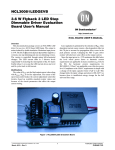
NCL30083FLYGEVB, NCL30083BB1GEVB 10 W Passive PFC Flyback and BuckBoost Dimmable LED Driver Evaluation Board User's Manual http://onsemi.com EVAL BOARD USER’S MANUAL Introduction This documentation package covers two NCL30083 LED driver implementations illustrating their use in an E26/E27 based A, PAR and BR LED lamps form factor. The Electronic Circuit Assembly (ECA) is designed to support either an isolated flyback or non-isolated buck-boost configuration. The nominal total power is 10 W for either application. The selection is controlled through selective component population of the ECA. Figure 1. NCL30083FLYGEVB − Flyback Figure 2. NCL30083BB1GEVB − Buck-Boost Table 1. DESIGN PARAMETER Input Voltage 100 – 265 V ac Line Frequency 50 Hz/60 Hz Power Factor > 0.7 Safety (Designed to Meet) IEC61347-2-13 EU UL8750 US Optimized Output Voltage Range Flyback (NCL30083FLYGEVB) Buck Boost (NCL30083BB1GEVB) 9.6 – 22.1 V dc 30 – 60 V dc Output Current Flyback (NCL30083FLYGEVB) Buck Boost (NCL30083BB1GEVB) 500 mA dc 195 mA dc Output Ripple Flyback (NCL30083FLYGEVB) Buck Boost (NCL30083BB1GEVB) 200 mA P-P 50 mA P-P Efficiency Flyback (NCL30083FLYGEVB) Buck Boost (NCL30083BB1GEVB) 85% 90% 2 % Typ. Start Up Time Semiconductor Components Industries, LLC, 2013 May, 2013 − Rev. 1 < 500 msec 1 Typ. Publication Order Number: EVBUM2179/D NCL30083FLYGEVB, NCL30083BB1GEVB Demo Board Modifications Since the NCL30082/3 has a wide VCC range this allows one transformer/inductor design to a > 2:1 change in LED string forward voltage. If it is desired to reduce the output current, the output power is no longer the limit, but simply the level of the reflected voltage from the auxiliary winding which is monitored by the built in overvoltage protection of the VCC pin. If a higher output voltage at lower current is required, the auxiliary winding turns ratio would have to be modified. The input capacitor network uses a valley fill PFC to achieve a power factor of > 0.8 to easily meet ENERGY STAR input power factor requirements. If compliance with EN61000-3-2 Class C is required, the input capacitor network can be easily modified and simplified to one capacitor, this is discussed in the appendix. The board as shipped contains the NCL30083 to demonstrate the line step dimming function which allows the LEDs to be dimmed in 5 discrete steps by toggling the AC line (Vin) off momentarily. Cvccbulk holds up VCC while Vin toggles low switching to the next lower dim level. Since the timing is user controlled by switching on/off the light switch the timing window is very wide. Toggling the AC input in one second is typical. It may take more than 20 seconds of AC off to reset the IC, at which time when turned on again it return to the 100% state. By removing the Cvccbulk the step dimming function is effectively disabled so the performance of the current control is just like the NCL300082. It is also possible with this board to replace the NCL30083 with an NCL30082 to evaluate the analog/ dimming control. The value of Rsense sets the final output current value in conjunction with Rtrim which is for fine adjustment. The nature of the primary side loop control makes the current adjustment somewhat iterative because several circuit parameters affect the output current setting. It is relatively easy by changing Rsense to increase the output of the evaluation board as long as the output power limit is considered. Constant Current Control Architecture Introduction Figure 4 portrays the primary and secondary current of a fly-back converter in discontinuous conduction mode (DCM). Figure 3 shows the basic circuit of a fly-back converter. Vbulk Transformer Lleak Cclp Nsp Rclp Vout . + Lp . Clamping Network Clump DRV Rsense Figure 3. Basic Flyback Converter Schematic N sp ǒV out ) V fǓ During the on-time of the MOSFET, the bulk voltage Vbulk is applied to the magnetizing and leakage inductors Lp and Lleak . The current ramps up. When the MOSFET is turned-off, the inductor current first charges Clump . The output diode is off until the voltage across Lp reverses and reaches: The output diode current increase is limited by the leakage inductor. As a consequence, the secondary peak current is reduced: http://onsemi.com 2 NCL30083FLYGEVB, NCL30083BB1GEVB I D,pk t at the auxiliary winding voltage, we can detect the end of the conduction time of secondary diode. The constant current control block picks up the leakage inductor current, the end of conduction of the output rectifier and controls the drain current to maintain the output current constant. We have: I L,pk N sp The diode current reaches its peak when the leakage inductor is reset. Thus, in order to accurately regulate the output current, we need to take into account the leakage inductor current. This is accomplished by sensing the clamping network current. Practically, a node of the clamp capacitor is connected to Rsense instead of the bulk voltage Vbulk . Then, by monitoring the voltage on the CS pin, we have an image of the primary current (red curve in Figure 4). When the diode conducts, the secondary current decreases linearly from ID,pk to zero. When the diode current has turned off, the drain voltage begins to oscillate because of the resonating network formed by the inductors (Lp + Lleak ) and the lump capacitor. This voltage is reflected on the auxiliary winding wired in fly-back mode. Thus, by looking I out + V REF 2N sp R sense (eq. 1) The output current value is set by choosing the sense resistor: R sense + V ref 2N sp I out (eq. 2) From (eq. 1), the first key point is that the output current is independent of the inductor value. Moreover, the leakage inductance does not influence the output current value as the reset time is taken into account by the controller. IL,pk Nsp ID,pk Ipri(t) Isec(t) Time t1 t2 tdemag ton Vaux(t) Time Figure 4. Flyback Currents and Auxiliary Winding Voltage in DCM At this point the Excel spreadsheet based design guide will help with many of the calculations. A trim resistor allows for making fine adjustments to the current limit to set the output current precisely. The LFF circuit will create some error on the Cs pin which is adjusted out by proper choice of Rtrim. So we will choose Rsense = 1.8 W and use Rtrim for the fine adjustments. After setting R4 to 1.1 kW, Rtrim is 22 W. http://onsemi.com 3 NCL30083FLYGEVB, NCL30083BB1GEVB SCHEMATIC Rdamp 180 W AC_L F1 D4 FUSE AC_N L2 AC1 + AC2 − C5 120 nF 400 V C4 18 mF 200 V D3 UFM15PL D2 UFM15PL MB6S L1 D1 220 mH UFM15PL C2 18 mF 200 V +HVDC C3 120 nF 400 V 1.5 mH Figure 5. Input Circuit Rclamp (FB Only) NOTE: Components labeled FB are only populated for the flyback version and components labeled BB are only required for the Buck-boost configuration Figure 6. Main Schematic http://onsemi.com 4 NCL30083FLYGEVB, NCL30083BB1GEVB Table 2. BILL OF MATERIALS Board Version Qty Designator FB BB Part Manufacturer Mfr Part Number Sub Pb-Free 1 CVccbulk x* x* 27 mF Panasonic EEU−FC1E270 Yes Yes 1 CVcc x x 4.7 mF Taiyo Yuden EMK107ABJ475KA−T Yes Yes 1 Cleak 1 Cout x 2 C2, C4 x 2 C3, C5 2 1 x 4.7 mF Rubycon 100YXJ4R7M5X11 Yes Yes 22 mF 16 V Taiyo Yuden EMK316BJ226ML−T Yes Yes x 18 mf 200 V Rubycon 200LLE18MEFC10X12.5 Yes Yes x x 120 nF 400 V Epcos B32559C6124+*** Yes Yes C10, C11 x x 1 nF Kemet C0402C102K3GACTU Yes Yes C13 x 1000 pF 630 V Kemet C0805C102KBRACTU Yes Yes 2 C14, C15 x 470 pF 250 VAC Y2 Johanson Dielectric 502R29W471KV3E−****−SC Yes Yes 4 D1, D2, D3, Dleak x 1 Dout x 1 D4 x 1 D9 1 F1 1 x UFM15PL MCC UFM15PL Yes Yes MURA220T3 On Semiconductor MURA220T3 No Yes x MB6S MCC MB6S Yes Yes x x BAS21DW5T1G ON Semiconductor BAS21DW5T1G No Yes x x FUSE Littelfuse 0263.500WRT1L Yes Yes L1 x x 220 mH Wurth 7447462221 Yes Yes 1 L2 x x 1.5 mH Wurth 7447462152 Yes Yes 1 Qfet x x NDD02N60Z ON Semiconductor NDD02N60Z No Yes 1 Rbo x x 3.01 MW Yageo RC0805FR−073M01L Yes Yes 1 Rclamp x 47 kW Yaego RC0805FR−0747K0L Yes Yes 1 Rdamp x x 180 W Yaego RC0805JR−07180RL Yes Yes 1 Rgd x x 10 W Yaego RC0603FR−0710RL Yes Yes 1 Rjump1 x* x* 0W Yaego RC0402JR−070RL Yes Yes 1 Rtco_trim x x 10 kW Yaego RC0402FR−0710KL Yes Yes 1 R8 x 10 kW Yaego RC0402FR−0710KL Yes Yes 0 Rjump2 * −* 10 kW Yaego RC0402FR−0710KL Yes Yes 1 Rlff x x 620 W Yaego RC0402FR−07620RL Yes Yes 1 Rsens x 0.68 W Yaego RL0603FR−070R68L Yes Yes RL0603FR−070R78L Yes Yes RC0805FR−071ML Yes Yes x 2 0.78 W Rstart1, Rstart x x 1.0 MW 1 Rtco x x 100 kW NTC Epcos B57331V2104J60 Yes Yes 1 Rtrim x 7.15 W Vishay/Dale CRCW06037R15FKEA Yes Yes 5.1 W Stackpole RMCF0603FT5R10 Yes Yes x Yageo 1 Rzcd x x 56 kW Yaego RC0805FR−0756KL Yes Yes 1 R2 x x 51.1 kW Yaego RC0402FR−0751K1L Yes Yes 1 R5 x x 4.7 W Yaego RC0805JR−074R7L Yes Yes 1 R9 x 100 W Yaego RC0805JR−07100RL Yes Yes 1 T1 x XFRM_LINEAR Wurth 750313435 No Yes 750313436 No Yes x 1 U1 x* x* NCL30083 ON Semiconductor NCL30083BDMR2G No Yes 2 Wire , Input, White x x UL1430 Alpha Wire #24 AWG, Stranded, 6 Yes Yes 1 Wire, Output, Red x x UL1430 Alpha Wire #24 AWG, Stranded, 6 Yes Yes 1 Wire, Output, Black x x UL1430 Alpha Wire #24 AWG, Stranded, 6 Yes Yes *To convert the board to NCL30082, the identified components are changed, see NCL30082 configuration table. http://onsemi.com 5 NCL30083FLYGEVB, NCL30083BB1GEVB Table 3. NCL30082 CONFIGURATION TABLE Topology Flyback (FB) Buck Boost (BB) Notes: Dimming Controller Cvccbulk Rjump1 Step Dimming NCL30083 X X No DIM Pin Access NCL30082 Remove Remove Access Dimming Pin NCL30082 Replace with Connector* Remove Step Dimming NCL30083 X X No DIM Pin Access NCL30082 Remove Remove Access Dimming Pin NCL30082 Replace with Connector* Remove Connector Assembly Supplier Part Number * Board Connector Molex 22035025 Mating Connector Molex 50375023 Connector Terminal Molex 8701039 GERBER VIEWS Figure 7. Top Side PCB Figure 8. Bottom Side PCB http://onsemi.com 6 Rjump2 X X NCL30083FLYGEVB, NCL30083BB1GEVB Figure 9. Top Silkscreen Figure 10. Bottom Silkscreen CIRCUIT BOARD FABRICATION NOTES 11. Size tolerance of plated holes: 0.003 in.: non-plated holes 0.002 in. 12. All holes shall be 0.003 in. of their true position U.D.S. 13. Construction to be SMOBC, using liquid photo image (LPI) solder mask in accordance with IPC−SM−B40C, Type B, Class 2, and be green in color. 14. Solder mask misregistration 0.004 in. max. 15. Silkscreen shall be permanent non-conductive white ink. 16. The fabrication process shall be UL approved and the PCB shall have a flammability rating of UL94V0 to be marked on the solder side in silkscreen with date, manufactures approved logo, and type designation. 17. Warp and twist of the PCB shall not exceed 0.0075 in. per in. 18. 100% electrical verification required. 19. Surface finish: electroless nickel immersion gold (ENIG) 20. RoHS compliance required. 1. Fabricate per IPC−6011 and IPC6012. Inspect to IPA−A−600 Class 2 or updated standard. 2. Printed Circuit Board is defined by files listed in fileset. 3. Modification to copper within the PCB outline is not allowed without permission, except where noted otherwise. The manufacturer may make adjustments to compensate for manufacturing process, but the final PCB is required to reflect the associated gerber file design 0.001 in. for etched features within the PCB outline. 4. Material in accordance with IPC−4101/21, FR4, Tg 125C min. 5. Layer to layer registration shall not exceed 0.004 in. 6. External finished copper conductor thickness shall be 0.0013 in. min. 7. Copper plating thickness for through holes shall be 0.0007 in. min. 8. All holes sizes are finished hole size. 9. Finished PCB thickness 0.031 in. 10. All undimensioned holes to be drilled using the NC drill data. http://onsemi.com 7 NCL30083FLYGEVB, NCL30083BB1GEVB FLYBACK TRANSFORMER SPECIFICATION CUSTOMER TERMINAL RoHS LEAD(Pb)-FREE Sn 96%, Ag 4% Yes Yes PART MUST INSERT FULLY TO SURFACE A IN RECOMMENDED GRID .530 Max. [13.46] DOT LOCATES TERM. #1 .837 Max. [21.50] .110 MIN [2.79] FL1 .800 Max. [20.32] FL2 TERM. NO.’S FOR REF. ONLY 4 PRI 120−375 V 100 kHz FL1 FL2 LOT CODE & DATE CODE .600 [15.24] .047(4) [1.20] FL2 SEC 14 V−700 mV 3 750313435 .020 SQ(4) [.50] −A− .200(1) [5.08] FL1 .150(2) [3.81] 1 AUX 16 V−10 mA RECOMMENDED P.C. PATTERN, COMPONENT SIDE 2 ELECTRICAL SPECIFICATIONS @ 255C unless otherwise noted: D.C. RESISTANCE (@ 20C): 1−2 1.25 W 10%. 3−4, 0.695 W 10%. FL1−FL2, 0.090 W 20%. DIELECTRIC RATING: 3,000 VAC, 1 minute tested by applying 3,750 VAC for 1 second between pins 4−FL1 (tie 2+3). 500 VAC, 1 minute tested by applying 625 VAC for 1 second between pins 1−4. INDUCTANCE: 700 mH 10%, 10 kHz, 100 mVAC, 0 mADC, 3−4, Ls. SATURATION CURRENT: 1 A saturating current that causes 20% rolloff from initial inductance. LEAKAGE INDUCTANCE 5.0 mH max, 100 kHz, 100 mVAC, 1−2 (tie FL1+FL2), Ls. 15.0 mH max, 100 kHz, 100 mVAC, 3−4 (tie FL1+FL2), Ls. TURNS RATIO: (4−3):(1−2), (2.5):(1.00), 1%. (4−3):(FL1−FL2), (3):(1.00), 1%. OPERATING TEMPERATURE RANGE: −40C TO 125C including temp. rise. Unless otherwise specified, tolerances are as follows: Angles: 1 Fractions: 1/64 This drawing is dual dimensioned. Dimensions in brackets are in millimeters. http://onsemi.com 8 Decimals: 0.005 (.127 mm) NCL30083FLYGEVB, NCL30083BB1GEVB BUCK BOOST INDUCTOR SPECIFICATION CUSTOMER TERMINAL RoHS LEAD(Pb)-FREE Sn 96%, Ag 4% Yes Yes PART MUST INSERT FULLY TO SURFACE A IN RECOMMENDED GRID .530 Max. [13.46] DOT LOCATES TERM. #1 .837 Max. [21.50] .110 MIN [2.79] .800 Max. [20.32] TERM. NO.’S FOR REF. ONLY 750313436 .020 SQ(4) [.50] −A− LOT CODE & DATE CODE 4 .600 [15.24] .047(4) [1.20] PRI 120−375 V 100 kHz .200(1) [5.08] 3 1 .150(2) [3.81] AUX 16 V−10 mA 2 RECOMMENDED P.C. PATTERN, COMPONENT SIDE ELECTRICAL SPECIFICATIONS @ 255C unless otherwise noted: D.C. RESISTANCE (@ 20C): 1−2 0.450 W 10%. 3−4, 0.965 W 10%. DIELECTRIC RATING: 1,000 VAC, 1 minute tested by applying 1,250 VAC for 1 second between pins 1−4. INDUCTANCE: 950 mH 10%, 10 kHz, 100 mVAC, 0 mADC, 3−4, Ls. SATURATION CURRENT: 1 A saturating current that causes 20% rolloff from initial inductance. LEAKAGE INDUCTANCE 25.0 mH max, 100 kHz, 100 mVAC, 3−4 (tie 1+2), Ls. TURNS RATIO: (4−3):(1−2), (3):(1.00), 1%. OPERATING TEMPERATURE RANGE: −40C TO 125C including temp. rise. Unless otherwise specified, tolerances are as follows: Angles: 1 Fractions: 1/64 This drawing is dual dimensioned. Dimensions in brackets are in millimeters. http://onsemi.com 9 Decimals: 0.005 (.127 mm) NCL30083FLYGEVB, NCL30083BB1GEVB FLYBACK ECA PICTURES Output Lead Breakout Cleak − Unstuffed on Flyback Figure 11. Flyback Top View Figure 12. Flyback Bottom View http://onsemi.com 10 NCL30083FLYGEVB, NCL30083BB1GEVB BUCK BOOST ECA PICTURES Output Lead Breakout Figure 13. Buck Boost Top View Parts Unstuffed on Buck Boost Figure 14. Buck Boost Bottom View http://onsemi.com 11 NCL30083FLYGEVB, NCL30083BB1GEVB Note location of transformer Flying Leads trim as short as possible. Mark the Appropriate Configuration Figure 15. Flyback Lead Breakout Figure 16. Buck Boost Lead Breakout http://onsemi.com 12 NCL30083FLYGEVB, NCL30083BB1GEVB TEST PROCEDURE Equipment Needed AC Source – 100 to 265 V ac 50/60 Hz Minimum 1 A ac capabilities AC Wattmeter – 30 W Minimum, True RMS Input Flyback – 14–17 V dc – 5 LED Load @ 500mA Buck Boost – 50–55 V dc – 15 LED Load @ 200 mA Test Connections Voltage and Current, Power Factor 0.2% accuracy or better DC Voltmeter – 100 V dc minimum 0.1% accuracy or better DC Ammeter – 1 A dc minimum 0.1% accuracy or better LED Load 1. Connect the Unit Under Test (UUT) per the test set up in Figure 17. 2. Set the AC source to 120 1 V ac RMS 60 Hz or 230 2 V ac RMS 50 Hz. NOTE: Unless otherwise specified, all voltage measurements are taken at the terminals of the UUT. DC Ammeter AC Power Source AC Wattmeter UUT DC Voltmeter LED Test Load Figure 17. Test Set Up Functional Test Procedure Table 4. FLYBACK VERSION (NCL30083FLYGEVB) Test Limits Test Condition Test Variable Min Max Vin = 100 V ac Output Current 490 mA 510 mA Vin = 120 V ac Output Current 490 mA 510 mA Vin = 265 V ac Output Current 490 mA 510 mA Vin = 265 V ac Power Factor 0.70 Vin = 120 V ac Vout = 14 V Efficiency (Use Actual Measured Data) 82% Pass/Fail Table 5. BUCK BOOST VERSION (NCL30083BB1GEVB) Test Limits Test Condition Test Variable Min Max Vin = 100 V ac Output Current 190 mA 200 mA Vin = 120 V ac Output Current 190 mA 200 mA Vin = 265 V ac Output Current 190 mA 200 mA Vin = 265 V ac Power Factor 0.70 Vin = 120 V ac Vout = 55 V Efficiency (Use Actual Measured Data) 87% Pass/Fail Efficiency = ((VOUT IOUT) / Pin) 100% Step Dimming Test Procedure NCL30083BB1GEVB/NCL30083FLYGEVB 4. Interrupting the AC input for 1−2 s will step the output current down. 5. There 6 discrete current levels. After the lowest level, the current will return to maximum output. 6. Cycle the input power 6 times validating that the current steps down at each cycle and returns to maximum. 1. Connect the UUT to the LED load. 2. Apply 120 V ac power. 3. Verify that the output current is within the regulation limits as specified in the functional test procedure. http://onsemi.com 13 NCL30083FLYGEVB, NCL30083BB1GEVB TEST DATA 510 508 Output Current (mA) 506 504 502 9.6 V LED Vf 500 22.1 V LED Vf 498 496 494 492 490 90 115 140 165 190 215 240 265 Line Voltage (V ac) Figure 18. Flyback Line & Load Regulation 2.0% 1.5% Line Regulation 1.0% 0.5% 0.0% -0.5% -1.0% 3 LED 6 LED -1.5% -2.0% 90 115 140 4 LED 7 LED 165 190 5 LED 215 240 Line Voltage (V ac) Figure 19. Flyback Relative Line Regulation http://onsemi.com 14 265 NCL30083FLYGEVB, NCL30083BB1GEVB 89% 88% Efficiency 87% 86% 85% 84% 3 LED 6 LED 83% 82% 90 115 4 LED 7 LED 140 165 5 LED 190 215 240 265 Line Voltage (V ac) Figure 20. Flyback Line & Load Efficiency 0.95 0.90 9.6 V LED Vf Power Factor 0.85 22.1 V LED Vf 0.80 0.75 0.70 0.65 90 115 140 165 190 215 240 Line Voltage (V ac) Figure 21. Flyback Line & Load Power Factor http://onsemi.com 15 265 NCL30083FLYGEVB, NCL30083BB1GEVB 0.60 0.58 0.56 Output Current (A) 0.54 0.52 0.50 0.48 0.46 0.44 0.42 0.40 0 2 4 6 8 10 12 14 16 18 20 Time (ms) Figure 22. Flyback Output Ripple 120 V ac 60 Hz 0.55 0.54 Output Current (A) 0.53 0.52 0.51 0.50 0.49 0.48 0.47 0.46 0.45 0 2 4 6 8 10 12 14 16 Time (ms) Figure 23. Flyback Output Ripple 230 V ac 50 Hz http://onsemi.com 16 18 20 NCL30083FLYGEVB, NCL30083BB1GEVB 200 199 197 196 195 194 193 29V LED Vf 192 60 V LED Vf 191 190 100 120 140 160 180 200 220 240 260 Line Voltage Figure 24. Buck Boost Line & Load Regulation 93.0% 92.5% 92.0% Efficiency Output Current (mA) 198 91.5% 91.0% 90.5% 90.0% 100 120 140 160 180 200 220 240 260 Line Voltage (V ac) Figure 25. Buck Boost Efficiency over Line (V1 = 55 V/Iout = 195 mA) http://onsemi.com 17 NCL30083FLYGEVB, NCL30083BB1GEVB 0.85 0.84 Power Factor 0.83 0.82 0.81 0.80 0.79 0.78 100 120 140 160 180 200 220 240 260 Line Voltage (V ac) Figure 26. Buck Boost Power Factor over Line (V1 = 55 V/Iout = 195 mA) 0.210 0.208 0.206 Output Current (A) 0.204 0.202 0.200 0.198 0.196 0.194 0.192 0.190 0.188 0.186 0 2 4 6 8 10 12 14 16 18 Time (ms) Figure 27. Buck Boost Output Ripple 120 V ac 60 Hz http://onsemi.com 18 20 NCL30083FLYGEVB, NCL30083BB1GEVB 0.210 0.208 Output Current (A) 0.206 0.204 0.202 0.200 0.198 0.196 0.194 0.192 0.190 0 2 4 6 8 10 12 14 16 18 Time (ms) Figure 28. Buck Boost Output Ripple 230 V ac 50 Hz Figure 29. Conducted EMI Pre-compliance 150 kHz−2 MHz http://onsemi.com 19 20 NCL30083FLYGEVB, NCL30083BB1GEVB Figure 30. Conducted EMI Pre-compliance 150 kHz−30 MHz APPENDIX IEC61000−3−2 Class C Compliance peaks per half period) before or at 65 and does not stop flowing before 90, where the zero crossing of the fundamental supply voltage is assumed to be at 0. Compliance to IEC61000−3−2 Class C (under 25 W) is not possible with the valley fill front end architecture since input current does not comply with Class D requirements or the waveform definition requirements as stated in this excerpt. If the discharge lighting equipment has a built-in dimming device, measurement is made only in the full load condition. It is possible to comply with the special waveform and harmonic requirements of the third paragraph with a standard peak charge front end if the bulk capacitance is properly sized. The bulk capacitor must be in the range of 200−300 nF/W for a 230 V ac line for Europe. Japan has a similar requirement; however, the bulk capacitance must be 800–1,200 nF/W because the nominal main is 100 V ac rather than 230 V ac. The recommended capacitance values are line specific. So there is no universal mains solution with a peak charge front end. It is possible to convert the Evaluation Board from a valley fill to peak charge front end by deleting, changing, and shorting selected components. Active Input Power 3 25 W: Discharge lighting equipment having an active input power smaller than or equal to 25 W shall comply with one of the following two sets of requirements: The harmonic currents shall not exceed the power-related limits of Table 6, column 2, or: The third harmonic current, expressed as a percentage of the fundamental current, shall not exceed 86% and the fifth shall not exceed 61%; moreover, the waveform of the input current shall be such that it begins to flow before or at 60, has its last peak (if there are several http://onsemi.com 20 NCL30083FLYGEVB, NCL30083BB1GEVB Rdamp Delete D1, D3, & C2 180 W AC_L F1 D4 FUSE AC_N L2 AC1 + AC2 − C5 120 nF 400 V L1 D1 220 mH UFM15PL C4 18 mF 200 V D2 UFM15PL D3 UFM15PL MB6S 1.5 mH +HVDC C3 120 nF 400 V C2 18 mF 200 V Short D2 Figure 31. Peak Charge Conversion for Evaluation Board Table 6. BULK CAPACITOR SELECTION TABLE NOTE: Line Minimum Capacitance Maximum Capacitance Voltage Rating 230 V ac 50 Hz 2.2 mF 3.3 mF 400 V dc 100 V ac 50/60 Hz 8.2 mF 12 mF 200 V dc Capacitance values based on 10 W output and selected to the nearest standard value. To illustrate Class C performance, an NCL30083FLYGEVB was modified and the input valley fill configuration was modified and the input bulk capacitor was changed to 2.2 mF, this is the typical performance data. Typical harmonic content is illustrated in Figure 34. For applications with 4 LEDs or less, the input capacitor value should be reduced to meet Class C harmonic content requirements. 1.5% Relative Current Regulation 1.0% 0.5% 0.0% -0.5% 5 LED -1.0% 6 LED 7 LED -1.5% 180 190 200 210 220 230 240 250 260 Line Voltage (V ac) Figure 32. 230 V ac, Class C − Flyback Relative Current Regulation http://onsemi.com 21 270 NCL30083FLYGEVB, NCL30083BB1GEVB 87.0% 86.5% Efficiency 86.0% 85.5% 85.0% 5 LED 6 LED 7 LED 84.5% 84.0% 180 190 200 210 220 230 240 250 260 270 Line Voltage (Vac) Figure 33. 230 V ac, Class C − Flyback Line & Load Efficiency Power Factor 3rd Harmonic 5th Harmonic 5 LED 0.575 81% 52.4% 6 LED 0.587 78% 47.0% 7 LED 0.59 74.6% 40.6% Class C Limit − 86% 61% Figure 34. Class C − Measured Harmonic Content. Vin = 230 V ac, 50 Hz ENERGY STAR and the ENERGY STAR mark are registered U.S. Marks. Microsoft Excel is a registered trademark of Microsoft Corporation. ON Semiconductor and are registered trademarks of Semiconductor Components Industries, LLC (SCILLC). SCILLC owns the rights to a number of patents, trademarks, copyrights, trade secrets, and other intellectual property. A listing of SCILLC’s product/patent coverage may be accessed at www.onsemi.com/site/pdf/Patent−Marking.pdf. SCILLC reserves the right to make changes without further notice to any products herein. SCILLC makes no warranty, representation or guarantee regarding the suitability of its products for any particular purpose, nor does SCILLC assume any liability arising out of the application or use of any product or circuit, and specifically disclaims any and all liability, including without limitation special, consequential or incidental damages. “Typical” parameters which may be provided in SCILLC data sheets and/or specifications can and do vary in different applications and actual performance may vary over time. All operating parameters, including “Typicals” must be validated for each customer application by customer’s technical experts. SCILLC does not convey any license under its patent rights nor the rights of others. SCILLC products are not designed, intended, or authorized for use as components in systems intended for surgical implant into the body, or other applications intended to support or sustain life, or for any other application in which the failure of the SCILLC product could create a situation where personal injury or death may occur. Should Buyer purchase or use SCILLC products for any such unintended or unauthorized application, Buyer shall indemnify and hold SCILLC and its officers, employees, subsidiaries, affiliates, and distributors harmless against all claims, costs, damages, and expenses, and reasonable attorney fees arising out of, directly or indirectly, any claim of personal injury or death associated with such unintended or unauthorized use, even if such claim alleges that SCILLC was negligent regarding the design or manufacture of the part. SCILLC is an Equal Opportunity/Affirmative Action Employer. This literature is subject to all applicable copyright laws and is not for resale in any manner. PUBLICATION ORDERING INFORMATION LITERATURE FULFILLMENT: Literature Distribution Center for ON Semiconductor P.O. Box 5163, Denver, Colorado 80217 USA Phone: 303−675−2175 or 800−344−3860 Toll Free USA/Canada Fax: 303−675−2176 or 800−344−3867 Toll Free USA/Canada Email: [email protected] N. American Technical Support: 800−282−9855 Toll Free USA/Canada Europe, Middle East and Africa Technical Support: Phone: 421 33 790 2910 Japan Customer Focus Center Phone: 81−3−5817−1050 http://onsemi.com 22 ON Semiconductor Website: www.onsemi.com Order Literature: http://www.onsemi.com/orderlit For additional information, please contact your local Sales Representative EVBUM2179/D