1
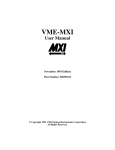
AT-MXI
User Manual
bus
February 1994 Edition
Part Number 320339-01
© Copyright 1992, 1994 National Instruments Corporation.
All Rights Reserved.
National Instruments Corporate Headquarters
6504 Bridge Point Parkway
Austin, TX 78730-5039
(512) 794-0100
Technical support fax: (800) 328-2203
(512) 794-5678
Branch Offices:
Australia (03) 879 9422, Austria (0662) 435986, Belgium 02/757.00.20, Canada (Ontario) (519) 622-9310,
Canada (Québec) (514) 694-8521, Denmark 45 76 26 00, Finland (90) 527 2321, France (1) 48 14 24 24,
Germany 089/741 31 30, Italy 02/48301892, Japan (03) 3788-1921, Netherlands 03480-33466, Norway 32-848400,
Spain (91) 640 0085, Sweden 08-730 49 70, Switzerland 056/20 51 51, U.K. 0635 523545
Limited Warranty
The AT-MXI is warranted against defects in materials and workmanship for a period of one year from the date of
shipment, as evidenced by receipts or other documentation. National Instruments will, at its option, repair or replace
equipment that proves to be defective during the warranty period. This warranty includes parts and labor.
A Return Material Authorization (RMA) number must be obtained from the factory and clearly marked on the
outside of the package before any equipment will be accepted for warranty work. National Instruments will pay the
shipping costs of returning to the owner parts which are covered by warranty.
National Instruments believes that the information in this manual is accurate. The document has been carefully
reviewed for technical accuracy. In the event that technical or typographical errors exist, National Instruments
reserves the right to make changes to subsequent editions of this document without prior notice to holders of this
edition. The reader should consult National Instruments if errors are suspected. In no event shall National
Instruments be liable for any damages arising out of or related to this document or the information contained in it.
EXCEPT AS SPECIFIED HEREIN, N ATIONAL INSTRUMENTS MAKES NO WARRANTIES, EXPRESS OR IMPLIED,
AND SPECIFICALLY DISCLAIMS ANY WARRANTY OF MERCHANTABILITY OR FITNESS FOR A PARTICULAR
PURPOSE . CUSTOMER'S RIGHT TO RECOVER DAMAGES CAUSED BY FAULT OR NEGLIGENCE ON THE PART
OF NATIONAL INSTRUMENTS SHALL BE LIMITED TO THE AMOUNT THERETOFORE PAID BY THE CUSTOMER.
NATIONAL INSTRUMENTS WILL NOT BE LIABLE FOR DAMAGES RESULTING FROM LOSS OF DATA, PROFITS,
USE OF PRODUCTS, OR INCIDENTAL OR CONSEQUENTIAL DAMAGES, EVEN IF ADVISED OF THE POSSIBILITY
THEREOF. This limitation of the liability of National Instruments will apply regardless of the form of action,
whether in contract or tort, including negligence. Any action against National Instruments must be brought within
one year after the cause of action accrues. National Instruments shall not be liable for any delay in performance due
to causes beyond its reasonable control. The warranty provided herein does not cover damages, defects,
malfunctions, or service failures caused by owner's failure to follow the National Instruments installation, operation,
or maintenance instructions; owner's modification of the product; owner's abuse, misuse, or negligent acts; and
power failure or surges, fire, flood, accident, actions of third parties, or other events outside reasonable control.
Copyright
Under the copyright laws, this publication may not be reproduced or transmitted in any form, electronic or
mechanical, including photocopying, recording, storing in an information retrieval system, or translating, in whole or
in part, without the prior written consent of National Instruments Corporation.
Trademarks
LabVIEW ® and NI-VXI™ are trademarks of National Instruments Corporation.
Product and company names listed are trademarks or trade names of their respective companies.
Warning Regarding Medical and Clinical Use
of National Instruments Products
National Instruments products are not designed with components and testing intended to ensure a level of reliability
suitable for use in treatment and diagnosis of humans. Applications of National Instruments products involving
medical or clinical treatment can create a potential for accidental injury caused by product failure, or by errors on the
part of the user or application designer. Any use or application of National Instruments products for or involving
medical or clinical treatment must be performed by properly trained and qualified medical personnel, and all
traditional medical safeguards, equipment, and procedures that are appropriate in the particular situation to prevent
serious injury or death should always continue to be used when National Instruments products are being used.
National Instruments products are NOT intended to be a substitute for any form of established process, procedure, or
equipment used to monitor or safeguard human health and safety in medical or clinical treatment.
FCC/DOC Radio Frequency Interference Compliance
This equipment generates and uses radio frequency energy and, if not installed and used in strict accordance with the
instructions in this manual, may cause interference to radio and television reception. This equipment has been tested
and found to comply with the following two regulatory agencies:
Federal Communications Commission
This device complies with Part 15 of the Federal Communications Commission (FCC) Rules for a Class A digital
device. Operation is subject to the following two conditions:
1.
This device may not cause harmful interference in commercial environments.
2.
This device must accept any interference received, including interference that may cause undesired operation.
Canadian Department of Communications
This device complies with the limits for radio noise emissions from digital apparatus set out in the Radio
Interference Regulations of the Canadian Department of Communications (DOC).
Le présent appareil numérique n’émet pas de bruits radioélectriques dépassant les limites applicables aux appareils
numériques de classe A prescrites dans le règlement sur le brouillage radioélectrique édicté par le ministère des
communications du Canada.
Instructions to Users
These regulations are designed to provide reasonable protection against harmful interference from the equipment to
radio reception in commercial areas. Operation of this equipment in a residential area is likely to cause harmful
interference, in which case the user will be required to correct the interference at his own expense.
There is no guarantee that interference will not occur in a particular installation. However, the chances of
interference are much less if the equipment is installed and used according to this instruction manual.
If the equipment does cause interference to radio or television reception, which can be determined by turning the
equipment on and off, one or more of the following suggestions may reduce or eliminate the problem.
•
Operate the equipment and the receiver on different branches of your AC electrical system.
•
Move the equipment away from the receiver with which it is interfering.
•
Reorient or relocate the receiver’s antenna.
•
Be sure that the equipment is plugged into a grounded outlet and that the grounding has not been defeated with a
cheater plug.
Notice to user: Changes or modifications not expressly approved by National Instruments could void the user’s
authority to operate the equipment under the FCC Rules.
If necessary, consult National Instruments or an experienced radio/television technician for additional suggestions.
The following booklet prepared by the FCC may also be helpful: How to Identify and Resolve Radio-TV
Interference Problems. This booklet is available from the U.S. Government Printing Office, Washington, DC
20402, Stock Number 004-000-00345-4.
Contents
About This Manual .............................................................................................................. xi
Organization of the AT-MXI User Manual .................................................................... xi
Conventions Used in This Manual .................................................................................. xii
How to Use This Manual ................................................................................................ xii
Related Documentation ................................................................................................... xii
Customer Communication .............................................................................................. xii
Chapter 1
Introduction to MXIbus ...................................................................................................1-1
Overview ........................................................................................................................1-1
The Need for MXIbus ....................................................................................................1-1
VXI Connection .............................................................................................................1-2
MXIbus Applications .....................................................................................................1-3
MXIbus – An Open Standard.........................................................................................1-5
MXIbus Operation .........................................................................................................1-5
MXIbus Signals..............................................................................................................1-5
MXIbus Cables ..............................................................................................................1-5
MXIbus Termination......................................................................................................1-7
MXIbus Performance .....................................................................................................1-7
Data Transfer Rates........................................................................................................1-8
MXIbus Data Rates ........................................................................................................1-8
Local Performance .........................................................................................................1-9
Chapter 2
General Information ..........................................................................................................2-1
Overview ........................................................................................................................2-1
What Your Kit Should Contain......................................................................................2-2
Optional Hardware .........................................................................................................2-3
Optional Software ..........................................................................................................2-3
Chapter 3
Configuration and Installation .......................................................................................3-1
Step 1. Unpack the AT-MXI ..........................................................................................3-1
Step 2. Configure the AT-MXI ......................................................................................3-1
Switch and Jumper Settings ...............................................................................3-3
Base I/O Address Selection................................................................................3-3
Interrupt Level Selection....................................................................................3-6
DMA Channel Selection ....................................................................................3-8
Master Mode Versus Slave Mode ..........................................................3-8
MXIbus Termination Option .............................................................................3-10
Step 3. Install the AT-MXI ............................................................................................3-12
Step 4. Connect the AT-MXI to the MXIbus.................................................................3-13
© National Instruments Corporation
vii
AT-MXI User Manual
Contents
Chapter 4
Register Descriptions .........................................................................................................4-1
Register Map ..................................................................................................................4-1
Register Description Format ..............................................................................4-3
Slave Mode Address Register ............................................................................4-4
Slave Mode Address Mapping Register.............................................................4-6
Master Mode Address Page Register .................................................................4-8
Master Mode Address Modifier and Enable Register........................................4-9
Signal Register ...................................................................................................4-12
Board Status Register .........................................................................................4-13
Board Control Register ......................................................................................4-17
Slave Mode Timer Register ...............................................................................4-21
Master Mode Timer Register .............................................................................4-22
System Controller Timer Register .....................................................................4-23
Timer Control Register ......................................................................................4-24
Chapter 5
Programming Considerations ........................................................................................5-1
Initialization ...................................................................................................................5-1
Initializing the Timers ........................................................................................5-1
Programming the AT-MXI to be the MXIbus System Controller .....................5-3
Initializing the AT-MXI for Slave-Mode Operation..........................................5-3
Initializing the Master-Mode Window...............................................................5-4
Master-Mode Operation .................................................................................................5-5
Paging.................................................................................................................5-6
Deadlock ............................................................................................................5-7
Timing Incompatibilities ....................................................................................5-8
Performing MXIbus Block-Mode Transfers ......................................................5-8
Using a Processor for MXIbus Blocks...................................................5-9
Using the System DMA Controller for MXIbus Blocks........................5-9
Performing MXIbus Indivisible Transfers .........................................................5-10
Channel I/O Transfers ............................................................................5-10
Read-Modify-Write Cycles ....................................................................5-11
Locking the MXIbus ..........................................................................................5-11
Slave-Mode Operation ...................................................................................................5-12
Locking the PC AT Bus .....................................................................................5-12
Using the AT-MXI Communication Registers ..............................................................5-13
AT-MXI Interrupts.........................................................................................................5-15
Chapter 6
Theory of Operation ..........................................................................................................6-1
AT-MXI Functional Description ...................................................................................6-1
MXIbus Terminators ..........................................................................................6-3
System Controller Logic ....................................................................................6-3
Address Modifier, Address/Data, MXIbus Control Transceivers......................6-3
Master-Mode Address Modifier Register ..........................................................6-3
Slave-Mode Address Latch/Counter ..................................................................6-3
Slave-Mode Address Decoder ...........................................................................6-4
Slave-Mode Offset Register ...............................................................................6-4
Slave-Mode State Machine ................................................................................6-4
Master-Mode Address Latch..............................................................................6-4
Master-Mode Address Decoder .........................................................................6-4
AT-MXI User Manual
viii
© National Instruments Corporation
Contents
Master-Mode Address Page Register.................................................................6-5
Master-Mode State Machine ..............................................................................6-5
Parity Generator/Checker...................................................................................6-5
Data Latch/Byte Swapper ..................................................................................6-5
Communication Registers ..................................................................................6-5
Interrupt Circuitry ..............................................................................................6-5
PC AT Address, Data and Control Transceivers ...............................................6-6
Master-Mode Operation .................................................................................................6-6
MXIbus Arbitration............................................................................................6-6
MXIbus Address Broadcast ...............................................................................6-7
Master-Mode Data Transfer ...............................................................................6-8
Master-Mode Cycle Termination .......................................................................6-9
Slave-Mode Operation ...................................................................................................6-10
Slave-Mode Address Mapping...........................................................................6-10
PC AT Bus Arbitration ......................................................................................6-10
Slave-Mode Data Transfer .................................................................................6-11
Slave-Mode Block Transfers .................................................................6-12
Slave-Mode Cycle Termination .........................................................................6-12
Appendix A
Specifications ........................................................................................................................A-1
Appendix B
Mnemonics .............................................................................................................................B-1
Appendix C
MXIbus Connector Description ....................................................................................C-1
Appendix D
Customer Communication ..............................................................................................D-1
Glossary ...................................................................................................................... Glossary-1
Index ..................................................................................................................................Index-1
© National Instruments Corporation
ix
AT-MXI User Manual
Contents
Figures
Figure
Figure
Figure
Figure
Figure
1-1.
1-2.
1-3.
1-4.
1-5.
Comparison of Data Transfer Rates ....................................................................1-2
PC Using MXI to Control VXIbus or VMEbus ..................................................1-3
MXI Used for Multiple Mainframe VXIbus or VMEbus System .......................1-4
MXI Used for High-Speed Shared-Memory Network ........................................1-4
MXIbus Multi-Drop Cable Assembly .................................................................1-6
Figure 2-1.
AT-MXI Interface Board .....................................................................................2-1
Figure
Figure
Figure
Figure
Figure
AT-MXI Parts Locator Diagram .........................................................................3-2
Base I/O Address Switch Settings .......................................................................3-4
Board and MXIbus Interrupt Jumper Settings .....................................................3-7
DMA Channel Settings ........................................................................................3-10
MXIbus Terminating Networks...........................................................................3-11
3-1.
3-2.
3-3.
3-4.
3-5.
Figure 6-1.
Figure 6-2.
AT-MXI Block Diagram .....................................................................................6-2
Byte-Swapping Circuitry .....................................................................................6-8
Figure C-1. MXIbus Connector ..............................................................................................C-1
Tables
Table 3-1.
Table 3-2.
AT-MXI Factory Default Settings and Optional Configurations ........................3-3
Possible Base I/O Address Settings for the AT-MXI ..........................................3-5
Table 4-1.
Table 4-2.
AT-MXI Register Map ........................................................................................4-2
Address Modifier Codes ......................................................................................4-10
Table 5-1.
AT-MXI Timers...................................................................................................5-2
Table 6-1.
Table 6-2.
PC AT Control Signals and MXIbus Control Signals .........................................6-7
Slave-Mode Transfer Types on the AT-MXI ......................................................6-11
Table C-1. MXIbus Connector Signal Assignments .............................................................C-1
Table C-2. MXIbus Signal Groupings ...................................................................................C-2
AT-MXI User Manual
x
© National Instruments Corporation
About This Manual
The AT-MXI User Manual describes the functional, physical, and electrical aspects of the
AT-MXI and contains information concerning its operation and programming.
Organization of the AT-MXI User Manual
The AT-MXI User Manual is organized as follows:
•
Chapter 1, Introduction to MXI, is a tutorial of MXIbus concepts.
•
Chapter 2, General Information, contains an overview of the functionality of the AT-MXI
interface board, shows a picture of the AT-MXI board, and lists the contents of your kit and
available optional equipment.
•
Chapter 3, Configuration and Installation, describes the procedures for unpacking,
configuring, and installing your AT-MXI interface board.
•
Chapter 4, Register Descriptions, contains detailed information on the use of the AT-MXI
registers that are accessible via the PC AT bus using I/O operations.
•
Chapter 5, Programming Considerations, contains information on how to program the
AT-MXI interface registers.
•
Chapter 6, Theory of Operation, contains a functional block diagram of the AT-MXI, a brief
description of the major elements of the interface board, and a detailed description of both
master-mode and slave-mode operation.
•
Appendix A, Specifications, lists various module specifications of the AT-MXI, such as
physical dimensions and power requirements.
•
Appendix B, Mnemonics Key, contains an alphabetical listing of mnemonics used in this
manual to describe signals, registers, and register bits. Refer also to the Acronyms section
later in this Preface.
•
Appendix C, MXIbus Connector Description, describes the connector pin assignments for the
MXIbus connector.
•
Appendix D, Customer Communication, contains forms for you to complete to facilitate
communication with National Instruments concerning our products.
•
The Glossary contains an alphabetical list and description of terms used in this manual,
including abbreviations, acronyms, metric prefixes, and symbols.
•
The Index contains an alphabetical list of key terms and topics used in this manual, including
the page where each one can be found.
© National Instruments Corporation
xi
AT-MXI User Manual
About This Manual
Conventions Used in This Manual
The following conventions are used in this manual.
italic
Italic text denotes emphasis, a cross reference, or an introduction to a key
concept.
monospace
Txt in this font denotes sections of code.
bold italic
Bold italic text denotes a note, caution, or warning.
Abbreviations, acronyms, metric prefixes, symbols, and terms are listed in the Glossary.
How to Use This Manual
You should begin with Chapter 1 to gain an understanding of MXIbus concepts. This chapter
explains how MXIbus devices attach together and communicate with each other. Chapter 2
contains a general overview about the AT-MXI board. Chapter 3 contains information on how to
configure and install your AT-MXI into an AT-based computer. Chapters 4 and 5 contain
information you will need to program your AT-MXI. You can skip these chapters if you are
using a compatible National Instruments software package because the software routines perform
these functions automatically. Chapter 6 contains more technical information on the use of the
AT-MXI.
Related Documentation
The following manuals contain information that you may find helpful as you read the AT-MXI
User Manual:
•
Multisystem Extension Interface Bus Specification, Version 1.2 (part number 340007-01)
•
VXIbus System Specification, Revision 1.4, VXIbus Consortium (available from National
Instruments, part number 350083-01)
Customer Communication
National Instruments wants to receive your comments on our products and manuals. We are
interested in the applications you develop with our products, and we want to help if you have
problems with them. To make it easy for you to contact us, this manual contains comment and
configuration forms for you to complete. These forms are in Appendix D, Customer
Communication, at the end of this manual.
AT-MXI User Manual
xii
© National Instruments Corporation
Chapter 1
Introduction to MXIbus
Overview
The MXIbus (Multisystem Extension Interface Bus) is a high-performance communication link
that interconnects devices using round, flexible cables. MXI operates like modern backplane
computer buses, but is a cabled communication link for very high-speed communication between
physically separate devices. The emergence of the VXIbus inspired MXI. National Instruments,
a member of the VXIbus Consortium, recognized that VXI requires a new generation of
connectivity for the instrumentation systems of the future. National Instruments developed the
MXIbus specification over a period of two years and announced it in April 1989 as an open
industry standard.
You can use MXIbus interface products in a variety of platforms, including the VXIbus
and VMEbus backplane systems, and the IBM PC AT, EISA, PS/2, Sun SPARCstation,
DECstation 5000, RISC System/6000, and Macintosh computer systems. MXIbus products
directly and transparently couple these industry-standard computers to the VXIbus and the
VMEbus backplanes. They also transparently extend VXI/VME across multiple mainframes,
and seamlessly integrate external devices that cannot physically fit on a plug-in module into
a VXI/VME system.
The Need for MXIbus
Modern PCs and engineering workstations have evolved to the point that today, sophisticated
I/O architectures can move data at rates exceeding 10 Mbytes/s. At the same time, modern
peripherals such as color scanners and printers, and instruments such as digitizers, logic
analyzers, and digital test subsystems generate vast amounts of data at ever increasing data
rates. The capabilities of MXI have become increasingly useful for applications that use these
data-intensive peripherals.
Clearly the I/O capabilities of modern PCs and workstations can handle data-intensive
instrumentation applications. However, the industry has lacked a standard communication link
that interconnects devices so that they can operate at full speed across the connection. The
worldwide GPIB standard, which was initially designed in the mid 1960s, is relatively slow.
Some of the latest networks have higher burst data rates than GPIB, but are not appropriate for
real-time, data-intensive applications because their heavy protocol overhead is geared for
efficient passing of small message packets.
A memory-mapped communication system that transparently extends bus-level I/O transactions
between systems is an ideal solution. It eliminates software protocol overhead altogether,
provides direct control and shared memory between devices, and matches the data rates of
high-performance computers and peripherals. The MXIbus is such a communication system.
© National Instruments Corporation
1-1
AT-MXI User Manual
Introduction to MXIbus
Chapter 1
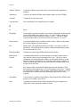
Figure 1-1 shows a comparison of MXIbus transfer data rates against those of RS-232 and GPIB.
>10 Mbytes/s
1 Mbytes/s
2 kbytes/s
RS-232
GPIB
PC AT
MXIbus
Micro Channel
EISAbus
NuBus
VXIbus
Figure 1-1. Comparison of Data Transfer Rates
VXI Connection
Many VXI users migrate from GPIB-based systems. As a result, a GPIB-to-VXI interface such
as the National Instruments GPIB-VXI is a popular way to control VXI instruments from a GPIB
controller. An increasingly popular way to control VXI, however, is to use a custom VXI
computer that plugs directly into the VXI mainframe. This embedded approach is technically
attractive because the computer communicates directly with the VXIbus and is tightly coupled to
the instruments.
An embedded computer is very powerful, but custom VXI computers cannot possibly keep pace
with the general-purpose computer market. In the last decade, specialized instrument controllers
have rapidly declined. General-purpose PCs and workstations, with their vast array of software
and accessories, have revolutionized our industry. By using general-purpose computers, the
instrumentation industry directly benefits from the billions of dollars spent each year in the
general computer market.
For VXI to truly become the platform for the 90s, it must align itself with the powerful general
computer market. This will enable VXI to take advantage of the billions of dollars being spent
and bring this investment to bear on the needs of the instrumentation community. VXI must be
able to take full advantage of industry-standard PCs, such as the PC AT, PS/2, Macintosh, and
EISA computers, as well as workstations from Sun, DEC, IBM, and others. VXI also must have
a transparent mechanism for extending to multiple mainframes, and a way to accommodate
instruments that can not physically fit on a VXI module. MXIbus meets each of these needs.
AT-MXI User Manual
1-2
© National Instruments Corporation
Chapter 1
Introduction to MXIbus
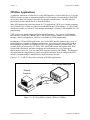
MXIbus Applications
A computer, instrument, or other device with a MXI interface is called a MXI device. Typically,
MXI devices are systems or instruments that have a MXI interface board installed. Most MXI
devices have their own internal system bus for internal communication. The MXI interface
board interfaces this internal bus to or from the MXIbus.
Many MXI products have been developed for VXI applications. MXI gives external computers
direct control of the VXIbus, as if they were embedded in the VXI mainframe. A VXI-to-MXI
mainframe extender can extend VXI to multiple mainframes. Software is also available for VXI
programming.
VME systems are another target application for MXI products. You can use VME interface
kits to directly control the VMEbus, and a VME-to-MXI chassis extender to extend VME for
multiple- chassis configurations. Software is available for VME programming.
In addition to VXI and VME applications, you can use MXI interface products in a variety of
general-purpose, computer-to-computer applications. You can mix and match MXI products
to interconnect any number of MXI devices for very high-performance communication. For
example, MXI can connect PC AT, EISA, PS/2, SunSPARCstation, DECstation 5000, RISC
System/6000, Macintosh, and other computers and workstations for a very high-speed,
shared-memory network. You can order MXI computer interfaces individually. The hardware
documentation has comprehensive register descriptions that show how to configure the MXI
interfaces programmably to establish such a shared-memory network.
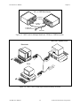
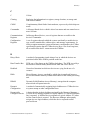
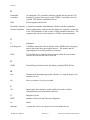
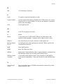
Figures 1-2, 1-3, and 1-4 show three examples of MXIbus applications.
VXI or VME Mainframe
External
Computer
es
I
VX fram
r
he ain
Ot M
To ME
V
or
ce
fa
ter
I In
MXI Cable
NA
INS TIO
TR
NA
UM L
EN
TS ®
bus
VXI-MXI or
VME-MXI
MX
Figure 1-2. PC Using MXI to Control VXIbus or VMEbus
© National Instruments Corporation
1-3
AT-MXI User Manual
Introduction to MXIbus
Chapter 1
VXI or VME Mainframes
L
NAENTS
TIO
UM
NATR
INS
bus
Embedded
Computer
®
NA
INS TIO
TR
NA
UM L
EN
TS ®
VXI-MXI or
VME-MXI
bus
To Other VXI
or VME Mainframes
MXI Cable
Figure 1-3. MXI Used for Multiple Mainframe VXIbus or VMEbus System
IBM RISC System 6000
Macintosh
XI
-M ce
B
N rfa
e
Int
XI
-M e
C
M rfac
e
Int
PS/2
r
he d
Ot ippe
o
u
T q
rs
I-e ute
MXomp
C
XI
-M e
C
a
M rf c
e
Int
Figure 1-4. MXI Used for High-Speed Shared-Memory Network
AT-MXI User Manual
1-4
© National Instruments Corporation
Chapter 1
Introduction to MXIbus
MXIbus – An Open Standard
Because MXI is an open industry standard, documented with a comprehensive specification, you
can design MXI interfaces for your own devices. In this way, your proprietary peripherals or
instruments can use MXI to connect to industry-standard computers or to a VXI or VME system.
Several third-party companies have successfully used the MXI specification to develop their own
MXI interfaces. National Instruments distributes the MXI specification, and will be pursuing
formal MXI standardization.
MXIbus Operation
MXIbus is a general-purpose, 32-bit, multimaster system bus on a cable. MXI interconnects
multiple devices with flexible, round cables similar to GPIB, but uses a hardware memorymapped communication scheme that eliminates all software overhead. MXI is very similar to
the VMEbus itself, and can be described as a backplane bus on a cable. You can daisy-chain
up to eight MXI devices together.
MXIbus tightly couples multiple devices by mapping together portions of their individual
address spaces. In other words, MXI devices connect at the hardware level, and operate as if
they are a single system with a shared address space. MXI devices can directly access each
other’s resources by performing simple reads and writes to appropriate address locations, thus
requiring no software protocol.
Each MXIbus hardware interface has address window circuitry that detects internal bus cycles
that map out to the MXIbus. Likewise, the circuitry also detects external MXIbus cycles whose
address maps into the system. When a hardware write or read occurs with an address that maps
across MXI, the MXI hardware interlocks the bus cycle between the devices across the MXIbus.
This hardware scheme matches the system used by embedded VXI computers to access VXI.
MXIbus Signals
The MXI connector is a single, rugged, high-density, 62-pin D-subminiature connector. MXIbus
signals include 32 multiplexed address and data lines with parity, address modifiers for multiple
address spaces, single-level multimaster prioritized bus arbitration, a single interrupt line, a bus
error line for handling timeouts and deadlock conditions, and handshake lines for asynchronous
operation. You can perform data transfers of 8, 16, and 32 bits, as well as indivisible read/write
operations and integrated block-mode transfers. The maximum data rate for MXIbus is 20
Mbytes/s.
MXIbus Cables
There are two basic types of MXIbus cables. One type of MXIbus cable is a point-to-point cable
with a single connector on each end. The other type of MXIbus cable is known as a multi-drop
cable, and has a single connector on one cable end and a double connector on the other end. A
MXIbus system consists of two or more MXIbus devices connected in a daisy-chain fashion.
Every MXIbus system has one MXI device that acts as the MXIbus System Controller. The
MXIbus System Controller must be the first device in the daisy-chain (requiring it to have a
single connector cable end). Subsequent devices will have the double connector end.
© National Instruments Corporation
1-5
AT-MXI User Manual
Introduction to MXIbus
Chapter 1
Figure 1-5 is a diagram of the multi-drop type of cable assembly used in a daisy-chained MXIbus
system. You can daisy-chain additional devices to the double connector to propagate the bus.
Use a MXIbus cable with a single connector on each end when the system contains only two
MXI devices or when you are connecting the last cable section in the daisy-chain.
Male (plug)
62-pin Connector
Piggy-Back
Connector Hood
This end attaches to the
device that is closer in
the daisy-chain to the
MXIbus System Controller
P2
P1
P3
Female (receptacle)
62-pin Connector
MXIbus Cable
Figure 1-5. MXIbus Multi-Drop Cable Assembly
A single MXI cable can be any length up to 20 m. If multiple MXI devices are daisy-chained
together, the total cable distance must be no more than 20 m. The MXI cable is a flexible, round
cable similar to a GPIB cable (about 0.6 in. in diameter). Internally there are 48 single-ended,
twisted-pair signal lines. Double shielding with an aluminum mylar shield as well as a copper
braid shield eliminates any EMI problems. The stacking depth of two daisy-chained MXI cables
is approximately 3.4 in.
MXI is essentially a backplane bus on a cable. Each MXI signal line is twisted with its own
ground line. All MXIbus signal lines have matched impedance to minimize signal skew and
reflections. Limiting stub lengths to no more than 4 in. off the mainline interconnection
minimizes reflections due to impedance discontinuities. You must have termination networks at
the first and last MXIbus devices to minimize reflections at the ends of cables.
MXI uses state-of-the-art, single-ended, trapezoidal bus transceivers to reduce noise crosstalk in
the transmission system. Designed specifically for driving backplane bus signals, these
transceivers have open-collector drivers that generate precise trapezoidal waveforms with typical
rise and fall times of 9 ns. The trapezoidal shape, due to the constant rise and fall times, reduces
noise coupling (crosstalk) on adjacent lines. The receiver uses a lowpass filter to remove noise
and a high-speed comparator that recognizes the trapezoidal-shaped signal from the noise.
AT-MXI User Manual
1-6
© National Instruments Corporation
Chapter 1
Introduction to MXIbus
MXIbus Termination
The MXIbus requires that the first and last devices in the daisy-chain have a termination
network. Two basic types of termination networks are available. Some MXIbus devices have
onboard termination schemes that should be enabled on the end devices of the daisy-chain. You
can also use external terminating packs for easy system reconfiguration and for MXIbus devices
that lack onboard terminating networks. MXIbus devices other than the two end devices should
not have an external terminating pack and must have any onboard terminating networks defeated.
Also, each end device must have only one of these termination options.
MXIbus Performance
It is often difficult to understand how a performance specification for a single component relates
to the overall performance of your system. In the case of MXI, it is important to understand not
only the performance issues associated with the MXI link, but also the devices that communicate
across the link. MXI works exactly like an embedded computer, using a direct hardware
memory-map to eliminate software overhead between your computer and the VXIbus or
VMEbus. Both MXI and embedded VXI computers can use shared memory communication
protocols and direct register accesses for potentially dramatic performance improvements over
GPIB. If your VXI instruments themselves do not use these capabilities, however, your system
performance using MXI or an embedded computer may be no higher than a GPIB-controlled
VXI system.
There are several factors to consider when comparing a MXI-equipped computer to an embedded
computer. A MXI-equipped computer is functionally equivalent to an embedded computer. In
fact, application software developed on a MXI computer can execute on an embedded computer
and vice versa. There are subtle hardware timing differences, but there is no dramatic
performance difference because of architecture. MXI, for example, can take approximately 100
ns more to perform a single VXI read or write than an embedded computer, because the MXI
signals must propagate down the MXI cable at 10 ns/m, and the signals must be synchronized by
each device involved in the transfer. This is negligible compared to the other factors that affect
your system performance, such as the execution speed of your application software or your
instruments.
Often, the most important performance issue to consider when evaluating a computer for your
system is the performance of the processor itself. Most applications spend much more time
computing, displaying, or performing disk I/O than actually performing I/O across the VXIbus or
VMEbus. Current external MXI computers are over four times as fast as the fastest embedded
VXI computer. In addition, because of the physical space constraints of embedded computers,
external computers often have much more sophisticated architectures with faster processors,
cache RAM, faster disk drives, and other benefits. Raw computing power can be the single most
important consideration for the performance of your system.
© National Instruments Corporation
1-7
AT-MXI User Manual
Introduction to MXIbus
Chapter 1
Data Transfer Rates
A common benchmark for VXI computers is the Block Data Rate. This benchmark is easy for
vendors to isolate and measure under ideal conditions. It is important to understand what Block
Data Rate means to your application. Block Data Rate is the rate at which you can move a large
block of data to or from memory on an ideal VXI device using back-to-back VXI transfers. It
does not measure how fast the computer can process the blocks of data or store them to disk once
they are moved, or whether your instruments themselves can actually support that data rate.
Most applications are not limited by the Block Data Rate of the VXI interface hardware, but
rather by the total time required to both move and handle the data, or by the rate at which the
instruments themselves can generate or accept the data.
Block Data Rate is easy for vendors to specify, but often difficult for users to relate to overall
system performance. It is only one of many elements that affect the actual throughput of your
system. For example, Block Data Rate does not indicate the processing power of your computer
or the performance of the instruments themselves. In addition, a benchmark for Block Data Rate
does not measure how fast you can control instruments using VXI Word Serial Protocol or
random VXI reads and writes. The speed for Word Serial communication and random VXI reads
and writes is dependent on the speed of the processor and the particular VXI instruments.
MXIbus Data Rates
The theoretical maximum Block Data Rate for MXI is 20 Mbytes/s. As with any bus, the
performance of a particular MXI interface depends on the actual design implementation for that
interface. All National Instruments MXI user manuals contain a Specifications appendix, in
which you will find both the single (random access) and block transfer rates for their respective
devices. You can think of these values as a propagation delay and use them to calculate the
transfer time of your system. To determine the MXI cycle time, add the appropriate master
rating of the device that will initiate the MXI transfer to the appropriate slave rating of the device
that will accept the MXI transfer.
The read/write access time of your remote system and the length of your MXI cable affect the
actual data transfer rate you can achieve. To determine the actual data transfer data rate to expect
with a particular device, consider the following equation:
Data Rate (bytes/s) =
Transfer Width (bytes)
Transfer Time (s)
where Transfer Width equals the number of bytes per transfer, and the Transfer Time equals the
sum of five components:
•
•
•
•
•
MXI Master Mode time
MXI Slave Mode time
Bus access time of the remote system
Recovery time of the local system (the time it takes the system to generate the next cycle
from an acknowledgement of the previous cycle)
MXI cable propagation time
The MXI cable propagation time is 10 ns/m.
AT-MXI User Manual
1-8
© National Instruments Corporation
Chapter 1
Introduction to MXIbus
For example, consider the National Instruments VXI-AT2000 kit. The MXI Master Mode time
of the AT-MXI is 190 ns for block reads and the MXI Slave Mode time of the VXI-MXI is 240
ns for block reads. Therefore, if your actual application uses a 2 m MXI cable (20 ns MXI cable
propagation time) and your VXI device has a bus access time of 100 ns, then the total transfer
time for a single read during a block is 550 ns (assuming a 0 ns recovery time for the local
system).
Note:
The following calculations assume a 0 ns recovery time. Thus, the block data rate
computed below is the theoretical maximum. Once you determine your system
recovery time, use that value with these calculations to determine the actual block
data rate for your system.
Assuming that your VXI device is a 16-bit (2 bytes/transfer) device, your expected Block Read
Data Rate to that VXI device using the VXI-AT2000 is 3.64 Mbytes/s as calculated by the
following formula:
2 bytes/transfer
Block Data Rate = 550 ns/transfer = 3.64 Mbytes/s
Local Performance
The MXIbus does not degrade the performance of the devices connected to it. Each MXI device
can operate internally at full speed in parallel with other MXI devices. Because MXIbus is a true
system bus with multimaster arbitration, the only time MXI devices must synchronize their
operation is when they perform transactions that map across the MXIbus. When one MXI device
performs a read or write that maps to a remote MXI device, the MXI hardware on both devices
interlocks the bus cycle across the MXIbus to accomplish the transfer.
© National Instruments Corporation
1-9
AT-MXI User Manual
Chapter 2
General Information
This chapter contains an overview of the functionality of the AT-MXI interface board, shows a
picture of the AT-MXI board, and lists the contents of your kit and available optional equipment.
The AT-MXI is an interface board that links an IBM Personal Computer AT or compatible
computer (hereafter referred to as the PC AT) directly to the MXIbus. It uses address mapping to
translate bus cycles on the PC AT bus to the MXIbus and vice versa. Figure 2-1 shows the
AT-MXI interface board.
Figure 2-1. AT-MXI Interface Board
Overview
The AT-MXI can function as both a MXIbus master and a MXIbus slave. When operating as a
MXIbus master, the AT-MXI converts PC AT memory cycles initiated by the CPU or an
alternate bus master on the PC AT bus into MXIbus cycles intended for a MXIbus slave device.
When operating as a MXIbus slave, the AT-MXI converts MXIbus cycles initiated by a MXIbus
master into PC AT memory or I/O bus cycles so that other MXIbus devices can freely access
(share) resources within the PC AT.
As a MXIbus master, the AT-MXI supports 32-bit (A32), 24-bit (A24) and 16-bit (A16)
addressing. As a MXIbus slave, the AT-MXI supports A24 addressing to PC AT memory and
A16 addressing to the AT-MXI communication registers and to the PC AT I/O space. The
AT-MXI supports both 16-bit (D16) and 8-bit (D08) data transfers while operating as either a
MXIbus master or a MXIbus slave. The AT-MXI cannot support 32-bit (D32) data transfers
because the PC AT data bus is only 16 bits wide.
© National Instruments Corporation
2-1
AT-MXI User Manual
General Information
Chapter 2
Because the AT-MXI uses the same communication register set that is used by VXIbus MessageBased devices, other MXIbus devices can view the AT-MXI as a VXIbus device. The following
are some of the numerous benefits that can result from using the VXIbus register architecture:
•
•
•
•
•
Dynamic device identification and configuration during system initialization
Standardized Word Serial communication between devices
Dynamic resource (memory) allocation
Message (signal) passing protocols between devices
Shared memory architectures
The AT-MXI supports MXIbus block-mode transfers while operating as either a MXIbus master
or a MXIbus slave. With block-mode transfers, data located in consecutive memory locations
can be transferred at higher rates because MXIbus addressing information is not sent with each
data transfer. The AT-MXI supports the use of the direct memory access (DMA) controller on
the PC AT computer when transferring block-mode data between the PC AT bus and the
MXIbus. Optionally, any MXIbus or PC AT bus master can be used to initiate and transfer
block-mode data via the AT-MXI.
In addition to these features, the AT-MXI is also able to function as the MXIbus System
Controller and can terminate the MXIbus signals directly on the AT-MXI interface board. The
AT-MXI also supports the MXIbus arbitration lock and fairness options.
What Your Kit Should Contain
Your AT-MXI kit should contain the following components:
Kit Component
Part Number
AT-MXI Interface Board
180775-01
AT-MXI User Manual
320339-01
AT-MXI User Manual
2-2
© National Instruments Corporation
Chapter 2
General Information
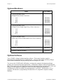
Optional Hardware
Cables
Part Number
Type M1 MXIbus Cables
Straight Point-to-Point Connectors:
– 1m
– 2m
– 4m
– 8m
– 20 m
180758-01
180758-02
180758-04
180758-08
180758-20
Type M2 MXIbus Cables
Straight Point-to-Right Angle Daisy-Chain Connectors:
– 1m
– 2m
– 4m
– 8m
– 20 m
180760-01
180760-02
180760-04
180760-08
180760-20
Type M3 MXIbus Cables
Right Angle Point-to-Right Angle Daisy-Chain Connectors:
– 1m
– 2m
– 4m
– 8m
– 20 m
180761-01
180761-02
180761-04
180761-08
180761-20
MXIbus Terminating Pac (External)
180780-01
MXIbus Connector Extender
181663-01
Optional Software
Your AT-MXI is shipped without interface software. This manual contains complete
instructions for programming the AT-MXI directly. You can order various software packages
from National Instruments for programming and controlling the AT-MXI.
You can use the AT-MXI with LabWindows, an innovative program development software
package for test and measurement applications. LabWindows enhances Microsoft QuickBASIC
and C with an interactive development environment, function panels to generate source code, and
libraries for data acquisition, instrument control, and data analysis and presentation.
LabWindows for DOS is available for programming in C or BASIC. LabWindows/CVI is a
complete, full-function C programming environment for PC-compatible computers running
Windows.
© National Instruments Corporation
2-3
AT-MXI User Manual
General Information
Chapter 2
You can also use the AT-MXI with LabVIEW, a complete programming environment with a
unique graphical methodology. LabVIEW departs from the sequential nature of traditional
programming languages and features a graphical programming environment and all the tools
needed for data acquisition, analysis, and presentation. LabVIEW matches the modular virtual
instrument capability of VXI, and can reduce your VXIbus software development time.
LabVIEW packages are available for PC-compatible computers running either Windows or
Windows NT.
The AT-MXI can also be used with the NI-VXI bus interface software package, a comprehensive
software package for configuring, programming, and truobleshooting a VXI system. NI-VXI
features a standardized set of utilities and C library functions that give you simple, low-level
access to other MXIbus devices. NI-VXI is available across many different operating system
platforms.
The following table lists the application software packages and the NI-VXI bus interface
software packages you can order for the AT-MXI.
Software
Part Number
LabWindows VXI Development System for DOS
LabWindows/CVI VXI Development System for Windows
LabVIEW VXI Development System for Windows
LabVIEW VXI Development System for Windows NT
776729-01
776804-01
776674-01
776774-01
NI-VXI Bus Interface Software Packages for AT-MXI
–
–
–
–
–
MS-DOS
Microsoft Windows
SCO UNIX
ISC UNIX
Windows NT
AT-MXI User Manual
776418-01
776458-01
776368-02
776368-03
776873-58
2-4
© National Instruments Corporation
Chapter 3
Configuration and Installation
This chapter describes the procedures for unpacking, configuring, and installing your AT-MXI
interface board. The instructions are given in the order that you should perform them. A
summary of the steps is as follows:
1.
2.
3.
4.
Unpack the AT-MXI.
Configure the AT-MXI.
Install the AT-MXI.
Connect the AT-MXI to the rest of your MXIbus system.
Step 1. Unpack the AT-MXI
Follow these steps when unpacking your AT-MXI interface board:
1. Before attempting to configure or install the AT-MXI, inspect the shipping container and its
contents for damage. If damage appears to have been caused in shipment, file a claim with
the carrier. Retain the packing material for possible inspection and/or for reshipment.
2. Verify that the pieces contained in the package you received match the kit parts list. Do not
remove the board from its plastic bag at this point.
3. Your AT-MXI board is shipped packaged in an antistatic plastic bag to prevent electrostatic
damage to the board. Some of the circuitry on the AT-MXI uses CMOS technology and can
be damaged by electrostatic discharge. Before removing the board from the antistatic bag,
touch the bag to a metal part of your computer chassis.
4. As you remove the AT-MXI from its bag, be sure to handle the board only by its edges.
Avoid touching any of the IC components or connectors. Inspect the board for loose
components or any other sign of damage. Notify National Instruments if the board appears
damaged in any way. Do not install equipment that appears to be damaged.
Step 2. Configure the AT-MXI
You can configure four options on the AT-MXI board:
•
•
•
•
Base I/O address
Interrupt levels
DMA channels
MXIbus termination option
© National Instruments Corporation
3-1
AT-MXI User Manual
Configuration and Installation
Chapter 3
Figure 3-1 shows the location of the AT-MXI configuration jumpers, switches and terminator
sockets.
Figure 3-1. AT-MXI Parts Locator Diagram
AT-MXI User Manual
3-2
© National Instruments Corporation
Chapter 3
Configuration and Installation
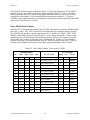
Switch and Jumper Settings
Table 3-1 shows the factory settings and optional settings for the configurable options on the
AT-MXI.
Table 3-1. AT-MXI Factory Default Settings and Optional Configurations
Feature
Default
Optional Configurations
340
100 to 3E0, increments of 20 hex
Board Interrupt Level
12
3, 4, 5, 6, 7, 9, 10, 11, 12, 14, 15,
and Not Used
MXIbus Interrupt Level
10
3, 4, 5, 6, 7, 9, 10, 11, 12, 14, 15,
and Not Used
Base I/O Address (hex)
Master DMA Channel
6
0, 1, 2, 3, 5, 6, 7, and Not Used
Slave DMA Channel
3
0, 1, 2, 3, 5, 6, 7, and Not Used
MXIbus Termination
Installed
Not Installed
The factory-configured settings of the base I/O address, the interrupt levels, and the DMA
channels are suitable for most computer systems. The following sections describe under what
conditions it would be necessary to change the configuration jumpers, switches, and/or
terminators on the AT-MXI and how to make these changes.
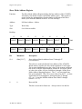
Base I/O Address Selection
The base I/O address of the AT-MXI is the starting address of the AT-MXI configuration
registers in PC AT I/O space. The base I/O address is determined by the position of the five
switches at location U31, as shown in Figure 3-1. The switches are set at the factory for a base
I/O address of 340 hex. Because the AT-MXI requires 32 bytes of consecutive I/O space for its
internal registers, the factory configuration uses the I/O address space in the range of 340 to 35F
hex.
Note:
Check to determine that this I/O space is not already used by any other interface
installed in your PC AT computer. If any equipment in your computer uses this I/O
address space, you must change either the base I/O address of the AT-MXI or the I/O
address space requirements of the other device. All PC AT devices must have a
unique partition of the system's I/O address space.
Each switch in U31 (1 through 5) corresponds to one of the PC AT address lines (A5 through
A9). The first switch (1) corresponds to address line A5, the next switch (2) corresponds to
address line A6, and so on. The five least significant bits of the address (A4 through A0) are
used by the AT-MXI to select the appropriate AT-MXI register and cannot be changed;
therefore, bits A4 through A0 are always zeros when determining the base I/O address.
© National Instruments Corporation
3-3
AT-MXI User Manual
Configuration and Installation
Chapter 3
To change the base I/O address of the AT-MXI, press the side marked OFF to select a binary
value of 1 for the corresponding address bit. Press the ON side of the switch to select a binary
value of 0 for the corresponding address bit. Refer to Table 3-2.
Figure 3-2 shows two possible switch settings.
U31
1
OFF
2
3
4
5
Binary Hex
0
0 0
0
0
0
ON=0
0
ON=0
ON=0
OFF=1
ON=0 1
a. Switch Set to Base I/O Address hex 100
U31
1
OFF
2
3
4
5
Binary Hex
0
0 0
0
0
0
ON=0
OFF=1 4
ON=0
OFF=1
OFF=1 3
b. Switch Set to Default Setting
(Base I/O Address hex 340)
Figure 3-2. Base I/O Address Switch Settings
AT-MXI User Manual
3-4
© National Instruments Corporation
Chapter 3
Configuration and Installation
Table 3-2 lists the 24 possible switch settings, the corresponding base I/O address, and the I/O
address space used for that setting. Notice that the base address settings that correspond to an
I/O address in the range from 0 to FF hex are not listed. These addresses are used by logic on the
PC AT motherboard and cannot be used by I/O adapter modules.
Table 3-2. Possible Base I/O Address Settings for the AT-MXI
Switch Setting
A9 A8 A7 A6 A5
Base I/O Address
(hex)
I/O Ports Used
(hex)
0 1
0
0
0
100
100 - 11F
0 1
0
0
1
120
120 - 13F
0 1
0
1
0
140
140 - 15F
0 1
0
1
1
160
160 - 17F
0 1
1
0
0
180
180 - 19F
0 1
1
0
1
1A0
1A0 - 1BF
0 1
1
1
0
1C0
1C0 - 1DF
0 1
1
1
1
1E0
1E0 - 1FF
1 0
0
0
0
200
200 - 21F
1 0
0
0
1
220
220 - 23F
1 0
0
1
0
240
240 - 25F
1 0
0
1
1
260
260 - 27F
1 0
1
0
0
280
280 - 29F
1 0
1
0
1
2A0
2A0 - 2BF
1 0
1
1
0
2C0
2C0 - 2DF
1 0
1
1
1
2E0
2E0 - 2FF
1 1
0
0
0
300
300 - 31F
1 1
0
0
1
320
320 - 33F
1 1
0
1
0
340 (default)
340 - 35F
(continues)
© National Instruments Corporation
3-5
AT-MXI User Manual
Configuration and Installation
Chapter 3
Table 3-2. Possible Base I/O Address Settings for the AT-MXI (Continued)
Switch Setting
A9 A8 A7 A6 A5
Base I/O Address
(hex)
I/O Ports Used
(hex)
1 1
0
1
1
360
360 - 37F
1 1
1
0
0
380
380 - 39F
1 1
1
0
1
3A0
3A0 - 3BF
1 1
1
1
0
3C0
3C0 - 3DF
1 1
1
1
1
3E0
3E0 - 3FF
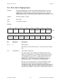
Interrupt Level Selection
The AT-MXI interface board can use one, two, or none of the eleven interrupt levels of the PC
AT I/O bus. Setting up an interrupt level for operation involves two steps. First you select the
interrupt level by arranging the jumpers on an array of pins. Next you enable the interrupt level
in the system software. Interrupt levels must be enabled by the system software before they can
function. Any interrupt level not enabled is not driven by the AT-MXI and can be used by other
devices, regardless of the positions of the jumpers.
Interrupt levels are selected by the position of two jumpers on the 3 by 11 array of pins labeled
W3, located above the I/O card-edge connector on the AT-MXI (refer to Figure 3-1). The
jumper farther from the card-edge connector is used to select which PC AT interrupt level is used
to convey board status and error information. This jumper is set at the factory to a default level
of 12.
The jumper on the W3 pin array closer to the I/O card-edge connector is used to select which PC
AT interrupt level corresponds to the MXIbus interrupt signal IRQ*. Because the MXIbus
interrupt is also one of the conditions covered by the other jumper, a separate interrupt level for
the MXIbus IRQ* signal is normally not needed and is useful only if you want a different
interrupt vector or priority for MXIbus interrupts. This jumper is set at the factory to a default
level of 10.
Note:
The AT-MXI does not have the ability to share interrupt levels with other devices. If
you select an interrupt level by placing a jumper on a particular level and enable that
level in software, no other device in the system can use that level. Make sure that no
other devices in your system use the interrupt level(s) selected and enabled for use by
the AT-MXI. If they do, change the interrupt level(s) of either the AT-MXI or the
other devices.
The AT-MXI can use interrupt levels IRQ3, 4, 5, 6, 7, 9, 10, 11, 12, 14, and 15. Be careful when
re-assigning interrupt levels on the AT-MXI. Notice that most PC ATs use interrupt level 6 for
the diskette drive controller and interrupt level 14 for the hard disk drive controller. Other
interrupt levels might be used by standard logic devices on the motherboard, so check your
computer documentation before changing interrupt levels on the AT-MXI.
AT-MXI User Manual
3-6
© National Instruments Corporation
Chapter 3
Configuration and Installation
Once you have chosen an interrupt level, place the jumper on the appropriate pins to select that
interrupt level. Use the two rows of pins farther from the card-edge connector to select the board
interrupt level, and the two rows of pins closer to the card-edge connector to select the MXIbus
interrupt level. Figure 3-3a shows the factory default interrupt jumper setting of the AT-MXI,
with board interrupt level 12 and MXIbus interrupt level 10.
•
•
•
•
•
•
•
•
•
•
•
•
•
•
•
•
•
•
•
•
•
•
•
•
IRQ3
•
IRQ4
•
•
IRQ5
•
•
IRQ6
•
•
IRQ7
•
•
IRQ9
•
•
IRQ10
•
•
IRQ11
To set Board
Interrupt Level
•
•
IRQ12
•
•
•
IRQ14
•
•
•
•
•
IRQ3
•
IRQ4
IRQ15
•
•
•
•
•
•
•
•
•
IRQ5
•
IRQ6
•
IRQ7
•
IRQ9
To set MXIbus
Interrupt Level
To set Board
Interrupt Level
•
IRQ10
•
IRQ11
•
IRQ12
•
IRQ14
•
IRQ15
•
To set MXIbus
Interrupt Level
W3
W3
a. Factory Default
Interrupt
Jumper Setting–
Board Interrupt Level 12,
MXIbus Interrupt Level 10
b. Board Interrupt Level 5,
MXIbus Interrupt Level 10
Figure 3-3. Board and MXIbus Interrupt Jumper Settings
To change to another interrupt level, remove the appropriate jumper from its current position and
place it on the new posts. Figure 3-3b shows the board interrupt level changed to IRQ5.
© National Instruments Corporation
3-7
AT-MXI User Manual
Configuration and Installation
Chapter 3
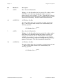
DMA Channel Selection
The AT-MXI interface board can use one, two, or none of the seven DMA channels of the PC
AT I/O bus. Setting up a DMA channel for operation involves two steps. First you select the
DMA channel by arranging the jumpers on an array of pins. Next you enable the DMA channel
in the system software. DMA channels must be enabled by the system software before they can
function. Any DMA channel not enabled is not driven by the AT-MXI and can be used by other
devices, regardless of the positions of the jumpers.
Select the DMA channels on the two 3 by 7 arrays of pins labeled W1 and W2, located above the
I/O card-edge connector on the AT-MXI (refer to Figure 3-1). Use the W1 array to select the
DMA request line(s), and use the W2 array to select the DMA acknowledge line(s). You must
position two jumpers to select a single DMA channel. The DMA ACKnowledge (DACKn) and
DMA ReQuest (DRQn) lines selected must have the same numeric suffix for proper operation.
Therefore, make sure that the jumper positions on the W1 array are identical to the jumper
positions on the W2 array.
Master Mode Versus Slave Mode
The AT-MXI can function as both a MXIbus master and a MXIbus slave. As a MXIbus master,
the AT-MXI circuitry determines whether a PC AT cycle is to be mapped into a MXIbus cycle
intended for some external MXIbus device, such as a VMEbus chassis. As a MXIbus slave, the
AT-MXI circuitry determines whether an external device is attempting to access PC AT memory
or I/O resources. When allocating DMA channels for use by the AT-MXI, keep in mind that
master-mode and slave-mode operation are two distinct asynchronous functions and require
different DMA channels.
The slave-mode DMA channel must be enabled to allow shared access to PC AT resources from
an external MXIbus master. If you intend to share memory or I/O resources within the PC AT,
you must select and enable a DMA channel for slave-mode operation.
You can use the master-mode DMA channel to perform high-speed block-mode transfers to or
from external MXIbus devices. If you selected a master-mode DMA channel and enabled it in
software, all block-mode transfers that map to the MXIbus will use the PC AT DMA controller
to perform the block-mode move via that channel.
If the master-mode DMA channel is not enabled by software, the jumper-selected DMA channel
is not used by the AT-MXI and can be used by other devices. Block-mode transfers can still be
performed by using the processor's movs (move string) command or by writing a move string
function. This does not necessarily mean that it will take any longer for the data to be
transferred. In fact, most PC ATs can transfer data faster using the movs instruction than they
can using the DMA controller. However, you may prefer to use the DMA controller if you have
other useful work to do during a block-mode operation (such as when using a multitasking
operating system).
AT-MXI User Manual
3-8
© National Instruments Corporation
Chapter 3
Configuration and Installation
The DMA jumpers are configured at the factory set to master-mode DMA Channel 6 and slavemode DMA Channel 3.
Note:
Seldom, if ever, can the AT-MXI share DMA channels with other devices. If you
have selected a DMA channel by placing jumpers on that channel's request and
acknowledge lines and enabled the channel in software, no other devices in your
system should use that channel. If DMA channels conflict, change the DMA
channel(s) used by either the AT-MXI or the other device(s).
The AT-MXI can use DMA Channels 0, 1, 2, 3, 5, 6, and 7. Be careful when re-assigning DMA
channels on the AT-MXI. Notice that most PC ATs use DMA Channel 2 for the disk controller
interface. Other DMA channels might be used by standard logic devices on the motherboard, so
check your computer documentation before changing DMA channels.
Notice that the PC AT makes a distinction between 8-bit and 16-bit DMA channels. The 8-bit
channels are 0, 1, 2, and 3. The 16-bit channels are 5, 6, and 7. The master-mode DMA channel
must be set on a level that matches the data width of the intended block transfers. It is preferable
to use one of the 16-bit channels for the master-mode interface because a 16-bit DMA channel
can transfer twice the amount of data in the same number of cycles. The slave-mode DMA
channel is used only to request the PC AT bus for an alternate PC AT bus master cycle. It can
use any available 8-bit or 16-bit channel regardless of the intended data width of the transfers.
Use the two rows of pins farther from the card-edge connector to select the master-mode DMA
channel and the two rows closer to the card-edge connector to select the slave-mode DMA
channel. Remember that the jumper positions should be identical on both the W1 and W2 arrays.
Figure 3-4a shows the factory default DMA channel setting of the AT-MXI, with master-mode
DMA Channel 6 and slave-mode DMA Channel 3.
© National Instruments Corporation
3-9
AT-MXI User Manual
Configuration and Installation
Chapter 3
•
•
•
•
•
•
•
•
•
•
•
•
•
•
•
•
•
•
•
•
•
•
•
•
•
•
•
•
DACK0
•
DACK1
•
•
DACK2
•
•
DACK3
•
•
DACK5
•
•
•
DACK6
•
•
•
•
•
•
•
•
•
•
DACK7
•
DACK0
•
DACK1
•
DACK2
•
DACK3
•
DACK5
•
DACK6
•
•
W1
W1
DACK7
•
•
DRQ0
•
DRQ1
•
•
DRQ2
•
•
DRQ3
•
•
DRQ5
•
•
•
DRQ6
•
•
•
•
•
•
•
•
•
•
•
DRQ7
•
DRQ0
•
DRQ1
•
DRQ2
•
DRQ3
•
DRQ5
Master
DRQ6
Slave
Master
Slave
DRQ7
W2
W2
a. Factory Default DMA
Channel Jumper Setting:
Master Mode Channel 6,
Slave Mode Channel 3
b. DMA Channel Jumper
Setting
for Master Mode Channel 7,
Slave Mode Channel 0
Figure 3-4. DMA Channel Settings
To change to another DMA channel, remove both the DRQ and DACK jumpers from their
current positions and place them on their new posts. Figure 3-4b displays the jumper position
necessary for selecting master-mode DMA Channel 7 and slave-mode DMA Channel 0.
MXIbus Termination Option
The AT-MXI has the ability to terminate the MXIbus signals on the interface board using
terminating resistor networks in single inline packages (SIPs). You also have the option of
terminating the MXIbus signals externally, by using an add-on module to aid in easy system
reconfiguration. As mentioned in Chapter 1, only the first and last devices in the MXIbus daisychain should be terminated.
AT-MXI User Manual
3-10
© National Instruments Corporation
Chapter 3
Configuration and Installation
Because of the onboard termination option, you can install or remove terminating resistor
networks from their sockets on the AT-MXI board. The board is shipped from the factory with
these terminating resistor networks installed. If your AT-MXI is to be the first or last device in
the MXIbus daisy-chain and you will not be using external terminating resistor networks, leave
these internal resistor terminators in place. If the AT-MXI is not going to be an end device on
the MXIbus daisy-chain, or if you will be using external terminating resistor networks, remove
all six of the internal terminating resistor networks from their sockets. Store them in a safe place
in case the MXIbus system configuration changes. When reinstalling the resistor networks, be
sure to note the position of pin 1 of the socket and the terminators and make sure that the
terminating networks are plugged firmly into their respective sockets.
Figure 3-5 shows the position of the six MXIbus terminating networks. All six networks must be
either installed or removed from their sockets.
Figure 3-5. MXIbus Terminating Networks
© National Instruments Corporation
3-11
AT-MXI User Manual
Configuration and Installation
Chapter 3
Step 3. Install the AT-MXI
In the space provided here, record the settings of the base I/O address, the DMA channel(s), the
interrupt level(s), and the position of the MXIbus termination option so that you will have them
handy for future reference.
AT-MXI
Setting
Base I/O Address
Board Interrupt Level
MXIbus Interrupt Level
Master DMA Channel
Slave DMA Channel
MXIbus Termination Option
Before attempting to install the AT-MXI, notice that some MXIbus cable connector hoods are
slightly wider than most standard connector hoods and might interfere with other cables installed
in adjacent PC AT slots. Normally, this will only be a problem if the cable connector hoods for
the adjacent slots are also oversized. When choosing a PC AT slot in which to install the
AT-MXI, verify that the MXIbus cable connector will not interfere with cables and connectors in
other PC AT slots. If necessary, reposition the boards in the system to prevent cabling conflicts.
It may also help to install the AT-MXI in one of the end slots so that you will only have to
contend with the cable connectors of one other board.
If you cannot configure the AT-MXI to co-exist in an existing PC AT system by repositioning
the boards, you can use one of the MXIbus cable options with a straight-point connector hood on
the cable end that attaches to the AT-MXI. The straight-point connector hood is narrower than
the MXIbus dual-connector arrangement and provides an easier fit for many system
configurations. However, this approach requires that the AT-MXI be the first device in the
MXIbus daisy-chain because a cable with a straight-point connector end cannot accept another
MXIbus cable to propagate the bus. Remember that the first device in the MXIbus daisy-chain
must also be configured as the MXIbus System Controller.
The following instructions are general installation instructions. Consult the user or technical
reference manual of your computer for specific instructions and warnings.
1. Plug in your PC AT computer before installing the AT-MXI. The plug grounds the computer
and protects it from electrical damage while you are installing boards.
Warning:
To protect both yourself and the computer from electrical hazards, the
computer should remain off until you are finished installing the board.
AT-MXI User Manual
3-12
© National Instruments Corporation
Chapter 3
Configuration and Installation
2. Remove the top cover or access port to the PC AT I/O bus.
3. Select any available 16-bit full-length PC AT expansion slot. The 16-bit expansion slots
have two card-edge receptacle connectors.
4. Locate the metal bracket that covers the cut-out in the back panel of the PC AT chassis for
the slot you have selected. Remove and save the bracket-retaining screw and the bracket
cover.
5. Before picking up the AT-MXI, touch the metal part of the power supply case inside the
computer to discharge any static electricity that might be on your clothes or body.
6. Line up the AT-MXI with the MXIbus connector near the cut-out on the back panel and the
other card edge lined up with the respective slot guide. Slowly push down on the front of the
AT-MXI until its card edge connector is resting on the expansion slot receptacle. Using
slow, evenly distributed pressure, press the AT-MXI straight down until it seats in the
expansion slot.
7. Reinstall the bracket retaining screw to secure the AT-MXI to the back panel rail.
8. Check the installation.
9. Replace the computer cover.
Step 4. Connect the AT-MXI to the MXIbus
After the AT-MXI has been installed, add it to the rest of your MXIbus system by connecting the
MXIbus cable(s) to the MXIbus connector on the back of the board and to the other MXIbus
devices in your system. The AT-MXI should be connected to the MXIbus system as described
in Chapter 1. Be sure to tighten the screw locks on both sides of the cable connectors to ensure
proper pin connection.
Once the AT-MXI is properly connected to the MXIbus system, you can restore power to the PC
AT computer. The AT-MXI will remain offline on the MXIbus until it is initialized by the
system software. Make sure that all devices on the MXIbus are powered up, initialized and
operational before attempting to transfer data on the MXIbus.
© National Instruments Corporation
3-13
AT-MXI User Manual
Chapter 4
Register Descriptions
This chapter contains detailed information on the use of the AT-MXI registers that are accessible
via the PC AT bus using I/O operations. These registers are used to configure and control the
board's operation and to obtain relevant status information on the state of the board and the
MXIbus.
Another group of AT-MXI registers are accessible via MXIbus A16 space after the board has
been properly configured. Refer to Chapter 5, Programming Considerations, for a description of
these registers.
Note:
If you plan to use the NI-VXI software package, you do not need to read this chapter
because the software routines automatically handle the configuration and
maintenance of these registers.
Register Map
The AT-MXI maps its registers into 32 consecutive byte-wide I/O locations starting at the I/O
address established by the onboard switches (see Chapter 3). Some of the registers are read-only,
while others are write-only registers. All register pairs can be accessed as either words or bytes
except for the Signal Register, which must be accessed as a word, and the timer registers, which
must be accessed as bytes. When a 16-bit register is accessed with a byte-wide operation, the
least significant 8 bits are available at the even I/O address, while the most significant 8 bits are
available at the odd I/O address.
The register map for the AT-MXI registers is shown in Table 4-1. The table gives the register
name, the register address, the type of the register (read or write), and the size of the register in
bits.
© National Instruments Corporation
4-1
AT-MXI User Manual
Register Descriptions
Chapter 4
Table 4-1. AT-MXI Register Map
Mnemonic
Offset from
Base Address
(hex)
Type
Size
(bits)
Slave Mode Configuration Register Group:
Slave Mode Address Register
Slave Mode Address Mapping Register
SMAR
SMAMR
00
02
Write
Write
16, 8
16, 8
Master Mode Configuration Register Group:
Master Mode Address Page Register
Master Mode Address Modifier and Enable
MMAPR
MMAMEN
04
06
Write
Write
16, 8
16, 8
Board Register Group:
Signal Register
Board Status Register
Board Control Register
SR
BSR
BCR
08
0A
0A
Read
Read
Write
16
16, 8
16, 8
Timer Register Group:
Slave Mode Timer Register
Master Mode Timer Register
System Controller Timer Register
Timer Control Register
SMTR
MMTR
SCTR
TCR
10
12
14
16
Write
Write
Write
Write
8
8
8
8
Register Name
Table 4-1 shows the AT-MXI registers divided into four different register groups. These groups
represent the four major logic blocks on the AT-MXI interface card. The Slave Mode
Configuration Register Group is used to configure the AT-MXI interface so that it can accept
MXIbus cycles intended for PC AT resources. The Master Mode Configuration Register Group
is used to configure and control the AT-MXI when it is operating as a MXIbus master. The
Board Register group consists of registers that are used to configure the different board options
and obtain relevant status information from the AT-MXI board. The Timer Register Group is
used to establish time limits for the different modes of operation of the AT-MXI. The following
pages contain bit descriptions of each of the registers making up these groups.
AT-MXI User Manual
4-2
© National Instruments Corporation
Chapter 4
Register Descriptions
Register Description Format
The remainder of this chapter discusses each of the AT-MXI registers in the order shown in
Table 4-1. The individual register descriptions give the function, address, type, size, and bit map
of the register, followed by a detailed description of each bit function.
Each register bit map shows a diagram of the register with most significant bit (bit 15 for a 16-bit
register, bit 7 for an 8-bit register) shown on the left, and the least significant bit (bit 8 or bit 0)
shown on the right. A square is used to represent each bit. Each bit is labeled with a name inside
its square. Odd to the right of the bit diagram indicates that the byte can be accessed at an odd
I/O address. Even indicates that the byte can be accessed at an even I/O address. An asterisk (*)
after the bit name indicates that the signal is active low (negative logic).
Any register or bit that is cleared by a PC AT hard reset is so noted in its description. When you
power-on the unit or depress the reset button on the PC AT, the PC AT RESET signal is asserted,
resulting in a hard reset. Unless otherwise specified, the bits within all write registers remain as
programmed until they are overwritten.
In the following register descriptions, setting a bit means to write a value of 1 and clearing a bit
means to write a value of 0.
© National Instruments Corporation
4-3
AT-MXI User Manual
Register Descriptions
Chapter 4
Slave Mode Address Register
Function:
The Slave Mode Address Register defines the base address of the AT-MXI's
A24 and/or A16 shared resources in MXIbus address space. This register is
used to define the starting address for the window(s) through which slavemode cycles from the MXIbus to the PC AT bus will map.
Address:
I/O Base Address + 00 hex
Type:
Write Only
Size:
8 or 16-bit accessible
Bit Map:
15
14
13
12
11
10
9
8
SMA23
SMA22
SMA21
SMA20
SMA19
SMA18
SMA17
0
7
6
5
4
3
2
1
0
SMA15
SMA14
SMA13
SMA12
SMA11
SMA10
SMA9
0
Bit
Mnemonic
Description
15-9
SMA[23-17]
Slave Address Bits for Address Lines 23 through 17
(A24 accesses)
Odd
Even
These bits are used to define the base address of the AT-MXI's
shared memory window for slave-mode operation via A24 space.
The m most significant bits are the values of the m most significant
bits of the AT-MXI's shared address window in A24 space, where
m is the value of the A24 size field (bits 6 through 4 of the Slave
Mode Address Mapping Register). The (7 - m) least significant
bits are meaningless. Thus, for a given value of m, the (7 - m) least
significant bits are meaningless, and register bits 15 through
(15 - m + 1) map the MXIbus address lines SMA23 through
(SMA23 - m + 1).
8
0
Reserved Bit
This bit is reserved for future use. Always write a 0 to this bit.
AT-MXI User Manual
4-4
© National Instruments Corporation
Chapter 4
Register Descriptions
Bit
Mnemonic
Description
7-1
SMA[15-9]
Slave Address Bits for Address Lines 15 through 9
(A16 accesses)
These bits are used to define the base address of the AT-MXI's
shared memory window for slave-mode operation via A16 space.
The n most significant bits are the values of the n most significant
bits of the AT-MXI's shared address window in A16 space, where
n is the value of the A16 size field (bits 2 through 0 of the Slave
Mode Address Mapping Register). For a given value of n, the
(7 - n) least significant bits are meaningless, and register bits 7
through (7 - n + 1) map the MXIbus address lines SMA15 through
(SMA15 - n + 1).
Because the AT-MXI has fixed configuration registers located in
the top quarter of A16 space, this space is considered reserved.
You should not use this space when mapping MXIbus A16 space
to the PC AT bus. Confine the base address programmed in this
register to the lower 48 KB of A16 space (never set both bits 7 and
6 at the same time).
0
0
Reserved Bit
This bit is reserved for future use. Always write a 0 to this bit.
© National Instruments Corporation
4-5
AT-MXI User Manual
Register Descriptions
Chapter 4
Slave Mode Address Mapping Register
Function:
The least significant byte of the Slave Mode Mapping Register is used to
enable the AT-MXI slave-mode windows and to set their size. The most
significant byte of this register can be used to remap the A24 window in
MXIbus address space to a different physical address space on the PC AT bus.
Address:
I/O Base Address + 02 hex
Type:
Write Only
Size:
8 or 16-bit accessible
Bit Map:
15
14
13
12
0
0
0
0
7
6
5
4
A24EN
A24SIZ2 A24SIZ1 A24SIZ0
Bit
Mnemonic
Description
15-12
0
Reserved Bits
11
10
9
8
A24OFF3 A24OFF2 A24OFF1 A24OFF0
3
A16EN
2
1
Odd
0
A16SIZ2 A16SIZ1 A16SIZ0
Even
These bits are reserved for future use. Always write a 0 to these
bits.
11-8
A24OFF[3-0]
A24 Window Offset Bits
The value of these bits is added to the MXIbus address lines
AD[23-20] to form the PC AT address used during slave-mode
A24 accesses to PC AT memory. This register can be used to
remap MXIbus address space to a different physical PC AT
address space. The 4-bit resolution of this register makes it
possible to remap PC AT memory on 1 MB boundaries.
Because any carry generated as a result of the addition will be
discarded, the value of these bits should be considered a 2's
complement number when determining the mapping function. PC
AT addresses can therefore be at either a higher or lower address
than that of the MXIbus. These bits are cleared after a hard reset.
AT-MXI User Manual
4-6
© National Instruments Corporation
Chapter 4
Register Descriptions
Bit
Mnemonic
Description
7
A24EN
Slave Mode A24 Enable Bit
Writing a 1 to this bit enables the slave-mode A24 window so that
all MXIbus cycles that map through this window can cause
memory access cycles on the PC AT bus. When this bit is cleared
the AT-MXI slave-mode A24 window is disabled and the AT-MXI
will use no A24 memory. This bit is cleared after a hard reset.
6-4
A24SIZ[2-0]
A24 Window Size Bits
The value of these three bits is a number m, which is between 0
and 7. The A24 slave-mode window size is determined by the
following equation:
A24 Window Size = 2
3
A16EN
(24-m )
Slave Mode A16 Enable Bit
Writing a 1 to this bit enables the slave-mode A16 window so that
all MXIbus cycles that map through this window can cause I/O
access cycles on the PC AT bus. When this bit is cleared, the
AT-MXI slave-mode A16 window is disabled and the AT-MXI
will use no A16 memory except for its configuration registers (top
quarter of A16 space). This bit is cleared after a hard reset.
2-0
A16SIZ[2-0]
A16 Window Size Bits
The value of these three bits is a number n, which is between 0 and
7. The A16 slave-mode window size is determined by the
following equation:
A16 Window Size = 2
© National Instruments Corporation
4-7
(16-n)
AT-MXI User Manual
Register Descriptions
Chapter 4
Master Mode Address Page Register
Function:
This register provides the upper order address lines during MXIbus mastermode transfers.
Address:
I/O Base Address + 04 hex
Type:
Write Only
Size:
8 or 16-bit accessible
Bit Map:
15
14
13
12
11
10
9
8
MMA31
MMA30
MMA29
MMA28
MMA27
MMA26
MMA25
MMA24
7
6
5
4
3
2
1
0
MMA23
MMA22
MMA21
MMA20
MMA19
MMA18
MMA17
MMA16
Bit
Mnemonic
Description
15-8
MMA[31-24]
Master Address Bits for Address Lines 31 through 24
Odd
Even
These bits are driven onto MXIbus address lines AD[31-24] during
master-mode MXIbus transfers. You need to program these bits
only prior to master-mode A32 transfers because A24 and A16
slaves do not use address lines AD[31-24].
7-0
MMA[23-16]
Master Address Bits for Address Lines 23 through 16
These bits are driven onto MXIbus address lines AD[23-16] during
master-mode MXIbus transfers. You need to program these bits
only prior to master-mode A32 or A24 transfers because A16
slaves do not use address lines AD[23-16].
AT-MXI User Manual
4-8
© National Instruments Corporation
Chapter 4
Register Descriptions
Master Mode Address Modifier and Enable Register
Function:
The most significant byte of this register defines the address modifier code
that will be driven on the MXIbus during master-mode accesses. The least
significant byte enables master-mode operation and establishes the memory
address of the 64 KB master-mode MXIbus window.
Address:
I/O Base Address + 06 hex
Type:
Write Only
Size:
8 or 16-bit accessible
Bit Map:
15
14
13
12
11
10
9
8
0
0
0
MMAM4
MMAM3
MMAM2
MMAM1
MMAM0
7
6
5
4
3
2
1
0
TCENDEN
INDIVEN
0
MMEN
Bit
Mnemonic
Description
15-13
0
Reserved Bits
MMWA19 MMWA18 MMWA17 MMWA16
Odd
Even
These bits are reserved for future use. Always write a 0 to these
bits.
12-8
MMAM[4-0]
Master Mode Address Modifier Bits
These bits are driven onto MXIbus address modifier lines AM[4-0]
during master-mode transfers. The address modifier codes are
shown in Table 4-2.
© National Instruments Corporation
4-9
AT-MXI User Manual
Register Descriptions
Chapter 4
Table 4-2. Address Modifier Codes
Address Modifier Line
Hex Code
Function
AM4* AM3* AM2* AM1* AM0*
L
L
L
L
L
L
L
L
L
L
L
L
L
L
L
L
H
H
H
H
H
H
H
H
H
H
H
H
H
H
H
H
L
L
L
L
L
L
L
L
H
H
H
H
H
H
H
H
L
L
L
L
L
L
L
L
H
H
H
H
H
H
H
H
L
L
L
L
H
H
H
H
L
L
L
L
H
H
H
H
L
L
L
L
H
H
H
H
L
L
L
L
H
H
H
H
L
L
H
H
L
L
H
H
L
L
H
H
L
L
H
H
L
L
H
H
L
L
H
H
L
L
H
H
L
L
H
H
L
H
L
H
L
H
L
H
L
H
L
H
L
H
L
H
L
H
L
H
L
H
L
H
L
H
L
H
L
H
L
H
1F
1E
1D
1C
1B
1A
19
18
17
16
15
14
13
12
11
10
0F
0E
0D
0C
0B
0A
09
08
07
06
05
04
03
02
01
00
A24, supervisory, block transfer
A24, supervisory, program access
A24, supervisory, data access
Reserved
A24, nonprivileged, block transfer
A24, nonprivileged, program access
A24, nonprivileged, data access
Reserved
Reserved
Reserved
A16, supervisory access
Reserved
Reserved
Priority Selection Cycle
A16, nonprivileged access
Reserved
User-defined
User-defined
User-defined
User-defined
User-defined
User-defined
User-defined
User-defined
A32, supervisory, block transfer
A32, supervisory, program access
A32, supervisory, data access
Reserved
A32, nonprivileged, block transfer
A32, nonprivileged, program access
A32, nonprivileged, data access
Reserved
Bit
Mnemonic
Description
7
TCENDEN
Terminal Count End Enable Bit
Setting this bit enables a PC AT DMA terminal count condition to
automatically terminate an indivisible MXIbus operation by
clearing the INDIVEN bit. When TCENDEN is cleared, a
terminal count condition has no effect on the ongoing MXIbus
operation. This bit is cleared after a hard reset.
AT-MXI User Manual
4-10
© National Instruments Corporation
Chapter 4
Register Descriptions
Bit
Mnemonic
Description
6
INDIVEN
Indivisible Access Enable Bit
Writing a 1 to this bit causes the AT-MXI to transfer subsequent
data cycles indivisibly (without the possibility of interruption from
another MXIbus master). When this bit is set, the AT-MXI
broadcasts the address of the first data transfer only. It then
continues to assert the AS* signal on the MXIbus for the remaining
transfers. This bit should be cleared after the second to the last
transfer but prior to the last transfer in the sequence. At this point
the AT-MXI releases the AS* signal, alerting the slave that this is
the last transfer in the sequence. This bit is cleared automatically
at the end of a DMA transfer when the TCENDEN bit is set. This
bit is also cleared after a hard reset.
Note:
5
0
Set this bit (to 1) prior to performing either MXIbus
block-mode transfers or indivisible transfers. The
MXIbus slave uses the address modifier signals to
determine how to handle the individual transfers.
Reserved Bit
This bit is reserved for future use. Always write a 0 to this bit.
4
MMEN
Master Mode Enable Bit
Setting this bit enables master-mode operation on the AT-MXI.
Clearing this bit disables master-mode operation. This bit is
cleared after a hard reset.
Warning:
3-0
MMWA[19-16]
Do not set the MMEN bit unless you also set the
MMWA[19-16] bits (3-0). Enabling master-mode
operations with an improper window address could
crash the PC AT.
Master Mode Window Address Bits
The value formed by these four bits determines where the 64 KB
master-mode window will reside in PC AT system memory space.
These bits correspond to PC AT address lines A19 through A16
and are therefore used to program the segment used to map the
master-mode window.
MMWA[19-16]
Master Mode Window Range
1000
80000 to 8FFFF
1001
90000 to 9FFFF
•
•
•
1111
© National Instruments Corporation
F0000 to FFFFF
4-11
AT-MXI User Manual
Register Descriptions
Chapter 4
Signal Register
Function:
The Signal Register is used for general device-to-device signaling. MXIbus
devices can fill the Signal Register by writing to A16 address C008 hex. The
PC AT processor can access the stored signal data by reading the Signal
Register on the PC AT bus. The Signal Register is implemented as a 16-bit
wide by 8-word deep FIFO.
Address:
I/O Base Address + 08 hex
Type:
Read Only
Size:
16-bit Only
Bit Map:
15
14
13
12
11
10
9
8
D7
D6
D5
D4
D3
D2
D1
D0
7
6
5
4
3
2
1
0
D15
D14
D13
D12
D11
D10
D9
D8
Bit
Mnemonic
Description
15-0
D[7-0 : 15-8]
Signal Register Data Bits
Odd
Even
These bits form the data word of the Signal Register. A write to
this register from the MXIbus causes the SIGRDY bit in the Board
Status Register to be set (1) and also causes an interrupt on the PC
AT bus if the SIGRDYIE (SIGnal ReaDY Interrupt Enable) bit in
the Board Control Register is set (1). Both the SIGRDY bit as well
as the interrupt remain asserted until the Signal Register FIFO is
empty. For efficient system operation, the PC AT processor
responsible for maintaining the Signal Register must be capable of
responding quickly when the Signal Register is written. The
Signal Register must be read once after power-up to initialize it to
the empty state.
AT-MXI User Manual
4-12
© National Instruments Corporation
Chapter 4
Register Descriptions
Board Status Register
Function:
This register is used to provide status information on the operation of the
AT-MXI board and the MXIbus.
Address:
I/O Base Address + 0A hex
Type:
Read Only
Size:
8 or 16-bit accessible
Bit Map:
15
14
PCREQ
MBREQ
7
6
BDINT
13
12
BLOCK OWNMB
5
11
10
9
8
PERR
DL
BERR
LBTO
2
1
0
4
RMBIRQ PCREQINT
3
RMBIRQ MMEXCINT TCINT
Bit
Mnemonic
Description
15
PCREQ
PC Request Bit
OWNMBINT
SIGRDY
Odd
Even
This bit returns a 1 if an external MXIbus master is requesting the
PC AT bus. Because slave-mode cycles occur automatically and
are software transparent to the PC AT, this bit is normally useful
only during the debugging process. For example, PCREQ could be
used to indicate to the PC AT processor that another MXIbus
master is requesting use of PC AT shared resources and that either
the AT-MXI card or the PC AT DMA controller has not yet been
properly configured to handle slave-mode operations.
14
MBREQ
MXIbus Request Bit
This bit returns a 1 if the AT-MXI is requesting use of the MXIbus
(arbitrating) for a master-mode transfer that has been started but
has not been completed. Because MXIbus arbitration is automatic
and software transparent to the application, this bit is normally
useful only during the debugging process. For example, MBREQ
could be used to determine if another MXIbus device is
monopolizing the MXIbus or if the MXIbus System Controller,
which is responsible for MXIbus arbitration, is not working
properly.
© National Instruments Corporation
4-13
AT-MXI User Manual
Register Descriptions
Chapter 4
Bit
Mnemonic
Description
13
BLOCK
Block Bit
This bit returns a 1 if the AT-MXI is the MXIbus master and is
currently involved in a block-mode transfer. Because the PC AT
master that initiated the block-mode operation is already
responsible for monitoring and terminating the block-mode
transfer, this bit is normally useful only during the debugging
process. For example, BLOCK could be used to determine if a
block-mode operation was started and has not yet been terminated.
12
OWNMB
Own MXIbus Bit
This bit returns a 1 if the AT-MXI is the current owner of the
MXIbus. Because MXIbus arbitration is automatic and software
transparent to the application, this bit is normally useful only
during the debugging process. For example, OWNMB could be
used to determine if the AT-MXI was able to win a MXIbus
arbitration cycle.
11
PERR
Parity Error Bit
This bit returns a 1 if a parity error occurred on the last mastermode MXIbus transfer. If a parity error does occur, you cannot
make any assumptions as to whether the transfer actually took
place. This bit is cleared when it is read.
10
DL
Deadlock Bit
This bit returns a 1 if the last master-mode MXIbus transfer
terminated prematurely due to a deadlock condition. If set, this bit
indicates that the MXIbus transfer did not take place and should be
retried. This bit is cleared when it is read.
9
BERR
Bus Error Bit
This bit returns a 1 if the last master-mode MXIbus transfer
terminated prematurely due to a bus error condition. If a bus error
does occur, you cannot make any assumptions as to either the
cause of the bus error or whether the transfer actually took place.
This bit is cleared when it is read.
8
LBTO
Timeout Bit
This bit returns a 1 if the last master-mode MXIbus transfer
terminated prematurely due to a PC AT timeout. This is not an
error condition. It is merely an indication that the transfer could
not be completed within the maximum allowed PC AT access time.
If this bit is set, the MXIbus transfer is still ongoing and the
previous PC AT master-mode transfer should immediately be
re-executed until it either completes successfully or terminates
with a bus error condition. This bit is cleared when it is read.
AT-MXI User Manual
4-14
© National Instruments Corporation
Chapter 4
Register Descriptions
Bit
Mnemonic
Description
7
BDINT
Board Interrupt Bit
This bit is the logical OR of the board interrupt conditions. If set,
it indicates that one or more of these conditions is true. For more
information on the individual board interrupt conditions see the
descriptions for bits 6 through 0.
6
RMBIRQ
Receive MXIbus Interrupt Request Bit
This bit reflects the status of the MXIbus IRQ signal. If set, it
indicates that another MXIbus device is currently asserting the
MXIbus interrupt request signal. This bit is identical to bit 4.
5
PCREQINT
PC Request Interrupt Bit
This bit is set if the PCREQIE bit in the Board Control Register
has been set and PC AT resources have been requested by a remote
MXIbus device via a slave-mode MXIbus transfer. Because slavemode cycles are software transparent to the PC AT, this bit is
normally useful only during the debugging process or for alerting
the application of an error condition. For example, PCREQINT
could be used to indicate not only that an interrupt on the PC AT
bus has occurred because another MXIbus master is requesting use
of the PC AT shared resources, but also that either the AT-MXI
board or the PC AT DMA controller has not yet been properly
configured to handle slave-mode operations. As long as both the
AT-MXI and the PC AT DMA controller have been properly
programmed to allow slave-mode accesses before an external
MXIbus master attempts to access shared PC AT resources, this bit
has no useful meaning. This bit is cleared by clearing the
PCREQIE bit in the Board Control Register and after a hard reset.
4
RMBIRQ
Receive MXIbus Interrupt Request Bit
This bit reflects the status of the MXIbus IRQ signal. If set, it
indicates that another MXIbus device is currently asserting the
MXIbus interrupt request signal. This bit is identical to bit 6.
3
MMEXCINT
Master Mode Exception Interrupt Bit
This bit returns a 1 if an exception condition has occurred on the
last MXIbus master-mode transfer. The cause of the exception can
be determined by analyzing the individual master-mode exception
bits (11 through 8). This bit is cleared when the master-mode
exception bits are read.
© National Instruments Corporation
4-15
AT-MXI User Manual
Register Descriptions
Chapter 4
Bit
Mnemonic
Description
2
TCINT
Terminal Count Interrupt Bit
This bit is set when the TCIE bit in the Board Control Register has
been set and the PC AT DMA controller has completed the last
transfer of a DMA operation to the AT-MXI. This bit is cleared by
clearing the TCIE bit in the Board Control Register and after a
hard reset.
1
OWNMBINT
Own MXIbus Interrupt Bit
This bit is set if the OWNMBIE bit in the Board Control Register
has been set and the AT-MXI wins control of the MXIbus through
arbitration. Because MXIbus arbitration cycles are automatic and
software transparent to the application, this bit is normally useful
only during the debugging process or for alerting the PC AT that it
has won arbitration after another device has been monopolizing the
MXIbus for an excessive amount of time. This bit is cleared by
clearing the OWNMBIE bit in the Board Control Register and after
a hard reset.
0
SIGRDY
Signal Register Ready Bit
This bit returns a 1 whenever there is data to be read out of the
Signal Register FIFO. This bit returns a 0 when the Signal
Register FIFO is empty.
AT-MXI User Manual
4-16
© National Instruments Corporation
Chapter 4
Register Descriptions
Board Control Register
Function:
This register is used to control board features and functions such as enabling
interrupts and reporting error conditions.
Address:
I/O Base Address + 0A hex
Type:
Write Only
Size:
8 or 16-bit accessible
Bit Map:
15
14
13
MBSC
LOCKMB
FAIRMB
7
6
5
BDINTEN MBINTEN
12
11
SWAPMB IOCHCKEN
4
PCREQIE
10
9
8
SMEM*
MDRQEN
SDRQEN
2
1
0
3
MBIRQIE MMEXCIE
TCIE
Bit
Mnemonic
Description
15
MBSC
MXIbus System Controller Bit
OWNMBIE SIGRDYIE
Odd
Even
Setting this bit configures the AT-MXI to be the MXIbus System
Controller. If this bit is cleared, another device on the MXIbus
must accept this responsibility. The MXIbus System Controller
must also be the first device in the MXIbus daisy-chain. This bit is
cleared after a hard reset.
14
LOCKMB
Lock MXIbus Bit
Setting this bit causes the AT-MXI to lock all master-mode
MXIbus transfers so that no other MXIbus master can interrupt the
indivisible master-mode transfers that follow. The AT-MXI locks
the MXIbus by holding the MXIbus BUSY* signal asserted so that
no other master can arbitrate for the bus. When this bit is cleared,
other masters can arbitrate for the MXIbus. This bit is cleared after
a hard reset.
© National Instruments Corporation
4-17
AT-MXI User Manual
Register Descriptions
Chapter 4
Bit
Mnemonic
Description
13
FAIRMB
Fair MXIbus Requester Bit
Setting this bit programs the AT-MXI to be a fair MXIbus
requester. A fair MXIbus requester gives other MXIbus masters
equal access to the MXIbus regardless of their relative position
within the MXIbus daisy-chain. When this bit is cleared, the
AT-MXI has an established bus master priority that depends on the
relative position of the AT-MXI within the daisy-chain. This bit is
cleared after a hard reset.
12
SWAPMB
MXIbus Master Mode Swap Bit
This bit allows processors with different byte ordering schemes to
share memory resources without needing to swap data byte
positions in software. Setting this bit causes the AT-MXI to swap
the position of the bytes within words during all multibyte MXIbus
master-mode transfers. When this bit is cleared, data is transferred
without alteration. This bit is cleared after a hard reset.
11
IOCHCKEN
IO Channel Check Interrupt Enable Bit
Setting this bit enables the AT-MXI to drive the PC AT I/O CHCK
interrupt in the case of a master-mode exception condition. This
bit is cleared after a hard reset.
10
SMEM*
Shared Memory Bit
This bit is used to signal other MXIbus devices of the
communication protocol supported by the AT-MXI. This bit can
be read by other MXIbus devices via the SHARED MEMORY*
bit in the Protocol register. A 0 in this field indicates that the
AT-MXI supports the optional VXIbus shared memory protocol.
A 1 indicates that the shared memory protocol is not supported.
This bit is cleared after a hard reset.
9
MDRQEN
Master DMA Request Enable Bit
Setting this bit enables the AT-MXI to drive one of the PC AT
DMA request lines during master-mode block transfers. You
select the DMA channel you want to use for master-mode DMA
transfers by the master-mode DMA jumper placement during
hardware configuration (refer to the DMA Channel Selection
section of Chapter 3). This bit must be set prior to performing
master-mode block transfers using the PC AT DMA controller.
Clearing this bit causes the AT-MXI to tristate off the selected
DMA request line so that it can be used by other devices. This bit
is cleared after a hard reset.
AT-MXI User Manual
4-18
© National Instruments Corporation
Chapter 4
Register Descriptions
Bit
Mnemonic
Description
8
SDRQEN
Slave DMA Request Enable Bit
Setting this bit enables the AT-MXI to drive one of the PC AT
DMA request lines during slave-mode accesses from the MXIbus
to shared PC AT resources. The DMA controller is used during
slave-mode transfers to arbitrate for ownership of the PC AT bus.
The DMA channel used for slave-mode operations is selected by
the slave-mode DMA jumper placement during hardware
configuration (refer to the DMA Channel Selection section of
Chapter 3). This bit must be set prior to performing slave-mode
transfers. Clearing this bit causes the AT-MXI to tristate off the
selected DMA request line so that it can be used by other devices.
This bit is cleared after a hard reset.
7
BDINTEN
Board Interrupt Enable Bit
This bit enables and disables the generation of board interrupt
requests from the AT-MXI to the PC AT bus. Writing a 1 to this
bit enables the AT-MXI to generate interrupt requests on the PC
AT interrupt level selected by the board interrupt jumper (refer to
the Interrupt Selection section of Chapter 3). Clearing this bit
causes the AT-MXI to tristate off the selected interrupt line so that
it can be used by other devices. This bit is cleared after a hard
reset. The conditions that can cause a BDINT are as described in
the following equation, in which & = and, and # = or:
BDINT = BDINTEN & (SIGRDY
# TCINT
# MMEXCINT
# RMBIRQ
# OWNMBINT
# PCREQINT
6
MBINTEN
& SIGRDYIE
& TCIE
& MMEXCIE
& MBIRQIE
& OWNMBIE
& PCREQIE)
MXIbus Interrupt Enable Bit
This bit enables and disables the generation of interrupt requests
from the MXIbus IRQ line to the PC AT bus. Writing a 1 to this
bit enables the AT-MXI to generate interrupt requests on the PC
AT interrupt level selected by the MXIbus interrupt jumper (refer
to the Interrupt Selection section of Chapter 3). Clearing this bit
causes the AT-MXI to tristate off the selected interrupt line so that
it can be used by other devices. This bit is cleared after a hard
reset.
5
PCREQIE
PC Request Interrupt Enable Bit
Writing a 1 to this bit enables a PCREQ condition (bit 15 of the
Board Status Register) to set the PCREQINT bit in the Board
Status register, which will set the BDINT bit in the Board Status
Register and, optionally, cause an interrupt on the PC AT board
interrupt level. Clearing this bit clears and disables the
PCREQINT bit. This bit is cleared after a hard reset.
© National Instruments Corporation
4-19
AT-MXI User Manual
Register Descriptions
Chapter 4
Bit
Mnemonic
Description
4
MBIRQIE
MXIbus Interrupt Request Interrupt Enable Bit
Writing a 1 to this bit enables the MXIbus IRQ signal to set the
BDINT bit in the Board Status register and, optionally, to cause a
interrupt on the PC AT board interrupt level. This bit is cleared
after a hard reset.
3
MMEXCIE
Master Mode Exception Interrupt Enable Bit
Writing a 1 to this bit enables a master-mode exception condition
(PERR, DL, BERR, LBTO) to set the BDINT bit in the Board
Status register and, optionally, to cause an interrupt on the PC AT
board interrupt level. This bit is cleared after a hard reset.
2
TCIE
Terminal Count Interrupt Enable Bit
Writing a 1 to this bit enables a DMA terminal count condition to
set the TCINT bit in the Board Status register, which will set the
BDINT bit in the Board Status register and, optionally, to cause an
interrupt on the PC AT board interrupt level. Clearing this bit
clears and disables the TCINT bit. This bit is cleared after a hard
reset.
1
OWNMBIE
Own MXIbus Interrupt Enable Bit
Writing a 1 to this bit enables an OWNMB condition (bit 12 of the
Board Status Register) to set the OWNMBINT bit in the Board
Status register, which will set the BDINT bit in the Board Status
register and, optionally, to cause an interrupt on the PC AT board
interrupt level. Clearing this bit clears and disables the
OWNMBINT bit. This bit is cleared after a hard reset.
0
SIGRDYIE
Signal Ready Interrupt Enable Bit
Writing a 1 to this bit enables a SIGRDY condition (bit 0 of the
Board Status Register) to set the BDINT bit in the Board Status
register and, optionally, to cause a interrupt on the PC AT board
interrupt level. This bit is cleared after a hard reset.
AT-MXI User Manual
4-20
© National Instruments Corporation
Chapter 4
Register Descriptions
Slave Mode Timer Register
Function:
This register is used to set the limit on the amount of time that the AT-MXI is
allowed to spend as a PC AT bus master (MXIbus slave-mode cycles).
Address:
I/O Base Address + 10 hex
Type:
Write Only
Size:
8-bit Only
Bit Map:
7
6
5
4
3
2
1
0
SMTD7
SMTD6
SMTD5
SMTD4
SMTD3
SMTD2
SMTD1
SMTD0
Bit
Mnemonic
Description
7-0
SMTD[7-0]
Slave Mode Timer Data Bits
Even
These bits are used to program the amount of time the AT-MXI is
allowed to hold the PC AT bus as a PC AT bus master. If the
AT-MXI reaches its programmed time limit while it is the PC AT
bus master, it releases the PC AT bus as soon as the current
transfer completes. Because the timer register is 16 bits wide, it is
necessary to write the timer data bits twice to load the entire count.
The order of the two writes should be least significant byte (LSB)
first, then the most significant byte (MSB). Immediately before
making these two writes, you must initialize the timer unit by
writing the Timer Control Register. The following equation shows
how to calculate the slave-mode timer limit.
Slave Mode Timer Limit = (256 * MSB + LSB) * 100 ns
Refer to the Initializing the Timers section in Chapter 5,
Programming Considerations, for more information on
programming the Slave Mode Timer Register.
© National Instruments Corporation
4-21
AT-MXI User Manual
Register Descriptions
Chapter 4
Master Mode Timer Register
Function:
This register is used to set the limit on the amount of time that the AT-MXI is
allowed to delay a PC AT cycle intended for a MXIbus device.
Address:
I/O Base Address + 12 hex
Type:
Write Only
Size:
8-bit Only
Bit Map:
7
6
5
4
3
2
1
0
MMTD7 MMTD6 MMTD5 MMTD4 MMTD3 MMTD2 MMTD1 MMTD0
Bit
Mnemonic
Description
7-0
MMTD[7-0]
Master Mode Timer Data Bits
Even
These bits are used to program the amount of time the AT-MXI is
allowed to delay a PC AT bus cycle intended for an external
MXIbus device. If the AT-MXI reaches its programmed time limit
while it is still involved in the transfer, it immediately aborts the
PC AT bus cycle and signals the processor that it needs to retry the
PC AT bus operation. The MXIbus transfer will continue until
completion. Because the timer register is 16 bits wide, it is
necessary to write the timer data bits twice to load the entire count.
The order of the two writes should be least significant byte (LSB)
first, then the most significant byte (MSB). Immediately before
making these two writes, you must initialize the timer unit by
writing the Timer Control Register. The following equation shows
how to calculate the master-mode timer limit.
Master Mode Timer Limit = (256 * MSB + LSB) * 100 ns
Refer to the Initializing the Timers section in Chapter 5,
Programming Considerations, for more information on
programming the Master Mode Timer Register.
AT-MXI User Manual
4-22
© National Instruments Corporation
Chapter 4
Register Descriptions
System Controller Timer Register
Function:
This register is used to set the limit on the amount of time that the AT-MXI
will allow a MXIbus cycle to continue without completion. This register is
only used when the AT-MXI is programmed as the MXIbus System
Controller.
Address:
I/O Base Address + 14 hex
Type:
Write Only
Size:
8-bit Only
Bit Map:
7
6
5
4
3
2
1
0
SCTD7
SCTD6
SCTD5
SCTD4
SCTD3
SCTD2
SCTD1
SCTD0
Bit
Mnemonic
Description
7-0
SCTD[7-0]
System Controller Timer Data Bits
Even
These bits are used to program the amount of time the AT-MXI
will allow an ongoing MXIbus cycle to continue before
terminating it with a bus error condition. This register is valid only
when the AT-MXI is programmed as the MXIbus System
Controller. Because the timer register is 16 bits wide, it is
necessary to write the timer data bits twice to load the entire count.
The order of the two writes should be least significant byte (LSB)
first, then the most significant byte (MSB). Immediately before
making these two writes, you must initialize the timer unit by
writing the Timer Control Register. The following equation shows
how to calculate the master-mode timer limit.
System Controller Timer Limit = (256 * MSB + LSB)* 800 ns
Refer to the Initializing the Timers section in Chapter 5,
Programming Considerations, for more information on
programming the System Controller Timer Register.
© National Instruments Corporation
4-23
AT-MXI User Manual
Register Descriptions
Chapter 4
Timer Control Register
Function:
This register is used to initialize the timer registers prior to programming.
Address:
I/O Base Address + 16 hex
Type:
Write Only
Size:
8-bit Only
Bit Map:
7
6
5
4
3
2
1
0
CS1
CS0
1
1
0
1
0
0
Bit
Mnemonic
Description
7-6
CS[1-0]
Counter Select Bits
Even
These bits select the timer register that will be initialized. The
Timer Control Register must be written prior to accessing any of
the three timer data registers. The following table shows the
values of the bits needed to select each of the three timer registers.
5-0
110100
CS1
CS0
Timer Selected
0
0
Slave Mode Timer Register
0
1
Master Mode Timer Register
1
0
System Controller Timer Register
1
1
Reserved (Do not use)
Counter Mode
These bits are used to initialize the selected timer prior to writing
to the timer value and should always be written with the bit pattern
shown.
AT-MXI User Manual
4-24
© National Instruments Corporation
Chapter 5
Programming Considerations
This chapter contains information on how to program the AT-MXI interface registers. Use this
chapter together with the register and bit descriptions in Chapter 4, Register Descriptions.
Note:
If you plan to use the NI-VXI bus interface software package, you do not need to
read this chapter because all low-level register programming is handled
automatically by NI-VXI software routines.
Initialization
The AT-MXI must be initialized prior to operation. After a PC AT reset and until it is
initialized, the AT-MXI appears as a passive PC AT device with no functionality and requires no
PC AT or MXIbus memory resources. Some initialization steps are required before any MXIbus
operations can be performed, while others are needed only if the AT-MXI will require the
desired functionality. Once the AT-MXI has been initialized, it remains enabled and retains its
configuration until the AT-MXI is either reconfigured or reset.
Initializing the Timers
Three onboard timers are used to generate specific timing delays for the following AT-MXI
interface functions:
•
•
•
MXIbus System Controller timeout period
Master-mode ready timeout period
Slave-mode local bus timeout period
Each timer must be programmed and enabled before its associated function can be used. For
example, if the AT-MXI is the MXIbus System Controller, you should program and enable the
System Controller timer prior to any device using the MXIbus. In general, it is a good idea to
program all three timers during AT-MXI initialization, prior to any MXIbus activity.
Each of the three timers is programmed for a specific function. Table 5-1 summarizes their
function, input frequency, output period algorithm, and suggested programming information.
© National Instruments Corporation
5-1
AT-MXI User Manual
Programming Considerations
Chapter 5
Table 5-1. AT-MXI Timers
Timer
Function
Input
Frequency
Output
Period
Suggested
Period
Slave Mode
Local Bus
Timeout
10 MHz
count/
10 MHz
12.3 µs
123 (7b hex)
10 MHz
count/
10 MHz
14.8 µs
148 (94 hex)
1.25 MHz
count/
1.25 MHz
1 ms
1250 (4e2 hex)
Master Mode Ready Timeout
System
Controller
SC Timeout
Suggested
Count
The following code demonstrates how to program the System Controller timer to generate a 1 ms
System Controller timeout period based on the 1.25 MHz input signal. You may change the
System Controller timeout period to suit your needs. However, never set the System Controller
timeout period to a value less than the worst case expected access time of any transfer, including
all levels of arbitration latency. The only situation in which a System Controller timeout should
occur is if the accessed slave device was either missing or inoperable. A 1 ms System Controller
timeout should be more than adequate for almost any system configuration.
outp(TCR,0xb4);
outp(SCTR,0xe2);
outp(SCTR,4);
/* Timer 2, mode 2, program LSB then MSB */
/* 1 ms timeout */
The master-mode timer is used to ensure that the AT-MXI does not suspend the PC AT access
during master-mode cycles from the PC AT to the MXIbus longer than is allowed by the PC AT
bus. Because the PC AT bus is used for dynamic memory refresh operations, a master-mode
cycle should never be extended for more than 15 µs. IBM recommends that PC AT cycles be
held suspended for no more than 2.5 µs. If the master-mode timer does time out because of the
length of time it takes to access the MXIbus slave, the AT-MXI terminates the PC AT cycle and
suspends the MXIbus transfer. The PC AT master should then retry the access to ensure that the
MXIbus transfer is terminated properly (see the Master-Mode Operation section later in this
chapter for more information). Because the onboard logic requires an additional 200 ns for
signal propagation delays, the master-mode timer should be programmed for a maximum timeout
value of 14.8 µs. The following code demonstrates how to program the master-mode timer to
time out and terminate a PC AT access that has been suspended for 14.8 µs.
outp(TCR,0x74);
outp(MMTR,0x94);
outp(MMTR,0);
/* Timer 1, mode 2, program LSB then MSB */
/* 14.8 µs timeout */
The slave-mode timer is used to ensure that the AT-MXI does not hold control of the PC AT bus
during slave-mode accesses from the MXIbus to the PC AT longer than is allowed by the PC AT
bus. Because the PC AT bus is used for dynamic memory refresh operations, a PC AT bus
master should never hold the PC AT bus for more than 15 µs. Because the onboard logic
requires an additional 200 ns for signal propagation delays and because PC AT devices can delay
cycles for up to 2.5 µs, the slave-mode timer should be programmed for a maximum timeout
value of 12.3 µs. The following code demonstrates how to program the slave-mode timer to time
out after 12.3 µs. This will cause the AT-MXI to release the PC AT bus after it has finished any
ongoing transfer.
AT-MXI User Manual
5-2
© National Instruments Corporation
Chapter 5
outp(TCR,0x34);
outp(SMTR,0x7b);
outp(SMTR,0);
Programming Considerations
/* Timer 0, mode 2, program LSB then MSB */
/* 12.3 µs timeout */
Programming the AT-MXI to be the MXIbus System Controller
There must be one (and only one) device in the system initialized as the MXIbus System
Controller. The MXIbus System Controller is always the first device in the MXIbus daisy-chain
and has arbitration, priority select, and timeout responsibilities. If the AT-MXI is the first device
in the daisy-chain, program it to be the System Controller by setting the most significant bit in
the Board Control Register as shown in the following code.
outp(BCR+1,0x80);
/* Initialize the AT-MXI to be the system
controller */
Initializing the AT-MXI for Slave-Mode Operation
To initialize the AT-MXI for slave-mode operation, you need to select and enable a slave-mode
DMA channel. Because the DMA channel is required only to request the use of the PC AT bus,
you can choose any available 8-bit or 16-bit DMA channel, regardless of the data width of the
intended transfer (see the DMA Channel Selection section in Chapter 3 for more information).
You will also need to program the AT-MXI slave-mode registers as well as the DMA channel
you selected on the motherboard before slave-mode accesses can take place. After a reset and
until properly programmed, the AT-MXI is a passive MXIbus slave device that will not respond
to requests for PC AT resources from MXIbus masters. Any attempt by a MXIbus master to
access PC AT memory or I/O resources via the AT-MXI will be denied and a MXIbus bus error
will result. Notice that the AT-MXI communication registers are located on the AT-MXI board
and do not require the PC AT bus in order to be accessed. As such, they can be accessed at any
time and do not require that the slave-mode registers and DMA channel be properly programmed
prior to operation. The required configuration steps for slave-mode operation are as follows and
are in the order they should be performed.
1. Allocate system-shared resource space.
2. Program the Slave Mode Address Mapping Register (SMAMR) and the Slave Mode Address
Register (SMAR).
3. Program the slave-mode DMA channel for cascade-mode operation.
© National Instruments Corporation
5-3
AT-MXI User Manual
Programming Considerations
Chapter 5
Take care to properly allocate the system resources you intend to share with other MXIbus
devices so that these resources do not become corrupted by the operating system or by other
applications. Allocating resources normally requires a system call to reserve system memory
space for a particular application. The allocation routine returns the starting address of this
reserved space, which you should use to determine what values to write to the AT-MXI SMAR
and SMAMR registers. Use the SMAR register to program the starting address of the shared
resource space. Use the SMAMR register to program the size of this space as well as to offer a
limited remapping function of the address space if you want the MXIbus address space at a
different location than your PC AT memory space.
As an example, assume your application wants to share 128 KB (20000 hex) of memory space
with an external MXIbus master. After requesting this memory from the operating system the
allocation routine returns a starting address for the memory buffer at 40000 hex. Assume also
that this address is already used by another MXIbus device. Therefore you decide to remap this
memory segment to a MXIbus A24 address starting at 140000 hex. The following code shows
how to program the AT-MXI slave-mode registers for these purposes.
outp(SMAR+1,0x14);
outp(SMAMR+1,0xf);
outp(SMAMR,0xf0);
/* set MXIbus A24 base address to 0x140000 */
/* add offset to move starting address for PC */
/* program size for 128 KB & enable slave mode */
The final configuration step is to properly program the slave-mode DMA controller. Because the
DMA controller functions as the central arbitrating unit for gaining control of the PC AT bus,
you should program the slave-mode DMA channel for cascade-mode operation only. Refer to
your system documentation for more information on programming the DMA controller on your
computer. Once programmed, the AT-MXI will accept MXIbus cycles intended for its address
space until the PC AT computer is reset or powered off or until the DMA controller or its slavemode registers are reprogrammed.
Initializing the Master-Mode Window
The AT-MXI has one 64 KB window that is used to access MXIbus memory from the PC AT
when operating in master mode. The actual location of the window is initialized by writing to
the Master Mode Address Modifier and Enable (MMAMEN) Register. It is based on the rest of
the system memory needs but is always located on a 64 KB boundary in the first MB of the
system's memory space.
Note:
Check to determine that the memory address space that you select for use by the
AT-MXI is not already used by your computer or by any other interface installed in
your PC AT computer. All devices that use system memory resources must have a
unique partition of memory space for the system to operate properly. In general,
most computer systems do not use the 64 KB memory address segments starting at
D000 hex and E000 hex.
It is also necessary to enable the master-mode window by setting the MMEN bit in the
MMAMEN register. The following code shows how to enable the master-mode window at PC
AT memory space D000 to DFFF hex.
outp(MMAMEN,0x1d);
AT-MXI User Manual
/* Enable master-mode window at segment D hex */
5-4
© National Instruments Corporation
Chapter 5
Programming Considerations
Master-Mode Operation
During master-mode operation, the address modifier register is driven on the MXIbus address
modifier lines (AM4 to AM0) and the page register is driven on the upper order MXIbus address
lines (AD31 to AD16) so that MXIbus A24 and A32 space can be accessed. The following code
shows how to set up the address modifier registers so that the 64 KB PC AT window is set to
A16 space (nonprivileged). You can write the address modifier register again at any time to
dynamically change window address spaces (A16, A24, and A32) and access privileges
(supervisory, nonprivileged, block).
outp(MMAMEN+1,0x11);
/* Set to A16 address modifier code */
Once enabled, the AT-MXI automatically translates PC AT cycles, which access memory located
in the AT-MXI master-mode window, into MXIbus cycles. The translation operation is
transparent and requires no additional software. However, it may be beneficial in some
situations to provide additional code to take advantage of the added functionality that MXIbus
provides.
The three situations that may benefit from additional software are:
•
When you wish to have a memory window that can be moved or paged around in a larger
system memory space. With this capability, you can access a much larger memory space
than would normally be possible while using only a fraction of the local PC AT address
space.
•
When there are other MXIbus masters that are allowed to access resources on the PC AT bus
asynchronously at the same time PC AT bus masters may be attempting to access resources
on the MXIbus, a deadlock situation can occur. If a deadlock is encountered, the AT-MXI
will prematurely terminate the PC AT cycle and the PC AT master software must retry the
cycle access.
•
When coupling dissimilar buses together, the timing parameters of the remote bus may not
adhere to the timing restrictions imposed by the PC AT bus. Having other MXIbus or remote
bus masters in the system further complicates the issue, because they may further delay the
timely access to the remote slave device. Like the deadlock situation, timing delays will
cause the AT-MXI to prematurely terminate the PC AT cycle, and the PC AT master
software must retry the cycle access.
The following sections discuss these situations and the required software code in more detail.
Notice that the following code segments must not be interrupted by any task or device that also
wishes to use the AT-MXI board to either configure its operation, determine its status, or
perform MXIbus transfers. Make sure you take any necessary precautions to ensure that code
fragments or program segments that use the AT-MXI board to transfer a single datum across the
MXIbus are indivisible. Asynchronous system events such as MXIbus interrupt servicing
routines, multitasking operating systems, and alternate masters on the PC AT bus can interrupt
normal program flow. These events need to be handled carefully to avoid corrupting either the
AT-MXI registers or an ongoing MXIbus transfer if they also attempt to use the AT-MXI
interface board.
© National Instruments Corporation
5-5
AT-MXI User Manual
Programming Considerations
Chapter 5
Paging
The AT-MXI has onboard page registers you can use to move the master-mode windows around
in larger system-wide memory. Page swapping is required, for example, when accessing more
than 64 KB of A24 or A32 space. The page registers supply the additional address lines not
provided by the PC AT access cycle but required for the MXIbus access. Notice that the A16
address space can be completely specified by the 64 KB window. No additional addressing
information is required for A16 space, and all memory within A16 space can be accessed directly
without page swapping.
The following example code demonstrates how to set up the address modifier and page registers
to perform the following tasks:
1. Read MXIbus location 4321 hex in A16 space.
2. Change to A24 space and write MXIbus location 123456 hex.
3. Change to A32 space and read location 87654321 hex.
This code assumes the base address of the master-mode window is located at segment address
D000 hex.
outp(MMAMEN+1,0x11);
addr = 0xd4321;
data = *addr;
/* Set to A16 address modifier code */
outp(MMAMEN+1,0x19);
outp(MMAPR,0x12);
addr = 0xd3456;
*addr = value;
/* Set to A24 address modifier code */
/* Set up page register */
outp(MMAMEN+1,1);
outpw(MMAPR,0x8765);
addr = 0xd4321;
data = *addr;
/* Set to A32 address modifier code */
/* Set up page register */
Once the page and address modifier registers have been programmed, you need to change them
only to access a different address space or to access locations outside the memory segment
available in the window space. For example, it is only necessary to execute the following
commands to access location 87650000 hex in A32 space after running the code given above.
addr = 0xD0000;
data = *addr;
AT-MXI User Manual
5-6
© National Instruments Corporation
Chapter 5
Programming Considerations
Deadlock
Because MXIbus is a multiple-master system bus, you have the capability to develop systems
containing multiple processors or DMA controllers (masters) within different MXIbus devices,
but which are still directly connected to one another's resources over the same global MXIbus
network. This system configuration can be tremendously advantageous because multiple masters
can operate in parallel and can still access each other's shared resources directly without the
overhead of software communication protocols. The only time that individual processors would
be required to synchronize their activity would be when one of the MXIbus masters accesses the
other's resources. Because multiple processors can operate simultaneously across a MXIbus
system of almost any topology, it is easy to classify and adjust system performance.
When a system that contains multiple processors operates in parallel without a global arbitration
mechanism, it is possible that two or more processors may attempt to access each other's
resources simultaneously, resulting in a system deadlock. Notice that deadlocks are possible
only if multiple processors are allowed to access each other's resources asynchronously. To
avoid simultaneous asynchronous transfers, you could use a software message-passing protocol,
which could prohibit such an occurrence by acting as a traffic cop. In the absence of such a
protocol, masters that have a possibility of deadlocking with other masters must have a backoff
and retry mechanism.
The AT-MXI has onboard logic that can sense a deadlock condition and automatically back off
(terminate) the PC AT master access. The AT-MXI will then signal the local master that a
deadlock condition has occurred, either by the DeadLock (DL) bit in the Board Status Register
(BSR) or via a PC AT interrupt. The PC AT master can then retry the operation at a later time.
The following code is an example of a routine that would check for a deadlock after a mastermode write transfer and retry the access if a deadlock occurred.
do
{
*addr = value;
}
while (inp(BSR+1)& DLBIT);
Optionally, you can set up the AT-MXI to interrupt on a deadlock condition so that additional
code would be necessary only when a deadlock occurs. For more information on interrupts see
the AT-MXI Interrupts section later in this chapter.
© National Instruments Corporation
5-7
AT-MXI User Manual
Programming Considerations
Chapter 5
Timing Incompatibilities
Because the MXIbus gives you the capability to couple dissimilar bus structures together, you
may find that one bus imposes timing restrictions that cannot be met by the other bus structure.
For example, the PC AT bus requires that slave devices take no longer than 15 µs to respond to a
transfer. However, if the PC AT is coupled to the VMEbus, which imposes no such access time
restrictions on its slaves, the PC AT access cycle could potentially time out before the VME
slave responded to the transfer. This is especially true when you consider that other active VME
or MXI bus masters may further delay the access to the desired slave. If you cannot guarantee
that the slave will respond to a PC AT access (including all worst-case arbitration latencies), you
may find it necessary to include code that would retry the access in the case of a ready timeout.
This condition is called a ready timeout because it refers to the amount of time a PC AT slave
can unassert the READY signal to extend the transfer.
As with deadlock conditions, the AT-MXI has onboard logic that can sense a ready timeout
condition and automatically back off (terminate) the PC AT master access. The AT-MXI can
then signal the master that a timeout condition has occurred, either by the Time Out (LBTO) bit
in the Board Status Register or via a PC AT interrupt. The PC AT master can then retry the
operation at a later time.
The following code is an example of a routine that would check for a timeout after a mastermode read transfer and retry the access if a timeout occurred.
do
{
data = *addr;
}
while (inp(BSR)&TOBIT);
Optionally, you can set up the AT-MXI to interrupt on a timeout condition so that additional
code would be necessary only when a timeout occurs. For more information on interrupts see the
AT-MXI Interrupts section later in this chapter.
Performing MXIbus Block-Mode Transfers
If a PC AT master transfers large blocks of data to or from another MXIbus device and the data
is in consecutive memory locations, you may benefit from using MXIbus block-mode cycles to
transfer the data. Block-mode cycles are faster because redundant addressing information is not
sent with each MXIbus datum transferred. A MXIbus block-mode operation is identified by a
single address broadcast at the beginning of the data sequence together with a special block
address modifier code that alerts the slave device that block-mode data is being transferred. Of
course, the AT-MXI can transfer block-mode data only if the intended MXIbus slave is capable
of accepting MXIbus block-mode transfers.
To program the AT-MXI to transfer block-mode data on the MXIbus, you must first write one of
the block address modifier codes to the MMAMEN register and set the INDIVEN bit. You can
then move the block-mode data either by using a processor within the PC AT or by using the
system DMA controller. Error conditions (bus error and parity error) will be latched by the
AT-MXI and can be checked at the end of the block-mode sequence. To avoid corrupting the
block-mode sequence, ensure that no other PC AT device or task accesses the AT-MXI board
once a block-mode transfer has begun. The following two sections contain more detailed
information on using a system processor or DMA controller for block-mode operation.
AT-MXI User Manual
5-8
© National Instruments Corporation
Chapter 5
Programming Considerations
Using a Processor for MXIbus Blocks
To use a PC AT processor to transfer block-mode data, simply clear the MDRQEN bit in the
Board Control Register (BCR) when you set the INDIVEN bit. Any PC AT memory cycles that
map out of the master-mode window are then sent as part of the MXIbus block-mode sequence
until the block-mode operation is terminated. The most efficient way to move blocks of data is
by using a processor's move string instruction, because it can move large amounts of data and
requires only a single processor instruction. Prior to execution, processor registers are loaded
with source and destination pointers as well as the transfer size. The processor can then move
the block of data very quickly because it does not need to fetch and decode additional code to
perform the data move operation.
If your processor does not have a move string type of instruction, you can write a small data
move routine to accomplish the same objective, although it will not transfer the data as fast as a
move string type instruction. However, because only the address of the first transfer is used on
the MXIbus, it is not necessary to increment the memory address of the data transferred between
the processor and the AT-MXI. Keeping the same AT-MXI memory address will make your
routine not only smaller and faster, but also capable of transferring more than 64 KB of data
without the need to reload the PC AT memory address to be within the 64 KB master-mode
window space.
To properly terminate the block-mode operation, the INDIVEN bit in the MMAMEN register
must be cleared prior to transferring the last datum in the block-mode sequence. This will cause
the AT-MXI circuitry to correctly end block-mode operation when it receives the last datum of
the sequence.
Using the System DMA Controller for MXIbus Blocks
You can also use the system's DMA controller to transfer MXIbus block-mode data. You may
prefer this method to using the processor if the system DMA controller can transfer data faster
than the processor or if the processor could be doing other useful work during the block-mode
operation. Because the system DMA controller will steal cycles from the processor when it
needs to transfer data to the AT-MXI, it is possible that the MXIbus block-move operation could
be done in the background while the processor is busy with other tasks.
Before you transfer block-mode data with the system DMA controller, you must first select an
available DMA channel by properly positioning the DMA jumpers on the AT-MXI interface
board. Notice that the PC AT has both 8-bit and 16-bit DMA channels. Be certain that the
channel you select for block-mode transfers matches the width of the block-mode data (see the
DMA Channel Selection section in Chapter 3 for more information).
To use the DMA controller to transfer block-mode data, set the MDRQEN bit in the BCR
register when the INDIVEN bit is set. This signals the AT-MXI to use the system's DMA
controller to transfer the data. Make sure the DMA channel selected for block-mode transfers is
properly programmed. Refer to your system documentation for more information on
programming the DMA controller on your computer. Because the PC AT DMA controller does
not support memory-to-memory DMA transfers, and because the MXIbus is a memory-mapped
bus, the system processor must prime the initial block-mode address. This is done by accessing
the first datum in the block-mode sequence with the processor. Program the DMA controller to
start with the second datum in the memory array. As soon as the first transfer is complete, the
AT-MXI will start requesting DMA cycles to automatically complete the rest of the transfers in
the sequence.
© National Instruments Corporation
5-9
AT-MXI User Manual
Programming Considerations
Chapter 5
Once a DMA transfer has begun, no other MXIbus transfer should be attempted until the DMA
transfer has completed or until the operation has been aborted. You may continue to access the
BSR register without affecting MXIbus operation. You can determine when the DMA controller
is finished with the block-mode sequence by polling the system DMA controller. Optionally, the
AT-MXI can be set up to interrupt when the DMA controller completes the transfer. This is
done by setting the TCIE bit in the BCR register. For more information on interrupts see the
AT-MXI Interrupts section later in this chapter.
If the block transfer size is greater than the maximum amount of data that the DMA controller
can handle during a single programming cycle, you can reprogram the DMA controller as many
times as is necessary to transfer all the data. This will not affect the block-mode operation on the
MXIbus.
Unlike using the processor to transfer block-mode data, there is no need for the software to clear
the INDIVEN bit prior to the last transfer in the block sequence when you are using the DMA
controller to move data. The AT-MXI contains circuitry that recognizes when the DMA
controller is finished with the transfer and automatically clears the INDIVEN bit at the proper
time. To enable this feature, set the TCENDEN bit in the MMAMEN register. Notice that if a
block-mode operation is so large that it requires multiple DMA programming cycles, you should
only set the TCENDEN bit prior to last DMA programming cycle in the block-mode sequence.
Performing MXIbus Indivisible Transfers
Like block-mode cycles, indivisible transfers use a single MXIbus address broadcast at the
beginning of the operation and cannot be interrupted by other MXIbus masters. In fact,
indivisible transfers can be thought of as block-mode cycles that always address the same
memory location in the remote MXIbus device. Indivisible cycles are distinguished from blockmode cycles only by the address modifier code used during the transfer. Typical applications for
indivisible cycles include channel I/O and read-modify-write operations. The following
paragraphs discuss these applications in more detail.
Channel I/O Transfers
Channel I/O operations can transfer data at higher speeds than standard MXIbus cycles because
redundant addressing information is not sent with each datum transferred. The only requirements
for channel I/O operation are that all cycles be of the same type (either read or write), and that
the slave device supports channel I/O operations, that is, it has a device port or FIFO at a single
memory address that can be quickly loaded and unloaded.
All the programming considerations given in the Performing MXIbus Block-Mode Transfers
section are also applicable for channel I/O operations (including DMA operations). The only
difference is that block-mode address modifiers codes are not used during channel I/O
operations.
Read-Modify-Write Cycles
You can use read-modify-write cycles to establish reliable semaphores in global memory space.
These cycles are an essential part of a multi-processor system. Because the PC AT bus does not
define a read-modify-write transfer type, the AT-MXI has no indication when a PC AT master is
AT-MXI User Manual
5-10
© National Instruments Corporation
Chapter 5
Programming Considerations
attempting to manage an established semaphore region. As such, it is necessary to write the
INDIVEN bit in the MMAMEN register before attempting a read-modify write transfer. Setting
the INDIVEN bit prohibits other MXIbus masters from interrupting the read-modify-write
sequence. Clear the INDIVEN bit prior to the last transfer of the sequence. If you want to use
MXIbus memory locations for semaphore locations, you need to write your own read-modifywrite routine that also properly manages the AT-MXI INDIVEN bit. Also ensure that the
operation sequence is not interrupted by other PC AT bus masters.
Locking the MXIbus
Locking the MXIbus prevents other MXIbus bus masters from taking control of the MXIbus
from the AT-MXI once it has won it through arbitration. This can be beneficial if you want to
ensure a deterministic performance. You may also want to lock the MXIbus when you want to
execute an indivisible sequence of operations on the MXIbus and you cannot use the standard
MXIbus indivisible transfer types either because the MXIbus slave does not support them or
because the MXIbus address needs to be changed during the indivisible transfers. Notice that
both the standard MXIbus indivisible cycles and MXIbus block-mode operations automatically
lock the MXIbus, so you do not need to lock the bus manually during these operations. Locking
the MXIbus is only useful when there are other MXIbus masters in the system.
The AT-MXI locks the MXIbus when the LOCKMB bit in the BCR register is set. No other
MXIbus master can arbitrate for the MXIbus until the LOCKMB bit is cleared. LOCKMB can
be set or cleared at any time and would generally frame the cycles that need to be locked.
Because locking the MXIbus for an extended period of time can starve system resources, you
should lock the MXIbus only when absolutely necessary and only for as short a tenure as
possible.
Notice that although locking the MXIbus prohibits MXIbus masters from interrupting a sequence
of MXIbus operations, it does not necessarily prevent masters that may exist on the remote
device's bus structure from arbitrating for and winning control of the remote bus structure,
thereby interrupting the data sequence on the remote bus structure. Therefore, it may also be
necessary to lock the remote bus structure before attempting a locked sequence of operations on
the MXIbus. Check the slave-mode documentation that came with the remote MXIbus device
for more information on locking its resources.
© National Instruments Corporation
5-11
AT-MXI User Manual
Programming Considerations
Chapter 5
Slave-Mode Operation
Once initialized for slave-mode operation, the AT-MXI does not need to be accessed again from
the PC AT bus. The AT-MXI hardware will automatically respond to all MXIbus accesses
intended for PC AT resources transparently to any operation or processor on the PC AT bus.
Any additional slave-mode programming of the AT-MXI will come from other MXIbus masters
via the MXIbus.
Because MXIbus masters can access PC AT resources at any time after the AT-MXI board and
system DMA controller have been initialized, you should be very careful about disabling or
reprogramming slave-mode operation. If you must disable slave-mode operation either to ensure
another PC AT master indivisible cycles on the PC AT bus or to increase the size of the slavemode window, make sure that slave-mode operation is disabled for as briefly a time as possible
and that you use the slave-mode channel of the DMA controller to perform the disabling and
re-enabling functions. Do not use the A24EN bit in the SMAMR register to disable slave-mode
operation because it could prematurely terminate an outstanding MXIbus access to PC AT
resources. The AT-MXI has circuitry that will latch a MXIbus request until the slave-mode
DMA channel is re-enabled.
Locking the PC AT Bus
Locking the PC AT bus prevents other PC AT bus masters from taking the PC AT bus from the
AT-MXI once it has won control of the bus. The AT-MXI automatically locks the PC AT bus
when it detects either a standard MXIbus indivisible cycle or a MXIbus block-mode operation
that maps to its PC AT resources. In addition, a MXIbus master can manually lock the PC AT
bus at any time by writing to the PC LOCK Register on the AT-MXI at A16 offset C020 hex.
You may want to lock the PC AT bus manually if the MXIbus master is not performing a
MXIbus indivisible or block-mode operation but it still needs to ensure that the PC AT bus
cycles generated by the AT-MXI are not interrupted by other PC AT bus masters.
The AT-MXI locks the PC AT bus when an external MXIbus master writes a 1 to the AT-MXI
PC LOCK Register. No other PC AT bus master can arbitrate for the PC AT bus until the
MXIbus master writes a 0 to the PC LOCK Register, clearing it. The PC AT bus can be locked
at any time and would generally frame the cycles that need to be locked. Because locking the PC
AT bus for an extended period of time can starve system resources, you should lock the PC AT
bus only when absolutely necessary and only for as short a tenure as possible. The AT-MXI
contains circuitry that ensures that the PC AT system DRAM is still refreshed properly if the PC
AT bus is locked for more than 15 µs.
AT-MXI User Manual
5-12
© National Instruments Corporation
Chapter 5
Programming Considerations
The PC LOCK register is a write-only register and is described as follows:
15
14
13
12
11
10
9
8
0
0
0
0
0
0
0
0
7
6
5
4
3
2
1
0
0
0
0
0
0
0
0
LOCKPC
Bit
Mnemonic
Description
15-1
0
Reserved Bits
These bits are reserved for future use. Always write a 0 to these
bits.
0
LOCKPC
Lock PC AT Bus Bit
Setting this bit causes the AT-MXI to lock PC AT arbitration so no
other PC AT bus masters can intervene on incoming MXIbus
cycles. It is intended for the MXIbus master to control this bit.
This bit is cleared after a hard reset.
Using the AT-MXI Communication Registers
The AT-MXI communication registers follow the configuration and communication register
format of the VXIbus specification. For more information on using these registers in a
predefined manner, refer to the most current version of the specification.
The AT-MXI has two registers that are accessible from the MXIbus and that can be used to
communicate information to other MXIbus devices. These registers, called the PROTOCOL
and SIGNAL registers, are both 16 bits wide and are located in A16 space at offset C008 hex.
The PROTOCOL register is a read-only register that is used to indicate the protocols and
communication capabilities of the AT-MXI. The SIGNAL register is a write-only register used
for general device-to-device signaling. Other MXIbus masters use this register to send the
AT-MXI signals or data words of information very quickly.
© National Instruments Corporation
5-13
AT-MXI User Manual
Programming Considerations
Chapter 5
The PROTOCOL register is described as follows:
15
14
13
12
11
10
9-0
CMDR*
SIGNAL
REGISTER*
MASTER*
INTERRUPTER
FHS*
SHARED
MEMORY*
RESERVED
Bit
Mnemonic
Description
15
CMDR*
The AT-MXI returns a 0 in this field, indicating that it has
Commander capability.
14
SIGNAL
REGISTER*
The AT-MXI returns a 0 in this field, indicating that is has a Signal
register.
13
MASTER*
The AT-MXI returns a 0 in this field, indicating that it has MXIbus
Master capability.
12
INTERRUPTER The AT-MXI returns a 0 in this field, indicating that it does not
have interrupter capability.
11
FHS*
The AT-MXI returns a 1 in this field, indicating that it does not
support the Fast Handshake mode.
10
SHARED
MEMORY*
The AT-MXI returns the value programmed in the SMEM* bit of
the BCR register. A 0 in this field indicates that the AT-MXI
supports the optional VXIbus shared memory protocol. A 1
indicates that the shared memory protocol is not supported.
9-0
RESERVED
These bits are reserved for future definition and will return all ones
(3F hex).
The SIGNAL register is implemented on the AT-MXI as a 16-word deep FIFO. Data can be
input to the FIFO by writing to A16 offset C008 hex from the MXIbus. For efficient system
operation, the PC AT processor must quickly detect and remove data from the FIFO. If the FIFO
becomes full and cannot accept any more data because it is not being emptied quickly enough,
the AT-MXI will send a bus error signal to the MXIbus master if more data is sent to the FIFO.
The PC AT processor can determine if there is data to be read by checking the SIGRDY bit in
the BSR register. Optionally, you can set up the AT-MXI to interrupt when there is data in the
SIGNAL register FIFO.
AT-MXI User Manual
5-14
© National Instruments Corporation
Chapter 5
Programming Considerations
AT-MXI Interrupts
Interrupts alleviate the processor from the necessity of polling the AT-MXI registers for changes
in the status of the hardware or the MXIbus. This is an important consideration if the processor
has other useful work to do or if you need an immediate or deterministic response to changes in
status conditions.
The AT-MXI has an elaborate interrupt scheme in which up to 10 different status changes on the
AT-MXI can interrupt the PC AT processor on up to three different interrupt levels. The
software can individually enable and disable interrupt conditions while the PC AT interrupt
level(s) used for these interrupting conditions are selected by the placement of hardware jumpers
on the AT-MXI interface board (see the Interrupt Level Selection section in Chapter 3 for more
information).
To configure the AT-MXI to interrupt on the PC AT bus, select the interrupting conditions by
setting the corresponding interrupt enable bits in the BCR register. The interrupt enable bits are
located in the six least significant bits of the BCR register. You can set any number of these bits
at a time. Notice that the four master-mode exception conditions (parity error, bus error,
deadlock, and timeout) share a common interrupt enable (MMEXCIE). All interrupt conditions
that are enabled will be ORed together to form a single interrupt condition called the board
interrupt. The BoarD INTerrupt ENable (BDINTEN) bit in the BCR register must be set to
enable the board interrupt condition to use the interrupt level selected by the BDINT jumper.
One interrupt condition, the MXIbus signal IRQ*, can interrupt the PC AT processor on its own
separate level. This enables the processor to respond more quickly to an IRQ* condition because
it does not need to poll the AT-MXI board to determine the cause of the interrupt. In addition,
the IRQ* condition can be set at either a higher or lower priority level than the BDINT
conditions. To enable this feature, set the MBINTEN bit in the BCR register. Use the jumper
labeled MBINT to select the interrupt level for this condition.
You can also have the master-mode exception conditions interrupt the PC AT on their own
separate levels. This is done by setting the IOCHCKEN bit in the BCR register. The
IOCHCKEN bit then causes the AT-MXI to map any master-mode exception conditions to
interrupt on the PC AT processor's Non-Maskable Interrupt (NMI) level.
Once you have selected and enabled the AT-MXI interrupt conditions and levels, you next need
to properly configure the system's interrupt controller. The selected interrupt levels can then be
properly mapped to the processor's interrupt handler. Refer to the documentation for your
computer and operating systems to determine how to configure the system to handle interrupts.
Note:
You must always configure the interrupt hardware on the AT-MXI board before
configuring the interrupt controller hardware on the PC AT motherboard. Enabling
the interrupt controller first could cause the interrupt controller to record erroneous
interrupt conditions.
The source of an AT-MXI interrupt can be determined by reading the BSR register within the
interrupt servicing routine. Reading this register also services (clears) any master-mode
exception interrupt conditions and status bits. The other interrupt conditions require additional
AT-MXI or MXIbus accesses to properly service the conditions.
© National Instruments Corporation
5-15
AT-MXI User Manual
Chapter 6
Theory of Operation
This chapter contains a functional block diagram of the AT-MXI, a brief description of the major
elements of the interface board, and a detailed description of both master-mode and slave-mode
operation.
AT-MXI Functional Description
Figure 6-1 is a block diagram of the AT-MXI. The following sections describe the major
components of the board.
© National Instruments Corporation
6-1
AT-MXI User Manual
Theory of Operation
Master Mode
Address
Modifier
Register
Slave
Mode
Address
Decoder
Address/
Data
Transceivers
Slave Mode
Address
Latch,
Counter
MXIbus
Request
MXIbus
MXIbus
Terminators
System
Controller
Logic
PC Request
Slave Mode
Offset
Register
PC AT
Address
Transceivers
Master
Mode
Address
Decoder
Master Mode
Address
Page
Register
Master Mode
Address
Latch
PC AT Bus
Address
Modifier
Transceivers
Chapter 6
Communication
Registers
Parity
Generator/
Checker
Data
Latch/
Byte
Swapper
PC AT
Data
Transceivers
Slave Mode
State
Machine
MXIbus
Control Signal
Transceivers
PC AT
Control Signal
Transceivers
Master Mode
State
Machine
Interrupt
Circuitry
Figure 6-1. AT-MXI Block Diagram
AT-MXI User Manual
6-2
© National Instruments Corporation
Chapter 6
Theory of Operation
MXIbus Terminators
This circuitry ensures that all the MXIbus signals are properly terminated as required by the
MXIbus specification. An adjustable voltage regulation circuitry provides the proper Thevenin
open circuit voltage while resistor SIPs provide the proper terminating characteristic impedance.
The resistor SIPs are socketed so that they can be removed when the AT-MXI is not an end
device on the MXIbus. Because the regulation circuitry also provides TERMPWR on the
MXIbus connector, you can use external terminators with the AT-MXI for easier system
reconfiguration.
System Controller Logic
This block represents the circuitry required for the AT-MXI to function as the MXIbus System
Controller. These functions include the MXIbus arbitration circuitry, the MXIbus bus timeout
unit (BTO) and the MXIbus priority select daisy-chain driver. You can enable this circuitry
using the system software or disable it if you want other MXIbus devices to assume these
responsibilities. The BTO period is software-programmable using the onboard timer unit.
Address Modifier, Address/Data, MXIbus Control Transceivers
These logic blocks represent the interface circuitry that connects the local logic on the AT-MXI
interface board to the MXIbus. The transceivers ensure that the electrical, loading and signallevel transition timing requirements of the MXIbus specification are met. Together with the
MXIbus control lines and AT-MXI state machines, they control the enabling and direction of the
MXIbus signal flow between the AT-MXI local logic and the MXIbus.
Master-Mode Address Modifier Register
This register stores the address modifier code that will be driven on the MXIbus during mastermode transfers. The PC AT CPU must store the address modifier code in this register before a
master-mode MXIbus transfer is attempted. The value stored in this register is driven onto the
MXIbus address modifier lines whenever the AT-MXI owns control of the MXIbus.
Slave-Mode Address Latch/Counter
This circuitry latches the value on the MXIbus address/data lines during MXIbus address
broadcasts. This is necessary because the MXIbus is a multiplexed bus structure so the address
is driven on the MXIbus for only a short period of time, but the PC AT requires a steady address
value to be driven on its bus throughout the data access. This circuitry also provides a steady
address to the slave-mode address decoder so that it can determine if the current cycle is intended
for its resources.
During MXIbus block-mode transfers, this circuitry counts (increments) the latched address to
keep track of the address value of the current block-mode transfer on the MXIbus. This is
necessary so that the slave-mode address decoder can continue to analyze the address during
block-mode transfers. Also, because the PC AT bus does not support block-mode addressing, it
provides the required addressing information to the PC AT bus during MXIbus block-mode
transfers to PC AT space.
© National Instruments Corporation
6-3
AT-MXI User Manual
Theory of Operation
Chapter 6
Slave-Mode Address Decoder
This circuitry monitors the MXIbus address modifier code and the latched MXIbus address to
determine if the current MXIbus cycle is addressing PC AT resources. If this is the case, the
slave-mode address decoder sends a signal (PC Request) to the slave-mode state machine to
signal it to begin operation. The slave-mode address decoder has two 16-bit registers that must
be programmed by the PC AT CPU before a MXIbus slave mode cycle is attempted to PC AT
space. These values stored in these registers select the MXIbus address range(s) that will be
decoded when mapping MXIbus cycles to PC AT resources.
Slave-Mode Offset Register
The Slave-Mode Offset Register is used to move or remap the MXIbus address space to a
different physical address space for the PC AT bus during slave-mode operation. This is
necessary so that external MXIbus masters can access any segment of the 16 MB PC AT
memory space regardless of the size or location of the mapping window for the MXIbus address
space. The offset register value is added to the four most significant MXIbus address lines
during A24 transfers to form the mapping function. Because the AT-MXI can view all 1024
bytes of PC AT I/O space directly, there is no need to remap A16 accesses to PC AT I/O
resources.
Slave-Mode State Machine
This state machine converts MXIbus cycles mapped through a MXIbus window to the PC AT
system into PC AT cycles. It monitors the MXIbus control signals and the PC request signal
from the slave-mode address decoder to determine when to start a MXIbus slave-mode cycle to
the PC AT bus. It also controls the flow of address and data information through the AT-MXI by
enabling the proper transceivers at the appropriate times. For more information, refer to the
Slave-Mode Operation section later in this chapter.
Master-Mode Address Latch
This circuitry is used to latch the PC AT address. It provides addressing information to the
MXIbus even if the PC AT cycle is prematurely terminated because of a local bus timeout
condition. The value from the master-mode address latch is provided to the master-mode address
decoder and, together with the master-mode address page register, is driven on the MXIbus
during a master-mode address broadcast.
Master-Mode Address Decoder
This block represents the logic that monitors and decodes the latched PC AT address to
determine if the PC AT cycle is intended for an external MXIbus device. If this is the case, it
sends a signal (MXIbus Request) to the master-mode state machine to signal it to begin
operation. The master-mode address decoder is controlled via a single 8-bit register that the PC
AT CPU must program before a MXIbus master cycle is attempted. The value stored in this
register determines where the 64 KB master-mode window will reside in PC AT address space.
AT-MXI User Manual
6-4
© National Instruments Corporation
Chapter 6
Theory of Operation
Master-Mode Address Page Register
This register is used to supply the upper order address lines during a MXIbus master-mode
transfer. Because the master-mode window space is 64 KBs in size, the low-order 16 bits of the
address are supplied by the PC AT address lines. This register provides the remaining 16 bits of
addressing information during master-mode address broadcasts. This register must be
programmed by the PC AT CPU prior to attempting an A24 or A32 master-mode cycle.
Master-Mode State Machine
This state machine converts PC AT cycles mapped through the master-mode window to the
MXIbus. It monitors the PC AT control signals and the MXIbus request signal from the mastermode address decoder to determine when to start a MXIbus master-mode cycle to an external
MXIbus device. It also controls the flow of address and data information through the AT-MXI
by enabling the proper transceivers at the appropriate times. For more information, refer to the
Master-Mode Operation section later in this chapter.
Parity Generator/Checker
This block represents the circuitry that generates and checks MXIbus parity on the local
multiplexed address/data bus. The AT-MXI generates and checks MXIbus parity across all 32
MXIbus address/data lines.
Data Latch/Byte Swapper
This circuitry is used to latch MXIbus data. It provides this data to the MXIbus even if the PC
AT cycle is prematurely terminated due to a local bus timeout condition. It also stores data
written to the AT-MXI by the PC AT DMA controller until the MXIbus slave can accept it.
When the data direction is from the MXIbus to the PC AT bus, data is not latched but is provided
to the PC AT in real time. This circuitry can also swap the order of the data bytes during
multiple-byte transfers. This feature is software-programmable and is useful in multipleprocessor system configurations where the processors do not store data using the same
multiple-byte formats.
Communication Registers
These registers are used to provide a defined approach for communications between MXIbus
devices. They contain information about the protocol and communication capabilities of the
AT-MXI. They also are used for passing signals or data words of information between MXIbus
devices very quickly.
Interrupt Circuitry
This circuitry receives interrupt requests from the MXIbus and the PC AT state machines and
routes these interrupt requests on the PC AT bus interrupt lines. The enabling of interrupts is
controlled by bits that the PC AT CPU writes to the Board Control Register, while hardwareconfigurable jumpers select the interrupt levels used on the PC AT bus.
© National Instruments Corporation
6-5
AT-MXI User Manual
Theory of Operation
Chapter 6
PC AT Address, Data and Control Transceivers
These logic blocks represent the interface circuitry that connects the local logic on the AT-MXI
interface board to the PC AT bus. The transceivers ensure that the electrical and loading
requirements of the PC AT bus are met. Together with the PC AT control lines and AT-MXI
state machines, they control the enabling and direction of the PC AT signal flow between the
AT-MXI local logic and the PC AT bus.
Master-Mode Operation
When the AT-MXI is operating as a MXIbus master, it converts PC AT memory bus cycles
initiated by the CPU or an alternate master on the PC AT bus into MXIbus cycles intended for a
MXIbus slave device. As a MXIbus master, the AT-MXI arbitrates for the MXIbus and
broadcasts an address prior to performing the read or write access to the slave device.
The AT-MXI starts a master-mode cycle whenever a PC AT master accesses a memory location
within the 64 KB MXIbus master-mode window. Upon decoding an address within this window,
the AT-MXI immediately unasserts the PC AT I/O CH RDY signal so that the local PC AT cycle
can be extended to match the transfer time of the MXIbus slave device. Notice that it is not
possible to access a MXIbus location that maps back to the PC AT bus on the same AT-MXI
board, because the AT-MXI cannot be a MXIbus master and slave device at the same time.
Upon decoding a valid PC AT address that maps to the MXIbus, the master-mode state machine
will start a sequence of operations to translate the PC AT cycle into a MXIbus cycle. The
following sections describe these operations in further detail.
MXIbus Arbitration
The AT-MXI arbitrates for the MXIbus if it does not already own it and it detects a PC AT
transfer within the master-mode window. Arbitration begins when the AT-MXI asserts the
MXIbus BREQ* signal. The MXIbus arbiter grants the AT-MXI the MXIbus by use of the GIN*
daisy-chain signal. When the AT-MXI receives GIN*, it asserts the MXIbus signal BUSY* and
assumes ownership of the MXIbus. If the AT-MXI is not requesting use of the MXIbus and it
receives a GIN*, it passes it to the next device via its GOUT* daisy-chain signal.
If a PC AT bus master starts a cycle that maps to MXIbus address space but the AT-MXI cannot
win MXIbus arbitration because another MXIbus master owns the MXIbus and is attempting to
access PC AT resources, then the system becomes hung. This happens because neither operation
can complete until the other is finished. The AT-MXI resolves this deadlock condition by
terminating the PC AT cycle so that the MXIbus access to PC AT space can complete. The
AT-MXI alerts the PC AT bus master that a deadlock has occurred and that the local cycle access
needs to be retried. For more information on deadlocks and their resolution, see Chapter 5,
Programming Considerations.
MXIbus devices use a Release-On-Request (ROR) arbitration scheme. When the AT-MXI gains
ownership of the MXIbus, it retains ownership until another MXIbus device requests it.
Therefore, if the AT-MXI owns the MXIbus and attempts another MXIbus transfer before
another MXIbus device requests the bus, it does not need to rearbitrate for the MXIbus. The
AT-MXI can be forced to hold onto the MXIbus–even when another MXIbus device is
requesting the MXIbus–by setting the LOCKMB bit in the Board Control Register (BCR). This
causes the AT-MXI to hold the MXIbus BUSY* signal asserted throughout the locked operation
and prevents other MXIbus devices from arbitrating for the MXIbus. Setting the LOCKMB bit
AT-MXI User Manual
6-6
© National Instruments Corporation
Chapter 6
Theory of Operation
also causes the AT-MXI to immediately arbitrate for the MXIbus (if it does not already own it)
in anticipation of the first transfer in an indivisible sequence. This step is useful when
performing indivisible operations. MXIbus block-mode and MXIbus indivisible transfers
automatically hold the MXIbus for the duration of the operation.
During MXIbus indivisible or block-mode access cycles, the AT-MXI continues to hold the
MXIbus AS* signal during multiple MXIbus cycles to ensure that concurrent cycles are not
interrupted by other masters. The INDIVEN bit in the MMAMEN register controls the state of
the AS* signal on the MXIbus. Clearing the INDIVEN bit causes the AS* signal to be unasserted
during the last data cycle at the proper time. This alerts the MXIbus slave device that no more
MXIbus indivisible or block-mode cycles will follow.
MXIbus Address Broadcast
As soon as the AT-MXI wins control of the MXIbus, it starts the transfer by broadcasting the
MXIbus address and address modifier. The AT-MXI uses the PC AT signal lines MEMR*,
MEMW*, SA0, and SBHE* to generate the MXIbus signals WR*, AD0*, and SIZE* to be
broadcast along with the address. The AT-MXI also calculates the address parity and broadcasts
it along with the address. The AT-MXI then waits for the prescribed address setup time and
asserts the MXIbus signal AS* to indicate to the slave device that the address is valid on the bus.
After the MXIbus address hold time has been met, the AT-MXI removes the address from the
MXIbus AD* bus. Table 6-1 shows the relationships between the PC AT control signals and the
MXIbus control signals.
Table 6-1. PC AT Control Signals and MXIbus Control Signals
Master Mode Operation
SBHE*
8-bit write to even location
8-bit write to odd location
8-bit read to even location
8-bit read to odd location
16-bit write
16-bit read
1
0
1
0
0
0
PC AT Control Signals
SA0 MEMR* MEMW*
0
1
0
1
0
0
1
1
0
0
1
0
0
0
1
1
0
1
MXIbus Control Signals
SIZE*
AD0*
WR*
1
1
1
1
0
0
1
0
1
0
1
1
0
0
1
1
0
1
Both the MXIbus address modifier code as well as the upper 16 bits of addressing information
used during MXIbus master-mode transfers come from onboard registers that are programmed
prior to the transfer. The PC AT address lines generate the least significant 16 address lines used
during the master-mode address broadcast SA0 through SA15. Because the 64 KB MXIbus
window may cover only a portion of the MXIbus address space, the onboard page registers are
used to specify the remaining address lines so that the entire MXIbus address space can be
accessed. Page registers provide a convenient means for the AT-MXI to access much more
memory than can be allocated to the system. You can access all memory locations within all
three MXIbus address spaces via the single 64 KB window by modifying the page and address
modifier register prior to accessing the MXIbus slave device.
© National Instruments Corporation
6-7
AT-MXI User Manual
Theory of Operation
Chapter 6
Master-Mode Data Transfer
If the PC AT bus master is performing a write cycle, the AT-MXI drives the data from the PC
AT bus onto the MXIbus AD* bus. The AT-MXI also calculates the data parity and broadcasts it
on the parity line along with the data. The AT-MXI then waits for the prescribed data setup time
and asserts the MXIbus signal DS* to indicate to the slave device that the data on the bus is
valid.
If the PC AT bus master is performing a read cycle, the AT-MXI asserts the DS* signal after the
address has been removed from the AD* bus. This indicates to the participating slave that it can
now place its data (and data parity) on the AD* bus.
The MXIbus is processor-independent and does not specify the significance of data during
multiple-byte transfers. Therefore, the AT-MXI has special circuitry to ensure that bus masters
with different byte-ordering schemes can access multi-byte data in a proper and consistent
manner across the MXIbus without additional software overhead. Figure 6-2a shows the normal
(non-swapped) byte ordering scheme. You can enable this byte-swapping circuitry by setting the
SWAPMB bit in the BCR register. If enabled, the byte-swapping circuitry will cross (swap) the
byte lanes between the PC AT bus and the MXIbus during 16-bit read or write data accesses as
shown in Figure 6-2b.
1
15
0
8 7
0
address
bits
1
0
15
8 7
0
Intel
BYTE
BYTE
Intel
BYTE
BYTE
MXI
BYTE
BYTE
MXI
BYTE
BYTE
15
8 7
0
0
1
bits
address
15
8 7
0
a. Normal Byte Ordering Scheme
0
1
address
bits
bits
address
b. Byte Swapping Scheme
Figure 6-2. Byte-Swapping Circuitry
AT-MXI User Manual
6-8
© National Instruments Corporation
Chapter 6
Theory of Operation
Master-Mode Cycle Termination
The AT-MXI continues to assert DS* until it receives a DTACK* or BERR* signal on the
MXIbus. A DTACK* signal during a write transfer indicates that data has been successfully
transferred to the slave device. A DTACK* signal during a read transfer indicates that the slave
has successfully accessed its internal memory and has placed the data on the AD* bus. A BERR*
can be generated by either the addressed slave or the MXIbus System Controller and indicates
that the transfer was not completed successfully. An addressed slave can assert BERR* for any
device-specific reason. The MXIbus System Controller asserts BERR* when no slave responds
to the transfer within a specified amount of time. This action prevents the local bus (and
MXIbus) from becoming hung during an attempt to access an absent or nonfunctioning MXIbus
slave.
Although a MXIbus cycle can be terminated only by a MXIbus DTACK* or BERR* signal, the
corresponding PC AT cycle can also be terminated by a local bus timeout condition. A local bus
timeout is a condition that prematurely terminates a PC AT cycle that approaches a set time limit.
This may be necessary because it could take longer to gain access to the MXIbus slave than the
PC AT will allow. IBM has set a recommended maximum cycle time for a PC AT cycle at 2.5
µs. The time limit is set by properly programming the Master Mode Timer Register.
If a local bus timeout does occur, the PC AT cycle is terminated, the LBTO (Local Bus Timeout)
status bit is posted in the Board Status Register (BSR), and (optionally) the board interrupts the
processor. The interrupt and/or status bit alerts the master that the transfer was not completed
and must immediately be retried. Notice that the MXIbus transfer is still pending and has not
been disturbed. The MXIbus transfer continues until completion even if the PC AT bus must be
released and the cycle retried many times. The PC AT transfer must be retried so that the logic
on the AT-MXI terminates the MXIbus transfer properly, and that valid data is returned to the
PC AT master during a read operation. This also prevents PC AT operations from becoming
unsynchronized with respect to MXIbus operations.
Notice that the AT-MXI automatically latches the state of the PC AT address and control lines so
that the MXIbus transfer can continue if the PC AT transfer must be terminated prematurely. To
avoid corrupting the ongoing MXIbus transfer, it is important that the software does not attempt
any MXIbus transfer other than the cycle that was terminated. The software can, during this
period, continue to access the BSR without affecting the operation of the ongoing MXIbus
transfer.
When the slave does generate a DTACK* signal or when either the slave or the MXIbus System
Controller generates a BERR* signal, the AT-MXI terminates the MXIbus cycle by releasing
DS* and terminates the current PC AT cycle by asserting I/O CH RDY. If the cycle was
terminated by a BERR*, a bit is set in the BSR and (optionally) the processor is interrupted. The
AT-MXI releases the MXIbus AS* signal before it releases DS* if no indivisible or block-mode
cycles are to follow.
© National Instruments Corporation
6-9
AT-MXI User Manual
Theory of Operation
Chapter 6
Slave-Mode Operation
When the AT-MXI is operating as a MXIbus slave, it converts MXIbus cycles initiated by a
remote MXIbus master into PC AT master cycles intended for a PC AT slave device. During a
slave-mode cycle, the AT-MXI arbitrates for the PC AT bus prior to performing the read or write
access to the PC AT slave device. Notice that although both PC AT memory and I/O space can
be accessed from the MXIbus, some internal resources within the PC AT, such as the PC AT
DMA controller, cannot be accessed by the AT-MXI because they are not connected to the PC
AT I/O bus. Nor is it possible during slave-mode operation to access a memory location that
maps back out the MXIbus on the same AT-MXI board, because the AT-MXI cannot be a
MXIbus master and slave device at the same time.
Slave-Mode Address Mapping
After you have enabled slave-mode operation by properly programming the onboard
configuration registers, the AT-MXI interface functions as a MXIbus slave whenever a MXIbus
cycle requests access to an area in MXIbus memory space that maps to the PC AT bus. The
AT-MXI uses the MXIbus address modifier signals AM4 and AM3 to determine which address
space is selected as well as to determine the number of MXIbus address lines that it should
decode. PC AT I/O resources and the AT-MXI communication registers map to A16 space while
PC AT memory resources map to A24 space. The AT-MXI does not map any resources to A32
space.
The AT-MXI reserves 64 bytes of A16 space for its onboard communication registers. This
reserved space is located from C000 hex to C03f hex and cannot be moved or disabled. Be
careful when assigning A16 space to be used for PC AT I/O resources to be sure that it does not
conflict with the AT-MXI communication registers or any other registers used on other MXIbus
devices.
The Slave Mode Address Register (SMAR) defines where the PC AT resources will reside in
MXIbus memory space. The Slave Mode Address Mapping Register (SMAMR) is used to
determine the size of the mapping window(s) and also to allow the A24 window in MXIbus
address space to be mapped to a different physical address space on the PC AT bus. The least
significant 20 bits of the MXIbus address lines, AD[19-0], are routed directly to the PC AT bus
lines SA[19-0]. The most significant four bits of the MXIbus address lines, AD[23-20], are
routed to the PC AT bus lines LA[23-20] after being added to the 2s-complement offset in the
SMAMR register. This action enables the selected portion of PC AT memory to appear
anywhere (on 1 MB boundaries) within the 16 MB MXIbus address space.
PC AT Bus Arbitration
The first step of a MXIbus transfer requires that the AT-MXI win control of the PC AT bus
through arbitration. This step is not needed if the AT-MXI already owns the PC AT bus due to a
bus lock from a previous transfer. Upon decoding a MXIbus address that maps to PC AT
memory or I/O space, the AT-MXI immediately requests the use of the PC AT bus by asserting
the slave DMA request signal. The DMA controller on the PC AT motherboard gains control of
the bus when the microprocessor finishes with the current instruction. The slave DMA channel
is granted use of the PC AT bus when no other higher priority DMA requests are pending. The
DMA controller drives the slave DMA acknowledge line to signal the AT-MXI that it has control
of the PC AT bus.
AT-MXI User Manual
6-10
© National Instruments Corporation
Chapter 6
Theory of Operation
The AT-MXI can then assume ownership of the PC AT bus by driving the PC AT MASTER*
signal to its active level, which tri-states the DMA controller off the PC AT bus. The slave
DMA request and MASTER* signals return to their unasserted states as soon as the AT-MXI
completes the data transfer. If an external MXIbus master has locked the PC AT bus, the
AT-MXI retains control of the bus by continuing to assert the slave DMA request and MASTER*
signals for as long as the bus is locked.
Slave-Mode Data Transfer
When the PC AT bus has been granted to the AT-MXI, the interface decodes the MXIbus signal
lines AM4*, AM3*, WR*, SIZE*, and AD0* to determine the type of transfer being requested.
The AT-MXI will use these signals to generate the PC AT signals SA0, SBHE*, IOR*, IOW*,
MEMR*, and MEMW* that are sourced on the PC AT bus during the transfer. Transfer types
supported by the AT-MXI during slave-mode operation are 8-bit or 16-bit memory reads and
writes and 8-bit or 16-bit I/O reads and writes. Because the PC AT bus is a 16-bit data bus,
attempts to perform 32-bit data operations to the AT-MXI will result in a bus error. Table 6-2
summarizes the MXIbus transfer types and control signal relationships of the AT-MXI.
Table 6-2. Slave-Mode Transfer Types on the AT-MXI
MXIbus Signals
PC AT Signals
WR* SIZE* AD0*
PC AT Cycle
AM4*
AM3*
0
0
0
1
0
8-bit Memory Write - Odd
0
1
MEMW*
0
0
0
1
1
8-bit Memory Write - Even
1
0
MEMW*
0
0
0
0
1
16-bit Memory Write
0
0
MEMW*
0
0
1
1
0
8-bit Memory Read - Odd
0
1
MEMR*
0
0
1
1
1
8-bit Memory Read - Even
1
0
MEMR*
0
0
1
0
1
16-bit Memory Read
0
0
MEMR*
0
1
0
1
0
8-bit I/O Write - Odd
0
1
IOW*
0
1
0
1
1
8-bit I/O Write - Even
1
0
IOW*
0
1
0
0
1
16-bit I/O Write
0
0
IOW*
0
1
1
1
0
8-bit I/O Read - Odd
0
1
IOR*
0
1
1
1
1
8-bit I/O Read - Even
1
0
IOR*
0
1
1
0
1
16-bit I/O Read
0
0
IOR*
1
X
X
X
X
Not Supported
© National Instruments Corporation
6-11
SBHE* SA0
Control
AT-MXI User Manual
Theory of Operation
Chapter 6
After the AT-MXI drives MASTER* active it delays between one and two PC AT CLK cycles
and drives the address of the byte or word request on the PC AT bus. The AT-MXI also drives
the PC AT system data bus if the operation is a write to PC AT memory or I/O. The AT-MXI
then delays one CLK cycle and drives the proper PC control line (MEMR*, MEMW*, IOR*,
IOW*) to its active level.
The PC AT I/O CH RDY signal is used to lengthen the amount of time for the AT-MXI to
complete a slave-mode cycle access. A PC AT slave device can unassert the I/O CH RDY signal
to extend the amount of time for the access to complete. The cycle will be extended by an
integer number of CLK periods (125 ns on a standard 8-MHz PC AT).
Slave-Mode Block Transfers
If a MXIbus master asserts both address modifier lines AM1* and AM0* during an A24 transfer,
the operation is a block-mode transfer in which multiple sequential data will be transferred with a
single address broadcast. The AT-MXI latches the value from the address broadcast into an
onboard counter. The counter increments to keep track of the current MXIbus address during the
block-mode transfer. The amount of increment depends upon whether the block-mode data
transfer is 8 bits or 16 bits wide. If the address maps to PC AT memory, the counter supplies the
addressing information that the PC AT bus needs to address the memory resource. The PC AT
bus is automatically locked and held by the AT-MXI during block-mode slave accesses until
after the last transfer of the block mode. The AT-MXI also releases control of the PC AT bus if
it detects an error during the block-mode transfer.
Slave-Mode Cycle Termination
If the AT-MXI detects that I/O CH RDY is asserted, it terminates the current PC AT cycle by
unasserting the PC AT cycle control line and releasing the PC AT address and data bus drivers.
The AT-MXI terminates the MXIbus cycle by asserting either the MXIbus DTACK* or BERR*
signal, depending on whether the cycle completed successfully or with an error. If the PC AT
bus is not locked and the MXIbus master is not performing block-mode transfers to the PC AT,
the AT-MXI also releases the PC AT bus by unasserting the slave DRQ and MASTER* signals.
The PC AT bus is not released after a transfer if either the PC AT bus has been locked or if there
is an ongoing MXIbus block-mode transfer. Notice that because the PC AT supports dynamic
RAM on the system bus, special DRAM refresh cycles must be performed at least once every 15
µs. Because a MXIbus master could lock the PC AT bus for more than 15 µs, the AT-MXI has
been designed with a special local bus timeout mechanism. This circuitry ensures that the PC
AT DRAM will continue to be refreshed every 15 µs even if an external MXIbus master holds
the PC AT bus for a period longer than this. For more information on local bus timeouts, see the
Initialization section in Chapter 5, Programming Considerations.
AT-MXI User Manual
6-12
© National Instruments Corporation
Chapter 6
Theory of Operation
The following six conditions can cause the AT-MXI to terminate a slave-mode access cycle. A
successful slave-mode access cycle will cause the AT-MXI to assert the MXIbus DTACK*
signal. The other five conditions are considered slave-mode access errors and cause the AT-MXI
to assert the MXIbus BERR* signal.
•
The AT-MXI terminates the current cycle with a DTACK* if no errors occurred and the cycle
completed within the specified MXIbus System Controller timeout period.
•
The AT-MXI terminates the current cycle with a BERR* if it determines, either during an
address broadcast or during a data write to PC AT memory or I/O, that a parity error occurred
on the MXIbus. In either case, the PC AT cycle will not be performed.
•
Because the AT-MXI does not support dynamic bus sizing, it terminates the current cycle
with a BERR* if a MXIbus master attempts a transfer to the AT-MXI that is incompatible
with the PC AT slave device's ability. Any 32-bit MXIbus cycle to the AT-MXI will result
in a BERR*, as would any 16-bit memory or I/O access request to an 8-bit device (the
memory or I/O device does not assert MEMCS16 or I/OCS16*). In all cases the PC AT cycle
will not be performed.
•
The AT-MXI terminates the current MXIbus cycle with a BERR* if an error occurs on the PC
AT bus. A PC AT error is detected when the responding device asserts the IO CH CK signal
in response to an attempted access. This usually indicates that a parity error was detected by
the PC AT device but can also indicate any irreversible system error. Notice that the IO CH
CK signal can come after the AT-MXI has asserted the PC AT control line, so no
assumptions can be made as to whether the transfer actually took place or whether the data
was correctly stored or retrieved. Also notice that an IO CH CK normally causes an NMI
interrupt to the PC AT processor.
•
The AT-MXI terminates a block-mode cycle with a BERR* if a block-mode transfer is
attempted past the last location in MXI memory (FFFFFF hex). The illegal PC AT cycle will
not be performed.
•
The AT-MXI terminates a MXIbus cycle with a BERR* if a write is attempted to a full signal
register. The AT-MXI Signal Register is a FIFO device that is used as a communication
pipeline with other MXIbus devices. If a write is attempted to the Signal Register and the
Signal Register is full because it has not yet been serviced by the PC AT processor, the
AT-MXI terminates the cycle with a BERR*.
In addition to these conditions, the MXIbus System Controller can terminate a MXIbus cycle if it
exceeds the MXIbus System Controller timeout period. This could occur if the PC AT slavemode DMA channel is not programmed properly; if the channel is disabled; or if the PC AT bus
is locked by another PC AT master so that the AT-MXI cannot gain control of the PC AT bus
within the MXIbus System Controller timeout period.
© National Instruments Corporation
6-13
AT-MXI User Manual
Appendix A
Specifications
This appendix lists various module specifications of the AT-MXI, such as physical dimensions
and power requirements.
Capability Codes
MXIbus
Capability Code
Description
MA32
Master Mode A32, A24 and A16 addressing
MBLT
Master Mode block transfers
SA24
Slave Mode A24 and A16 addressing
SBLT
Slave Mode block transfers
MD16
Master Mode D16 and D08 data sizes
SD16
Slave Mode D16 and D08 data sizes
SC
Optional MXIbus System Controller
FAIR
Can be a fair MXIbus requester
LOCK
Can lock the MXIbus for indivisible transfers
TERM
Can terminate the MXIbus
AT Bus
Capability Code
Description
AM
Can function as an AT Alternate Master
LOCK
Can lock the AT bus for indivisible transfers
DMA16
Supports D08 or D16 DMA transfers
INT
Can interrupt on the PC AT bus
© National Instruments Corporation
A-1
AT-MXI User Manual
Specifications
Appendix A
Electrical
Source
Typical
Direct Current (max)
+5 VDC
3.3 A
4.4 A
Environmental
Component Temperature
0° to 70° C (32° to 158° F) operating
-55° to 150° C (-67° to 302° F) storage
Emissions
FCC Class A
Relative Humidity
0% to 95% noncondensing; operating
0% to 100% noncondensing; storage
Safety
Not applicable
Shock and Vibration
Not applicable
Physical
Board Size
Standard full-length AT-height board
13.36 in. by 4.8 in.
(339.72 mm by 121.92 mm)
Connectors
Single fully implemented MXIbus connector
Slot Requirements
Single AT (ISA) slot
Reliability
MTBF
Contact Factory
Requirements
Memory space required
64 KB
I/O space required
32 B
AT-MXI User Manual
A-2
© National Instruments Corporation
Appendix A
Specifications
Timing
Master Mode
Transfer Type
Slave Mode
Transfer Rate
Transfer Type
Transfer Rate
Write
530 ns
Write
840 ns
Read
430 ns
Read
840 ns
Block Write
290 ns
Block Write
590 ns
Block Read
190 ns
Block Read
590 ns
Other
Daisy-Chain Delay
120 ns
(Passing GIN to GOUT or GOUT generation from System Controller)
© National Instruments Corporation
A-3
AT-MXI User Manual
Appendix B
Mnemonics Key
This appendix contains an alphabetical listing of mnemonics used in this manual to describe
signals, registers, and register bits. Refer also to the Glossary.
The mnemonic types in the key that follows are abbreviated to mean the following:
B
MBS
PCS
R
Register Bit
MXIbus Signal
PC AT Signal
Register
(R) or (W) following a bit or register description signifies that the register or bit is either
read-only or write-only, respectively.
© National Instruments Corporation
B-1
AT-MXI User Manual
Mnemonics Key
Mnemonic
Appendix B
Type
Definition
B
B
B
B
B
MBS
B
MBS
MBS
Slave Mode A16 Window Enable (W)
A16 Window Size (W)
Slave Mode A24 Window Enable (W)
A24 Window Offset (W)
A24 Window Size (W)
MXIbus Address/Data Bus
Address Space
MXIbus Address Modifier Lines
MXIbus Address Strobe Signal
R
B
B
MBS
B
B
MBS
R
MBS
Board Control Register (W)
Board Interrupt Bit (R)
Board Interrupt Enable Bit (W)
MXIbus Bus Error Signal
Bus Error Bit (R)
Block Bit (R)
MXIbus Bus Request Signal
Board Status Register (R)
MXIbus Bus Busy Signal
B
B
Clock
Commander Capability Bit (R)
Counter Select Bits (W)
B
PCS
B
PCS
MBS
MBS
Data Bus
PC DMA Acknowledge Lines
Deadlock Bit (R)
PC DMA Request Lines
MXIbus Data Strobe Signal
Data Transfer Acknowledge Signal
B
B
Fair MXIbus Requester Bit (W)
Fast Handshake Mode Bit (R)
MBS
MBS
MXIbus Bus Grant In Signal
MXIbus Bus Grant Out Signal
A
A16EN
A16SIZE[2-0]
A24EN
A24OFF[3-0]
A24SIZE[2-0]
AD[31-0]*
ADDR
AM[5-0]*
AS*
B
BCR
BDINT
BDINTEN
BERR*
BERR
BLOCK
BREQ*
BSR
BUSY*
C
CLK
CMDR*
CS[1-0]
D
D[15:0]
DACK
DL
DRQ
DS*
DTACK*
F
FAIRMB
FHS*
G
GIN*
GOUT*
AT-MXI User Manual
B-2
© National Instruments Corporation
Appendix B
Mnemonic
Mnemonics Key
Type
Definition
B
B
PCS
PCS
PCS
PCS
MBS
Indivisible Access Enable Bit (W)
IO Channel Check Interrupt Enable Bit (W)
I/O Channel Check Signal
I/O Channel Ready Signal
PC I/O Read Signal
PC I/O Write Signal
MXIbus Interrupt Request Signal
PCS
B
R
B
B
PC Unlatched Address Bus
Local Bus Timeout Bit (R)
LOCK Register
Lock MXIbus Bit (W)
Lock PC Bit (W)
B
B
B
B
B
PCS
PCS
B
R
B
R
R
B
B
B
B
R
B
MXIbus Request Bit (R)
MXIbus System Controller Bit (W)
MXIbus Interrupt Enable Bit (W)
MXIbus Interrupt Request Interrupt Enable Bit (W)
Master DMA Request Enable Bit (W)
PC Memory Read Signal
PC Memory Write Signal
Master Address Bits for Address Lines 31 through 16 (W)
Master Mode Address Modifier Register (W)
Master Mode Address Modifier Bits (W)
Master Mode Address Modifier and Enable Register (W)
Master Mode Address Page Register (W)
Master Mode Enable Bit (W)
Master Mode Exception Interrupt Enable Bit (W)
Master Mode Exception Interrupt Bit (R)
Master Mode Timer Data Bits (W)
Master Mode Timer Register (W)
Master Mode Window Address (W)
I
INDIVEN
IOCHCKEN
I0 CH CK
I/O CH RDY
IOR*
IOW*
IRQ*
L
LA[23-17]
LBTO
LOCK
LOCKMB
LOCKPC
M
MBREQ
MBSC
MBINTEN
MBIRQIE
MDRQEN
MEMR*
MEMW*
MMA[31-16]
MMAM
MMAM[4-0]
MMAMEN
MMAPR
MMEN
MMEXCIE
MMEXCINT
MMTD[7-0]
MMTR
MMWA[19-16]
N
NMI
PC Non-Maskable Interrupt level
O
OWNMB
OWNMBIE
OWNMBINT
B
B
B
© National Instruments Corporation
Own MXIbus Bit (R)
Own MXIbus Interrupt Enable Bit (W)
Own MXIbus Interrupt Bit (R)
B-3
AT-MXI User Manual
Mnemonics Key
Mnemonic
Appendix B
Type
Definition
R
B
B
B
B
AT-MXI PC AT Bus Lock Register (W)
PC Request Bit (R)
PC Request Interrupt Enable Bit (W)
PC Request Interrupt Bit (R)
Parity Error Bit (R)
PCS
B
PC AT Reset signal
Receive MXIbus Interrupt Request Bit (R)
PCS
B
PCS
B
R
B
B
B
B
B
MBS
R
R
B
B
R
R
B
PC Address Bus
Slave Address bits for Address Lines (W)
PC System Byte High Enable Signal
System Controller Timer Data Bits (W)
System Controller Timer Register (W)
Slave DMA Request Enable Bit (W)
AT-MXI Shared Memory Protocol Bit (R)
AT-MXI Signal Register Bit (R)
Signal Register Ready Bit (R)
Signal Ready Interrupt Enable Bit (W)
MXIbus Size Signal
Slave Mode Address Mapping Register (W)
Slave Mode Address Register (W)
Shared Memory Bit (W)
Slave Mode Timer Data Bits (W)
Slave Mode Timer Register (W)
Signal Register (R)
MXIbus Master Mode Swap Bit (W)
B
B
B
R
Terminal Count End Enable Bit (W)
Terminal Count Interrupt Enable Bit (W)
Terminal Count Interrupt Bit (R)
Timer Control Register (W)
MBS
MXIbus Write Signal
P
PC LOCK
PCREQ
PCREQIE
PCREQINT
PERR
R
RESET
RMBIRQ
S
SA[19-0]
SA[23-17], SA[15-9]
SBHE*
SCTD[7-0]
SCTR
SDRQEN
SHARED MEMORY*
SIGNAL REGISTER*
SIGRDY
SIGRDYIE
SIZE*
SMAMR
SMAR
SMEM*
SMTD[7-0]
SMTR
SR
SWAPMB
T
TCENDEN
TCIE
TCINT
TCR
W
WR*
AT-MXI User Manual
B-4
© National Instruments Corporation
Appendix C
MXIbus Connector Description
This appendix describes the connector pin assignments for the MXIbus connector.
MXIbus Connector
The MXIbus signals are assigned to the device connector as shown in Figure C-1 and Table C-1.
21 20 19 18 17 16 15 14 13 12 11 10 09 08 07 06 05 04 03 02 01
42 41 40 39 38 37 36 35 34 33 32 31 30 29 28 27 26 25 24 23 22
62 61 60 59 58 57 56 55 54 53 52 51 50 49 48 47 46 45 44 43
Figure C-1. MXIbus Connector
Table C-1. MXIbus Connector Signal Assignments
Pin
Signal Name
Pin
Signal Name
Pin
Signal Name
1
2
3
4
5
6
7
8
9
10
11
12
13
14
15
16
17
18
19
20
21
AM4*
AM3*
AM2*
AM1*
AM0*
AD31*
AD30*
AD29*
AD28*
AD27*
AD26*
AD25*
AD24*
AD23*
AD22*
AD21*
AD20*
AD19*
AD18*
AD17*
AD16*
22
23
24
25
26
27
28
29
30
31
32
33
34
35
36
37
38
39
40
41
42
AD15*
AD14*
AD13*
AD12*
AD11*
AD10*
AD09*
AD08*
AD07*
AD06*
AD05*
AD04*
AD03*
AD02*
AD01*
AD00*
DS*
AS*
WR*
DTACK*
BERR*
43
44
45
46
47
48
49
50
51
52
53
54
55
56
57
58
59
60
61
62
PAR*
SIZE*
BREQ*
BUSY*
GND
GND
GND
GND
GND
GND
GND
GND
GND
GND
GND
GND
GOUT*
GIN*
IRQ*
TERMPWR
© National Instruments Corporation
C-1
AT-MXI User Manual
MXIbus Connector Description
Appendix C
The MXIbus defines 49 active signals, 12 ground lines, and 1 line for terminator power. Table
C-2 describes the signals on the MXIbus connector and groups them in five categories.
Table C-2. MXIbus Signal Groupings
Category
Description
Signal Name
Lines
Pin Numbers
32
5
1
1
1
1
1
1
6-37
1-5
39
44
40
38
41
43
Address/Data
Address/Data
Address Modifier
Address Strobe
Transfer Size
Read/Write
Data Strobe
Data Acknowledge
Parity
AD[31-00]*
AM[4-0]*
AS*
SIZE*
WR*
DS*
DTACK*
PAR*
Arbitration
MXIbus Busy
MXIbus Request
MXIbus Grant In
MXIbus Grant Out
BUSY*
BREQ*
GIN*
GOUT*
1
1
1
1
46
45
60
59
Interrupt
Interrupt Request
IRQ*
1
61
Utility
MXIbus Error
BERR*
1
42
Power
Ground
Terminator Power
GND
TERMPWR
12
1
47-58
62
Notice that there are 12 ground contacts on the connector. The 48 twisted ground lines in the
cable are generated from these lines under the cable connector hood. Also notice that although
there are two connector contacts required for the GIN*–GOUT* daisy-chain, only one signal line
is required in the cable assembly.
For more information, refer to the MXIbus specification.
AT-MXI User Manual
C-2
© National Instruments Corporation
Appendix D
Customer Communication
For your convenience, this appendix contains forms to help you gather the information necessary
to help us solve technical problems you might have as well as a form you can use to comment on
the product documentation. Filling out a copy of the Technical Support Form before contacting
National Instruments helps us help you better and faster.
National Instruments provides comprehensive technical assistance around the world. In the U.S.
and Canada, applications engineers are available Monday through Friday from 8:00 a.m. to
6:00 p.m. (central time). In other countries, contact the nearest branch office. You may fax
questions to us at any time.
Corporate Headquarters
(512) 795-8248
Technical support fax: (800) 328-2203
(512) 794-5678
Branch Offices
Australia
Austria
Belgium
Denmark
Finland
France
Germany
Italy
Japan
Netherlands
Norway
Spain
Sweden
Switzerland
U.K.
Phone Number
(03) 879 9422
(0662) 435986
02/757.00.20
45 76 26 00
(90) 527 2321
(1) 48 14 24 00
089/741 31 30
02/48301892
(03) 3788-1921
03480-33466
32-848400
(91) 640 0085
08-730 49 70
056/20 51 51
0635 523545
© National Instruments Corporation
Fax Number
(03) 879 9179
(0662) 437010-19
02/757.03.11
45 76 71 11
(90) 502 2930
(1) 48 14 24 14
089/714 60 35
02/48301915
(03) 3788-1923
03480-30673
32-848600
(91) 640 0533
08-730 43 70
056/20 51 55
0635 523154
D-1
AT-MXI User Manual
Technical Support Form
Photocopy this form and update it each time you make changes to your software or hardware, and use the completed
copy of this form as a reference for your current configuration. Completing this form accurately before contacting
National Instruments for technical support helps our applications engineers answer your questions more efficiently.
If you are using any National Instruments hardware or software products related to this problem, include the
configuration forms from their user manuals. Use additional pages if necessary.
Name
Company
Address
Fax (
)
Phone (
Computer brand
)
Model
Processor
Operating system
Speed
Mouse
MHz
yes
Hard disk capacity
RAM
no
MB
MB
Display adapter
Other adapters installed
Brand
Instruments used
National Instruments hardware product model
Rev.
Configuration
National Instruments software product
Configuration
The problem is
List any error messages
The following steps will reproduce the problem
Version
AT-MXI Hardware and Software
Configuration Form
Record the settings and revisions of your hardware and software on the line to the right of each item. Complete a
new copy of this form each time you revise your software or hardware configuration, and use this form as a
reference for your current configuration. Completing this form accurately before contacting National Instruments
for technical support helps our applications engineers answer your questions more efficiently.
National Instruments Products
•
AT-MXI Base I/O Address
_________________________________________________
•
AT-MXI Master Window Base
_________________________________________________
•
AT-MXI Address Space
_________________________________________________
•
AT-MXI Master DMA Channel
_________________________________________________
•
AT-MXI Board Interrupt Level
_________________________________________________
•
AT-MXI Slave I/O Window Base
_________________________________________________
•
AT-MXI Slave I/O Window Size
_________________________________________________
•
AT-MXI Slave Memory Window Size
_________________________________________________
•
AT-MXI Slave AT Memory Offset
_________________________________________________
•
AT-MXI Slave DMA Channel
_________________________________________________
•
AT-MXI is MXIbus System Controller?
_________________________________________________
•
AT-MXI is Fair Requester?
_________________________________________________
•
MXIbus Terminators Installed or Removed?
_________________________________________________
•
MXIbus Interrupt Level
_________________________________________________
•
AT-MXI Hardware Revision
_________________________________________________
•
Application Programming Language
(QuickBASIC or C)
_________________________________________________
•
Programming Language Interface Revision
_________________________________________________
Other Products
•
Computer Make and Model
_________________________________________________
•
Microprocessor
_________________________________________________
•
Clock Frequency (Bus and Microprocessor)
_________________________________________________
•
Total Memory in System
_________________________________________________
•
Type of Video Board Installed
_________________________________________________
•
Programming Language Version
_________________________________________________
•
Other Boards in System
_________________________________________________
•
Base I/O Address of Other Boards
_________________________________________________
•
DMA Channels of Other Boards
_________________________________________________
•
Interrupt Level of Other Boards
_________________________________________________
•
Other Devices in System
_________________________________________________
•
Static Logical Addresses of Other Devices
_________________________________________________
Documentation Comment Form
National Instruments encourages you to comment on the documentation supplied with our products. This
information helps us provide quality products to meet your needs.
Title:
AT-MXI User Manual
Edition Date:
February 1994
Part Number:
320339-01
Please comment on the completeness, clarity, and organization of the manual.
If you find errors in the manual, please record the page numbers and describe the errors.
Thank you for your help.
Name
Title
Company
Address
Phone
Mail to:
(
)
Technical Publications
National Instruments Corporation
6504 Bridge Point Parkway, MS 53-02
Austin, TX 78730-5039
Fax to:
Technical Publications
National Instruments Corporation
MS 53-02
(512) 794-5678
Glossary
___________________________________________________
Prefix
Meaning
Value
nµmkM-
nanomicromillikilomega-
10-9
10-6
10-3
103
106
Numbers/Symbols
&
°
#
%
+
*
and (equation)
degrees
or (equation)
percent
plus
multiplied by
A
A
Ampere
A16 Space
One of the VXIbus address spaces. Sixteen address lines are required to
specify a byte location.
A24 Space
One of the VXIbus address spaces. Twenty-four address lines are required
to specify a byte location.
A32 Space
One of the VXIbus address spaces. Thirty-two address lines are required
to specify a byte location.
Address
Character code that identifies a specific location (or series of locations) in
memory.
Address Modifier
One of six signals in the VMEbus specification used by VMEbus masters
to indicate the address space in which a data transfer is to take place.
Address Space
A set of 2n memory locations differentiated from other such sets in
VXI/VMEbus systems by six addressing lines known as address
modifiers. n is the number of address lines required to uniquely specify a
byte location in a given space. Valid numbers for n are 16, 24, and 32. In
VME/VXI, because there are six address modifiers, there are 64 possible
address spaces.
© National Instruments Corporation
Glossary-1
AT-MXI User Manual
Glossary
Address Window
A portion of address space that can be accessed from the application
program.
Arbitration
A process in which a MXIbus master gains control over the MXIbus.
Asserted
A signal in its active true state.
Asynchronous
Not synchronized; not controlled by time signals.
B
B
Bytes
Backplane
An assembly, typically a printed circuit board, with 96-pin connectors and
signal paths that bus the connector pins. A C-size VXIbus system will
have two sets of bused connectors called J1 and J2. A D-size VXIbus
system will have three sets of bused connectors called J1, J2, and J3.
Base Address
A specified address that is combined with a relative address to determine
the absolute address of a data location.
Bit
Binary digit. The smallest possible unit of data: a two-state, yes/no, 0/1
alternative. The building block of binary coding and numbering systems.
Several bits make up a byte.
Block Data Rate
Transfer rate when using MXIbus block-mode transfers.
Block-mode
Transfer
An uninterrupted transfer of data elements in which the master sources
only the first address at the beginning of the cycle. The slave is then
responsible for incrementing the address on subsequent transfers so that
the next element is transferred to or from the proper storage location. In
VME, the data transfer may have no more than 256 elements; MXI does
not have this restriction.
BTO
Bus Timeout Unit; a functional module that times the duration of each
data transfer and terminates the cycle if the duration is excessive. Without
the termination capability of this module, a Bus Master attempt to access a
nonexistent slave could result in an indefinitely long wait for a slave
response.
Bus Master
A device that is capable of requesting the Data Transfer Bus (DTB) for the
purpose of accessing a slave device.
Byte
A grouping of adjacent binary digits operated on by the computer as a
single unit. Most commonly consists of 8 bits.
AT-MXI User Manual
Glossary-2
© National Instruments Corporation
Glossary
C
C
Celsius
Clearing
Replacing the information in a register, storage location, or storage unit
with zeros or blanks.
CMOS
Complementary Metal Oxide Semiconductor; a process by which chips are
made.
Commander
A Message-Based device which is also a bus master and can control one or
more Servants.
Communications
Registers
In Message-Based devices, a set of registers that are accessible to the
device's Commander.
Configuration
Registers
A set of registers through which the system can identify a module device
type, model, manufacturer, address space, and memory requirements. In
order to support automatic system and memory configuration, the VXIbus
specification requires that all VXIbus devices have a set of such registers,
all accessible from the P1 connector on the VMEbus.
D
Daisy-Chain
A method of propagating signals along a bus, in which the devices are
prioritized on the basis of their position on the bus.
Data Transfer Bus
DTB; one of four buses on the VMEbus backplane. The DTB is used by a
bus master to transfer binary data between itself and a slave device.
Deadlock
Unresolved situation in which two devices are vying for the use of a
resource.
DMA
Direct Memory Access; a method by which data is transferred between
devices and internal memory without intervention of the central processing
unit.
DRAM
Dynamic RAM (Random Access Memory); storage that the computer
must refresh at frequent intervals.
Dynamic
Configuration
A method of automatically assigning logical addresses to VXIbus devices
at system startup or other configuration times.
Dynamically
Configured Device
A device that has its logical address assigned by the Resource Manager.
A VME device initially responds at Logical Address 255 when its MODID
line is asserted. A MXIbus device responds at Logical Address 255 when
its Bus Grant In line is asserted. The Resource Manager subsequently
assigns it a new logical address, which the device responds to until
powered down.
© National Instruments Corporation
Glossary-3
AT-MXI User Manual
Glossary
E
Embedded
Controller
An intelligent CPU (controller) interface plugged directly into the VXI
backplane, giving it direct access to the VXIbus. It must have all of its
required VXI interface capabilities built in.
EMI
Electromagnetic Interference
Extended Controller A mainframe extender with additional VXIbus controller capabilities.
External Controller
In this configuration, a plug-in interface board in a computer is connected
to the VXI mainframe via one or more VXIbus extended controllers. The
computer then exerts overall control over VXIbus system operations.
F
F
Fahrenheit
Fair Requester
A MXIbus master that will not arbitrate for the MXIbus after releasing it
until it detects the bus request signal inactive. This ensures that all
requesting devices will be granted use of the bus.
FIFO
First In-First Out; a method of data storage in which the first element
stored is the first one that can be retrieved.
G
GPIB
General Purpose Interface Bus; the industry standard IEEE 488 bus.
H
Hex
Hexadecimal; the numbering system with base 16, using the digits 0 to 9
and letters A to F.
Hz
Hertz; a measure of cycles per second.
I
I/O
Input/output; the techniques, media, and devices used to achieve
communication between machines and users.
IC
Integrated Circuit
IEEE
Institute of Electrical and Electronics Engineers
in.
Inches
Interrupt
A means for a device to request service from another device.
AT-MXI User Manual
Glossary-4
© National Instruments Corporation
Glossary
K
KB
1,024; kilobytes of memory
L
Latch
To sample a signal and remember its value.
Logical Address
An 8-bit number that uniquely identifies each VXIbus device in a system.
It defines the A16 register address of a device, and indicates Commander
and Servant relationships.
LSB
Least Significant Bit
M
MB
1,048,576; megabytes of memory
m
Meters
Master
A functional part of a MXI/VME/VXIbus device that initiates data
transfers on the backplane. A transfer can be either a read or a write.
Mbytes/s
One million bytes per second; a measure of data transfer rate.
Message-Based
Device
An intelligent device that implements the defined VXIbus registers and
communication protocols.
MSB
Most Significant Bit
MTBF
Mean Time Between Failure
MXIbus
Multisystem eXtension Interface Bus; a high-performance communication
link that interconnects devices using round, flexible cables.
MXIbus System
Controller
A functional module that has arbiter, daisy-chain driver, and MXIbus
cycle timeout responsibility. Always the first device in the MXIbus daisychain.
N
Nonprivileged
Access
One of the defined types of VMEbus data transfers; indicated by certain
address modifier codes.
© National Instruments Corporation
Glossary-5
AT-MXI User Manual
Glossary
P
parity
Ensures that there is always either an even number or an odd number of
bits in a byte, character, or word, according to the logic of the system. If a
bit should be lost in data transmission, its loss can be detected by checking
the parity.
PC AT
Personal Computer Advanced Technology
Privileged Access
See Supervisory Access.
Propagation
The transmission of signal through a computer system.
R
Register-Based
Device
A Servant-only device that supports VXIbus configuration registers.
Register-Based devices are typically controlled by Message-Based devices
via device-dependent register reads and writes.
Resource Manager
A Message-Based Commander located at Logical Address 0, which
provides configuration management services such as address map
configuration, Commander and Servant mappings, and self-test and
diagnostic management.
Response
A signal or interrupt generated by a device to notify another device of an
asynchronous event. Responses contain the information in the Response
register of a sender.
ROR
Release On Request
S
s
Seconds
Servant
A device controlled by a Commander; there are Message-Based and
Register-Based Servants.
Setting
To place a binary cell into the 1 state (non-zero).
Shared Memory
Protocol
A communication protocol that uses a block of memory that is accessible
to both a client and a server. The memory block operates as a message
buffer for communications.
Signal
Any communication between Message-Based devices consisting of a write
to a Signal register. Sending a signal requires that the sending device have
VMEbus master capability.
SIP
Single Inline Package
AT-MXI User Manual
Glossary-6
© National Instruments Corporation
Glossary
Slave
A functional part of a MXI/VME/VXIbus device that detects data transfer
cycles initiated by a VMEbus master and responds to the transfers when
the address specifies one of the device's registers.
Statically
Configured Device
A device whose logical address cannot be set through software; that is,
it is not dynamically configurable.
Supervisory Access
One of the defined types of VMEbus data transfers; indicated by certain
address modifier codes.
Synchronous
Communications
A communications system that follows the command/response cycle
model. In this model, a device issues a command to another device; the
second device executes the command and then returns a response.
Synchronous commands are executed in the order they are received.
T
Terminators
Devices located at the ends of a MXIbus daisy-chain that are used to
minimize reflections and bias signals to their false states.
TERMPWR
Termination Power; 3.4 VDC for the MXIbus.
U
Unasserted
A signal in its inactive false state.
V
VDC
Volts Direct Current
VME
Versa Module Eurocard or IEEE 1014
VXIbus
VMEbus Extensions for Instrumentation
W
Word Serial
Protocol
The simplest required communication protocol supported by MessageBased devices in the VXIbus system. It utilizes the A16 communication
registers to transfer data using a simple polling handshake method.
Word
A data quantity consisting of 16 bits.
© National Instruments Corporation
Glossary-7
AT-MXI User Manual
Index
Numbers
110100 (counter mode) bit, 4-24
A
A16EN bit, 4-7
A16SIZ[2-0] bit, 4-7
A24EN bit, 4-7, 5-12
A24OFF[3-0] bits, 4-6
A24SIZ[2-0] bits, 4-7
access privileges, changing, 5-5
address broadcast, MXIbus, 6-7
address decoder
master mode, 6-4
slave mode, 6-4
address latch, master mode, 6-4
address latch/counter, slave-mode, 6-3
address mapping, slave-mode, 6-10
address selection, base I/O address, 3-3 to 3-6
address transceivers
AT-MXI address/data transceiver, 6-3
AT-MXI address modifier transceiver, 6-3
PC AT address transceivers, 6-6
address window circuitry, 1-5
addressing support, AT-MXI board, 2-1
arbitration
MXIbus, 6-6 to 6-7
PC AT bus, 6-10 to 6-11
AT-MXI board. See also configuration;
MXIbus; theory of operation.
block diagram, 6-2
definition, 2-1
illustration, 2-1
kit contents, 2-2
optional hardware, 2-3
optional software, 2-3 to 2-4
overview, 2-1 to 2-2
B
backplane bus on a cable, 1-5
base I/O address selection
requirements, 3-3
switch settings, 3-3 to 3-6
© National Instruments Corporation
BDINT bit, 4-15
BDINTEN bit, 4-19, 5-15
BERR bit, 4-14
bit descriptions
110100 (counter mode), 4-24
A16EN, 4-7
A16SIZ[2-0], 4-7
A24EN, 4-7, 5-12
A24OFF[3-0], 4-6
A24SIZ[2-0], 4-7
BDINT, 4-15
BDINTEN, 4-19, 5-15
BERR, 4-14
BLOCK, 4-14
CMDR*, 5-14
CS[1-0], 4-24
D[7-0 : 15-8], 4-12
DL, 4-14, 5-7
FAIRMB, 4-18
FHS*, 5-14
INDIVEN, 4-11, 5-8 to 5-11, 6-7
INTERRUPTER, 5-14
IOCHCKEN, 4-18, 5-15
LBTO, 4-14, 5-8
LOCKMB, 4-17, 5-11, 6-6
MASTER*, 5-14
MBINTEN, 4-19, 5-15
MBIRQIE, 4-20
MBREQ, 4-13
MBSC, 4-17
MDRQEN, 4-18
MMA[23-16], 4-8
MMA[31-24], 4-8
MMAM[4-0], 4-9 to 4-10
MMEN, 4-11, 5-4
MMEXCIE, 4-20
MMEXCINT, 4-15
MMTD[7-0], 4-22
MMWA[19-16], 4-11 to 4-12
mnemonics key, B-1 to B-4
OWNMB, 4-14
OWNMBIE, 4-20
OWNMBINT, 4-16
PCREQ, 4-13
PCREQIE, 4-19
PCREQINT, 4-15
PERR, 4-14
RMBIRQ, 4-15
Index-1
AT-MXI User Manual
Index
SCTD[7-0], 4-23
SDRQEN, 4-19
SHARED MEMORY*, 5-14
SIGNAL REGISTER*, 5-14
SIGRDY, 4-16
SIGRDYIE, 4-20
SMA[15-9], 4-5
SMA[23-17], 4-4
SMEM*, 4-18
SMTD[7-0], 4-21
SWAPMB, 4-18
TCENDEN, 4-10, 5-10
TCIE, 4-20, 5-10
TCINT, 4-16
BLOCK bit, 4-14
Block Data Rate, 1-8
block-mode transfers. See data transfer.
Board Control Register
block-mode transfers, 5-8, 5-9 to 5-10
description of, 4-17 to 4-20
register map, 4-2
board interrupt, 5-15
Board Register Group, 4-2
Board Status Register
block-mode transfers, 5-10
description of, 4-13 to 4-16
register map, 4-2
broadcasting of MXIbus address and address
modifier, 6-7
byte-swapping circuitry, 6-5, 6-8
C
cables
MXIbus, 1-5 to 1-6
oversized connector hoods, 3-12
channel I/O transfers, 5-10
CMDR* bit, 5-14
communication registers
PROTOCOL register, 5-13 to 5-14
SIGNAL register, 5-13, 5-14
theory of operation, 6-5
configuration. See also installation.
base I/O address selection, 3-3 to 3-6
DMA channel selection, 3-8 to 3-10
master mode versus slave mode, 3-8 to
3-10
factory settings for jumpers and switches,
3-3
interrupt level selection, 3-6 to 3-7
MXIbus termination option, 3-10 to 3-11
parts locator diagram, 3-2
AT-MXI User Manual
recording configuration information, 3-12
connecting AT-MXI board to MXIbus, 3-13
control signals, MXIbus and PC AT, 6-7
control transceivers
AT PC control transceiver, 6-5
MXIbus control transceiver, 6-3
counter mode (110100) bit, 4-24
CS[1-0] bit, 4-24
customer communication, xii, D-1
cycle termination
master-mode, 6-9
slave-mode, 6-12 to 6-13
D
D[7-0 : 15-8] bits, 4-12
data latch/byte swapper, 6-5
data transceivers
AT-MXI address/data transceiver, 6-3
AT PC data transceiver, 6-5
data transfer
Block Data Rate, 1-8
block-mode transfers, 5-8 to 5-10
AT-MXI board support, 2-1, 2-2
programming, 5-8 to 5-10
slave mode, 6-11 to 6-12
using DMA controller, 5-9 to 5-10
using PC AT processor, 5-9
byte-swapping circuitry, 6-5, 6-8
comparison of data transfer rates, 1-2
indivisible transfers, 5-10 to 5-11
channel I/O transfers, 5-10
read-modify-write cycles, 5-11
master mode, 6-8
MXIbus address broadcast, 6-7
MXIbus data rates, 1-8 to 1-9
slave mode, 6-11 to 6-12
specifications, A-1, A-3
deadlocks, 5-7, 6-6
DL bit, 4-14, 5-7
DMA channel
cascade-mode operation, 5-3 to 5-4
configuration, 3-8 to 3-10
initializing AT-MXI for slave-mode
operation, 5-3 to 5-4
master mode versus slave mode, 3-8 to 3-10
DMA controller (PC AT System), using for
block-mode transfers, 5-9 to 5-10
documentation
organization, xi
related documentation, xii
Index-2
© National Instruments Corporation
Index
programming, 5-15
setting for timeout conditions, 5-8
IOCHCKEN bit, 4-18, 5-15
E
electrical specifications, A-2
environmental specifications, A-2
J
F
FAIRMB bit, 4-18
FHS* bit, 5-14
functional description. See theory of
operation.
jumpers and switches
base I/O address switch settings, 3-3 to 3-6
DMA channel settings, 3-10
factory settings, 3-3
interrupt level selection, 3-6 to 3-7
G
L
GPIB-VXI interface, 1-2
LabVIEW software, 2-4
LabWindows software, 2-3 to 2-4
latch, master mode address, 6-4
latch/counter, slave-mode address, 6-3
LBTO bit, 4-14, 5-8
locking
MXIbus, 5-11
PC AT bus, 5-12
LOCKMB bit, 4-17, 5-11, 6-6
H
hardware, optional, 2-3
I
INDIVEN bit, 4-11, 5-8 to 5-11, 6-7
indivisible transfers, 5-10 to 5-11
channel I/O transfers, 5-10
read-modify-write cycles, 5-11
initialization, 5-1 to 5-4
master-mode window, 5-4
programming the AT-MXI
as MXIbus System Controller, 5-3
for slave-mode operation, 5-3 to 5-4
timers, 5-1 to 5-3
AT-MXI timers, 5-2
sample code, 5-2 to 5-3
type of delays, 5-1
installation. See also configuration.
connecting AT-MXI board to MXIbus, 3-13
oversized cable connector hoods, 3-12
procedure for, 3-12 to 3-13
repositioning of boards, 3-12
unpacking the AT-MXI, 3-1
INTERRUPTER bit, 5-14
interrupts
board interrupt, 5-15
configuration, 3-6 to 3-7
configuring for AT-MXI before PC AT
motherboard, 5-15
interrupt circuitry, 6-5
© National Instruments Corporation
M
MASTER* bit, 5-14
master-mode address decoder, 6-4
Master Mode Address Modifier and Enable
Register
block-mode transfers, 5-8
description of, 4-8 to 4-11
initializing the master-mode window, 5-4
register map, 4-2
theory of operation, 6-3
Master Mode Address Page Register
description of, 4-8
register map, 4-2
theory of operation, 6-5
Master Mode Configuration Register Group,
4-2
master-mode operation, 5-5 to 5-11, 6-6 to
6-9. See also MXIbus master.
block-mode transfers, 5-8 to 5-10
using DMA controller, 5-9 to 5-10
using PC AT processor, 5-9
cycle termination, 6-9
data transfer, 6-8
deadlocks, 5-7
indivisible transfers, 5-10 to 5-11
Index-3
AT-MXI User Manual
Index
channel I/O transfers, 5-10
read-modify-write cycles, 5-11
locking the MXIbus, 5-11
MXIbus address broadcast, 6-7
MXIbus arbitration, 6-6 to 6-7
paging, 5-6
theory of operation, 6-6 to 6-9
timing incompatibilities, 5-8
timing specifications, A-3
master-mode state machine, 6-5
Master Mode Timer Register
description of, 4-22
programming, 5-2
register map, 4-2
master-mode window, initializing, 5-4
MBINTEN bit, 4-19, 5-15
MBIRQIE bit, 4-20
MBREQ bit, 4-13
MBSC bit, 4-17
MDRQEN bit, 4-18
memory
master-mode operation, 5-5
paging, 5-6, 6-7
selecting address space for master mode
window, 5-4
slave-mode address mapping, 6-10
MMA[23-16] bits, 4-8
MMA[31-24] bits, 4-8
MMAM[4-0] bits, 4-9 to 4-10
MMEN bit, 4-11, 5-4
MMEXCIE bit, 4-20
MMEXCINT bit, 4-15
MMTD[7-0] bit, 4-22
MMWA[19-16] bits, 4-11 to 4-12
mnemonics key, B-1 to B-4
move string instruction, 5-9
MXIbus
address window circuitry, 1-5
applications, 1-3 to 1-4
examples, 1-3 to 1-4
backplane bus on a cable, 1-5
cables, 1-5 to 1-6
capability codes, A-1
compared with embedded computer, 1-7
connector description, C-1
control transceivers, 6-3
data transfer
Block Data Rate, 1-8
block-mode transfers, 5-8 to 5-10
AT-MXI board support, 2-1, 2-2
programming, 5-8 to 5-10
using DMA controller, 5-9 to 5-10
using PC AT processor, 5-9
comparison of data transfer rates, 1-2
AT-MXI User Manual
indivisible transfers, 5-10 to 5-11
channel I/O transfers, 5-10
read-modify-write cycles, 5-11
master mode, 6-8
MXIbus address broadcast, 6-7
MXIbus data rates, 1-8 to 1-9
slave mode, 6-11 to 6-12
specifications, A-1, A-3
development of, 1-1
I/O capabilities, 1-1
local performance, 1-9
open standard, 1-5
operation, 1-5
performance, 1-7
purpose and use, 1-1
signal assignments, C-2
signal groupings, C-2
signals, 1-5
slave-mode transfer types and control
signals, 6-11
terminating resistor networks, 3-10 to 3-11
termination of daisy-chain, 1-7
terminator circuitry, 6-3
MXIbus master. See also master-mode
operation; specific master-mode
registers.
AT-MXI board as, 2-1
DMA channel selection, 3-8 to 3-9
MXIbus slave. See also slave-mode
operation; specific slave-mode registers.
AT-MXI board as, 2-1
DMA channel selection, 3-8 to 3-9
initializing AT-MXI for slave-mode
operation, 5-3 to 5-4
MXIbus System Controller. See also System
Controller Timer Register.
AT-MXI board as, 2-2
first device in daisy-chain, 1-5, 3-12, 5-3
logic circuitry, 6-3
programming the AT-MXI as, 5-3
timeout period, programming, 5-2
N
NI-VXI bus interface software, 2-3 to 2-4
O
operation, theory of. See theory of operation.
OWNMB bit, 4-14
OWNMBIE bit, 4-20
Index-4
© National Instruments Corporation
Index
OWNMBINT bit, 4-16
P
paging, 5-6, 6-7
parity generator/checker, 6-5
PC AT
address, data, and control transceivers, 6-6
bus arbitration, 6-10 to 6-11
capability codes, A-1
locking the bus, 5-12
slave-mode transfer types and control
signals, 6-11
using processor for block-mode transfers,
5-9
PC LOCK register, 5-13
PCREQ bit, 4-13
PCREQIE bit, 4-19
PCREQINT bit, 4-15
performance of MXIbus, 1-7, 1-9. See also
data transfer.
PERR bit, 4-14
physical specifications, A-2
programming. See also registers.
communication registers, 5-13 to 5-14
initialization, 5-1 to 5-4
master-mode window, 5-4
MXIbus System Controller, 5-3
slave-mode operation, 5-3 to 5-4
timers, 5-1 to 5-3
interrupts, 5-15
master-mode operation, 5-5 to 5-11
block-mode transfers, 5-8 to 5-10
using DMA controller, 5-9 to 5-10
using PC AT processor, 5-9
deadlocks, 5-7
indivisible transfers, 5-10 to 5-11
channel I/O transfers, 5-10
read-modify-write cycles, 5-11
locking the MXIbus, 5-11
paging, 5-6
timing incompatibilities, 5-8
slave-mode operation, 5-12
locking PC AT bus, 5-12
PROTOCOL register, 5-13 to 5-14
R
read-modify-write cycles, 5-11
ready timeout, 5-8
register bits. See bit descriptions.
© National Instruments Corporation
registers. See also programming.
AT-MXI communication registers, 5-13 to
5-14
Board Control Register, 4-2, 4-17 to 4-20,
5-8, 5-9 to 5-10
Board Status Register, 4-2, 4-13 to 4-16,
5-10
communication registers, 5-13 to 5-14, 6-5
description format, 4-3
Master Mode Address Modifier and Enable
Register, 4-2, 4-8 to 4-11, 5-4, 5-8, 6-3
Master Mode Address Page Register, 4-2,
4-8, 6-5
Master Mode Timer Register, 4-2, 4-22, 5-2
mnemonics key, B-1 to B-4
PC LOCK register, 5-13
PROTOCOL register, 5-13 to 5-14
register map, 4-1 to 4-2
SIGNAL register, 5-13, 5-14
Signal Register, 4-2, 4-12
Slave Mode Address Mapping Register, 4-2,
4-6 to 4-7, 5-3 to 5-4
Slave Mode Address Register, 4-2, 4-4 to
4-5, 5-3 to 5-4, 6-10
Slave Mode Offset Register, 6-4
Slave Mode Timer Register, 4-2, 4-21, 5-2,
5-3
System Controller Timer Register, 4-2, 4-23,
5-2
Timer Control Register, 4-2, 4-24
Release-On-Request (ROR) arbitration, 6-6
reliability specifications, A-2
RMBIRQ bit, 4-15
S
SCTD[7-0] bit, 4-23
SDRQEN bit, 4-19
SHARED MEMORY* bit, 5-14
SIGNAL register, 5-13, 5-14
Signal Register
description of, 4-12
register map, 4-2
SIGNAL REGISTER* bit, 5-14
signals
master-mode cycle termination, 6-9
master-mode data transfer, 6-8
mnemonics key, B-1 to B-4
MXIbus
address broadcast, 6-7
arbitration, 6-6 to 6-7
MXIbus and PC AT control signals, 6-7
Index-5
AT-MXI User Manual
Index
MXIbus connector, C-1 to C-2
signal assignments, C-1
signal groupings, C-1
overview, 1-5
PC AT bus arbitration, 6-11
slave-mode
address mapping, 6-10
cycle termination, 6-12 to 6-13
data transfer, 6-11 to 6-12
SIGRDY bit, 4-16
SIGRDYIE bit, 4-20
slave-mode address decoder, 6-4
slave-mode address latch/counter, 6-3
Slave Mode Address Mapping Register
description of, 4-6 to 4-7
initializing AT-MXI for slave mode
operation, 5-3 to 5-4
register map, 4-2
Slave Mode Address Register
address mapping, 6-10
description of, 4-4 to 4-5
initializing AT-MXI for slave mode
operation, 5-3 to 5-4
register map, 4-2
Slave Mode Configuration Register Group,
4-2
Slave-Mode Offset Register, 6-4
slave-mode operation, 5-12, 6-10 to 6-13. See
also MXIbus slave.
address mapping, 6-10
block transfers, 6-12
caution against disabling or reprogramming,
5-12
cycle termination, 6-12 to 6-13
data transfer, 6-11 to 6-12
locking PC AT bus, 5-12
PC AT bus arbitration, 6-10 to 6-11
timing incompatibilities, 5-8
timing specifications, A-3
slave-mode state machine, 6-4
Slave Mode Timer Register
description of, 4-21
programming, 5-2, 5-3
register map, 4-2
SMA[15-9] bits, 4-5
SMA[23-17] bits, 4-4
SMEM* bit, 4-18
SMTD[7-0] bit, 4-21
software, optional, 2-3 to 2-4
specifications
capability codes
AT bus, A-1
MXIbus, A-1
electrical, A-2
AT-MXI User Manual
environmental, A-2
physical, A-2
reliability, A-2
requirements, A-2
timing
master mode, A-3
other, A-3
slave mode, A-3
state machines
master mode, 6-5
slave mode, 6-4
SWAPMB bit, 4-18, 6-8
switches. See jumpers and switches.
System Controller. See MXIbus System
Controller.
System Controller Timer Register
description of, 4-23
programming, 5-2
register map, 4-2
T
TCENDEN bit, 4-10, 5-10
TCIE bit, 4-20, 5-10
TCINT bit, 4-16
technical support, D-1
terminating resistor networks, 3-10 to 3-11
termination
master-mode cycle, 6-9
MXIbus daisy-chain, 1-7, 3-10 to 3-11
slave-mode cycle, 6-12 to 6-13
terminator circuitry, MXIbus, 6-3
TERMPWR, on MXIbus connector, 6-3
theory of operation
address decoders
master-mode address decoder, 6-4
slave-mode address decoder, 6-4
address latches
master-mode address latch, 6-4
slave-mode address latch/counter, 6-3
to 6-4
AT-MXI block diagram, 6-2
data latch/byte swapper, 6-5
functional description, 6-1 to 6-6
interrupt circuitry, 6-5
master-mode operation, 6-6 to 6-9
cycle termination, 6-9
data transfer, 6-8
MXIbus address broadcast, 6-7
MXIbus arbitration, 6-6 to 6-7
MXIbus terminators, 6-3
parity generator/checker, 6-5
Index-6
© National Instruments Corporation
Index
registers
communication registers, 6-5
Master-Mode Address Modifier Register,
6-3
Master-Mode Address Page Register, 6-5
Slave-Mode Offset Register, 6-4
slave-mode operation, 6-10 to 6-13
address mapping, 6-10
block transfers, 6-12
cycle termination, 6-12 to 6-13
data transfer, 6-11 to 6-12
PC AT bus arbitration, 6-10 to 6-11
state machines
master-mode state machine, 6-5
slave-mode state machine, 6-4
System Controller logic, 6-3
transceivers
address/data transceivers, 6-3
address modifier transceivers, 6-3
MXIbus control transceivers, 6-3
PC AT address, data and control
transceivers, 6-6
timeout conditions, 5-8
Timer Control Register
description of, 4-24
register map, 4-2
timer initialization, 5-1 to 5-3
AT-MXI timers, 5-2
sample code, 5-2 to 5-3
type of delays, 5-1
Timer Register Group, 4-2
timing incompatibilities, 5-8
timing specifications
master mode, A-3
other, A-3
slave mode, A-3
transceivers
address/data transceiver, 6-3
address modifier transceiver, 6-3
MXIbus control transceivers, 6-3
PC AT address, data, and control
transceivers, 6-6
V
VME interface kits, 1-3
VXI
embedded computer, 1-2
GPIB-VXI interface, 1-2
MXI applications, 1-3
using with general-purpose computers, 1-2
VXIbus, AT-MXI board as, 2-2
U
unpacking the AT-MXI, 3-1
© National Instruments Corporation
Index-7
AT-MXI User Manual