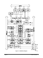
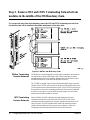
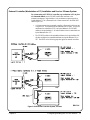
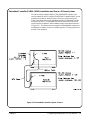
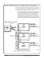
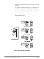
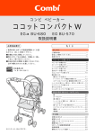
1
Agilent 75000 Series C
Agilent E1482B
VXI-MXI Bus Extender
User’s Manual
*E1482-90006*
Manual Part Number: E1482-90006
Printed in Malaysia E0806
Contents
Agilent E1482B VXI-MXI Bus Extender User’s Manual
Edition 5 Rev 2
Warranty . . . . . . . . . .
WARNINGS . . . . . . . .
Safety Symbols . . . . . .
Declaration of Conformity .
User Notes . . . . . . . . .
.
.
.
.
.
.
.
.
.
.
.
.
.
.
.
.
.
.
.
.
.
.
.
.
.
.
.
.
.
.
.
.
.
.
.
.
.
.
.
.
.
.
.
.
.
.
.
.
.
.
.
.
.
.
.
.
.
.
.
.
.
.
.
.
.
.
.
.
.
.
.
.
.
.
.
.
.
.
.
.
.
.
.
.
.
.
.
.
.
.
.
.
.
.
.
.
.
.
.
.
.
.
.
.
.
.
.
.
.
.
.
.
.
.
.
.
.
.
.
.
.
.
.
.
.
.
.
.
.
.
.
.
.
.
.
.
.
.
.
.
.
.
.
.
.
.
.
.
.
.
.
.
.
.
.
.
.
.
.
.
5
6
6
7
8
Chapter 1. Product Overview . . . . . . . . . . . . . . . . . . . . . . . . . . . . . . . . . . 13
VXI-MXI Functional Description
Features . . . . . . . . . . . . .
VMEbus Support Signals . . . .
VXI-MXI Physical Description .
Faceplate Annunciator . . . .
MXIbus Connector . . . . . .
INTX Connector . . . . . . .
SMB connectors . . . . . . .
System Reset Button . . . . .
.
.
.
.
.
.
.
.
.
.
.
.
.
.
.
.
.
.
.
.
.
.
.
.
.
.
.
.
.
.
.
.
.
.
.
.
.
.
.
.
.
.
.
.
.
.
.
.
.
.
.
.
.
.
.
.
.
.
.
.
.
.
.
.
.
.
.
.
.
.
.
.
.
.
.
.
.
.
.
.
.
.
.
.
.
.
.
.
.
.
.
.
.
.
.
.
.
.
.
.
.
.
.
.
.
.
.
.
.
.
.
.
.
.
.
.
.
.
.
.
.
.
.
.
.
.
.
.
.
.
.
.
.
.
.
.
.
.
.
.
.
.
.
.
.
.
.
.
.
.
.
.
.
.
.
.
.
.
.
.
.
.
.
.
.
.
.
.
.
.
.
.
.
.
.
.
.
.
.
.
.
.
.
.
.
.
.
.
.
.
.
.
.
.
.
.
.
.
.
.
.
.
.
.
.
.
.
.
.
.
.
.
.
.
.
.
.
.
.
.
.
.
.
.
.
.
.
.
.
.
.
.
.
.
.
.
.
.
.
.
.
.
.
.
.
.
.
.
.
.
.
.
.
.
.
.
.
.
.
.
13
16
17
17
17
17
17
18
18
Chapter 2. Configuring/Installing the VXI-MXI Module . . . . . . . . . . . . . . . . . . 19
Initial Installation Tasks . . . . . . . . . . . . . . . . . . . . . . . . . . . . . .
NOTE: Advanced Configuration . . . . . . . . . . . . . . . . . . . . . . .
Multiframe System Design . . . . . . . . . . . . . . . . . . . . . . . . . . .
Factory Default Configuration Settings . . . . . . . . . . . . . . . . . . . .
VXIbus Slot 0 . . . . . . . . . . . . . . . . . . . . . . . . . . . . . . . . .
MXIbus Terminating Resistor Networks . . . . . . . . . . . . . . . . . . .
INTX Terminating Resistor Networks . . . . . . . . . . . . . . . . . . . . .
VXIbus Logical Address . . . . . . . . . . . . . . . . . . . . . . . . . . . .
Getting Started With MXIbus Addressing . . . . . . . . . . . . . . . . . . .
Addressing VXI Modules . . . . . . . . . . . . . . . . . . . . . . . . . . .
Quick Set-Up Address Examples: 2-Frame and 3-Frame VXI-MXI Systems
Installing the VXI-MXI Module . . . . . . . . . . . . . . . . . . . . . . . .
Connecting the MXIbus Cable . . . . . . . . . . . . . . . . . . . . . . . . .
Connecting a Display Terminal to View Configuration Sequence . . . . . .
Optional Printout of Configuration Sequence . . . . . . . . . . . . . . . . .
Verification Without a Terminal or Printer . . . . . . . . . . . . . . . . . .
What If Problems are Encountered? . . . . . . . . . . . . . . . . . . . . . .
Typical Listing of Configuration Sequence . . . . . . . . . . . . . . . . . .
VMEbus Devices in VXIbus/MXIbus Systems . . . . . . . . . . . . . . . . . .
Optional Equipment . . . . . . . . . . . . . . . . . . . . . . . . . . . . . . . .
Hardware Installation Rules . . . . . . . . . . . . . . . . . . . . . . . . . . . .
Rules For Selecting Logical Addresses . . . . . . . . . . . . . . . . . . . .
Agilent E1482B User’s Manual
.
.
.
.
.
.
.
.
.
.
.
.
.
.
.
.
.
.
.
.
.
.
.
.
.
.
.
.
.
.
.
.
.
.
.
.
.
.
.
.
.
.
.
.
.
.
.
.
.
.
.
.
.
.
.
.
.
.
.
.
.
.
.
.
.
.
.
.
.
.
.
.
.
.
.
.
.
.
.
.
.
.
.
.
.
.
.
.
19
20
21
22
25
26
26
28
29
29
30
45
46
48
48
48
48
49
52
52
53
54
Table of Contents 1
Chapter 3. Switch/Jumper Configuration Reference . . . . . . . . . . . . . . . . . . . . . 57
Switch/Jumper List . . . . . . . . . . . . . . . . . . . . . . . .
VMEbus Request Level . . . . . . . . . . . . . . . . . . . .
VMEbus Timeout Level (VME BTO Level) . . . . . . . . .
VMEbus Timeout Chain Position (VME BTO Chain Position)
Interlocked Arbitration . . . . . . . . . . . . . . . . . . . . .
MXIbus System Controller . . . . . . . . . . . . . . . . . . .
MXI Controller Timeout Level . . . . . . . . . . . . . . . .
MXIbus Fairness . . . . . . . . . . . . . . . . . . . . . . . .
CLK10 Source . . . . . . . . . . . . . . . . . . . . . . . . .
CLK10 Mapping . . . . . . . . . . . . . . . . . . . . . . . .
EXT CLK SMB Input/Output . . . . . . . . . . . . . . . . .
Trigger Input Termination . . . . . . . . . . . . . . . . . . .
Front Panel Pushbutton Reset . . . . . . . . . . . . . . . . .
.
.
.
.
.
.
.
.
.
.
.
.
.
.
.
.
.
.
.
.
.
.
.
.
.
.
.
.
.
.
.
.
.
.
.
.
.
.
.
.
.
.
.
.
.
.
.
.
.
.
.
.
.
.
.
.
.
.
.
.
.
.
.
.
.
.
.
.
.
.
.
.
.
.
.
.
.
.
.
.
.
.
.
.
.
.
.
.
.
.
.
.
.
.
.
.
.
.
.
.
.
.
.
.
.
.
.
.
.
.
.
.
.
.
.
.
.
.
.
.
.
.
.
.
.
.
.
.
.
.
.
.
.
.
.
.
.
.
.
.
.
.
.
.
.
.
.
.
.
.
.
.
.
.
.
.
57
57
59
60
61
62
63
64
65
66
67
67
68
Chapter 4. Theory of Operation . . . . . . . . . . . . . . . . . . . . . . . . . . . . . . . . 69
VXIbus Address & Address Modifier Transceivers . . . .
VXIbus System Controller Functions . . . . . . . . . . . .
VXIbus Data Transceivers . . . . . . . . . . . . . . . . . .
VXIbus Control Signal Transceivers . . . . . . . . . . . .
VMEbus Requester and Arbiter Circuitry . . . . . . . . . .
TTL and ECL Trigger Lines and CLK10 Circuitry . . . . .
SYSFAIL, ACFAIL, and SYSRESET . . . . . . . . . . .
Interrupt Circuitry . . . . . . . . . . . . . . . . . . . . . .
Parity Check and Generation . . . . . . . . . . . . . . . .
A32, A24, A16, and LA Windows . . . . . . . . . . . . .
VXI-MXI Configuration Registers . . . . . . . . . . . . .
MXIbus Master Mode State Machine . . . . . . . . . . . .
MXIbus Slave Mode State Machine . . . . . . . . . . . . .
MXIbus Address/Data and Address Modifier Transceivers
MXIbus System Controller Functions . . . . . . . . . . . .
MXIbus Control Signal Transceivers . . . . . . . . . . . .
MXIbus Requester and Arbiter Circuitry . . . . . . . . . .
.
.
.
.
.
.
.
.
.
.
.
.
.
.
.
.
.
.
.
.
.
.
.
.
.
.
.
.
.
.
.
.
.
.
.
.
.
.
.
.
.
.
.
.
.
.
.
.
.
.
.
.
.
.
.
.
.
.
.
.
.
.
.
.
.
.
.
.
.
.
.
.
.
.
.
.
.
.
.
.
.
.
.
.
.
.
.
.
.
.
.
.
.
.
.
.
.
.
.
.
.
.
.
.
.
.
.
.
.
.
.
.
.
.
.
.
.
.
.
.
.
.
.
.
.
.
.
.
.
.
.
.
.
.
.
.
.
.
.
.
.
.
.
.
.
.
.
.
.
.
.
.
.
.
.
.
.
.
.
.
.
.
.
.
.
.
.
.
.
.
.
.
.
.
.
.
.
.
.
.
.
.
.
.
.
.
.
.
.
.
.
.
.
.
.
.
.
.
.
.
.
.
.
.
.
.
.
.
.
.
.
.
.
.
.
.
.
.
.
.
.
.
.
.
.
.
.
.
.
.
.
.
.
.
.
.
.
.
.
.
.
.
.
.
.
.
.
.
.
.
.
.
.
.
.
69
69
70
70
70
70
71
72
75
75
75
75
79
80
81
81
81
Appendix A. Specifications . . . . . . . . . . . . . . . . . . . . . . . . . . . . . . . . . . . 85
Electrical Characteristics .
VMEbus Modules . . . .
MXIbus Bus Transfer Rate
External Clock Input . . .
External Clock Output . .
Trigger Input . . . . . . .
Trigger Output . . . . . .
Power Requirement . . . .
Physical . . . . . . . . . .
Operating Environment .
Storage Environment . . .
Cooling Requirements . .
2 Table of Contents
.
.
.
.
.
.
.
.
.
.
.
.
.
.
.
.
.
.
.
.
.
.
.
.
.
.
.
.
.
.
.
.
.
.
.
.
.
.
.
.
.
.
.
.
.
.
.
.
.
.
.
.
.
.
.
.
.
.
.
.
.
.
.
.
.
.
.
.
.
.
.
.
.
.
.
.
.
.
.
.
.
.
.
.
.
.
.
.
.
.
.
.
.
.
.
.
.
.
.
.
.
.
.
.
.
.
.
.
.
.
.
.
.
.
.
.
.
.
.
.
.
.
.
.
.
.
.
.
.
.
.
.
.
.
.
.
.
.
.
.
.
.
.
.
.
.
.
.
.
.
.
.
.
.
.
.
.
.
.
.
.
.
.
.
.
.
.
.
.
.
.
.
.
.
.
.
.
.
.
.
.
.
.
.
.
.
.
.
.
.
.
.
.
.
.
.
.
.
.
.
.
.
.
.
.
.
.
.
.
.
.
.
.
.
.
.
.
.
.
.
.
.
.
.
.
.
.
.
.
.
.
.
.
.
.
.
.
.
.
.
.
.
.
.
.
.
.
.
.
.
.
.
.
.
.
.
.
.
.
.
.
.
.
.
.
.
.
.
.
.
.
.
.
.
.
.
.
.
.
.
.
.
.
.
.
.
.
.
.
.
.
.
.
.
.
.
.
.
.
.
.
.
.
.
.
.
.
.
.
.
.
.
.
.
.
.
.
.
.
.
.
.
.
.
.
.
.
.
.
.
.
.
.
.
.
.
.
.
.
.
.
.
.
.
.
.
.
.
.
.
.
.
.
.
.
.
.
.
.
.
.
.
.
.
.
.
.
.
.
.
.
.
85
85
85
85
86
86
86
86
86
86
86
86
Agilent E1482B User’s Manual
Appendix B. Error Messages . . . . . . . . . . . . . . . . . . . . . . . . . . . . . . . . . . 87
Reading an Instrument’s Error Queue . . . . . . . . . . . . . . . . . . . . . . . . . . . 87
Error Messages and Causes . . . . . . . . . . . . . . . . . . . . . . . . . . . . . . . . 89
Start-up Error Messages and Warnings . . . . . . . . . . . . . . . . . . . . . . . . . . 95
Appendix C. Register Definitions . . . . . . . . . . . . . . . . . . . . . . . . . . . . . . . . 101
Register Maps . . . . . . . . . . . . . . . . . . .
Register Description Format . . . . . . . . . .
Hard and Soft Reset . . . . . . . . . . . . . .
VXIbus Configuration Registers . . . . . . . . .
VXIbus ID Register . . . . . . . . . . . . . .
Device Type Register . . . . . . . . . . . . . .
VXIbus Status/Control Register . . . . . . . .
VXIbus Extender Registers . . . . . . . . . . . .
MODID Register . . . . . . . . . . . . . . . .
Logical Address Window Register . . . . . . .
A16 Window Map Register . . . . . . . . . .
A24 Window Map Register . . . . . . . . . .
A32 Window Map Register . . . . . . . . . .
Subclass Register . . . . . . . . . . . . . . . .
INTX Defined Registers . . . . . . . . . . . . . .
Interrupt Configuration Register . . . . . . . .
TTL Trigger Configuration Register . . . . .
Utility Configuration Register . . . . . . . . .
MXIbus Defined Registers . . . . . . . . . . . .
MXIbus Status/Control Register . . . . . . . .
MXIbus Lock Register . . . . . . . . . . . . .
MXIbus IRQ Configuration Register . . . . .
Drive Triggers/Read LA Register . . . . . . .
Trigger Mode Selection Register . . . . . . . .
Interrupt Status/Control Register . . . . . . . .
Status/ID Register . . . . . . . . . . . . . . .
External Trigger Port Configuration Register .
Trigger Synchronous Acknowledge Register .
Trigger Asynchronous Acknowledge Register
IRQ Acknowledge Registers . . . . . . . . . .
.
.
.
.
.
.
.
.
.
.
.
.
.
.
.
.
.
.
.
.
.
.
.
.
.
.
.
.
.
.
.
.
.
.
.
.
.
.
.
.
.
.
.
.
.
.
.
.
.
.
.
.
.
.
.
.
.
.
.
.
.
.
.
.
.
.
.
.
.
.
.
.
.
.
.
.
.
.
.
.
.
.
.
.
.
.
.
.
.
.
.
.
.
.
.
.
.
.
.
.
.
.
.
.
.
.
.
.
.
.
.
.
.
.
.
.
.
.
.
.
.
.
.
.
.
.
.
.
.
.
.
.
.
.
.
.
.
.
.
.
.
.
.
.
.
.
.
.
.
.
.
.
.
.
.
.
.
.
.
.
.
.
.
.
.
.
.
.
.
.
.
.
.
.
.
.
.
.
.
.
.
.
.
.
.
.
.
.
.
.
.
.
.
.
.
.
.
.
.
.
.
.
.
.
.
.
.
.
.
.
.
.
.
.
.
.
.
.
.
.
.
.
.
.
.
.
.
.
.
.
.
.
.
.
.
.
.
.
.
.
.
.
.
.
.
.
.
.
.
.
.
.
.
.
.
.
.
.
.
.
.
.
.
.
.
.
.
.
.
.
.
.
.
.
.
.
.
.
.
.
.
.
.
.
.
.
.
.
.
.
.
.
.
.
.
.
.
.
.
.
.
.
.
.
.
.
.
.
.
.
.
.
.
.
.
.
.
.
.
.
.
.
.
.
.
.
.
.
.
.
.
.
.
.
.
.
.
.
.
.
.
.
.
.
.
.
.
.
.
.
.
.
.
.
.
.
.
.
.
.
.
.
.
.
.
.
.
.
.
.
.
.
.
.
.
.
.
.
.
.
.
.
.
.
.
.
.
.
.
.
.
.
.
.
.
.
.
.
.
.
.
.
.
.
.
.
.
.
.
.
.
.
.
.
.
.
.
.
.
.
.
.
.
.
.
.
.
.
.
.
.
.
.
.
.
.
.
.
.
.
.
.
.
.
.
.
.
.
.
.
.
.
.
.
.
.
.
.
.
.
.
.
.
.
.
.
.
.
.
.
.
.
.
.
.
.
.
.
.
.
.
.
.
.
.
.
.
.
.
.
.
.
.
.
.
.
.
.
.
.
.
.
.
.
.
.
.
.
.
.
.
.
.
.
.
.
.
.
.
.
.
.
.
.
.
.
.
.
.
.
.
.
.
.
.
.
.
.
.
.
.
.
.
.
.
.
.
.
.
.
.
.
.
.
.
.
.
.
.
.
.
.
.
.
.
.
.
.
.
.
.
.
.
.
.
.
.
.
.
.
.
.
.
.
.
.
.
.
.
.
.
.
.
.
.
.
.
.
.
.
101
101
101
104
104
105
105
106
106
106
109
111
113
114
115
115
115
116
117
117
120
120
121
122
124
126
127
127
127
128
Appendix D. INTX/MXI Connector Pinouts . . . . . . . . . . . . . . . . . . . . . . . . . 129
Agilent E1482B User’s Manual
Table of Contents 3
Notes
4 Table of Contents
Agilent E1482B User’s Manual
Certification
Agilent Technologies certifies that this product met its published specifications at the time of shipment from the factory. Agilent
Technologies further certifies that its calibration measurements are traceable to the United States National Institute of Standards and
Technology (formerly National Bureau of Standards), to the extent allowed by that organization’s calibration facility, and to the calibration
facilities of other International Standards Organization members.
Warranty
This Agilent Technologies product is warranted against defects in materials and workmanship for a period of one (1) year from date of
shipment. Duration and conditions of warranty for this product may be superseded when the product is integrated into (becomes a part
of) other Agilent products. During the warranty period, Agilent Technologies will, at its option, either repair or replace products which
prove to be defective.
For warranty service or repair, this product must be returned to a service facility designated by Agilent Technologies. Buyer shall prepay
shipping charges to Agilent and Agilent shall pay shipping charges to return the product to Buyer. However, Buyer shall pay all shipping
charges, duties, and taxes for products returned to Agilent from another country.
Agilent warrants that its software and firmware designated by Agilent for use with a product will execute its programming instructions
when properly installed on that product. Agilent does not warrant that the operation of the product, or software, or firmware will be
uninterrupted or error free.
Limitation Of Warranty
The foregoing warranty shall not apply to defects resulting from improper or inadequate maintenance by Buyer, Buyer-supplied products
or interfacing, unauthorized modification or misuse, operation outside of the environmental specifications for the product, or improper site
preparation or maintenance.
The design and implementation of any circuit on this product is the sole responsibility of the Buyer. Agilent does not warrant the Buyer’s
circuitry or malfunctions of Agilent products that result from the Buyer’s circuitry. In addition, Agilent does not warrant any damage that
occurs as a result of the Buyer’s circuit or any defects that result from Buyer-supplied products.
NO OTHER WARRANTY IS EXPRESSED OR IMPLIED. Agilent SPECIFICALLY DISCLAIMS THE IMPLIED WARRANTIES
OF MERCHANTABILITY AND FITNESS FOR A PARTICULAR PURPOSE.
Exclusive Remedies
THE REMEDIES PROVIDED HEREIN ARE BUYER’S SOLE AND EXCLUSIVE REMEDIES. Agilent SHALL NOT BE LIABLE
FOR ANY DIRECT, INDIRECT, SPECIAL, INCIDENTAL, OR CONSEQUENTIAL DAMAGES, WHETHER BASED ON CONTRACT, TORT, OR ANY OTHER LEGAL THEORY.
Notice
The information contained in this document is subject to change without notice. Agilent Technologies MAKES NO WARRANTY OF
ANY KIND WITH REGARD TO THIS MATERIAL, INCLUDING, BUT NOT LIMITED TO, THE IMPLIED WARRANTIES OF
MERCHANTABILITY AND FITNESS FOR A PARTICULAR PURPOSE. Agilent shall not be liable for errors contained herein or for
incidental or consequential damages in connection with the furnishing, performance or use of this material. This document contains
proprietary information which is protected by copyright. All rights are reserved. No part of this document may be photocopied, reproduced,
or translated to another language without the prior written consent of Agilent Technologies, Inc. Agilent assumes no responsibility for the
use or reliability of its software on equipment that is not furnished by Agilent.
U.S. Government Restricted Rights
The Software and Documentation have been developed entirely at private expense. They are delivered and licensed as "commercial
computer software" as defined in DFARS 252.227- 7013 (Oct 1988), DFARS 252.211-7015 (May 1991) or DFARS 252.227-7014 (Jun
1995), as a "commercial item" as defined in FAR 2.101(a), or as "Restricted computer software" as defined in FAR 52.227-19 (Jun 1987)(or
any equivalent agency regulation or contract clause), whichever is applicable. You have only those rights provided for such Software and
Documentation by the applicable FAR or DFARS clause or the Agilent standard software agreement for the product involved.
Agilent E1482B VXI-MXI Bus Extender Module User’s Manual
Edition 5 Rev 2
Copyright © 1997-2006 Agilent Technologies, Inc. All Rights Reserved.
Agilent E1482B VXI-MXI Bus Extender Module User’s Manual
5
Printing History
The Printing History shown below lists all Editions and Updates of this manual and the printing date(s). The first printing of the manual
is Edition 1. The Edition number increments by 1 whenever the manual is revised. Updates, which are issued between Editions, contain
replacement pages to correct the current Edition of the manual. Updates are numbered sequentially starting with Update 1. When a new
Edition is created, it contains all the Update information for the previous Edition. Each new Edition or Update also includes a revised copy
of this printing history page. Many product updates or revisions do not require manual changes and, conversely, manual corrections may
be done without accompanying product changes. Therefore, do not expect a one-to-one correspondence between product updates and
manual updates.
Edition 1 . . . . . . . . . . . . . . . . . . . . . . . . . . . . . . . . . . . . . . . . . . . . February 1992
Edition 2 . . . . . . . . . . . . . . . . . . . . . . . . . . . . . . . . . . . . . . . . . . . . . January 1993
Edition 3 . . . . . . . . . . . . . . . . . . . . . . . . . . . . . . . . . . . . . . . . . . . . . . August 1993
Edition 4 . . . . . . . . . . . . . . . . . . . . . . . . . . . . . . . . . . . . . . . . . . . . . . August 1994
Edition 5 (Part Number E1482-90006). . . . . . . . . . . . . . . . . . . . . . . . . May 1997
Edition 5 Rev 2 (Part Number E1482-90006) . . . . . . . . . . . . . . . . . August 2006
Safety Symbols
Instruction manual symbol affixed to product.
Indicates that the user must refer to the manual for specific WARNING or CAUTION
information to avoid personal injury or damage to the product.
Alternating current (AC).
Direct current (DC).
Indicates hazardous voltages.
Indicates the field wiring terminal that must
be connected to earth ground before operating
the equipment—protects against electrical
shock in case of fault.
or
Frame or chassis ground terminal—typically
connects to the equipment’s metal frame.
WARNING
CAUTION
Calls attention to a procedure, practice, or condition that could cause bodily injury or death.
Calls attention to a procedure, practice, or condition that could possibly cause damage to
equipment or permanent loss of data.
WARNINGS
The following general safety precautions must be observed during all phases of operation, service, and repair of this product.
Failure to comply with these precautions or with specific warnings elsewhere in this manual violates safety standards of design,
manufacture, and intended use of the product. Agilent Technologies assumes no liability for the customer’s failure to comply with
these requirements.
Ground the equipment: For Safety Class 1 equipment (equipment having a protective earth terminal), an uninterruptible safety earth
ground must be provided from the mains power source to the product input wiring terminals or supplied power cable.
DO NOT operate the product in an explosive atmosphere or in the presence of flammable gases or fumes.
For continued protection against fire, replace the line fuse(s) only with fuse(s) of the same voltage and current rating and type.
DO NOT use repaired fuses or short-circuited fuse holders.
Keep away from live circuits: Operating personnel must not remove equipment covers or shields. Procedures involving the removal of
covers or shields are for use by service-trained personnel only. Under certain conditions, dangerous voltages may exist even with the
equipment switched off. To avoid dangerous electrical shock, DO NOT perform procedures involving cover or shield removal unless you
are qualified to do so.
DO NOT operate damaged equipment: Whenever it is possible that the safety protection features built into this product have been
impaired, either through physical damage, excessive moisture, or any other reason, REMOVE POWER and do not use the product until
safe operation can be verified by service-trained personnel. If necessary, return the product to an Agilent Technologies Sales and Service
Office for service and repair to ensure that safety features are maintained.
DO NOT service or adjust alone: Do not attempt internal service or adjustment unless another person, capable of rendering first aid and
resuscitation, is present.
DO NOT substitute parts or modify equipment: Because of the danger of introducing additional hazards, do not install substitute parts
or perform any unauthorized modification to the product. Return the product to an Agilent Technologies Sales and Service Office for
service and repair to ensure that safety features are maintained.
6
Agilent E1482B VXI-MXI Bus Extender Module User’s Manual
DECLARATION OF CONFORMITY
According to ISO/IEC Guide 22 and CEN/CENELEC EN 45014
Manufacturer’s Name:
Manufacturer’s Address:
Agilent Technologies, Incorporated
th
815 – 14 St. SW
Loveland, Colorado 80537
USA
Declares, that the product
Product Name:
Model Number:
Product Options:
VXIbus Extender
E1482B
This declaration covers all options of the above product(s).
Conforms with the following European Directives:
The product herewith complies with the requirements of the Low Voltage Directive 73/23/EEC and the EMC Directive 89/336/EEC
(including 93/68/EEC) and carries the CE Marking accordingly.
Conforms with the following product standards:
EMC
Standard
Limit
IEC 61326-1:1997+A1:1998 / EN 61326-1:1997+A1:1998
CISPR 11:1990 / EN 55011:1991
IEC 61000-4-2:1995+A1:1998 / EN 61000-4-2:1995
IEC 61000-4-3:1995 / EN 61000-4-3:1995
IEC 61000-4-4:1995 / EN 61000-4-4:1995
IEC 61000-4-5:1995 / EN 61000-4-5:1995
IEC 61000-4-6:1996 / EN 61000-4-6:1996
IEC 61000-4-11:1994 / EN 61000-4-11:1994
Group 1 Class A
4kV CD, 8kV AD
3 V/m, 80-1000 MHz
0.5kV signal lines, 1kV power lines
0.5 kV line-line, 1 kV line-ground
3V, 0.15-80 MHz I cycle, 100%
Dips: 30% 10ms; 60% 100ms
Interrupt > 95%@5000ms
Canada: ICES-001:1998
Australia/New Zealand: AS/NZS 2064.1
The product was tested in a typical configuration with Agilent Technologies test systems.
Safety
IEC 61010-1:1990+A1:1992+A2:1995 / EN 61010-1:1993+A2:1995
Canada: CSA C22.2 No. 1010.1:1992
UL 3111-1: 1994
1 June 2001
Date
Ray Corson
Product Regulations Program Manager
For further information, please contact your local Agilent Technologies sales office, agent or distributor.
Authorized EU-representative: Agilent Technologies Deutschland GmbH, Herrenberger Straβe 130, D 71034 Böblingen, Germany
Agilent E1482B VXI-MXI Bus Extender Module User’s Manual 7
Notes
8
Agilent E1482B VXI-MXI Bus Extender Module User’s Manual
Notes
Agilent E1482B VXI-MXI Bus Extender Module User’s Manual
9
Notes
10
Agilent E1482B VXI-MXI Bus Extender Module User’s Manual
About This Manual
Manual Content
Chapter 1:
Product Overview
This manual contains information on the applications of the Agilent E1482B
VXI-MXI Bus Extender Module. It is part of a manual set that includes the C-Size
VXIbus Systems “ Installation and Getting Started Guide” and various plug-in
module user’s manuals.
This chapter contains a functional, electrical, and physical description of the
Agilent E1482B VXI-MXI Bus Extender Module
Chapter 2:
Configuring/Installing the
VXI-MXI Module
This chapter provides configuring and installation information for installing your
VXI-MXI modules in C-size mainframes. It provides the system set-up procedure
for a default system configuration including the address windows.
Chapter 3:
Switch/Jumper
Configuration Reference
This chapter provides reference information you can use to change the default
configuration settings of the VXI-MXI module. Switches and jumpers discussed in
this chapter do not need to be changed to set up a working system. They can be
changed to meet special requirements of your test system.
Chapter 4:
Theory of Operation
Appendix A:
Specifications
Appendix B:
Error Messages
This chapter discusses the major elements of the VXI-MXI in detail.
This appendix contains a list of the VXI-MXI Bus Extender Module’s operating
specifications.
This appendix lists the error messages associated with the Command Module and
their possible causes.
Appendix C:
Register Definitions
This appendix contains a detailed description of the operational characteristics and
programming requirements for the VXI-MXI Bus Extender Module’s registers.
Appendix D:
INTX/MXI Connector
Pinouts
This appendix contains the pinouts for the INTX and MXI connectors for reference
purposes only.
Agilent E1482B User’s Manual
About This Manual 11
Notes
12 About This Manual
Agilent E1482B User’s Manual
Chapter 1
Product Overview
About this Chapter
This chapter describes the VXI-MXI features, lists the contents of your VXI-MXI
kit, and explains how to unpack the VXI-MXI kit.
•
•
•
•
VXI-MXI Functional Description . . . . . . . . . . . . . . . . . . . . .
Features . . . . . . . . . . . . . . . . . . . . . . . . . . . . . . . . . . . . . . . . . .
VMEbus Support Signals . . . . . . . . . . . . . . . . . . . . . . . . . . . .
VXI-MXI Physical Description . . . . . . . . . . . . . . . . . . . . . . .
13
16
17
17
1
VXI-MXI Functional
Description
The VXI-MXI is a C-size extended class VXIbus extender device that interfaces the
VXIbus to the MXIbus. The VXI-MXI interface module uses address mapping to
transparently translate bus cycles on the VXIbus system bus (VMEbus) to the
MXIbus and vice versa.
In simplest terms, the VXI-MXI can be thought of as a bus translator that converts
VXIbus signals into appropriate MXIbus signals. Expressed in MXIbus
terminology, the VXI-MXI implements a MXIbus interface to communicate with
other MXIbus devices. Expressed in VMEbus terminology, the VXI-MXI is an
interface to the outside world.
A functional block diagram of the VXI-MXI is shown in Figure 1-1. The major
components of the VXI-MXI are discussed in greater detail in Chapter 4, “ Theory
of Operation.”
The VXI-MXI is an extended class register-based VXIbus device with optional Slot
0 capability so that it can reside in any slot in a C-size or D-size VXIbus chassis.
The VXI-MXI converts A32, A24, A16, D32, D16, and D08(EO) VXIbus cycles
into MXIbus cycles and vice versa. The VXI-MXI has four address windows that
map into and out of the VXIbus mainframe. These four windows represent the three
VMEbus address spaces (A32, A24, and A16) plus a dedicated window for
mapping the VXIbus configuration space (the upper 16 kilobytes of A16 space).
The MXIbus is a multidrop system bus that connects multiple devices at the
hardware bus level in a software-transparent manner. Multiple VXIbus mainframes
with VXI-MXI interfaces can be connected to form a single multiframe VXIbus
system.
Multiple MXIbus devices are tightly coupled by mapping together portions of each
device’s address space and interlocking the internal hardware bus cycles across the
MXIbus. The window address circuitry on each MXIbus device monitors internal
local bus cycles to detect bus cycles that map across the MXIbus. Similarly,
external MXIbus cycles are monitored to detect MXIbus cycles that map into the
VXIbus system. MXIbus devices can operate in parallel at full speed over their
local system bus and need to synchronize operation with another device only when
addressing or being addressed by a resource located on another MXIbus device. The
Chapter 1
Product Overview
13
MXIbus device originating the transaction must gain ownership of the MXIbus and
of the local bus in the target MXIbus device. All hardware bus cycles are then
interlocked across the MXIbus and local buses to complete the transfer.
The VXI-MXI INTX daughter card contains three registers which reside in the
VXI-MXI Configuration Space. The INTX Interrupt Configuration Register, the
INTX Trigger Configuration Register, and the INTX Reset Configuration Register
configure the mapping of the VMEbus interrupt lines, the VXIbus trigger lines, and
the SYSRESET, SYSFAIL, and ACFAIL lines to and from the INTX connector.
The interrupt logic maps the VMEbus interrupt lines to and from the corresponding
INTX interrupt lines. In conjunction with the VXI-MXI circuitry, the interrupt
requests routed between VXIbus mainframes through the INTX connector can be
transparently serviced by interrupt handlers in VXIbus mainframes other than the
mainframe from which the request was generated. This process takes advantage of
transparent MXIbus interrupt acknowledge cycles.
When an interrupt request received from across the INTX is driven on the
corresponding VMEbus interrupt line, and an interrupt handler in the receiving
VXIbus mainframe generates an interrupt acknowledge cycle for that interrupt
request, the interrupt acknowledge cycle is transparently converted to a MXIbus
interrupt acknowledge cycle for that interrupt request level. Similarly, when a
VMEbus interrupt line is driven out of the VXIbus mainframe across the INTX
connection, an interrupt handler in another VXIbus mainframe can generate an
interrupt acknowledge cycle to handle that interrupt. The VXI-MXI in the
requesting mainframe will recognize that the MXIbus interrupt acknowledge cycle
is for the request it is driving, and will convert the cycle into a VMEbus interrupt
acknowledge cycle which can service the VMEbus interrupt request.
The trigger control logic maps the VXIbus trigger lines to and from the
corresponding INTX trigger lines. When mapping high speed trigger signals across
the INTX connection, total cable length in the connection should be limited to 12
meters.
The system reset control circuitry maps the VMEbus signals SYSRESET,
SYSFAIL, and ACFAIL to the corresponding signals on the INTX connection.
The CLK10 Control circuitry routs the VMEbus 10MHz signal to and from the
INTX connection. The configuration of the CLK10 mapping is controlled by three
switches on the INTX daughter card. In order to maintain the 10MHz signal, the
INTX CLK10 signal must be limited to a total of 12 meters of cable.
The INTX connector is a shielded 44-pin connector. Cables can be connected
point-to-point or daisy-chained between devices.
14
Product Overview
Chapter 1
Figure 1-1. VXI-MXI Block Diagram.
Chapter 1
Product Overview
15
The interrupt and reset signals are extended with standard MXIbus tranceivers.
These tranceivers are open collector devices that generate precise trapezoidal
waveforms with typical risetimes of nine nanoseconds. The trapezoidal shape
reduces crosstalk between adjacent signals. The receivers have built-in low pass
filters to remove noise, and a high speed comparator that recognizes the trapezoidal
shaped signal from noise. MXIbus specifies a maximum of 8 devices on one link
with total cable lengths up to 20 meters and data rates up to 20Mbytes/sec.
The high speed signals are extended by the INTX daughter card with RS-485
tranceivers. RS-485 is differential and permits data rates up to 10Mbaud at distances
up to 12 meters. It is also multi-point, meaning that there can be multiple (up to 32)
drivers and receivers on a signal line.
1
Features
The VXI-MXI has the following features:
• Interfaces the VXIbus to the MXIbus (32-bit Multisystem Extension
Interface bus)
• Extends VXIbus to multiple mainframes, external MXIbus-equipped
instruments, and external MXIbus-equipped personal computers (PCs)
• Multiple VXIbus mainframes appear as a single VXIbus system
• Integrated block mode for high-performance data transfers
• Supports dynamic configuration of VXIbus devices
• Interlocked bus operation for prevention of deadlock conditions
• Daughter-card connector scheme gives additional functionality
• Fully compatible with VXIbus and MXIbus specifications
• No restrictions on Commander/Servant hierarchy or physical location of
devices.
• Extends the seven VMEbus IRQ interrupts with MXIbus (trapezoidal)
tranceivers.
• Extends the VMEbus signals SYSRESET, SYSFAIL, and ACFAIL with
MXIbus tranceivers.
• Extends the eight VXIbus trigger lines with RS-485 tranceivers.
• Extends the VXIbus CLK10 signal with RS-485 tranceivers.
• Supports transparent interrupt acknowledge cycles for interrupt lines driven
and received across the INTX connection.
16
Product Overview
Chapter 1
1
VMEbus Support
Signals
The VXI-MXI generates all the support signals required by the VMEbus:
• VMEbus controller functions:
– 16-MHz system clock driver
– VME bus timeout (BTO)
– Data transfer bus arbiter (PRI ARBITER)
– Interrupt acknowledge daisy-chain driver
– Pushbutton system reset switch
• VMEbus master capabilities:
– Access to A16, A24, and A32 address space
– D8(EO), D16, and D32 accesses
– Release-on-Request bus requester (jumper-selectable arbitration level)
• VMEbus slave accesses:
– A16, A24, and A32 address space
– D8(EO), D16, and D32 accesses
• VXIbus Slot 0 functions:
– 10-MHz clock
– MODID register
– TTL and ECL Trigger line support
1
VXI-MXI Physical
Description
Faceplate Annunciator
The VXI-MXI occupies one C-Size mainframe slot. The module’s faceplate has
annunciators, clock and trigger connectors and interface ports which are described
below and illustrated in Figure 1-2.
There are three annunciators on the VXI-MXI faceplate which indicate the
following:
• FAILED LED indicates that the VMEbus SYSFAIL line is asserted.
• VME ACCESS LED indicates when the VXI-MXI is accessed from the
VXIbus.
• MXI ACCESS LED indicates when the VXI-MXI is accessed from the
MXIbus.
MXIbus Connector
INTX Connector
Chapter 1
This connector lets you connect the MXI-VXI to another MXI-VXI in your system.
This connector lets you connect the expanded interrupt functions of the MXI-VXI
to another MXI-VXI in your system.
Product Overview
17
SMB connectors
The three SMB Connectors provide trigger input and output, and external clock
input and output as required. The external clock SMB connector is configurable for
either input or output.
• External clock input or output (configurable)
• Trigger output
• Trigger input
System Reset Button
The System Reset button lets you return the MXI-VXI to its power-on state.
Figure 1-2. VXI-MXI Faceplate Layout.
18
Product Overview
Chapter 1
Chapter 2
Configuring/Installing the VXI-MXI Module
About this Chapter
This chapter describes the configuration and installation of VXI-MXI modules. The
module is shipped from the factory configured for installation in slot 0 of an
extender mainframe. You must reconfigure the VXI-MXI module used in the root
mainframe.
1
Initial Installation
Tasks
Before installing the VXI-MXI in the VXIbus mainframe, the following items must
be configured properly:
• VXIbus Slot 0 (switches S1 and S8 must be set correctly for each module or
damage can result - see Steps 1 and 2 of the installation procedure).
• MXIbus and INTX Terminating Networks (you must remove these if the
module is in the middle of the MXIbus daisy chain - see Step 3).
• VXIbus Logical Address (factory setting on each module is logical address
1; you must set all VXI-MXI module addresses and other VXI module
addresses in the system correctly - see Step 4).
Figure 2-1. Initial Installation Tasks.
Chapter 2
Configuring/Installing the VXI-MXI Module
19
NOTE:
Advanced
Configuration
There are many configuration switches and jumpers that we do not recommend you
change until you have verified system operation using the factory default settings.
The purpose for this is to establish the address windows properly for all mainframes
and to verify that the resource manager can configure the system before too many
configuration changes are made. You can troubleshoot from the verified default
configuration should you encounter operational problems after reconfiguring any of
the following items.
Refer to Chapter 3 for additional configuration information. In most cases, these
items do not need to be changed from their factory default settings.
•
•
•
•
•
•
•
•
•
•
•
•
VMEbus Request Level (jumpers W1, W2, W3, W4, and W5)
VMEbus Timeout Level (jumper W8)
VMEbus Timeout Chain Position (jumper W7)
Interlocked Arbitration (slide switch S3)
MXIbus System Controller (slide switch S4)
MXIbus System Controller Timeout Level (jumper W6)
MXIbus Fairness (slide switch S2)
CLK10 Source (jumpers W9 and W10 - accessible through the connector
edge of the VXI-MXI module)
CLK10 Mapping (slide switches W1, W2, and W3 on the daughter board)
EXT CLK SMB Input/Output (slide switch S6)
Trigger Input Termination (slide switch S5)
Front Panel Pushbutton System Reset (slide switch S7)
Figure 2-2. VXI-MXI Parts Locator Diagram.
20
Configuring/Installing the VXI-MXI Module
Chapter 2
CAUTION
The VXI-MXI is shipped from the factory configured to be installed into
Slot 0 of your VXIbus mainframe. Installing your VXI-MXI into any slot
other than Slot 0 without reconfiguring the VXI-MXI for non-slot 0
(switches S1 and S8) can damage the VXI-MXI, the VXIbus backplane,
or both. See Figure 2-6 for S1 and S8 non-slot 0 switch settings.
Multiframe System
Design
Before you begin configuring the VXI-MXI modules, you must determine what
your multiframe system will look like. With this informtion you know which
VXI-MXI modules are slot 0 modules and which module is non-slot 0 and you can
begin configuration. Figure 2-3 illustrates a VXI-MXI system using a command
module as resource manager.
NOTE
Agilent Technologies does not recommend using more than one level of extensions
below the root level because of the complexity of multi-level VXI-MXI installation
and the decrease in system performance in a multi-level system.
Figure 2-3. VXI-MXI System with VXIbus Multiframe RM.
Chapter 2
Configuring/Installing the VXI-MXI Module
21
Factory Default
Configuration Settings
Table 2-1 shows switch settings on the VXI-MXI Module for operation when the
resource manager is in another mainframe (Extender Mainframe column - these are
default settings shipped from the factory - see Figure 2-4). The table also shows
(shaded) what switches/jumpers to change to configure the module for a mainframe
where there is an embedded controller or a slot 0 Command Module provided as
resource manager (Root Mainframe columns - see Figure 2-5). Also shaded in the
extender mainframe column is a note reminding you to remove all MXIbus and
INTX terminating resistor networks for mid-frame modules in a system that is three
mainframes or larger.
Table 2-1. VXI-MXI Module Configuration Settings.
Root Mainframe
Root Mainframe
Resource Manager:
a) E1405B/1406A Cmd Module
in slot 0
(see Figures 2-9 and 2-16)
b) V/382 Embedded Controller
in slots 0 and 1
(see Figure 2-13)
Resource Manager:
Agilent RADI-EPC7
Embedded Controller
in slots 1 and 2
(see Figure 2-15)
Extender Mainframe
(Factory Default Settings)
NOTE:
VXI-MXI Module
is Configured for an
Extender Mainframe
from the factory.
Switch or Jumper
Switches S1, S8
(VXIbus Slot 0)
Figure
2-6a
All Networks Installed
(in first and last VXI-MXI
modules in the daisy chain)
MXIbus Terminating Networks
and
2-1 &
2-7
INTX Terminating Networks
Jumpers W1, W2, W3, W4, W5
(VMEbus Request Level)
Jumper W6
(VME BTO Level)
Jumper W7
(VME BTO Chain Position)
Switch S3
(Interlocked Arbitration)
Switch S4
(MXIbus System Controller)
Jumper W8
(MXI Controller Timeout Level)
Switch S2
(MXIbus Fairness)
Jumpers W9, W10
(CLK10 Source)
Switches W1, W2, W3
(CLK10 Mapping)
Switch S6
(Ext Clk SMB)
Switch S5
(Trigger Input Termination)
Switch S7
(Front Panel Pushbutton)
22
(VXI-MXI in slot 0)
Description
Slot 0
3-1a
NOTE:
Remove all MXI and INTX
networks from mid-frame
modules (see Step 3).
Level 3 requester
(Non-Slot 0 VXI-MXI)
Figure
Description
2-6b
Non-slot 0
(VXI-MXI in slot 0)
Figure
Description
2-6a
Slot 0
2-1 &
2-7
MXIbus Networks
Installed
2-1 &
2-7
MXIbus Networks
Installed
2-1 &
2-7
INTX Networks
Installed
2-1 &
2-7
INTX Networks
Installed
3-2a
VME timeout =100µsec
3-2b
VME timeout 200µsec
3-2b
VME timeout =200µsec
3-3a
1 extender, slot 0
3-3b
1 extender, non-slot 0
3-3a
1 extender, slot 0
3-6b
Interlocked
3-7a
Not MXI bus controller
3-7b
MXI bus controller
3-7b
MXI bus controller
3-8d
MXI bus timeout disabled
3-8a
MXI bus timeout
100µsec
3-8a
MXI bus timeout
100µsec
3-10c
Do not source CLK10
3-10a
On-board 10MHz
VXI-MXI installed in
slot 0
3-9a
3-10a
Fairness enabled
On-board 10MHz VXI-MXI
installed in slot 0
3-11a
CLK10 mapping disabled
3-12a
Output external clock
3-13a
Trigger 50Ω terminated
3-14a
SYSRESET* asserted
Configuring/Installing the VXI-MXI Module
Chapter 2
STEP 1. Set up all Extender Mainframe VXI-MXI Modules.
For extender (remote) mainframe VXI-MXI modules (slot 0 modules), leave the default switch and
jumper settings as shipped by the factory (except for setting the logical address which is described
later). After verifying MXIbus operation you can change settings from the default to match your system
requirements (more on this later).
Figure 2-4. Extender VXI-MXI Settings (DEFAULT).
Chapter 2
Configuring/Installing the VXI-MXI Module
23
Step 2. Set up the Root Mainframe VXI-MXI Module.
The " Root" mainframe has the resource manager in slot 0 (exceptions are if you are using the EPC-7
embedded controller or an external controller with an EISA-MXI card - see Step 4 Quick Set-Up
figures). Change only the shaded switches/jumpers to configure the VXI-MXI Module to be used in the
root mainframe (non-slot 0). You must change switches S1 and S8 to configure for non-slot 0 use or
damage can occur. The following section provides more information on slot 0 and non-slot 0 modules.
NOTE: If you are using an external controller (e.g. Series 700 workstation or PC with an EISA-MXI
card), all VXI-MXI modules are set up for extender mainframes (see Step 4 External Controller Quick
Set-Up figures for 2-frame and 3-frame systems). Set up all VXI-MXI modules as described in Step 1.
Figure 2-5. Root (Local) VXI-MXI Settings.
24
Configuring/Installing the VXI-MXI Module
Chapter 2
CAUTION
VXIbus Slot 0
Do not install a module configured for Slot 0 into another slot without
reconfiguring it for Non-Slot 0 use (e.g. Local mainframe). Doing so
can result in damage to the module, the VXIbus backplane, or both.
The VXI-MXI is shipped from the factory configured to be installed in Slot 0 of a
VXIbus extender mainframe. If another module is already in Slot 0, you must
decide which module will be the Slot 0 device and reconfigure the other module for
Non-Slot 0 use.
It is recommended you use the interlocked arbitration bus mode for both slot 0 and
non-slot 0 VXI-MXI modules. Refer to the Interlocked Arbitration Mode section
in Chapter 3 for a description of the optional normal bus mode. Figure -6(a) shows
the default configuration settings for the VXI-MXI installed as the Slot 0 device. To
configure the VXI-MXI as a Non-Slot 0 device, change slide switches S1 and S8 as
depicted in Figure 2-6(b).
Figure 2-6. VXIbus Slot 0 Selection
When the VXI-MXI is installed in Slot 0, it becomes the VMEbus System
Controller, meaning that it has VMEbus Data Transfer Bus Arbiter capability (PRI
ARBITER) and that it drives the 16-MHz VMEbus system clock. The VMEbus
Data Transfer Bus Arbiter circuitry accepts bus requests on all four VMEbus
request levels, prioritizes the requests, and grants the bus to the highest priority
requester. The VMEbus system clock is driven by an onboard 16-MHz oscillator
with a 50%±5% duty cycle.
The VXIbus specification defines several additional functions for devices installed
in the Slot 0 position. A Slot 0 device must implement a 16-bit MODID register to
control and monitor the VXIbus MODID lines. Slot 0 cards must also have 16.9 k
pull-up resistors on each VXIbus MODID line. If the card is not in Slot 0, the
MODID0 line on that card must be pulled down to ground with a 825 Ω resistor.
The VXIbus Resource Manager (RM) can identify whether the VXI-MXI is located
in Slot 0 by reading the VXIbus Model Code in the Device Type Register. If the
VXIbus Model Code for the VXI-MXI is hex 0FE, the module is in Slot 0; if the
code is hex 8FE, the module is not in Slot 0.
Chapter 2
Configuring/Installing the VXI-MXI Module
25
Step 3. Remove MXI and INTX Terminating Networks from
modules in the middle of the MXIbus daisy chain.
For systems with more than two mainframes, remove the MXI and INTX terminating networks from
the module(s) that will be installed in the middle mainframe(s) of the daisy chain.
Figure 2-7. MXIbus and INTX Daisy Chain
MXIbus Terminating
Resistor Networks
The MXIbus is a matched impedance bus and requires termination networks at the
first and last device in the MXIbus daisy-chain. These internal plug-in resistor
packages minimize reflections caused by impedance discontinuities at the ends of
the cables and therefore, are located at the MXIbus connectors.
The VXI-MXI is shipped from the factory with terminating SIP resistor networks
installed. If the VXI-MXI will be the first or last device in the MXIbus daisy-chain,
you should leave these internal terminators in place. If the VXI-MXI is not going to
be an end device, remove the terminating resistor networks from their sockets and
store them in a safe place in case the MXIbus system changes. All six MXIbus
networks must be either installed or removed.
INTX Terminating
Resistor Networks
26
Like the MXIbus, the INTX cables have matched impedance and require
termination networks at the first and last devices in the INTX chain. These
terminations minimize the reflections caused by impedance discontinuities at the
ends of the cable. The INTX daughter board comes with terminating resistors
installed. If the daughter board is not going to be an end device, remove the
terminating resistor networks and store them with the MXI networks.
Configuring/Installing the VXI-MXI Module
Chapter 2
Installing MXI and INTX Terminating Networks.
MXIbus and INTX Terminating Networks are shipped installed. They are removed if required by
Step 3. Use this information to install the networks correctly and assure proper module operation.
NOTE
MXI and INTX Terminating Networks must be installed in their correct locations
for thre modfule to operate properly. Pin #1 orientation is not critical (see
(ORIENTATION NOTE) but location is.
NOTE:
Some 10-pin INTX networks
with pin #1 common may be
identified by a black stripe
on the body.
Verify that you have the
correct networks in the
correct location by
checking the resistor
continuity before installing.
Chapter 2
Configuring/Installing the VXI-MXI Module
27
Step 4. Set the addresses for the VXI-MXI Modules, the
Resource Manager and other modules of your system.
You must set addresses that allow the resource manager to configure the system according the VXI
rules. This step contains QUICK START sections that show you how to address 2-frame and 3-frame
systems. These sections are divided into examples that show setups for systems using a command
module, an embedded controller (both an Agilent E1499 V/382 and an Agilent RADI-EPC7) and
external controllers with MXIbus modules.
VXIbus Logical
Address
Each device in a VXIbus/MXIbus system is assigned a unique number between 0
and 255. This 8-bit number, called the logical address, defines the base address for
the configuration registers located on the device. With unique logical addresses,
each VXIbus device in the system is assigned 64 bytes of configuration space in the
upper 16 kilobytes of A16 space.
Some VXIbus devices have dynamically configurable logical addresses. These
devices have an initial logical address of 255, which indicates that they can be
dynamically configured. While the VXI-MXI does support dynamic configuration
of VXIbus devices within its mainframe, it cannot itself be dynamically configured.
Therefore, do not set the logical address for the VXI-MXI to 255.
The VXIbus RM has Logical Address 0 by definition. The VXI-MXI does not
have VXIbus RM capability, so do not set the logical address for the VXI-MXI to 0.
See the following section "Getting Started With MXIbus Addressing" for
configuring addresses for a multiple mainframe VXIbus/MXIbus system.
An 8-bit DIP switch at position U46 selects the logical address for the VXI-MXI.
Refer to Figure 2-2 to find the location of this DIP switch. The metal enclosure
surrounding the VXI-MXI has a cut-out for this switch, so you do not need to
remove the metal enclosure to change this switch setting. The ON position on the
DIP switch corresponds to a logic value of 0, and the OFF position corresponds to a
logic value of 1. This switch is set at the factory to a default logical address of 128.
Verify that the logical address assigned to the VXI-MXI is not used by any other
statically configured VXIbus device in your system. Remember that logical
addresses 0 and 255 are not allowed for the VXI-MXI. Figure 2-8 shows switch
settings for logical address decimal 1 and 192 (hex 1 and hex C0).
28
Configuring/Installing the VXI-MXI Module
Chapter 2
Figure 2-8. Logical Address Selection.
Getting Started With
MXIbus Addressing
NOTE
You must structure your system and set the addresses such that the system resource
manager (RM) can configure the address window according to VXI rules. If you
set addresses that violate VXI rules, the RM cannot configure the system. It is the
user’s responsiblilty to set addresses that comply with VXI rules. Addressing rules
are discussed in this chapter following the Quick Set-Up sections.
Before you begin setting the logical addresses of the devices in your
VXIbus/MXIbus system, you must determine the tree configuration of your system.
The basic configuration for a MXIbus multiframe system is shown in Figure 2-3.
The location of the multiframe RM constitutes the root of the system tree. MXIbus
links connected to the root mainframe form level 1 of the tree.
A second VXI-MXI module in a level 1 mainframe with a MXIbus link connected
to another mainframe forms level 2. Agilent Technologies does not recommend
using more than one level of extensions below the root level because of the
complexity of multi-level VXI-MXI installation and the decrease in system
performance in a multi-level system.
Addressing VXI
Modules
C-SCPI Users (with register-based drivers): You can set VXI modules to any
address when using an embedded controller (e.g. Agilent V/382 or Agilent
RADI-EPC7) or an external controller with a MXI interface (e.g. HP series 700
workstation with E1489I MXIbus). They are able to recognize a module as an
instrument regardless of its address.
GPIB Users: A system using an GPIB controller and an Agilent E1405/E1406
Command Module as the resource manager requires instrument identifier addresses
(address divisible by 8). The command module identifies instruments when it
encounters an address divisible by 8. You should set an instrument to addresses
that are boundaries of 8 when the Agilent E1405 or E1406 is used as the resource
manager.
Chapter 2
Configuring/Installing the VXI-MXI Module
29
Quick Set-Up Address
Examples: 2-Frame
and 3-Frame VXI-MXI
Systems
Quick Set-Up
For 2-Frame Systems
There are a number of rules that govern the definition of address windows. If you
are using two or three mainframes, this section provides information that will help
you set up the address windows for most 2-frame or 3-frame VXI-MXIbus systems
without having to learn all the rules and how they apply. You may want to review
the reference information describing these rules at the back of this chapter to
understand why the addresses are set as they are.
This section provides information on setting up a basic 2-frame VXI-MXI system.
Table 2-2 and Figure 2-24 illustrate the boudaries allowed for address windows.
Allocate the address range 0 - 127 to the root mainframe (i.e. set addresses for
modules in the root mainframe to addresses in this range). Allocate the address
range 128 - 255 to the extended mainframe.
Command Module (E1405B or E1406A) Installation and Use in a 2-Frame System.
NOTE
A system using a command module as the resource manager identifies instruments
by an instrument identifier address. Instrument identifier addresses are those
divisible by 8 and must be used if you are using an Agilent E1405 or E1406
Command Module as the resource manager.
• ROOT MAINFRAME: Set the VXI-MXI module to address 2. Set other
VXI modules in the root mainframe to addresses below 128. Note: The
resource manager must be at address 0.
• EXTENDED MAINFRAME: Set the VXI-MXI module address to
address 128.
GPIB Cable
Figure 2-9. Command Module System, 2-Frame.
30
Configuring/Installing the VXI-MXI Module
Chapter 2
External Controller (Workstation or PC) Installation and Use in a 2-Frame System.
For systems using an EXTERNAL controller (e.g. workstation or PC) in place
of a command module, set the VXI-MXI module that interfaces to the
workstation/computer to logical address 1 (the workstation/computer must be at
logical address 0). This is illustrated in the 1-frame connection to the EISA-MXI
card in Figure 2-10.
• A 2-frame system using an external controller is illustrated in the lower part
of Figure 2-10. This system splits the addresses into two parts. For the root
mainframe, the workstation or PC is at logical address 0, the VXI-MXI
module is at logical address 1. All other modules in the root mainframe use
logical addresses 64 to 127.
• The VXI-MXI module in the extended mainframe is at logical address 128;
all other modules in the extended mainframe use logical addresses 129 to
255. The NOTE on the following page also applies to external controllers.
Figure 2-10. External Controller System, 2-Frame.
Chapter 2
Configuring/Installing the VXI-MXI Module
31
The following shows a 1-frame MXIbus system connected to a Series 700 workstation. This diagram depicts the system
shown in the top of figure 2-10.
Figure 2-11. Series 700 Workstation/MXI Installation.
32
Configuring/Installing the VXI-MXI Module
Chapter 2
Embedded Controller E1499A (V/382) Installation and Use in a 2-Frame System.
For systems using an Agilent E1499A (V/382) EMBEDDED controller as the
resource manager in place of an Agilent E1405/E1406 Command Module, the root
mainframe is the same as shown in Figure 2-9 except you replace the Agilent
E1406 Command Module with the embedded controller (the embedded controller
may require two slots). The embedded controller becomes the slot 0 device and
system controller (at address 0) and the address windows can be divided as shown
in Figure 2-12. This illustration shows an Agilent E1499 embedded computer and
the addresses the modules are set to for MXIbus operation. The next page shows a
pictorial of this installation.
Figure 2-12. Embedded Controller System, 2-Frame.
Chapter 2
Configuring/Installing the VXI-MXI Module
33
Figure 2-13. Installation of the V/382.
34
Configuring/Installing the VXI-MXI Module
Chapter 2
Embedded Controller (RADI-EPC7) Installation and Use in a 2-Frame System.
For systems using an Agilent RADI-EPC7 EMBEDDED controller as the resource
manager in place of an Agilent E1405/E1406 Command Module, the root
mainframe differs from Figure 2-9. You replace the Agilent E1406 Command
Module with the embedded controller (the embedded controller requires two slots)
but you must install the VXI-MXI module in slot 0 which becomes the slot 0
device at address 1. The system controller (at address 0) is the EPC7. The address
windows can be divided as shown in Figure 2-14. This illustration shows an
Agilent RADI-EPC7 embedded computer and the addresses the modules are set to
for MXIbus operation. The next page shows a pictorial of this installation.
NOTE
The EPC7 Start Up Resource Manager does not allow statically configured devices
to be located at address 255. Therefore, a MXI window with the EPC7 cannot
include address 255 and should use 191 as its largest address (see below).
Figure 2-14. Embedded (EPC7) System, 2-Frame.
Chapter 2
Configuring/Installing the VXI-MXI Module
35
Figure 2-15. EPC7 and VXI-MXI Module Installation.
36
Configuring/Installing the VXI-MXI Module
Chapter 2
Quick Set-Up
For 3-Frame Systems
This section provides information on setting up a basic 3-frame VXI-MXI system.
The most straight forward approach for three frames is to divide the address space
into three sections. It is not possible to divide the address space into three equal
segments because of the critical boundary at address 128 (see Table 2-2 and
Figures 2-16 and 2-24).
Command Module (E1405B or E1406A) Installation and Use in a 3-Frame System.
• ROOT MAINFRAME: Set the VXI-MXI module to address 2. It does not
have to be an instrument identifier address (e.g. divisible by 8; instrument
identifiers are important only if you are using an E1405 or E1406 Command
Module as the resource manager). Set other VXI modules in the root
mainframe to addresses below 128. Note: the resource manager must be at
address 0.
• FIRST EXTENDED MAINFRAME: Set the VXI-MXI module address to
address 128. You can reserve address 128 as an instrument identifier for
another VXI module in the first extended mainframe (see note below). Set
all other VXI modules to addresses between 128 and 191 (do not duplicate
the VXI-MXI address). The upper half of the address space is divided into
two address windows of 64 addresses each (one for the first extended
mainframe and one for the second extended mainframe).
NOTE
Note that a window size of 64 provides you with only eight (8) instrument
identifiers for use with the E1405/E1406.
• For the first extended mainframe whose window is 128 - 191, this includes
address 128 as one of the eight.
• For the second extended mainframe whose window is 192 - 255, this
includes address 192 as one of the eight.
The address does not have to be the first address of the window but in general, it is
easier to set the VXI-MXI module address to the first address of the window. If you
want to reserve address 128 or 192 as an instrument identifier in either window, set
the VXI-MXI module to address 129 and 193 respectively.
• SECOND EXTENDED MAINFRAME: Set the VXI-MXI module
address to 192. You can reserve address 192 as an instrument identifier for
another VXI module in the second extended mainframe (see the above note).
Set all other VXI modules to addresses between 192 and 255 (do not
duplicate the VXI-MXI address). Note that a window size of 64 provides
you with only eight (8) instrument identifiers for use when an
Agilent E1405/E1406 is used as the resource manager.
Chapter 2
Configuring/Installing the VXI-MXI Module
37
Command Module (E1405B or E1406A) Installation and Use in a 3-Frame System.
GPIB Cable
Figure 2-16. Command Module System, 3-Frame.
38
Configuring/Installing the VXI-MXI Module
Chapter 2
External Controller (Workstation or PC) Installation and Use in a 3-Frame System.
For systems using an EXTERNAL controller (e.g. workstation or PC), always set
the VXI-MXI module that interfaces to the workstation/computer to logical address
2 (the workstation/computer must be at logical address 0). This is illustrated in the
connection to the EISA-MXI card Figure 2-17. Also see Figure 2-11.
• This system splits the addresses into three address windows of 64 addresses
each. For the root mainframe, the workstation or PC is at logical address 0,
the VXI-MXI module is at logical address 2. All other modules in the root
mainframe use logical addresses 64 to 127. The VXI-MXI module in the
first extended mainframe is at logical address 128; all other modules in the
first extended mainframe use logical addresses 129 to 191. The VXI-MXI
module in the second extended mainframe is at logical address 192; all other
modules in the second extended mainframe use logical addresses 193 to 255.
Figure 2-17. External Controller System, 3-Frame.
Chapter 2
Configuring/Installing the VXI-MXI Module
39
Embedded Controller (E1499A V/382) Installation and Use in a 3-Frame System.
For systems using a V/382 EMBEDDED controller in place of an
Agilent E1405/E1406 Command Module, the root mainframe shown in Figure
2-18 replaces the Agilent E1406 Command Module with the embedded controller
(the embedded controller may require two slots). The embedded controller
becomes the slot 0 device and system controller (at address 0) and the address
windows can be divided as shown in Figure 2-18. This illustration shows an
Agilent E1499 embedded computer and the addresses the modules are set to for
MXIbus operation. Also see Figure 2-13.
Figure 2-18. Embedded Controller System, 3-Frame.
40
Configuring/Installing the VXI-MXI Module
Chapter 2
Embedded Controller (RADI-EPC7) Installation and Use in a 3-Frame System.
For systems using a RADI-EPC7 EMBEDDED controller in place of an
Agilent E1405/E1406 Command Module, the root mainframe shown in Figure
2-19 replaces the Agilent E1406 Command Module with the embedded controller
(the embedded controller may require two slots). The embedded controller
becomes the slot 0 device and system controller (at address 0) and the address
windows can be divided as shown in Figure 2-19. This illustration shows an EPC7
embedded computer and the addresses the modules are set to for MXIbus operation.
You must install the EPC7 and the VXI-MXI module in the root mainframe as
shown in Figure 2-15. You must make the EPC7 a non-slot 0 module and disable
the VMEbus Timeout which is done in the following step (Step 5).
NOTE
The EPC7 Start Up Resource Manager does not allow statically configured devices
to be located at address 255. Therefore, a MXI window with the EPC7 cannot
include address 255 and should use 191 as its largest address (see below).
Figure 2-19. Embedded (EPC7) System, 3-Frame.
Chapter 2
Configuring/Installing the VXI-MXI Module
41
Step 5. Disable the VMEbus Timeout (VME BTO) on the
Resource Manager (command module or embedded controller).
The VXI-MXI module must do the VMEbus timeout on all mainframes. You MUST disable the VME
BTO on the Agilent E1405B or E1406A Command Module or Agilent E1499 V/382 or Agilent
RADI-EPC7 embedded controller serving as resource manager. This step is divided into three parts
that show how to disable VME BTO on the EPC7 (Figure 2-20), the V/382 (Figure 2-21) and command
modules (Figure 2-22).
NOTE: You must disable the VMEbus timeout on any VXI module used in the VXI-MXI system. Any module with the
VME BTO enabled will not allow the system to be configurable. Only the VXI-MXI module in each mainframe can have
the VME BTO enabled.
Installing the jumpers as shown below configures the
EPC7 as a non-slot 0 controller and it disables the
VMEbus Timeout. It still functions as the resource
manager at logical address 0, but the VXI-MXI module
must be installed as the slot 0 device.
Figure 2-20. Disable VME BTO on the RADI-EPC7.
42
Configuring/Installing the VXI-MXI Module
Chapter 2
Figure 2-21. Disabling VME BTO on the V/382.
Chapter 2
Configuring/Installing the VXI-MXI Module
43
GPIB
GPIB
GPIB Address
GPIB
GPIB
Figure 2-22. Disabling VME BTO on Command Modules.
44
Configuring/Installing the VXI-MXI Module
Chapter 2
Step 6. Install the Resource Manager and VXI-MXI Modules
in your system. Install only one other module in each
mainframe (refer to the Quick Start figures if needed).
In this step you establish that you have a functional MXIbus system. You determine that the resource
manager can configure this minimum system with the VXI-MXI modules having default settings as
shipped by the factory. The one additional VXI module in each mainframe causes the resource
manager to open address windows for each mainframe.
Installing the VXI-MXI
Module
Verify the following before installing a VXI-MXI module:
• If installing the VXI-MXI in a slot other than Slot 0, verify that you have
changed the settings of the VXIbus Slot 0 slide switches (S1 and S8), the
VME BTO level jumper (W6), VMEbus chain position jumper (W7), the
MXI Controller Timeout jumper (W8) and the CLK10 Source Select
jumpers (W9 and W10). The VXI-MXI must be installed in slot 0 except in
the root mainframe.
• If interlocked mode is used, all the VXI-MXIs must be the highest priority
VMEbus requesters in that mainframe. However, one mainframe (and only
one mainframe) in the MXIbus link can have a higher priority VMEbus
requester than its VXI-MXIs.
• The first and last MXIbus devices in the MXIbus daisy chain must have the
terminating networks installed for the MXIbus and INTX bus (modules
come with these in place - see Step 3).
• No two devices in your VXIbus/MXIbus system can have the same logical
address (see Step 4 and the Quick Set-Up examples).
You are now ready to install the VXI-MXI. Following are general instructions for
installing your VXI-MXI in your VXIbus mainframe. Consult the user manual or
technical reference manual of your VXIbus mainframe for specific instructions and
warnings.
1. Remove power from the mainframe.
2. Remove or open any doors or covers blocking access to the mainframe slots.
3. If the VXI-MXI will be installed in a D-size mainframe, install a support
designed for installing C-size cards in D-size mainframes.
4. Insert the VXI-MXI into the slot of the mainframe by aligning the top and
bottom of the card with the card guides inside the mainframe. Slowly push
the VXI-MXI straight into the slot until it seats in the backplane receptacles.
The front panel of the VXI-MXI should be even with the front panel of the
mainframe.
Chapter 2
Configuring/Installing the VXI-MXI Module
45
5. Tighten the retaining screws on the top and bottom edges of the front panel.
6. Check installation.
7. Connect MXIbus and SMB cables as required.
8. Replace or close any doors or covers to the mainframe, and restore power to
the mainframe.
Connecting the
MXIbus Cable
MXIbus devices are daisy-chained together with MXIbus cables. The VXI-MXI
uses a shielded 62-pin high-density D-subminiature device connector specified in
the MXIbus specification. When properly configured, MXIbus cables will dress
down and away from the VXIbus mainframe. Ensure that the proper cable ends are
connected to the intended devices. See Figure 2-1 and 2-23.
Start by connecting the end of the cable with the single connector to the MXIbus
System Controller and the end of the cable with dual-ended connectors to the next
device in the MXIbus link. Continue adding cables, connecting the end of the cable
with the single connectorto the device in the link closest to the MXIbus System
Controller, and the end of the cable with the dual-ended. Figure 2-23 shows a
VXI/MXI cable with connectors.
Figure 2-23. MXIbus Cable Configuration.
Secure the MXIbus cable(s) on the back of the MXIbus connector using the captive
screw elements to ensure that the cable(s) will not accidently become disconnected.
The VXI-MXI is connected to a MXIbus system by daisy-chaining its MXIbus
cable(s) to other MXIbus devices. If two cables are attached to a MXIbus device,
the connectors should be attached in a back-to-back fashion similar to the
IEEE-488.
46
Configuring/Installing the VXI-MXI Module
Chapter 2
NOTE
If multiple MXIbus devices are daisy-chained together, the total cable distance must
not exceed 20 meters, and the maximum number of MXIbus devices allowed in the
link is eight.
NOTE
In a properly configured MXIbus system, the first and last devices in the
daisy-chain have only one MXIbus cable connected to the MXIbus connector.
MXIbus devices that are neither the first or last device in the daisy-chain have two
(and only two) MXIbus cables attached to their device connector. The same note is
true for the INTX cable and connectors.
Chapter 2
Configuring/Installing the VXI-MXI Module
47
Step 7. Power up the system and verify that the resource
manager is able to configure the system.
When the MXIbus cables in the system are properly connected, power-up all mainframes except the
mainframe containing the VXIbus Resource Manager. Apply power to that mainframe last. This step
confirms that all addresses and all switches are properly set and the resource manager can configure the
system by establishing address windows and communication with modules.
NOTE
Connecting a Display
Terminal to View
Configuration
Sequence
Optional Printout of
Configuration
Sequence
Verification Without a
Terminal or Printer
What If Problems are
Encountered?
Always turn on the mainframe with the VXIbus Resource Manager last so that all
devices will be powered on and ready to respond if the resource manager attempts
to access the MXIbus devices as soon as it is started up. If this is not possible,
manually rerun the resource manager after all mainframes are powered up (on
Command Modules, press the "Reset" button).
It is recommened that you have an RS-232 terminal connected to the Command
Module RS-232 port. When you turn on the root mainframe, the resource manager
configures the system and will print the power-on and configuration sequence to the
terminal screen. If you are using an embedded controller as your resource manager,
connect a video monitor to the controller as described in your controller’s
documentation.
If you do not have a display terminal, you can connect an RS-232 printer to the
Command Module’s RS-232 port and obtain a hard-copy printout of the power-on
and configuration sequence.
On Command Modules, check that the "Ready" light comes on instead of the
"Failed" light after the turn-on sequence. You can also query the resource manager
via GPIB to determine proper operation is occuring.
• Verify that all VXI-MXI module switch and jumper settings are set as
described in Steps 1 and 2.
• Reseat modules in the VXI mainframe; be sure you have a good connection
to the backplane.
• Remove all modules except the VXI-MXI modules and reapply power. If
the resource manager can now configure the system, suspect one of the
removed modules has its address set in conflict with another mainframe’s
address window.
• Additionally, verify that all VMEbus timeouts are disabled on all modules
(this includes embedded controllers) except the VXI-MXI module.
48
Configuring/Installing the VXI-MXI Module
Chapter 2
Typical Listing of
Configuration
Sequence
The following is a typical power-on and configuration sequence obtained from a
2-frame VXI-MXI system using a Command Module with a VXI-MXI module in
each mainframe and one other VXI module in each mainframe.
This listing is for a system containing IBASIC installed in the command module at
ladd = 240 (secondary address = 30).
Testing ROM
Testing 512K Bytes RAM
Passed
Testing CPU
CPU Self Test Passed
GPIB Address: 09
Talk/Listen
Command Module ladd = 0
Command Module servant area = 255
Command Module VME bus timeout -- DISABLED
Searching for static devices in mainframe 0
SC device at ladd
0 in slot 0
SC device at ladd
2 in slot 1 -- VXIbus extender
SC device at ladd 24 in slot 5
Searching for static devices on interconnect bus 2
SC device at ladd 128 in slot 0 -- VXIbus extender
Searching for static devices in mainframe 128
SC device at ladd 152 in slot 3
Searching for dynamic devices in mainframe 128
VXIbus extender 128 Ladd window range: 152 to 153, INWARD
VXIbus extender 2 Ladd window range: 128 to 159, OUTWARD
Searching for dynamic devices in mainframe 0
Searching for pseudo devices
ladd 240, IBASIC
Configuring Commander / Servant hierarchy
ladd = 0, cmdr ladd = -1
ladd = 24, cmdr ladd =
0
ladd = 152, cmdr ladd = 0
ladd = 240, cmdr ladd = 0
Validating Commander / Servant hierarchy
Mapping A24 memory
Searching for A24 memory in mainframe 128
VXIbus extender 128 A24 window range: 00000000 to 00FFFFFF, OUTWARD
VXIbus extender 2 A32 window range: 00000000 to 00FFFFFF, INWARD
Searching for A24 memory in mainframe 0
ladd
0, offset = 00200000H, size = 131072 Bytes
Mapping A32 memory
Searching for A32 memory in mainframe 128
VXIbus extender 128 A32 window range: 00000000 to FFFFFFFF, OUTWARD
VXIbus extender 2 A32 window range: 00000000 to FFFFFFFF, INWARD
Searching for A32 memory in mainframe 0
Configuring VME interrupts
VME interrupt line 1 assigned to ladd 0, handler ID 1
VME interrupt line 2 - no handler assigned
VME interrupt line 3 - no handler assigned
Chapter 2
Configuring/Installing the VXI-MXI Module
49
VME interrupt line 4 - no handler assigned
VME interrupt line 5 - no handler assigned
VME interrupt line 6 - no handler assigned
VME interrupt line 7 - no handler assigned
VXIbus extender 128 interrupts: 1-OUT 2-DIS 3-DIS 4-DIS 5-DIS 6-DIS 7-DIS
VXIbus extender 2 interrupts: 1-OUT 2-DIS 3-DIS 4-DIS 5-DIS 6-DIS 7-DIS
SYSTEM INSTALLED AT SECONDARY ADDR 0
VOLTMTR INSTALLED AT SECONDARY ADDR 3
MBinstr INSTALLED AT SECONDARY ADDR 19
IBASIC INSTALLED AT SECONDARY ADDR 30
IBASIC memory: 115232
SYSTEM instrument started
File System memory: 40131
File System Started
BNO issued to ladd 152, BNO response = FFFE
Opening GPIB/IBASIC access for message based device at sec addr 19
^^ cccSelect an instrument.
50
Configuring/Installing the VXI-MXI Module
Chapter 2
Step 8. Install other modules. Reverify operation.
After you have confirmed that the resource manager can configure your VXI-MXI system in Step 7,
install other VXI modules in the mainframes.
You may want to install a few modules at a time and turn on the mainframes to reverify the system can
be configured. If a problem is encountered, you only have a few modules in each mainframe to work
with to isolate the problem.
Continue installation/reverification until all modules have been installed in the system.
If you have a terminal to view the turn-on and configuration sequence, notice the configuration of
address windows as you add more modules (and therefore more addresses) to each mainframe.
Advanced Configuration.
Use the information in Chapter 3 after operation is verified to change the configuration of your
VXI-MXI modules for specific requirements of your test system. In most cases, the default settings will
satisfy test system needs.
Chapter 2
Configuring/Installing the VXI-MXI Module
51
Step 9. Review this configuration and installation reference
for more detailed information.
This section provides reference information for configuring and installing a
VXI-MXI system.
1
VMEbus Devices in
VXIbus/MXIbus
Systems
If you have VMEbus devices installed in your VXIbus system, pay special attention
to how the A16 resources used by the VMEbus cards are configured. The VXIbus
specification has reserved the upper 16 kilobytes of A16 space for configuration
registers on VXIbus devices. During system initialization, the system Resource
Manager scans the upper 16 kilobytes of A16 searching for VXIbus devices. Ensure
that VMEbus devices are not mistaken for VXIbus devices. This is done by
modifying resource configuration tables or files.
If possible, you should configure the A16 resources for your VMEbus boards in the
lower 48 kilobytes (0000 through BFFF hex) of A16 space, so as to not interfere
with VXIbus configuration space. The logical address window mapping window is
then used for mapping configuration space for VXIbus devices, and the A16
window mapping window is used for mapping configuration space for VMEbus
devices. If you must configure any of the VMEbus module’s A16 resources in the
upper 16 kilobytes (C000 through FFFF hex) of A16 space, you need to indicate to
the system Resource Manager that there are non-VXIbus foreign devices installed.
Be careful not to configure any static VXIbus logical addresses in the portions of
A16 space occupied by the VMEbus devices.
1
Optional Equipment
The following optional MXIbus/INTX cable kits are available from
Agilent Technologies. Each cable kit includes two cables: 1) MXIbus cable
and 2) INTX cable.
Description
MXIbus/INTX Cable Kits:
1 meter MXIbus/INTX Cable Kit
4 meter MXIbus/INTX Cable Kit
52
Configuring/Installing the VXI-MXI Module
Part Number
E1482-80001
E1482-80004
Chapter 2
1
Hardware
Installation Rules
The following are basic rules for VXI-MXI module installation:
• Each mainframe must contain a VXI-MXI module to provide the MXIbus
communication path between mainframes.
Embedded Controller or Command Module Resource Manager: The
VXI-MXI module in the "root" mainframe should be installed in the slot
next to the resource manager located at slot 0 (e.g. install the VXI-MXI
module in slot 1; slot 2 for the 2-slot embedded controller).
External Controller Resource Manager: The VXI-MXI module in the "root"
mainframe should be installed in slot 0.
• The VXI-MXI module in all extender mainframes (regardless of the type of
resource manager used) must be installed in slot 0. All VXI-MXI modules
must be configured for INTERLOCKED bus arbitration (factory setting) so
there is no possibility of a bus error. Register-based device drivers do not
handle bus errors.
NOTE (Disable VMEbus
Timeout on non-VXI-MXI
resource managers)
• The VXI-MXI module must do the VMEbus timeout on all mainframes (the
VMEbus timeout must be disabled on all Agilent E1405/E1406 Command
Modules and/or the Agilent E1499 V/382 or Agilent RADI-EPC7 embedded
controllers).
• A multiple mainframe VXIbus system must partition the VXIbus address
space (decimal 0 to 255) between mainframes. The partitioning is done by
the VXIbus Resource Manager (RM) based on addresses you set. The
resource manager you use must be able to support MXIbus operation.
The Resource Manager can be:
a) External Controller e.g. HP 700/750 Workstations
b) Embedded Controller e.g. Agilent E1499 (V382) or Agilent
RADI-EPC7
c) Command Module e.g. Agilent E1405 or E1406
• It is recommended that the address of each VXI-MXI module be somewhere
within the address window of the mainframe the module is installed in.
• Select logical addresses for VXI modules within each mainframe so that the
logical address windows required by each mainframe do not overlap. The
multi-frame RM defines the address windows based on the logical addresses
encountered in each mainframe.
• The system RM performs all the VXIbus RM functions and will choose the
smallest window for the mainframe that includes all logical addresses
encountered within the mainframe (with the possible exception of the MXI
module itself - the MXI module does not have to be in the window.
• A root mainframe must not inlude a device with logical address 128 or
greater. Having the address 0 and 128 or greater in the same window would
force a window of all 256 logical addresses because this is the only window
that can contain these addresses (See Table 2-2 and Figure 2-24).
Chapter 2
Configuring/Installing the VXI-MXI Module
53
Rules For Selecting
Logical Addresses
You must be aware of the allowed window sizes and window boundary restrictions
(the allowed starting addresses for a particular window size) when defining the VXI
logical address mapping in a VXI-MXI system.
• The minimum logical address window size is 2.
Note these two Rules !
Refer to Table 2-2
and Figure 2-24
for tabulated
information
on
window size
and
starting addresses.
• The window size must be a power of two e.g. size= 2N, (N=1, 2, 3, . . ., 8)
Therefore, a window size can be 2, 4, 8, 16, 32, 64, 128, or 256.
• The starting address of the window must start at 0 or at an address
which is a multiple of the window size being assigned. For example, a
window with 30 logical addresses requires a window size of at least 32 (32 is
a power of 2; 30 is not a power of 2). The addresses of this window can start
at logical address 0, 32, 64, 96, 128, 160, 192, or 224. Logical addresses in a
window requiring a size of 128 must start at logical address 0 or 128 (the
window is either 0 to 127 or 128 to 255).
• Inbound window. Each device must be within the address window of the
mainframe it resides in. The logical addresses within a mainframe should be
set to allocate as small a window as possible to allow unused address space
for other mainframes (the RM will actually establish the window based on
addresses you set).
• Outbound window. The logical address window for the VXI-MXI module
in the root main- frame must be a valid window (valid starting address and
size), and in- clude all of the modules in all of the extender mainframes
connected to it.
• A VXI-MXI module does not have to be in its own "local" address window
(window for the mainframe it is in). For example, if it is the VXI-MXI
module in mainframe #2 and the logical address window for this mainframe
is 64 to 71, the VXI-MXI module can be at an address outside of this
window as long as it does not fall within a logical address window of
another mainframe. The upper bound of each frame’s window is determined
by the highest address in that frame and power of 2 rule.
Inward and Outward
Windows
Two types of windows exist: inward and outward. The outward window resides in
the "root" mainframe (the mainframe with the resource manager) and must include
the logical address windows for all extended mainframes.
Inward windows reside in each extended mainframe. These windows contain all
addresses for the modules contained in the mainframe with the possible exception
of the VXI-MXI module itself.
CAUTION
54
Due to the VXI-MXIbus specifications on windows, even though the number of
logical addresses is small, a large window may be required to include all addresses.
For example, if you set the addresses 0 and 128 in the same mainframe, this
mainframe will require a window size of 256 (the entire window of 0-255) and no
addresses are available for other mainframes. The resource manager will be unable
to configure a multi-frame system in this case.
Configuring/Installing the VXI-MXI Module
Chapter 2
Figure 2-24 and Table 2-2 both tabulate and illustrate window size and allowed
starting addresses (logical address boundaries). The figure and table illustrate the
rules described on the preceding page.
Figure 2-24. Window Size versus Starting Addresses.
Table 2-2. Window Size and Allowed Start Addresses.
Window Size
(number of addresses)
2
4
8
16
32
64
128
256
NOTE
Chapter 2
Allowed Starting Addresses for the Window (Boundaries)
0, 2, 4, 6, 8, 10,. . ., all even numbers up to 254 inclusive.
0, 4, 8, 12, 16, 20, 24, 28, 32, 36, 40, 44, 48, 52, 56, 60, 64, 68, 72, 76, 80, 84, 88, 96, 100,
104, 108, 112, 116, 120, 124, 128, 132, 136, 140, 144, 148, 152, 156, 160, 164, 168, 172,
176, 180, 184, 188, 192, 196, 200, 204, 208, 212, 216, 220, 224, 228, 232, 236, 240, 244,
248, 252
0, 8, 16, 24, 32, 40, 48, 56, 64, 72, 80, 88, 96, 104, 112, 120, 128, 136, 144, 152, 160, 168,
176, 184, 192, 200, 208, 216, 224, 232, 240, 248
0, 16, 32, 48, 64, 80, 96, 112, 128, 144, 160, 176, 192, 208, 224, 240
0, 32, 64, 96, 128, 160, 192, 224
0, 64, 128, 192
0, 128
0
It is not possible to detect duplicate logical addresses because devices are found by
reading the VXIbus ID Register. If two devices share a logical address, they will
both respond to an address access without any indication of an error.
Configuring/Installing the VXI-MXI Module
55
Notes
56
Configuring/Installing the VXI-MXI Module
Chapter 2
Chapter 3
Switch/Jumper Configuration Reference
About this Chapter
This chapter provides reference information you can use to change the default
configuration settings (switches and jumpers) of the VXI-MXI module:
• Switch/Jumper List . . . . . . . . . . . . . . . . . . . . . . . . . . . . . . . . . 57
• Individual Switch/Jumper Configurations . . . . . . . . . . . . . . . 57
1
Switch/Jumper List
The following is a list of hardware jumpers, switches, and slide switches that can
be changed from the default settings to match your system requirements (you
should first establish system operation using the default settings - see Chapter 2):
•
•
•
•
•
•
•
•
•
•
•
•
VMEbus Request Level (jumpers W1, W2, W3, W4, and W5)
VMEbus Timeout Level (jumper W8)
VMEbus Timeout Chain Position (jumper W7)
Interlocked Arbitration (slide switch S3)
MXIbus System Controller (slide switch S4)
MXIbus System Controller Timeout Level (jumper W6)
MXIbus Fairness (slide switch S2)
CLK10 Source (jumpers W9 and W10 - accessible through the connector
edge of the VXI-MXI module)
CLK10 Mapping (slide switches W1, W2, and W3 on the daughter board)
EXT CLK SMB Input/Output (slide switch S6)
Trigger Input Termination (slide switch S5)
Front Panel Pushbutton System Reset (slide switch S7)S
NOTE
The VXIbus Logical Address (switch U46), MXIbus Terminating Networks, INTX
Terminating Networks and VXIbus Slot 0 (slide switches S1 and S8) settings are
discussed in Chapter 2. You set these configurations in the initial set-up procedure
described at the beginning of Chapter 2.
WARNING
The VXI-MXI is shipped from the factory configured to be installed into
Slot 0 of your VXIbus mainframe. Installing your VXI-MXI into any slot
other than Slot 0 without reconfiguring the VXI-MXI for non-slot 0
(switches S1 and S8) can damage the VXI-MXI, the VXIbus backplane,
or both. See Figure 2-2 (Chapter 2) for S1 and S8 switch settings.
VMEbus Request Level
Chapter 3
The VXI-MXI uses one of the four VMEbus request levels to request use of the
VMEbus Data Transfer Bus (DTB). The VXI-MXI requests use of the DTB
Switch/Jumper Configuration Reference
57
whenever an external MXIbus device attempts a transfer that maps into the VXIbus
mainframe.
The VXI-MXI is shipped from the factory configured to use VMEbus request level
3, as required in the VXIbus specification. Request level 3 is the highest priority
request level and request level 0 is the lowest. The VXI-MXI can be changed to use
any of the other three request levels by changing the jumper configuration of the pin
arrays at locations W1, W2, W3 , W4, and W5. You may want to change request
levels to change the priority of the VXI-MXI request signal. For more information,
refer to the VMEbus specification.
To change the VMEbus request level of the VXI-MXI, rearrange the jumpers on the
pin arrays as shown in Figure 3-1.
Figure 3-1. VMEbus Requester Jumper Settings.
58
Switch/Jumper Configuration Reference
Chapter 3
VMEbus Timeout Level
(VME BTO Level)
When a VXI-MXI is installed in a VXIbus mainframe, the VMEbus Timeout
(BTO) circuitry for the VXIbus mainframe must be enabled on the VXI-MXI. If
there are multiple VXI-MXI interfaces in a mainframe, the VME BTO Level must
be enabled on one of them and they must be in adjacent slots. In the case of multiple
VXI-MXIs, it is recommended that the VME BTO Level be enabled on the
VXI-MXI that is installed in Slot 0. The default setting for the VME BTO Level
from the factory is 100 µsec.
The VME BTO Level monitors the current bus cycle and asserts the bus error
(BERR) signal if a data transfer acknowledge (DTACK) or BERR is not received
from the selected slave within the given amount of time after data strobe (DS1 or
DS0) becomes active. Whenever a MXIbus transfer into or out of the VXI-MXI
occurs, the VMEbus timeout on the VXI-MXI is disabled and the MXIbus System
Controller BTO monitors the transfer. This configuration allows VXIbus transfers
to have short bus timeout values and MXIbus transfers to have much longer timeout
values.
• The VMEbus Timeout Level can be disabled or set to 100, 200, or 400 µsec
by rearranging the jumper selection at location W6, as shown in Figure 3-2.
The VMEbus timeout is disabled when a MXIbus transfer is initiated out
from the mainframe. The configuration of jumper block W7 selects how the
VXIbus local bus is used to disable the VMEbus timeout when outward
MXIbus transfers occur. If the VXI-MXI is not installed in Slot 0, remember
to enable the VMEbus BTO on the VXI-MXI and to disable the VMEbus
BTO on the Slot 0 device.
Figure 3-2. VMEbus Timeout
Selection Jumpers.
Chapter 3
Switch/Jumper Configuration Reference
59
VMEbus Timeout
Chain Position
(VME BTO Chain
Position)
The jumper block at location W7 indicates the location of the VXI-MXI interface in
relation to other VXI-MXIs installed in the mainframe. If only one VXI-MXI is in
the system, set the W7 jumper block to one of the configurations shown in
Figure 3-3.
Figure 3-3. VMEbus Timeout; One VXI-MXI in Mainframe.
When multiple VXI-MXI modules are installed in adjacent slots, the VXIbus local
bus is used to send a signal to the VXI-MXI with the VMEbus BTO to indicate that
an outward MXIbus transfer is in progress. The following figures show how to
configure jumper block W7 to select how the VXIbus local bus is used to disable
the VMEbus timeout during outward MXIbus transfers. If the system contains more
than one VXI-MXI, select which card will supply the VMEbus timeout, and set the
W7 jumper block according to the VXI-MXI’s position in relation to the adjacent
VXI-MXIs. Figure 3-4 shows four possible settings.
Figure 3-4. VMEbus Timeout; Multiple VXI-MXIs.
60
Switch/Jumper Configuration Reference
Chapter 3
For the VXI-MXIs that do not supply the VMEbus timeout, set the W7 jumper
block to reflect each VXI-MXI’s position in relationto the adjacent VXI-MXIs. See
Figure 3-5.
Figure 3-5. No VMEbus Timeout; Multiple VXI-MXI.
Interlocked Arbitration
Note: Normal operating
mode does not function
with a Series 700/EISA-MXI
system. This controller
cannot handle a bus error
generated by a bus
transaction that another bus
master initiates.
Interlocked arbitration is a mode of operation in which the system performs as one
large VXIbus mainframe with only one master of the entire system (VXIbus and
MXIbus) at any given moment. This mode of operation prevents deadlocks by
interlocking all arbitration in the VXIbus/MXIbus system. Refer to Chapter 4,
“ Theory of Operation,” for a thorough discussion of interlocked arbitration mode.
In the normal operating mode, there can be multiple masters operating
simultaneously in the VXIbus/MXIbus system. A deadlock occurs when a MXIbus
master requests use of a VXIbus resource in another VXIbus mainframe while a
VXIbus master in that mainframe is in the process of requesting a resource across
the MXIbus. When this situation occurs, the VXIbus master must give up its bus
ownership to resolve the conflict by sending a BERR signal to terminate the transfer
on its VMEbus. Devices in the VXIbus mainframe must be able to detect a BERR
caused by a deadlock condition so that they can retry the operation.
The VXI-MXI is shipped from the factory configured for interlocked mode. If
MXIbus transfers will be occurring both into and out of the mainframe and the
VXIbus modules in your system do not have the capability for handling BERR
exceptions caused by deadlock conditions, you may want to configure the
VXI-MXI for interlocked arbitration mode. In this mode, no changes will need to be
made to software. However, parallel processing in separate VXIbus mainframes is
no longer possible (as it is in the Normal mode), and system performance may be
lower than in normal operating mode.
Chapter 3
Switch/Jumper Configuration Reference
61
VMEbus requesters are awarded the bus when they receive an active signal on the
daisy-chained bus grant line. Requesters closest to the Slot 0 device have higher
priority, therefore, than devices installed in slots further from Slot 0. For proper
operation in interlocked arbitration mode, only one mainframe can have a requester
at a higher priority than the VXI-MXIs in that mainframe. In all the other
mainframes, the VXI-MXIs must be the highest priority requesters. In other words,
the VXI-MXIs should be installed in Slot 0 and the adjacent slots with the option
that one mainframe in the MXIbus link (for example, a multiframe RM) has a
VMEbus requester in Slot 0. Devices in the mainframe can be configured to operate
with the same or different VMEbus requester levels.
Interlocked arbitration mode has a potential for long access times. Therefore, bus
timeouts should be configured for adequate times.
Interlocked arbitration mode is selected with the slide switch at location S3, as
shown in Figure 3-6.
Figure 3-6. Interlocked Arbitration Mode Selection.
MXIbus System
Controller
The slide switch at location S4 selects whether the VXI-MXI interface module is
the MXIbus System Controller. The MXIbus System Controller is the first device in
the MXIbus daisy-chain. The System Controller supplies the arbitration circuitry for
MXIbus arbitration, the MXIbus interrupt acknowledge daisy-chain driver, and the
MXIbus bus timeout unit. The VXI-MXI is shipped from the factory configured for
non-MXIbus System Controller operation. If the VXI-MXI is the first device in the
MXIbus link, change the setting of the S4 slide switch as shown in Figure 3-7 to
configure the VXI-MXI as the MXIbus System Controller.
Figure 3-7. MXIbus System Controller Selection.
62
Switch/Jumper Configuration Reference
Chapter 3
MXI Controller
Timeout Level
The MXIbus System Controller is also responsible for the MXIbus system timeout.
The timeout period begins when a MXIbus data strobe (DS) is received and the
period stops when a MXIbus DTACK or BERR is detected. If a timeout occurs, the
MXIbus System Controller sends a MXIbus BERR to clear the MXIbus system. On
power up, this timeout is between 100 and 400 µsec as configured by the jumper
array at location W8. The timeout can be extended to a value between 100 and 400
msec by setting the LNGMXSCTO bit in the MXIbus Control Register (see
Appendix B). A long MXIbus System Controller timeout is desirable in MXIbus
systems with many devices or in situations where one or more MXIbus devices use
a large amount of MXIbus bandwidth.
The MXI Controller Timeout Level is set with the jumper array W8, as shown in
Figure 3-8. When the LNGMXSCTO bit in the MXIbus Control Register is zero,
the selected timeout level is in µsec. When the LNGMXSCTO bit is one, the
selected timeout level is in msec.
Figure 3-8. MXIbus System Controller Timeout Selection.
Chapter 3
Switch/Jumper Configuration Reference
63
MXIbus Fairness
The MXIbus fairness feature ensures that all requesting devices will be granted use
of the MXIbus. This feature prevents a high priority MXIbus device from
consuming all of the MXIbus bandwidth. If MXIbus fairness is enabled, a MXIbus
master will refrain from driving the MXIbus bus request (BREQ*) signal active
after releasing it until the master detects the MXIbus BREQ* signal inactive.
MXIbus fairness ensures that all MXIbus masters have an equal opportunity to use
the MXIbus. The VXI-MXI factory default setting has the MXIbus fairness feature
disabled. Keep this option disabled if a device in your mainframe needs a large
portion of the MXIbus bandwidth without interruptions from lower priority
requesters. In an unfair system, the order in which you connect the MXIbus devices
in the daisy-chain determines the priority of each device’s MXIbus request. MXIbus
requesters closer to the MXIbus System Controller have higher priority than those
further down the MXIbus chain. The MXIbus fairness feature is enabled or disabled
by the slide switch at location S2, as shown in Figure 3-9.
Figure 3-9. MXIbus Fairness Selection.
64
Switch/Jumper Configuration Reference
Chapter 3
CLK10 Source
The VXIbus specification requires that Slot 0 devices supply a clock signal,
CLK10, on a differential ECL output. The VXI-MXI can generate the CLK10
signal from an onboard oscillator (10 MHz with a 50%±5% duty cycle), route an
external clock signal from the front panel SMB connector labeled EXT CLK to the
CLK10 signal, or not source the CLK10 signal at all. One of these options is chosen
using the jumpers at locations W9 and W10, as shown in Figure 3-10.
The VXI-MXI is configured at the factory to be a Slot 0 device driving the CLK10
signal from the onboard oscillator. If you are installing the VXI-MXI in a slot other
than Slot 0, change the W9 and W10 jumpers so that the VXI-MXI is not sourcing
the CLK10 signal.
WARNING
Configuring more than one VXIbus device to drive the CLK10 lines can
damage the VXIbus backplane or the CLK10 drivers on the VXIbus
devices.
Figure 3-10. CLK10 Source Signal Options.
NOTE
Chapter 3
You can change these jumpers without having to remove the daughter board by
using a pair of needlenose pliers.
Switch/Jumper Configuration Reference
65
CLK10 Mapping
CLK10 Mapping switches are located on the INTX daughter board. The daughter
board is shipped from the factory with the CLK10 Mapping function disabled. The
three jumper settings on the INTX daughter board are used to configure the CLK10
mapping. Figure 3-11 shows how to set the jumpers to disable CLK10 mapping,
enable CLK10 to map out of (Drive) the mainframe, and enable CLK10 to map into
(Receive) the VXIbus CLK10 signal.
The VXI-MXI must be installed in slot zero if you want to route the CLK10 signal
to the VXIbus CLK10 signal. The CLK10 jumpers on the VXI-MXI must also be
set so that the VXI-MXI is not sourcing the CLK10 signal, since the INTX signal
will now be sourcing the clock signal. Figure 3-11 shows how the CLK10 Source
options are set on the main circuit board.
The VXI-MXI can be installed in any slot when it is enabled to map out the CLK10
signal (Drive).
Figure 3-11. CLK10 Mapping Switches.
66
Switch/Jumper Configuration Reference
Chapter 3
EXT CLK SMB
Input/Output
CLK10 signals in multiple VXIbus mainframes can be synchronized by connecting
the CLK10 signals together using the EXT CLK SMB connectors on the front panel
of the VXI-MXI. One mainframe should source the CLK10 signal to the SMB
connection. The other device receives the CLK10 signal from the SMB connection
and drives it on the VXIbus CLK10 lines. This device must be installed in Slot 0 so
that it can drive the VXIbus CLK10 signal. The CLK10 Source Select jumpers, W9
and W10, should be set to select an external clock. EXT CLK SMB can be used as
an Input to receive a CLK10 signal to drive on the VXIbus, or as an Output to
source the CLK10 signal to another VXIbus mainframe. Figure 3-12 shows the
Input/Output settings set by slide switch S6.
Figure 3-12. EXT CLK SMB Input/Output Setting.
Trigger Input
Termination
The Trigger Input SMB connector can be terminated to 50 ohms by changing the
position of slide switch S5. See Figure 3-13.
Figure 3-13. Trigger Input Termination Option Settings.
Chapter 3
Switch/Jumper Configuration Reference
67
Front Panel
Pushbutton Reset
A pushbutton system reset switch is located on the front panel of the VXI-MXI.
This button generates an active low pulse for at least 200 msec when depressed.
Using slide switch S7, you can route the pulse to either VMEbus signal ACFAIL*
or SYSRESET*. See Figure 3-14.
Figure 3-14. Pushbutton System Reset Settings.
68
Switch/Jumper Configuration Reference
Chapter 3
Chapter 4
Theory of Operation
About this Chapter
A brief description of the VXI-MXI is given in Chapter 1 along with a functional
block diagram (see Figure 1-1). The major elements of the VXI-MXI are discussed
in more detail in this chapter. For a detailed discussion of the VXIbus, refer to the
VXIbus specification and the VMEbus specification. For a description of MXIbus,
refer to the MXIbus specification.
1
VXIbus Address &
Address Modifier
Transceivers
The VXIbus address transceivers and associated logic control the direction of the
VMEbus address lines and latch incoming address lines on the rising edge of the
VMEbus Address Strobe (AS*) signal. The VMEbus Address Modifier lines are
also controlled by this circuitry and are also latched on the rising edge of AS*.
1
VXIbus System
Controller
Functions
If the VXI-MXI is configured as the VMEbus System Controller, this circuitry
provides the 16-MHz VMEbus system clock and the VMEbus data transfer bus
arbiter. It also sources the CLK10 signal and provides a MODID register, as
required for a VXIbus Slot 0 device.
The 16-MHz system clock driver is derived from an onboard clock with an accuracy
of 100 ppm and a duty cycle of 50%±5%. The data transfer bus arbiter capability
(PRI ARBITER) accepts bus requests from all four VMEbus requester levels,
prioritizes the requests, and grants the bus to the highest priority requester.
The VXIbus specification requires Slot 0 devices to generate the VXIbus CLK10
signal on a differential ECL output. The VXI-MXI has the option to source this
CLK10 signal with either an onboard 10-MHz clock with a 50% duty cycle, or an
external frequency source connected to the EXT CLK SMB connector on the front
panel. The MODID register required for Slot 0 devices is used to control and
monitor the MODID lines. In accordance with the VXIbus specification for a Slot 0
device, the VXI-MXI pulls up each MODID line with a 16.9 kΩ resistor. When the
VXI-MXI is not a Slot 0 device, the MODID0 line is pulled to ground with a 825Ω
resistor.
Chapter 4
Theory of Operation
69
1
VXIbus Data
Transceivers
The VMEbus data transceivers control the sending and receiving of data on the
32-bit data bus from the VMEbus.
1
VXIbus Control
Signal Transceivers
The VXIbus control signal transceivers control the sending and receiving of the
VXIbus control signals such as address strobe (AS*), the data strobes (DS1*,
DS0*), longword (LWORD*), read/write (WRITE*), data transfer acknowledge
(DTACK*), and bus error (BERR*). These signals indicate the beginning and end
of a transfer, the size of data involved in the transfer (8, 16 or 32 bits), whether the
transfer is a read or a write, and whether the transfer was successful.
1
VMEbus Requester
and Arbiter Circuitry
Through the VMEbus requester and arbiter circuitry, a remote MXIbus device can
access main memory in the VXIbus system via the VMEbus. The arbiter circuitry is
only active on the VXI-MXI if it is configured as the VXI Slot 0 device.
The VXI-MXI requests use of the VMEbus when it detects a MXIbus address that
maps through one of the mapping windows to the VMEbus. The VXI-MXI drives
its VMEbus request line active to initiate arbitration for the VMEbus. When the
VXI-MXI is the highest priority requesting device, the VMEbus System Controller
sends a bus grant signal indicating that the VMEbus is granted to the VXI-MXI.
The VXI-MXI drives the VMEbus BBSY* signal indicating that it owns the
VMEbus, and then releases its bus request line.
A remote MXIbus device can lock the VMEbus so that it can perform indivisible
operations across the VMEbus. When the LOCK bit in the Local Bus Lock Register
is set by a MXIbus device, the VXI-MXI interface will not release the VMEbus the
next time it is granted the bus (on the next transaction) until the LOCK bit is cleared
by a MXIbus device.
1
TTL and ECL
Trigger Lines and
CLK10 Circuitry
70
Theory of Operation
The VXIbus TTL trigger lines (TTLTRG[7-0]), ECL trigger lines (ECLTRG[1-0]),
and CLK10 circuitry provide triggering and synchronization for intermodule and
interchassis communication. For connecting trigger lines and clock signals between
mainframes, the VXI-MXI front panel has a TRG IN (Trigger In), a TRG OUT
(Trigger Out), and an EXT CLK (External Clock) SMB connector. Trigger lines can
be mapped out of the VXIbus or routed into the mainframes via the TRG OUT and
TRG IN front panel connectors so that VXIbus devices in one mainframe can be
configured to trigger devices in other mainframes. By writing to the MXIbus
Trigger Configuration Register, individual VXIbus trigger lines can be selectively
driven from the TRG IN SMB connector or sourced to the TRG OUT SMB
connector.
Chapter 4
Using the Trigger Mode Selection Register and/or the Drive Triggers Register, the
VXI-MXI can source and/or accept Asynchronous, Synchronous,
Semi-synchronous, and Start/Stop trigger protocols, defined by the VXIbus
specification, on any TTL or ECL Trigger Line. The VXI-MXI can be configured to
generate an interrupt on the rising and/or falling edge of any trigger signal. This
interrupt can be used to receive trigger protocols.
The Asynchronous protocol uses two trigger lines to communicate between a single
source and a single acceptor. The source device initiates the operation by asserting
the lower-numbered trigger line. The acceptor acknowledges by asserting the
higher-numbered trigger line.
The Synchronous protocol is a single trigger line broadcast that does not require an
acknowledge from its acceptors. The source must assert the trigger for a minimum
of 30 nsec and allow at least 50 nsec between assertions. The rising edge or falling
edge can be specified to initiate action in the receiver.
The Semi-synchronous protocol uses a single trigger line to communicate between a
single source and multiple acceptors. The source device initiates the protocol by
pulsing the trigger line for a minimum of 50 nsec. The acceptors must then assert
the same trigger line within 40 nsec and release the line when each is ready for the
next operation. The source sees the trigger line unasserted when all acceptors have
released the trigger line, indicating that the operation is complete. The Trigger
Mode Selection Register can be used to configure the VXI-MXI to source and
receive the semi-synchronous protocol.
The Semi-synchronous protocol must be separated into two trigger lines when
extended between two VXIbus mainframes: one line for the source and one line for
the acceptor. Because acceptor devices must assert the trigger line within 40 nsec in
response to the source asserting the line, this protocol can only be used for short
extensions.
The Start/Stop protocol is used to start and stop modules synchronously on the same
10-MHz clock. The Slot 0 device drives the selected trigger line and synchronizes it
to the 10-MHz clock. When asserted, the trigger line indicates a Start signal. When
unasserted, the trigger line indicates a Stop signal.
The VXI-MXI can be configured either to drive its 10-MHz VXIbus CLK10 signal
to other mainframes, or to receive a 10-MHz CLK10 signal from another
mainframe via the EXT CLK SMB connector on the front panel. Multiple
mainframes can be synchronized if configured to operate with the same 10-MHz
CLK10 system clock.
1
SYSFAIL, ACFAIL,
and SYSRESET
Chapter 4
The VMEbus signals SYSFAIL*, ACFAIL*, and SYSRESET* can be individually
monitored and driven by the VXI-MXI card. These three signals can also be used
individually to generate an interrupt across the MXIbus IRQ line and/or one of the
VMEbus interrupt request lines.
Theory of Operation
71
1
Interrupt Circuitry
The MXIbus has one interrupt line, IRQ. This IRQ line can be mapped to or driven
by one of the VMEbus interrupt lines IRQ[7-1]* or driven by VMEbus signals
SYSFAIL*, ACFAIL*, and/or SYSRESET*, or the TRIGINT trigger interrupt.
Registers in the MXIbus configuration space are used to configure the MXIbus
IRQ* line operation.
Five local VXI-MXI conditions can be enabled to drive the VMEbus interrupt lines:
SYSFAIL* asserted, ACFAIL* asserted, the Backoff condition, a Trigger
Synchronous interrupt condition, and a Trigger Asynchronous interrupt condition.
The Backoff condition occurs when the VXI-MXI is a MXIbus master arbitrating
for the MXIbus and a MXIbus transfer requesting the VMEbus is received. This
situation results in a deadlock condition. The MXIbus master circuitry must send a
BERR* to the VMEbus master initiating the MXIbus transfer so that the incoming
transfer can complete. The VMEbus master can monitor the backoff interrupt. If the
interrupt occurs, the master should retry its last MXIbus operation because it did not
complete due to the deadlock condition.
The two trigger interrupt conditions are Trigger Synchronous and Trigger
Asynchronous. A synchronous trigger interrupt occurs when the input trigger signal
changes from low to high. The asynchronous trigger interrupt occurs when the input
trigger signal changes from high to low. These interrupts can be used to receive
trigger protocols.
VMEbus interrupt requests can be handled by an interrupt handler on another
VMEbus device in the VXIbus mainframe or by an external device on the MXIbus.
The VXI-MXI has IACK daisy-chain driver circuitry that passes interrupt
acknowledge cycles not meant for the VXI-MXI to other interrupters in the VXIbus
mainframe. Similarly, the MXIbus has an IACK daisy-chain mechanism that
converts and passes interrupt acknowledge cycles from VMEbus to MXIbus to
VMEbus, making transparent interrupt acknowledge cycles possible between
VXIbus mainframes. Because multiple VMEbus IRQ lines can be mapped onto the
single MXIbus IRQ line, interrupt acknowledge sequences for MXIbus IRQ
requests cannot be completely transparent. You can have completely transparent
interrupt handling through the use of the INTX daughter card option, in which each
VMEbus interrupt line is mapped on a separate signal.
When multiple VMEbus IRQ lines are mapped onto the single shared MXIbus IRQ
line, the interrupt handler routine can acknowledge the interrupts in one of two
ways.
1. If the interrupt handler cannot perform MXIbus IACK cycles, it must poll all
MXIbus devices to determine the source of the MXIbus IRQ signal. The
interrupt handler polls the MXIbus IRQ Configuration Register and the
Interrupt Status Register of each VXI-MXI on the MXIbus link to determine
which VMEbus IRQ line is being sourced onto the MXI IRQ line. The
interrupt handler can then read from the corresponding IRQ acknowledge
register on the VXI-MXI driving the MXIbus IRQ line to acknowledge the
interrupt request.
72
Theory of Operation
Chapter 4
2. If the interrupt handler can generate MXIbus IACK cycles, it is not
necessary to poll MXIbus devices to find the source of the MXIbus IRQ
signal. The interrupt handler can perform an IACK cycle for the VMEbus
line onto which the MXIbus IRQ line is mapped in that frame. The
VXI-MXI driving the MXIbus IRQ line responds with a Status/ID value in
which the lower byte is the logical address of the VXI-MXI. The interrupt
handler then polls the MXIbus IRQ Configuration Register and the Interrupt
Status Register on the VXI-MXI at the logical address specified by the
Status/ID value received to determine which VMEbus IRQ line is routed
onto the MXIbus IRQ line. The interrupt handler can then read from the
corresponding VXI-MXI IRQ acknowledge register to acknowledge the
interrupt request.
When this process is completed and if another VMEbus IRQ is also driving the
MXIbus IRQ, the interrupt handler module is interrupted again, and should follow
the same procedure described above.
MXIbus defines a special interrupt acknowledge (IACK) cycle, which is denoted
with a special MXIbus address modifier code, hex 12. When a VMEbus interrupt
handler generates a VMEbus IACK cycle for an active interrupt request line that is
mapped into its VXIbus mainframe from the MXIbus IRQ line, the VMEbus IACK
cycle is converted into a MXIbus IACK cycle. The VXI-MXI driving the interrupt
request initiates a VMEbus IACK cycle when it detects the MXIbus IACK cycle,
and responds by driving its Status/ID on the data bus and asserting DTACK*. The
interrupt handler receives the Status/ID and DTACK* from across the MXIbus as if
it had been in the same mainframe as the VXI-MXI.
The Status/ID information returned by the remote VXI-MXI indicates its logical
address. With this information, the interrupt handler can poll the remote VXI-MXI
to determine which interrupt lines are mapped onto the MXIbus IRQ line and which
interrupt lines are active. The interrupt is then acknowledged by reading the
corresponding register shown in Table 4-1.
Multiple MXIbus devices can interrupt on the same interrupt line; therefore, a
MXIbus interrupt acknowledge daisy-chain is required. The MXIbus GIN and
GOUT signals are normally used for the arbitration bus grant in/bus grant out
daisy-chain. However, when a MXIbus device initiates a MXIbus IACK cycle and
drives the MXIbus address modifier code hex 12, the MXIbus GIN and GOUT lines
are used as the interrupt acknowledge daisy-chain. The MXIbus System Controller
starts the interrupt acknowledge daisy-chain when it detects the address modifier
code hex 12. The interrupt acknowledge signal propagates down the daisy-chain to
each MXIbus device. If the device is not interrupting the MXIbus, it passes the
signal down the daisy-chain to the next device. If the MXIbus device is interrupting,
the cycle is converted into a VMEbus IACK cycle.
A MXIbus device not capable of generating a MXIbus IACK cycle can service an
interrupt in a remote VXIbus mainframe by reading from a designated address in
the MXIbus configuration space on the remote VXI-MXI. The external device must
know which VMEbus interrupt level it is servicing and read from the appropriate
address. Table 4-1 shows the designated addresses for VMEbus IRQ[7-1].
Chapter 4
Theory of Operation
73
Table 4-1. VXI-MXI Addresses for VME Interrupt Levels.
VMEbus IRQ Line
VXI-MXI Configuration Register to Read
VMEbus IRQ1
Interrupt Acknowledge 1 (VXI-MXI offset=32)
VMEbus IRQ2
Interrupt Acknowledge 2 (VXI-MXI offset=34)
VMEbus IRQ3
Interrupt Acknowledge 3 (VXI-MXI offset=36)
VMEbus IRQ4
Interrupt Acknowledge 4 (VXI-MXI offset=38)
VMEbus IRQ5
Interrupt Acknowledge 5 (VXI-MXI offset=3A)
VMEbus IRQ6
Interrupt Acknowledge 6 (VXI-MXI offset=3C)
VMEbus IRQ7
Interrupt Acknowledge 7 (VXI-MXI offset=3E)
Reading from one of the addresses listed in Table 4-1 initiates a VMEbus IACK
cycle. The information sent back from the read is the VXIbus Status/ID information
defined in the VXIbus specification. The lower byte of the Status/ID is the logical
address of the responding interrupter. The upper byte is user defined.
When one of the local VXI-MXI interrupt conditions is serviced by an interrupt
handler, the Status/ID information returned is as follows:
15
LINT3
7
LADD7
14
LINT2
6
LADD6
13
LINT1
5
LADD5
12
ACFAILINT
4
LADD4
11
BKOFF
3
LADD3
10
TRIGINT
2
LADD2
9
SYSFAIL
1
LADD1
8
ACFAIL
0
LADD0
The VMEbus interrupt lines can be individually driven by writing to the Interrupt
Status/Control Register. When one of these interrupt requests is serviced by an
interrupt handler, the information in the Status/ID Register is returned during the
IACK cycle and the interrupt request is cleared.
74
Theory of Operation
Chapter 4
1
Parity Check and
Generation
All MXIbus devices are required to generate even parity. The VXI-MXI always
generates and checks parity on all 32 MXIbus address and data lines. If upper bytes
of the address or data are not driven, these lines are pulled high by the MXIbus
termination circuitry and do not affect the parity generation.
1
A32, A24, A16, and
LA Windows
Four addressing windows map in and out of the VXIbus mainframe. These
windows represent the three VMEbus address spaces (A32, A24, and the lower 48
kilobytes of A16) plus a dedicated window for mapping the VXIbus configuration
space (the upper 16 kilobytes of A16). For each window, the range that maps into
the mainframe from the MXIbus to the VXIbus is whatever is left over from the
window that maps out of the mainframe from the VXIbus to the MXIbus. VXI-MXI
configuration registers are used to program these windows to indicate which
addresses in each window are mapped onto the MXIbus.
1
VXI-MXI
Configuration
Registers
The VXI-MXI configuration registers are accessible from both the VXIbus and the
MXIbus and are used to configure the VXI-MXI. These registers are described in
detail in Appendix B, “ Register Descriptions.”
When the VXI-MXI interface decodes a VMEbus address specifying the
configuration space on the card, the least significant VMEbus address lines are used
to specify the registers in configuration space and the VMEbus operation does not
need to request control of the MXIbus. Similarly, when the VXI-MXI interface
decodes a MXIbus address specifying configuration space on the card, the least
significant MXIbus address lines are used to specify the registers in configuration
space and the access does not need to request control of the VMEbus. Onboard
circuitry automatically arbitrates between the MXIbus and VMEbus for use of the
dual-ported configuration space and prevents deadlock conditions on configuration
space accesses.
1
MXIbus Master
Mode State Machine
This state machine converts VXIbus cycles mapped into a MXIbus window into
MXIbus cycles.
The VXI-MXI continuously compares VMEbus addresses and address modifiers to
the four MXIbus addressing windows. When a VMEbus transfer involving an
address corresponding to one of the outward mapping windows is detected, the
VXI-MXI begins arbitrating for the MXIbus. The VXI-MXI can translate A32,
A24, A16, D32, D16, and D08(EO) VMEbus transfers into corresponding MXIbus
master mode transfers.
When the VXI-MXI wins ownership of the MXIbus, a MXIbus cycle is initiated
and the VMEbus transfer is converted into a MXIbus transfer. The MXIbus address
and address strobe are sent, followed by the data (if the transfer is a write) and a
data strobe. The transfer is complete when the responding device sends DTACK*
and the VXI-MXI releases the data strobe and address strobe. The VXI-MXI
Chapter 4
Theory of Operation
75
interface supports 8-bit, 16-bit, and 32-bit reads and writes across the MXIbus. The
least significant data bit maps to MXIbus data line AD00 and the byte orientation
on the MXIbus is standard 68000 format. Communication across the MXIbus
between devices in separate VXIbus mainframes appears as normal transfers to the
devices. The bus cycles are mapped from one device through the addressing
windows, across the MXIbus, and through address windows on the second device.
The first device initiates the transfer with an address strobe and data strobe, and the
second device responds by asserting DTACK* or BERR*. Figure 4-1 illustrates that
a master device initiates a transfer on the VMEbus, which is converted into a
MXIbus transfer, then back into a VMEbus transfer to reach the target slave.
Figure 4-1. Master to Slave VMEbus/MXIbusTransfers.
The 32 VMEbus address lines map directly to the 32 MXIbus address lines. The
VMEbus requires six address modifier lines, while MXIbus only defines five. The
VMEbus address modifier lines map to the MXIbus address modifier lines as shown
in Table 4-2. The VXI-MXI responds to the VMEbus address modifier codes shown
in Table 4-3.
Table 4-2. Master to Slave VMEbus/MXIbus Transfers
76
VMEbus Address Modifier Line
MXIbus Address Modifier Line
VMEbus AM5
MXIbus AM4
VMEbus AM4
MXIbus AM3
VMEbus AM2
MXIbus AM2
VMEbus AM1
MXIbus AM1
VMEbus AM0
MXIbus AM0
Theory of Operation
Chapter 4
Table 4-3. Transfer Responses for VME Addr. Modifier
AM5
H
H
H
H
H
H
H
H
H
L
L
L
L
L
L
AM4
H
H
H
H
H
H
L
L
L
L
L
L
L
L
L
AM3
H
H
H
H
H
H
H
H
H
H
H
H
H
H
H
AM2
H
H
H
L
L
L
H
L
L
H
H
H
L
L
L
AM1
H
H
L
H
H
L
L
H
L
H
H
L
H
H
L
AM0
H
L
H
H
L
H
H
L
H
H
L
H
H
L
H
Transfer Type
A24 supervisory block transfer
A24 supervisory program access
A24 supervisory data access
A24 nonpriveledged block transfer
A24 nonpriveledged program access
A24 nonpriveledged data access
A16 supervisory access
MXIbus transparent IACK cycle
A16 nonpriveledged access
A32 supervisory block transfer
A32 supervisory program access
A32 supervisory data access
A32 nonpriveledged block transfer
A32 nonpriveledged program access
A32 nonpriveledged data access
Information specifying the number of bytes and which bytes are involved in a
VMEbus transfer is sent on data strobe lines DS1* and DS0*, address line A01, and
the LWORD* line. During MXIbus transfers, the same information is transferred on
the Size line, and Address/Data lines 1 and 0 (AD01 and AD00). The VMEbus
transfer size information is converted into MXIbus transfer size information during
a MXIbus master transfer. Table 4-4 compares this information for the VMEbus
and the MXIbus.
Table 4-4. VMEbus/MXIbus Transfer Size Comparison
VMEbus
DS1*
DS0*
8-bit Transfers
Byte(0)
0
1
Byte(1)
1
0
Byte(2)
0
1
Byte(3)
1
0
16-bit Transfers
Byte(0-1)
0
0
Byte(2-3)
0
0
32-bit Transfers
Byte(0-3)
0
0
MXIbus
AD01 AD00
Bus Loactions
D24-31 D16-23 D08-15 D00-07
A01
LWORD*
Size
0
0
1
1
1
1
1
1
0
0
0
0
0
0
1
1
0
1
0
1
Byte(0)
0
1
1
1
1
1
0
1
0
0
Byte(0) Byte(1)
Byte(2) Byte(3)
0
0
1
1
1
Byte(0) Byte(1) Byte(2) Byte(3)
Byte(1)
Byte(2)
Byte(3)
The VXI-MXI generates and checks the parity of the address and data portions of
all MXIbus cycles. The MXIbus PAR* signal is generated and sent during the
address portion of all MXIbus cycles initiated by the VXI-MXI. It is also generated
and sent during the data portion of MXIbus master write cycles. When the
VXI-MXI detects a parity error in the data transfer portion of a MXIbus read cycle,
it asserts the VMEbus BERR* signal to indicate to the VMEbus host that the data
read contains an error.
Chapter 4
Theory of Operation
77
Deadlock occurs when a VMEbus master is arbitrating for the MXIbus at the same
time that a remote MXIbus device is requesting the same VMEbus. This situation is
shown in Figure 4-2 where the VMEbus master arbitrating for the MXIbus is the
VXI-MXI in VXIbus Mainframe #2 and the remote MXIbus device requesting the
VMEbus is in VXIbus Mainframe #1.
To overcome the deadlock condition, the VMEbus master that is arbitrating for the
MXIbus terminates the transfer request by sending a BERR* to the VMEbus. The
remote MXIbus transfer to the VMEbus can then arbitrate for the VMEbus and
complete the transfer. In the situation in Figure 4-2, the VXI-MXI in VXIbus
Mainframe #2 will send the VMEbus BERR* signal to resolve the deadlock
condition. A Backoff condition occurs when a MXIbus master must terminate a
transfer before acquiring the MXIbus in order to prevent deadlock. A VMEbus
interrupt can be generated on this condition.
Figure 4-2. Deadlock Situation.
If the VXI-MXI responds with a VMEbus BERR* to a transfer initiated by a
VXIbus device, the transfer was not completed successfully. The following
situations are possible reasons for an unsuccessful transfer:
•
•
•
•
A MXIbus timeout occurred.
A local timeout occurred.
A parity error occurred in the address or data portion of the transfer.
A transfer attempted to access non-existent memory.
The MXIbus has a built-in block mode capability for high-speed transfers. VMEbus
block mode transfers, which are identified by an address modifier code, and which
are directed to outward windows through the VXI-MXI to the MXIbus, are
transparently converted into MXIbus block transfers. Block mode MXIbus
operations improve MXIbus performance because a single address is sent at the
78
Theory of Operation
Chapter 4
beginning of a block mode cycle. As block mode transfers can span over the
address range of two MXIbus devices, all MXIbus slave devices are responsible for
latching the initial address broadcast and for generating the successive addresses to
determine if any of the remaining transfers of the block mode operation are directed
to the slave. The amount of increment between successive addresses depends on
whether the block mode transfer is 8 bits, 16 bits, or 32 bits wide.
1
MXIbus Slave Mode
State Machine
This state machine converts MXIbus cycles mapped through a MXIbus window
into the VXIbus mainframe into VXIbus cycles.
When the VXI-MXI is addressed by a remote MXIbus device, the VXI-MXI
translates MXIbus 8-bit, 16-bit, and 32-bit read and write cycles into VMEbus read
and write cycles in A16, A24 or A32 space. The VXI-MXI interface responds to
8-bit or 16-bit reads and writes to onboard registers located in MXIbus
configuration space.
The VXI-MXI is continuously comparing MXIbus addresses and address modifiers
to the four mapping windows. The VXI-MXI only responds to the address modifier
codes listed in Table 4-3. When a transfer involving an address in one of the inward
windows is detected, the VXI-MXI begins arbitrating for the VMEbus. When the
VXI-MXI wins the VMEbus, the MXIbus transfer is converted into a VMEbus
transfer. The data transfer size information is converted from MXIbus signals to
VMEbus signals as shown in Table 4-4. The transfer is complete when the
responding VMEbus device sends a DTACK or BERR signal across the MXIbus
and the remote MXIbus device releases the address strobe and data strobe.
The VXI-MXI circuitry generates and checks parity during the address and data
portions of all MXIbus cycles. The VMEbus is not requested if the MXIbus address
received has a parity error. Parity is also checked when MXIbus data is written to
the VXI-MXI slave circuitry. If a parity error occurs, the bad data is not written to
the VMEbus and a BERR is sent back to the MXIbus master. The MXIbus PAR*
signal is generated and sent during a MXIbus slave read cycle.
When the MXIbus address strobe remains low during multiple data transfers, the
VXI-MXI interprets the transfer in one of three ways, depending upon the
information sent on the address modifier lines and the state of the RMWMODE bit
in the MXIbus Status/Control Register:
• If the address modifiers indicate a VMEbus block mode transfer, the
MXIbus transfer is converted directly into a VMEbus block mode transfer,
regardless of the state of the RMWMODE bit. MXIbus does not limit the
length of the block transfer in any way; however, the VMEbus specification
limits VMEbus block transfers to a maximum of 256 bytes in length. The
VXI-MXI, therefore, will initiate a new block transfer after every 256 bytes
of the MXIbus block transfer.
• If the RMWMODE bit is 0 and the address modifiers sent across the
MXIbus indicate a non-VMEbus block mode transfer, the MXIbus transfer
is interpreted as a read/modify/write (RMW) cycle and is converted into a
VMEbus RMW cycle.
Chapter 4
Theory of Operation
79
• If the RMWMODE bit is 1 and the address modifiers sent across the
MXIbus indicate a non-VMEbus block mode transfer, the VXI-MXI uses
onboard 32-bit counters to convert the MXIbus block mode transfer into
many VMEbus single cycle transfers. All MXIbus slaves are required to
latch the MXIbus address into onboard address counters on the assertion
edge of AS* and increment the counters on each trailing edge of DS*.
The length of a MXIbus block transfer is not limited to the address space of a single
MXIbus device. A MXIbus master can perform a single block mode transfer to
multiple address-consecutive MXIbus slaves. For this reason, each MXIbus slave
must continually monitor the address count of all MXIbus block mode transfers and
decode the output of the address counters to determine if the block transfer crosses
into its inward address window. At any time the transfer can cross into one of the
VXI-MXI’s inward windows, requiring the circuitry to respond to the transfer.
1
MXIbus
Address/Data and
Address Modifier
Transceivers
The MXIbus address/data transceivers and the associated circuitry multiplex and
de-multiplex the MXIbus address and data information from the MXIbus AD[31-0]
lines and control the direction of address and data flow. Address and address
modifier information from the MXIbus is latched on the rising edge of the MXIbus
address strobe. The address is latched into address counters that are incremented on
each falling edge of the MXIbus data strobe.
MXIbus specifies trapezoidal bus transceivers to reduce noise and crosstalk in the
MXIbus transmission system. These transceivers have open collector drivers that
generate precise trapezoidal waveforms with typical rise and fall times of 9 nsec.
The trapezoidal shape, due to the constant rise and fall times, reduces noise
coupling to adjacent lines. The receiver uses a low pass filter to remove noise in
conjunction with a high-speed comparator that differentiates the trapezoidal-shaped
signal from the noise.
MXIbus cables are matched impedance cables. Each MXIbus signal line is twisted
with a ground line and the impedance is controlled by the thickness of the insulation
around the wires. This impedance matching minimizes skew between signals
because they travel down the cable at the same speed. Signal reflections are also
minimized because the signals travel through the same impedance as they
daisy-chain through multiple cables. Termination resistor networks are placed at the
first and last MXIbus devices to minimize reflections at the ends of the cable.
80
Theory of Operation
Chapter 4
1
MXIbus System
Controller
Functions
If the VXI-MXI is the MXIbus System Controller, this circuitry provides the
MXIbus arbiter, interrupt daisy-chain generation, and the MXIbus System
Controller timeout logic.
An onboard slide switch sets whether or not the VXI-MXI interface board is the
MXIbus System Controller. If it is the system controller, the VXI-MXI must be the
first device in the MXIbus daisy-chain. Onboard arbitration circuitry transparently
performs the MXIbus arbitration for the MXIbus chain. If the VXI-MXI interface
board is not the first device in the MXIbus daisy-chain, it can still be configured as
the MXIbus System Controller. However, any devices in the MXIbus daisy-chain
that are upstream from the MXIbus System Controller cannot be MXIbus masters
because they will never be granted control of the MXIbus.
The MXIbus System Controller is also responsible for the MXIbus system timeout.
This timeout, typically 200 µsec, begins when a MXIbus data strobe is received and
stops when a MXIbus DTACK or BERR is detected. When the timeout expires, the
MXIbus System Controller sends a MXIbus BERR to clear the MXIbus system.
The VXI-MXI powers up with the MXIbus system timeout between 100 and 400
µsec, enabling the system Resource Manager to scan all logical addresses in a
reasonable amount of time. When the Resource Manager has finished scanning and
configuring the MXIbus system, it should set the LNGMXSCTO bit in the MXIbus
Control Register. When this bit is set, the MXIbus system timeout will be between
100 and 400 msec, as recommended in the MXIbus specification.
1
MXIbus Control
Signal Transceivers
The MXIbus control signal transceivers control the sending and receiving of the
MXIbus control signals address strobe (AS*), data strobe (DS*), transfer size
(SIZE*), read/write (WR*), data transfer acknowledge (DTACK*), bus error
(BERR*), and parity (PAR*). These signals indicate the beginning and end of a
transfer, the size of data involved in the transfer (8, 16, or 32 bits), whether the
transfer is a read or write, and whether the transfer was successful.
1
MXIbus Requester
and Arbiter Circuitry
The MXIbus requester and arbiter circuitry is used to request and grant the MXIbus
to MXIbus devices. The arbiter circuitry is only active on the VXI-MXI if it is
configured as the MXIbus System Controller.
All MXIbus masters must have bus request logic for requesting the MXIbus, and
the MXIbus System Controller must have bus arbiter logic to grant the bus to
requesting masters. Four signals are used for arbitration: bus request (BREQ*), bus
grant in (BGIN*), bus grant out (BGOUT*), and bus busy (BUSY*). The MXIbus
has a serial, release-on-request arbitration with fairness and bus lock options.
In a serial arbitration scheme, devices request the bus by asserting the BREQ* line.
This signal is a wired-OR signal that indicates when one or more MXIbus devices
are requesting use of the bus. When the System Controller detects BREQ* active, it
grants the bus by driving the bus grant daisy-chain line BGOUT* active. BGOUT*
propagates down the daisy-chain to the next device’s BGIN* signal. If that device is
Chapter 4
Theory of Operation
81
not driving the BREQ* line, it passes the BGIN* signal on to the next device in the
daisy-chain via its BGOUT* line. The first device that is driving BREQ* and
receives an active low level on its BGIN* line is the device that is granted the bus.
That device does not pass the bus grant signal on the daisy-chain to the next device.
When a requester is granted control of the bus, it drives the BUSY* line active and
unasserts BREQ*. The BUSY* signal indicates to the other MXIbus devices that
the bus is busy. The master in control of the bus holds BUSY* low until it is
finished with the bus. At that time, if no other MXIbus device is driving BREQ*,
the master can continue to drive BUSY* until it detects the BREQ* line active.
A VXIbus device can lock the MXIbus so that the device can perform indivisible
operations across the MXIbus. When the LOCK bit in the Local Bus Lock Register
is set by a VXIbus device, the VXI-MXI interface will not release the MXIbus the
next time it is granted the bus (on the next transaction) until the LOCK bit is cleared
by a VXIbus device.
A fairness feature ensures that all requesting devices will be granted use of the bus.
If fairness is enabled, a master must refrain from driving BREQ* active after
releasing it until it detects BREQ* inactive.
When the VXI-MXI is arbitrating for the MXIbus and a remote MXIbus transfer
requesting the VMEbus is received, deadlock occurs. The VXI-MXI cannot win the
MXIbus because another MXIbus device owns it, and that device wants to arbitrate
for the VMEbus, which is currently owned by another device. To resolve the
conflict, the MXIbus master transfer in the process of arbitrating for the MXIbus
terminates its VMEbus transfer by sending a BERR to the VMEbus. The remote
MXIbus transfer to the VMEbus can then arbitrate for the VMEbus and complete.
Unless the optional interlocked arbitration mode is used, VXI modules must be able
to handle the BERR exceptions that occur because of deadlock conditions. In
interlocked arbitration mode, only one device owns the VXIbus/MXIbus system at a
time. Deadlocks are prevented because there is only one master of the entire system
(VXIbus and MXIbus) at a time.
In interlocked arbitration mode, the VXIbus arbiter and the MXIbus arbiter are
synchronized so that both buses are tightly coupled at all times. When the VXI-MXI
receives a VMEbus BGIN* signal, it cannot drive the daisy-chain VMEbus
BGOUT* signal until it owns the MXIbus (is driving the MXIbus BUSY* signal).
Similarly, when the VXI-MXI receives a MXIbus BGIN* signal, it cannot drive the
MXIbus BGOUT* lines until it owns the VMEbus (is driving the VMEbus BBSY*
signal). When the VXI-MXI is driving the VMEbus BBSY* signal, it cannot
release the line until it owns the MXIbus. Similarly, when the VXI-MXI is driving
the MXIbus BUSY* signal, it cannot release the line until it owns the VMEbus. In
other words, the VXI-MXI cannot release the bus it owns until it gains ownership of
the other bus.
82
Theory of Operation
Chapter 4
For example, if the VXI-MXI owns the VMEbus and it receives a VMEbus bus
request from another VXIbus device, the VXI-MXI continues holding the VMEbus
and arbitrating for the MXIbus. When it wins the MXIbus, the VXI-MXI can then
release the VMEbus so that another VMEbus requester can gain ownership of the
VMEbus. Likewise, if the VXI-MXI owns the MXIbus and receives a MXIbus
request from another device, the VXI-MXI continues to hold the MXIbus BUSY*
line while it arbitrates for its VMEbus. Once it wins the VMEbus, it can release the
MXIbus.
Transparent interoperability between VXIbus mainframes is an advantage of
interlocked arbitration mode; however, this mode of operation does have
disadvantages. In normal operation mode, the VMEbus activity within each
mainframe is independent of the activity in other mainframes except when a device
in one mainframe accesses a device in another mainframe. In interlocked arbitration
mode, there can be only one master of the entire VXIbus/MXIbus system at a time.
Devices in separate mainframes, therefore, cannot run operations in parallel. The
global arbitration scheme required by interlocked arbitration mode also adds
considerable overhead to each VMEbus access.
In a VXIbus/MXIbus system, some VXI-MXIs can be configured for normal
operation mode and others for interlocked arbitration mode. The VXIbus
mainframes configured in interlocked arbitration mode are interlocked with each
other and the mainframes configured for normal operation can perform transfers in
parallel. If no bus masters are in a VXIbus mainframe, or if the bus masters
communicate only with the slaves in their mainframe and never attempt transfers
across the MXIbus, a deadlock cannot occur. These VXIbus mainframes can be
configured for normal operation in a VXIbus/MXIbus system with VXIbus
mainframes configured for interlocked arbitration mode. Even though PCs with
MXIbus interfaces do not support interlocked arbitration mode, they can be
installed in a VXIbus/MXIbus system with VXIbus mainframes running in
interlocked mode.
Chapter 4
Theory of Operation
83
Notes
84
Theory of Operation
Chapter 4
Appendix A
Specifications
About this Appendix
Electrical
Characteristics
This appendix contains the physical and electrical specifications for the VXI-MXI
and describes the characteristics of key interface board components.
All integrated circuit drivers and receivers used on the VXI-MXI meet the
requirements of the VMEbus specification.
All MXIbus transceivers meet the requirements of the MXIbus specification. The
components used are as follows:
VMEbus Modules
The VXI-MXI has the following VMEbus modules:
•
•
•
•
•
VMEbus Requester
VMEbus Master
VMEbus Slave
Interrupter
IACK Daisy-Chain Driver
When the VXI-MXI is configured as a VXIbus Slot 0 device, it also has the
following VMEbus modules:
• VMEbus Timer
• Arbiter
• System Clock Driver
The VXI-MXI does not support the following VMEbus modules:
• Serial Clock Driver
• Power Monitor
MXIbus Bus
Transfer Rate
VXI-MXI as MXIbus Slave
Block Mode: Up to 9 Mbytes/sec (32-bit transfers)
Single Transfers: Up to 5 Mbytes/sec (32-bit transfers)
VXI-MXI as MXIbus Master
Block Mode: Up to 8 Mbytes/sec (32-bit transfers)
Single Transfers: Up to 5 Mbytes/sec (32-bit transfers)
External Clock Input
TTL Levels
Input Impedance: 2 kΩ
Appendix A
Specifications
85
External Clock Output
TTL levels into 50Ω load
Initial Accuracy: 100ppm
Duty Cycle: 50%±5%
Trigger Input
TTL Levels
Input impedance: 2kΩ or 50Ω (switch selectable)
Trigger Output
TTL Levels
Input impedance: 2kΩ or 50Ω (switch selectable)
Power Requirement
DC
Volts
+5V
-5.2V
-2V
Physical
DC
Current
+6.7A max.
0.5A max.
.125A max.
Dynamic
Current
0.67A
0.05A
0.02A
VXIbus board: C-size
Height: 233.35mm (9.187 in.)
Depth: 340.00mm (13.386 in.)
VXI Keying class: Class 1 TTL
Fully compatible with VXI specification
Fully enclosed and shielded
Operating Environment
Component Temperature: 0° to 70° C
Relative Humidity: 10% to 90% non-condensing
Emisions: CISPER 22
Storage Environment
Component Temperature: -40° to 85° C
Relative Humidity: 0% to 95% non-condensing
Cooling Requirements
86
Specifications
For 10°C rise 3.0 liters/second 0.80mm H20
Appendix A
Appendix B
Error Messages
Using This Appendix
This appendix shows how to read an instrument’s error queue, discusses the types
of command language-related error messages, and provides a listing of all of the
System Instrument’s error messages and their probable causes.
•
•
•
•
Reading an Instrument’s Error Queue .............................................87
Error Types ..................................................................................... 88
Error Messages and Causes .............................................................89
Start-up Error Messages and Warnings............................................95
1
Reading an
Instrument’s Error
Queue
Executing the SYST:ERR? command reads the oldest error message from the
instrument’s error queue and erases that error from the error queue. The
SYST:ERR? command returns response data in the form:
<error number> , “ <error description string> ”
Example error message: -113,"Undefined header"
Positive error numbers are specific to an instrument. Negative error numbers are
command language related and discussed in the next section “ Error Messages” .
Command language related errors also set a corresponding bit in the Standard Event
Status Register (refer to Chapter 4 for more information).
Example: Reading the
Error Queue
This program reads all errors (one error at a time, oldest to newest) from the System
Instrument’s (Command Module) error queue. After reading each error, that error is
automatically erased from the queue. When the error queue is empty, this program
returns: +0,"No error".
10 OPTION BASE 1
Create array for error message
REPEAT
Repeat next 3 lines until error number = 0
OUTPUT 70900;"SYST:ERR?" Read error number & message
ENTER 70900;Code,Message$ Enter error number & message
PRINT Code,Message$
Print error number & message
20 DIM Message$[256]
30
40
50
60
70 UNTIL Code=0
80 END
Error codes read from the error queue are preceded by the number 21. For example,
error code 11 displayed on a monitor appears as 2111 if read from the error queue
instead.
Appendix B
Error Messages 87
Error Types
Negative error numbers are language related and categorized as shown in
Table B-1. Positive error numbers are instrument specific, and for the System
Instrument are summarized in the listing on the pages that follow. For other
instruments, refer to the instrument’s user manual for a description of error
messages.
Table B-1. Negative Error Numbers
Command Errors
Error Number
Error Type
-199 to -100
-299 to -200
-399 to -300
-499 to -400
Command Errors
Execution Errors
Device-Specific Errors
Query Errors
A command error means the instrument cannot understand or execute the
command. When a command error occurs, it sets the Cornmand Error Bit (bit 5)
in the Standard Event Status Register. Command errors can be caused by:
•
A syntax error was detected in a received command or message. Possible
errors include a data element which violates the instrument’s listening
formats or is of the wrong type (binary, numeric, etc.) for the instrument.
• An unrecognizable command header was received. Unrecognizable headers
include incorrect SCPI headers and incorrect or unimplemented Common
Commands.
• A Group Execute Trigger (GET) was entered into the input buffer inside a
Common Command.
Execution Errors
An execution error indicates the instrument is incapable of doing the action or
operation requested by a command. When an execution error occurs, it sets the
Execution Error Bit (bit 4) in the Standard Event Status Register. Execution
errors can be caused by the following:
•
A parameter within a command is outside the limits or inconsistent with the
capabilities of an instrument.
• A valid command could not be executed because of an instrument failure or
other condition.
Device-Specific Errors
Query Errors
A device-specific error indicates an instrument operation did not complete, possibly
due to an abnormal hardware or firmware condition (self-test failure, loss of
calibration or configuration memory, etc.). When a device-specific error occurs, it
sets the Device-Specific Error Bit (bit 3) in the Standard Event Status Register.
A query error indicates a problem has occurred in the instrument’s output queue.
When a query error occurs, it sets the Query Error Bit (bit 2) in the Standard Event
Status Register. Query errors can be caused by the following:
• An attempt was made to read the instrument’s output queue when no output
was present or pending.
• Data in the instrument’s output queue has been lost for some reason.
88 Error Messages
Appendix B
1
Error Messages
and Causes
Appendix B
-101
Invalid character
Unrecognized character in specified parameter.
-102
Syntax error
Command is missing a space or comma between parameters.
-103
Invalid separator
Command parameter is separated by some character other than a comma.
-104
Data type error
The wrong data type (i.e. number, character, string expression) was used when
specifying a parameter.
-108
Parameter not allowed
Parameter specified in a command which does not require one.
-109
Missing parameter
No parameter specified in the command in which a parameter is required.
-113
Undefined header
Command header was incorrectly specified.
-123
Numeric overflow
A parameter specifies a value greater than the command allows.
- 128
Numeric data not allowed
A number was specified for a parameter when a letter is required.
- 131
Invalid suffix
Parameter suffix incorrectly specified (e.g. .5SECOND rather than 5S or 5SEC).
-138
Suffix not allowed
Parameter suffix is specified when one is not allowed.
- 141
Invalid character data
The discrete parameter specified is not allowed (e.g. TRIG:SOUR INT - INT is not
a choice).
-178
Expression data not allowed
A parameter other than the channel list is enclosed in parentheses.
- 211
Trigger ignored
Trigger occurred while the Pacer is in the idle state, or a trigger occurred from a
source other than the specified source.
- 222
Data out of range
The parameter value specified is too large or too small.
Error Messages 89
90 Error Messages
- 224
Illegal parameter value
The numeric value specified is not allowed.
- 240
Hardware error
Hardware error detected during power-on cycle. Return multimeter to
Agilent Technologies for repair.
- 310
System error
If caused by *DMC, then macro memory is full.
- 350
Too many errors
The error queue is full as more than 30 errors have occured.
- 410
Query interrupted
Data is not read from the output buffer before another command is executed.
- 420
Query unterminated
Command which generates data not able to finish executing due to a multimeter
configuration error.
- 430
Query deadlocked
Command execution cannot continue since the mainframe’s command input and
data output buffers are full. Clearing the instrument restores control.
1500
External trigger source already allocated
“ Event In” signal already allocated to another instrument such as a Switchbox.
2002
Invalid logical address
A value less than 0 or greater than 255 was specified for logical address.
2003
Invalid word address
An odd address was specified for a 16 bit read or write. Always use even addresses
for 16 bit (word) accesses.
2005
No card at logical address
A non-existent logical address was specified with the VXI:READ? or VXl:WRlTE
command.
2101
Failed Device
VXI device failed its self-test.
2102
Unable to combine device
Device type cannot be combined into an instrument such as a scanning voltmeter or
a switchbox.
2103
Config warning, Device driver not found
ID of device does not match list of drivers available. Warning only.
2105
Config error 5, A24 memory overflow
More A24 memory installed in the mainframe than can be configured into the
available A24 memory space.
Appendix B
Appendix B
2108
Config error 8, Inaccessible A24 memory
A24 memory device overlaps memory space reserved by the mainframe’s operating
system.
2110
Config error 10, Insufficient system memory
Too many instruments installed for the amount of RAM installed in the mainframe.
Cannot configure instruments. Only the system instrument is started.
2111
Config error 11, Invalid instrument address
A device’s logical address is not a multiple of 8 and the device is not part of a
combined instrument.
2112
Invalid user-defined commander logical address
The commander assigned to a device by a user-defined Configuration Table does
not assign it a secondary address.
2114
Invalid user-defined secondary address
A secondary address assigned by a user configuration table is illegal.
2115
Duplicate secondary address
A secondary address specified by a user configuration table is used more than once.
2116
Invalid servant area
The logical address plus servant area of a commander is greater than 255 or greater
than that of a superior commander within this tree.
2117
Slot 0 functions disabled
A command module is in slot 0 but slot 0 switches are in the disabled position.
2118
Invalid commander logical address
A device does not have a valid commander.
2119
BNO failed
Sending a BEGIN Normal Operation command to a device failed.
2120
Write ready timeout
A message-based device failed to become write ready.
2121
Read ready timeout
A message-based device failed to become read ready.
2122
ERR* asserted
The ERR* bit is asserted in a device’s response register.
2123
ENO failed
Sending an End Normal Operation command to a device failed.
2124
Interrupt line unavailable
No line is available for a programmable interrupt handler. All lines are used or
duplicate.
Error Messages 91
92 Error Messages
2125
Invalid user-defined handler
The user-defined interrupt table specifies a device that is not a programmable
interrupt handler, or does not exist.
2126
Invalid user-defined interrupter
The user-defined interrupt table specifies a device that is not a programmable
interrupter, or does not exist.
2127
Diagnostic mode on
GPIB address switch bit 6 is set wrong (warning only).
2128
Resource Manager not in Slot 0
A Command Module is configured for Slot 0 and Resource Manager but is installed
in another slot (warning only).
2129
Warning, Sysfail detected
A device was asserting SYSFAIL on the backplane during startup.
2130
Pseudo instrument logical address unavailable
A physical device has the same logical address as IBASIC (240).
2131
File system startup failed
Insufficient system resources to allow the IBASIC file system to start.
2133
Invalid UDEF memory block
Invalid memory block in user-defined Memory table .
2134
UDEF memory block unavailable
The same base address or memory are specified more than once in the Memory
table, or the addresses in the specified block are already in use.
2135
Invalid UDEF address space
The address specified in the Memory table is A24 but the device is A32, or vice
versa.
2136
Duplicate UDEF memory LADD
A logical address is specified more than once in the Memory table. This does not
apply to VME devices (address = -1).
2137
Invalid UDEF CNFG table
The valid flag in the Command/Servant Heirarchy table is not set to 1.
2138
Invalid UDEF CNFG table data
There are more than 254 entries in the Commander/Servant Heirarchy table.
2139
Invalid UDEF DC table
The valid flag in the Dynamic Configuration table is not set to 1.
2140
Invalid UDEF DC table data
There are more than 254 entries in the Dynamic Configuration Table.
2141
Invalid UDEF Interrupter
The logical address specified for an interrupter is a device that is not an interrupter.
Appendix B
Appendix B
2142
Invalid UDEF INTR table
The Interrupter table valid flag is not 1.
2143
Invalid UDEF MEM table
The valid flag in the Memory table is not set to 1.
2144
Invalid UDEF MEM table data
An invalid logical address is specified in the Memory table.
2145
Warning, Non-volatile RAM contents lost
NVRAM was corrupted or a cold boot was executed.
2146
MESG based open access failed
I or I4 device is violating VXI specification.
2147
Granted device not found
2148
Warning, DRAM contents lost
Driver RAM was corrupted or a cold boot was executed.
2149
VME system controller disabled
VME SYSTEM CONTROLLER switch is disabled on the E1405 module.
2150
Extender not slot 0 device
VXIbus extender in remote mainframe is not in slot 0 of its mainframe.
2151
Invalid extender LADD window
MXI extender cannot be configured with a valid LADD window.
2152
Device outside of LADD window
A device is located outside the allowable logical address window range of an
MXIbus extender.
2153
Invalid extender A24 window
MXIbus extender cannot be configured with a valid A24 memory window.
2154
Device outside of A24 window
An A24 memory device is located outside the allowable logical address window
range of an MXIbus extender.
2155
Invalid extender A32 window
MXIbus extender cannot be configured with a valid A32 memory window.
2156
Device outside of A32 window
An A32 memory device is located outside the allowable logical address window
range of an MXlbus extender.
2157
Invalid UDEF LADD window
User-defined logical address window has incorrect base address or size.
2158
Invalid UDEF A16 window
User-defined A16 memory window has incorrect base address or size.
Error Messages 93
94 Error Messages
2159
Invalid UDEF A24 window
User-defined A24 memory window has incorrect base address or size.
2160
Invalid UDEF A32 window
User-defined A32 memory window has incorrect base address or size.
2161
Invalid UDEF EXT table
The valid flag in the Extender table is not set to 1.
2162
Invalid UDEF extender table data
There are more than 254 records in the Extender table.
2163
Unsupported UDEF TTL trigger
There is an extender table TTL trigger entry for a device which does not support
TTL triggers.
2164
Unsupported UDEF ECL trigger
There is an extender table ECL trigger entry for a device which does not support
ECL triggers.
2165
Device not in configure state
A message-based device was not in CONFIGURE state during re-boot.
2166
INTX card not installed
The INTX daughter card on the VXI-MXI module is not installed or is not
functioning correctly.
2201
Unexpected interrupt from message-based card
A message-based card interrupted when an interrupt service routine has not been
set up.
2202
Unexpected interrupt from non-message based card
A register-based card interrupted when an interrupt service routine has not been
set up.
2809
Interrupt line has not been set up
A DIAG:INT:ACT or DIAG:INT:RESP command was executed before setting the
interrupt with DIAG:INT:SET.
2810
Not a handler for this line
An attempt was made to set up an interrupt with DIAG:INT:SET for a line that has
no handler. (See VXI:CONF:ITAB).
Appendix B
1
Start-up Error
Messages and
Warnings
Appendix B
Start-up error messages and warnings are most often generated just after the
mainframe is powered-up or re-booted (DIAG:BOOT command). These messages
can be read from the error queue using the SYST:ERR? command. We recommend
that you include a routine at the beginning if your application programs which
checks for start-up errors before the program tries to access individual instruments.
See your Installation and Getting Started Guide for an example program.
1
Failed Device
VXI device failed its self-test.
2
Unable to combine device
Device type cannot be combined into an instrument such as a scanning voltmeter or
a switchbox.
3
Config warning, Device driver not found
ID of device does not match list of drivers available. Warning only.
4
DC device block too big
Dynamically configured device address block is greater than 127.
5
Config error 5, A24 memory overflow
More A24 memory is installed in the mainframe than can be configured into the
available A24 memory space.
6
A32 memory overflow
More A32 memory is installed in the mainframe than can be configured into the
available A32 memory space.
7
DC device move failed
A dynamically configured device failed to move to a new logical address.
8
Config error 8, Inaccessible A24 memory
An A24 memory device overlaps a memory space reserved by the mainframe’s
operating system.
9
Unable to move DC device
The block size for a set of address-blocked Dynamically Configured devices is too
large for the available space, or an attempt was made to move a Dynamically
Configured device to an already assigned Logical Address. Cannot configure
instruments. Only the system instrument is started.
10
Config error 10, Insufficient system memory
Too many instruments installed for the amount of RAM installed in the mainframe.
Cannot configure instruments. Only the system instrument is started.
11
Config error 11, Invalid instrument address
A device’s logical address is not a multiple of 8 and the device is not part of a
combined instrument.
12
Invalid user-defined commander logical address
The commander assigned to a device by a user-defined Configuration Table does
not assign it a secondary address.
Error Messages 95
96 Error Messages
14
Invalid user-defined secondary address
A secondary address assigned by a user configuration table is illegal.
15
Duplicate secondary address
A secondary address specified by a user configuration table is used more than once.
16
Invalid servant area
The logical address plus servant area of a commander is greater than 255 or greater
than that of a superior commander within this tree.
17
Slot 0 functions disabled
A command module is in slot 0 but slot 0 switches are in the disabled position.
18
Invalid commander logical address
A device does not have a valid commander.
19
BNO failed
Sending a BEGIN Normal Operation command to a device failed.
20
Write ready timeout
A message-based device failed to become write ready.
21
Read ready timeout
A message-based device failed to become read ready.
22
ERR* asserted
The ERR* bit is asserted in a device’s response register.
23
ENO failed
Sending an End Normal Operation command to a device failed.
24
Interrupt line unavailable
No line is available for a programmable interrupt handler. All lines are used or
duplicate.
25
Invalid user-defined handler
The user-defined interrupt table specifies a device that is not a programmable
interrupt handler, or does not exist.
26
Invalid user-defined interrupter
The user-defined interrupt table specifies a device that is not a programmable
interrupter, or does not exist.
27
Diagnostic mode on
GPIB address switch bit 6 is set wrong (warning only).
28
Resource Manager not in Slot 0
A Command Module is configured for Slot 0 and Resource Manager but is installed
in another slot (warning only).
29
Warning, Sysfail detected
A device was asserting SYSFAIL on the backplane during start-up.
Appendix B
Appendix B
30
Pseudo instrument logical address unavailable
A physical device has the same logical address as IBASIC (240).
31
File system startup failed
Insufficient system resources to allow the IBASIC file system to start.
32
Inaccessible A32 memory
Device has A32 memory below 20000000016 or above DFFFFFFF16.
33
Invalid UDEF memory block
Invalid memory block in user-defined Memory table.
34
UDEF memory block unavailable
The same base address or memory are specified more than once in the Memory
table, or the addresses in the specified block are already in use.
35
Invalid UDEF address space
The address specified in the Memory table is A24 but the device is A32, or vice
versa.
36
Duplicate UDEF memory LADD
A logical address is specified more than once in the Memory table. This does not
apply to VME devices (address = -1).
37
Invalid UDEF CNFG table
The valid flag in the Command/Servant Heirarchy table is not set to 1.
38
Invalid UDEF CNFG table data
There are more than 254 entries in the Commander/Servant Heirarchy table.
39
Invalid UDEF DC table
The valid flag in the Dynamic Configuration table is not set to 1.
40
Invalid UDEF DC table data
There are more than 254 entries in the Dynamic Configuration Table.
41
Invalid UDEF Interrupter
The logical address specified for an interrupter is a device that is not an interrupter.
42
Invalid UDEF INTR table
The Interrupter table valid flag is not 1.
43
Invalid UDEF MEM table
The valid flag in the Memory table is not set to 1.
44
Invalid UDEF MEM table data
An invalid logical address is specified in the Memory table.
45
Warning, NVRAM contents lost
NVRAM was corrupted or a cold boot was executed.
46
MESG-based open access failed
I or I4 device is violating VXI specification.
Error Messages 97
98 Error Messages
47
Granted device not found
48
Warning, DRAM contents lost
Driver RAM was corrupted or a cold boot was executed.
49
VME system controller disabled
VME SYSTEM CONTROLLER switch is disabled on the E1405 module.
50
Extender not slot 0 device
VXIlbus extender in remote mainframe is not in slot 0 of its mainframe.
51
Invalid extender LADD window
MXI extender cannot be configured with a valid LADD window.
52
Device outside of LADD window
A device is located outside the allowable logical address window range of an
MXIbus extender.
53
Invalid extender A24 window
MXIbus extender cannot be configured with a valid A24 memory window.
54
Device outside of A24 window
An A24 memory device is located outside the allowable logical address window
range of an MXIbus extender.
55
Invalid extender A32 window
MXIbus extender cannot be configured with a valid A32 memory window.
56
Device outside of A32 window
An A32 memory device is located outside the allowable logical address window
range of an MXIbus extender.
57
Invalid UDEF LADD window
User-defined logical address window has incorrect base address or size.
58
Invalid UDEF A16 window
User-defined A16 memory window has incorrect base address or size.
59
Invalid UDEF A24 window
User-defined A24 memory window has incorrect base address or size.
60
Invalid UDEF A32 window
User-defined A32 memory window has incorrect base address or size.
61
Invalid UDEF EXT table
The valid flag in the Extender table is not set to 1
62
Invalid UDEF extender table data
There are more than 254 records in the Extender table.
63
Unsupported UDEF TTL trigger
There is an extender table TTL trigger entry for a device which does not support
TTL triggers.
Appendix B
Appendix B
64
Unsupported UDEF ECL trigger
There is an extender table ECL trigger entry for a device which does not support
ECL triggers.
65
Device not in configure state
A message-based device was not in CONFIGURE state during re-boot.
66
INTX card not installed
The INTX daughter card on the VXI-MXI module is not installed or is not
functioning correctly.
Error Messages 99
Notes
100 Error Messages
Appendix B
Appendix C
Register Definitions
About this Appendix
This appendix contains detailed information on the use of the VXI-MXI registers,
which are used to configure and control the module’s operation. All of these
configuration registers are accessible from the VMEbus (in the VXIbus
configuration space) and from the MXIbus. If you are not writing your own
multiframe Resource Manager routines, you may skip over this appendix.
1
Register Maps
The register map for the VXI-MXI configuration registers is shown in Table C-1
and Table C-2. The table gives the register name, the register address, the size of
the register in bits, and the type of the register (read only, write only, or read/write).
The base address for the VXI-MXI configuration space in A16 space is equal to the
VXIbus logical address assigned to the VXI-MXI shifted left six times and ORed
with hex C000.
The VMEbus supports three different transfer sizes for read/write operations: 8-,
16-, or 32-bit. Table C-1 shows the size of the registers on the VXI-MXI. All 16-bit
registers can be accessed using 8-bit read/write operations.
Register Description
Format
Each register bit map shows a diagram of the register with the most significant bit
(bit 15 for a 16-bit register, bit 7 for an 8-bit register) shown on the left, and the
least significant bit (bit 0) shown on the right. A square is used to represent each bit.
Each bit is labeled with a name inside its square. An asterisk (*) after the bit name
indicates that the signal is active low. An asterisk is equivalent to an overbar.
Hard and Soft Reset
Each register description indicates whether the bits are cleared by a hard and/or soft
reset. A hard reset occurs when the mainframe is powered on and when the
VMEbus SYSRESET signal is active. A hard reset clears all the registers on the
VXI-MXI. A soft reset occurs when the RESET bit in the VXIbus Control Register
is set. A soft reset clears signals that are asserted by bits in the configuration
registers but does not clear configuration information stored in the configuration
registers.
Appendix C
Register Definitions
101
Table C-1. VXI-MXI Registers.
Register Name
VXIbus ID Register
Device Type Register
VXIbus Status/Control Register
MODID Register
Logical Address Window Register
A16 Window Map Register
A24 Window Map Register
A32 Window Map Register
Subclass Register
MXIbus Status/Control Register
MXIbus Lock Register
MXIbus IRQ Configuration Register
Drive Triggers/Read LA Register
Trigger Mode Selection Register
Interrupt Status/Control Register
Status/ID Register
External Trigger Port Configuration Register
Trigger Sync. Acknowledge Register
Trigger ASync. Acknowldge Register
Interrupt Acknowledge for IRQ1
Interrupt Acknowledge for IRQ2
Interrupt Acknowledge for IRQ3
Interrupt Acknowledge for IRQ4
Interrupt Acknowledge for IRQ5
Interrupt Acknowledge for IRQ6
Interrupt Acknowledge for IRQ7
102
Register Definitions
Offset from Base
Address (Hex)
0
2
4
8
A
C
E
10
1E
20
22
24
26
28
2A
2C
2E
34
36
32
34
36
38
3A
3C
3E
Type
Read only
Read only
Read/Write
Read/Write
Read/Write
Read/Write
Read/Write
Read/Write
Read/Write
Read/Write
Read/Write
Read/Write
Read/Write
Read/Write
Read/Write
Read/Write
Read/Write
Write only
Write only
Read only
Read only
Read only
Read only
Read only
Read only
Read only
Size
16-bit
16-bit
16-bit
16-bit
16-bit
16-bit
16-bit
16-bit
16-bit
16-bit
8-bit
16-bit
16-bit
16-bit
16-bit
16-bit
16-bit
8-bit
8-bit
16-bit
16-bit
16-bit
16-bit
16-bit
16-bit
16-bit
Appendix C
Table C-2. VXI-MXI Register Map.
VXI-MXI Defined Registers
VXIbus Extender Registers
Basic VXI Configuration
Registers
Appendix C
Offset from Base
Logical Addresss
3E
3C
3A
38
36
34
32
30
2E
2C
2A
28
26
24
22
20
1E
1C
1A
18
16
14
12
10
0E
0C
0A
08
06
04
02
00
Name of Register
Interrupt Acknowledge 7
Interrupt Acknowledge 6
Interrupt Acknowledge 5
Interrupt Acknowledge 4
Interrupt Ack 3/Trig ASync Ack
Interrupt Ack 2/Trig Sync Ack
Interrupt Acknowledge 1
VXI/MXI Reserved
External Trigger Port Configuration
Status/ID Register
Interrupt Status/Control
Trigger Mode Register
Drive Triggers/Read LA
MXIbus IRQ Configuration
MXIbus Lock Register
MXIbus Status/Control
Subclass Register
VXI/MXI Reserved
VXI/MXI Reserved
Utility Configuration
VXI/MXI Reserved
TTL Trigger Configuration
Interrupt Configuration
A32 Window Map Register
A24 Window Map Register
A16 Window Map Register
Logical Address Window
MODID Register
Reserved
VXIbus Status/Control
Device Type Register
VXIbus ID Register
-------------------------16 bit words-------------------------
Register Definitions
103
1
VXIbus
Configuration
Registers
VXIbus ID Register
15
14
DEVCLASS
(1-0)
These registers are defined by the VXIbus specification for all VXIbus devices.
The VXIbus ID Register is a read only register accessed at address 0016. The bits in
this register are configured in hardware. Hard and soft resets have no effect on this
register.
Base Address + 0116
13
12
11
10
9
8
7
ADDR
6
Base Address + 0016
5
4
3
2
1
0
MANID(11-0)
DEVCLASS[1-0](device class): These bits indicate the device class of the VXIbus
device as follows:
00 = Memory
01 = Extended
10 = Message Based
11 = Register Based
Since the VXI-MXI is an extended device, these bits are configured in hardware as
binary 01.
ADDR (Address): These bits indicate the address spaces in which the VXIbus
device has operational registers as follows:
00 = A16/A24
01 = A16/A32
10 = Reserved
11 = A16 Only
Since the VXI-MXI has operational registers in A16 only, these bits are configured
in hardware as binary 11.
MANID[11-0] (Manufacturer ID Bits): This number uniquely identifies the
manufacturer of the VXIbus device. These bits are configured as FFF16 in
hardware, since the card is manufactured by Agilent Technologies.
104
Register Definitions
Appendix C
Device Type Register
15
The Device Type Register is a read only register accessed at address 0216. The bits
in this register are configured in hardware. Hard/soft resets have no effect on this
register.
Base Address + 0316
14
13
12
11
10
RQMEM(3-0)
9
8
7
Base Address + 0216
6
5
4
3
2
MODEL(11-0)
1
0
RQMEM[3-0] (Required Memory Bits): These bits show the amount of VMEbus
memory required by this VXIbus device. The VXI-MXI does not need any
memory; therefore, these bits are set in hardware to one.
MODEL[11-0] (Model Code Bits): These bits contain a unique number assigned
to this device by the manufacturer to identify this device. Model codes between 0016
and FF16 are assigned to Slot 0 devices. When the VXI-MXI is in Slot 0, bit 11 is 0
and its model code is hex 0FE. When the VXI-MXI is not in Slot 0, bit 11 is 1 and
its model code is hex 8FE.
VXIbus Status/Control
Register
15
1
14
MI*
VXIbus Status/Control Register is a read/write register accessed at address 0416.
The RESET bit is cleared on a hard reset. Hard and soft resets have no effect on the
other bits on this register.
Base Address + 0516
13
12
11
10
EDTYPE(3-0)
9
1
8
ACC
DIR
7
Base Address + 0416
6
5
4
3
2
VERSION(3-0)
RDY PASS
1
1
0
SR
MI* (MODID Line Status Bit - read only): This bit is 0 when the device is selected
by the MODID line; it is 1 when the device is not selected.
EDTYPE[3-0] (Extended Device Type Class Bits - read only): The VXI-MXI
INTX daughter card has been assigned extended device type class hex E. When the
INTX daughter card is installed on the VXI-MXI, these bits are hex E. When a
daughter card is not installed, these bits are hex F.
ACCDIR (Access Direction Bit - read only): This bit indicates the bus from which
a device originates the current access to the Status register. If the ACCDIR bit is 1,
access originated from a device on the MXIbus. If the ACCDIR bit is 0, access
originated from a device on the VMEbus.
VERSION[3-0] (VXI-MXI Version Number Bits - read only): These bits specify
the revision version number of the VXI-MXI according the table below.
Version Number
Hex F
Hex E
Hex D
Hex C
VXI-MXI Revision
Revision B
Revision C
Revision D
Revision E
RDY (Ready Bit - read only): This bit is set to one in hardware to indicate that the
device is ready to execute its full functionality.
Appendix C
Register Definitions
105
PASS (Passed Bit - read only): This bit is set to one in hardware to indicate that
the device is functional.
RESET (Reset Bit): When this bit is set, the VXI-MXI is forced into the Soft Reset
state. When this bit is cleared, the VXI-MXI is in the normal operation state. This
bit is readable and is cleared on a hard reset.
1
VXIbus Extender
Registers
MODID Register
15
0
14
0
These registers are defined for VXIbus extender devices.
The MODID Register is a read/write register which provides control and status of
the MODID lines when the VXI-MXI is installed in Slot 0.
Base Address + 0916
13
12
11
10
OUTEN
9
8
Base Address + 0816
7
6
5
4
3
2
MODID(12-0)
1
0
OUTEN (MODID Output Enable Bit): When this bit is set, the VXI-MXI is
enabled to drive the MODID lines. When this bit is cleared, the MODID drivers are
disabled. This bit should only be set when the VXI-MXI is in Slot 0. This bit is
cleared on both hard and soft resets.
MODID[12-0] (MODID Drive Bits): If the OUTEN bit is set, setting one of these
bits drives the corresponding MODID line high, and clearing the bit drives the line
low. Independent of OUTEN, reading these bits always returns the current status of
the corresponding MODID lines. Hard and soft resets have no effect on these bits.
Logical Address
Window Register
The Logical Address Window Register is a read/write register which defines the
range of logical addresses that are mapped into and out of the VXI-MXI through the
MXIbus. This register defines a configuration window in the upper 16 kilobytes of
A16 space. These bits are cleared on a hard reset.
The CMODE bit in the MXIbus Control Register (base address +20h) selects the
format of this register. If the CMODE bit is 0 (default), a Base/Size window
comparison is used to determine the range of addresses in the window. If the
CMODE bit is set, an upper and lower bound is used to determine the range of
addresses in the window.
106
Register Definitions
Appendix C
The Logical Address Window Register has the following format when the CMODE
bit is cleared:
15
0
Base Address + 0B16
14
13
12
11
10
9
LAEN LADIR
0
LASIZE(2-0)
8
7
Base Address + 0A16
5
4
3
2
LABASE(7-0)
6
1
0
LAEN (Logical Address Window Enable Bit): When this bit is set, the logical
address mapping window is enabled. When this bit is cleared, the logical address
mapping window is disabled except for the logical address of this device. Access to
the VXI-MXI’s own configuration space is always enabled.
LADIR (Logical Address Window Direction Bit): When this bit is set, the
logical address window applies to MXIbus cycles that are mapped into VXIbus
cycles (inward cycles). When this bit is cleared, the logical address window applies
to VXIbus cycles that are mapped out into MXIbus cycles (outward cycles). The
complement of the defined range is mapped in the opposite direction.
LASIZE[2-0] (Logical Address Window Size Bits): This 3-bit number specifies
the number of significant address bits in the LABASE field that are compared when
determining if an address is in the logical address window. The number of logical
addresses in the window is 28-i where i is the value of LASIZE [2-0]. Because i can
range from 0 to 7, the minimum size of a logical address window is 2, and the
maximum size is 256.
LABASE[7-0] (Logical Address Window Base Address Bits): These bits, in
conjunction with the LASIZE bits, define the base address of the Logical Address
window for the VXI-MXI. The LASIZE bits indicate the number of LABASE bits
that are most significant. LABASE7 is the most significant, and LABASE0 is the
least. The LABASE bits that are not significant can be replaced with zeros to
provide the base address of the logical address window.
The Logical Address Window Register has the following format when the CMODE
bit is set:
15
14
Base Address + 0B16
13
12
11
10
LAHIGH(7-0)
9
8
7
6
Base Address + 0A16
5
4
3
2
LALOW(7-0)
1
0
LAHIGH[7-0] (Logical Address Window Upper Bound Bits):These bits define the
upper limit of the range of MXIbus logical addresses that map into the VXIbus.
LALOW[7-0] (Logical Address Window Lower Bound Bits): These bits define the
lower limit of the range of MXIbus logical addresses that map into the VXIbus.
Appendix C
Register Definitions
107
This register defines the range of MXIbus logical addresses that map into the
VXIbus where that range is:
LAHIGH range LALOW
The VXIbus logical addresses mapped out of the VXI-MXI are the inverse of this
range, that is, MXIbus logical addresses greater than or equal to the LAHIGH value
or less than the LALOW value.
To map a consecutive range of VXIbus logical addresses out of the VXI-MXI, the
lower bound of the range must be placed in the LAHIGH field and the upper bound
in the LALOW field. In this case, the range of VXIbus logical addresses mapped
out of the VXI-MXI is:
LALOW range LAHIGH
The MXIbus logical addresses mapped into the VXIbus are the inverse of this
range, that is, VXIbus logical addresses greater than or equal to the LALOW value
or less than the LAHIGH value.
The window is disabled whenever LAHIGH = LALOW = 0. All VXIbus logical
addresses are mapped out to the MXIbus when:
FF (hex) (LAHIGH = LALOW) 80 (hex)
All MXIbus logical addresses are mapped into the VXIbus when:
7F (hex) (LAHIGH = LALOW) 0
To accommodate 8-bit devices that write to this register, the window is not enabled
until the lower byte of the register is written. Therefore, 8-bit devices should write
the upper byte first, then the lower byte.
108
Register Definitions
Appendix C
A16 Window Map
Register
The A16 Window Map Register is a read/write register which defines the range of
addresses in the lower 48 kilobytes of A16 space that is mapped into and out of the
VXI-MXI through the MXIbus.
The CMODE bit in the MXIbus Control Register selects the format of this register.
If the CMODE bit is 0 (default), a Base/Size window comparison is used to
determine the range of addresses in the window. If the CMODE bit is set, an upper
and lower bound is used to determine the range of addresses in the window.
The A16 Window Map Register has the following format when the CMODE bit is
cleared:
15
0
14
A16EN
Base Address + 0D16
13
12
11
10
9
8
A16DIR
1
1
A16SIZE(2-0)
7
Base Address + 0C16
5
4
3
2
A16BASE(7-0)
6
1
0
A16EN (A16 Window Enable Bit): When this bit is set, the A16 mapping window
is enabled. When this bit is cleared, the A16 mapping window is disabled.
A16DIR (A16 Window Direction Bit): When this bit is set, the A16 window
applies to MXIbus cycles that are mapped into VXIbus cycles (inward cycles).
When this bit is cleared, the A16 window applies to VXIbus cycles that are mapped
out into MXIbus cycles (outward cycles). The complement of the defined range is
mapped in the opposite direction.
A16SIZE[2-0] (A16 Window Size Bits): This 3-bit number specifies the number
of significant address bits in the A16BASE field that are compared when
determining if an address is in the A16 window. The number of A16 addresses in
the window is 256 X 28-i where i is the value of A16SIZE[2-0]. The minimum size
of an A16 window is 512 bytes and the maximum size is 48 kilobytes (A16SIZE =
0).
A16BASE[7-0] (A16 Window Base Address Bits): These bits, in conjunction with
the A16SIZE bits, define the base address of the A16 window for the VXI-MXI.
The A16SIZE bits indicate the number of A16BASE bits that are most significant.
A16BASE7 is the most significant and A16BASE0 is the least. The A16BASE bits
that are not significant can be replaced with zeros to provide the base address of the
A16 window.
The A16 Window Map Register has the following format when the CMODE bit is
set:
15
14
Base Address + 0D16
13
12
11
10
A16HIGH(7-0)
9
8
7
6
Base Address + 0C16
5
4
3
2
A16LOW(7-0)
1
0
A16HIGH[7-0] (A16 Window Upper Bound Bits): These bits define the upper
limit of the range of MXIbus A16 addresses that map into the VXIbus.
Appendix C
Register Definitions
109
A16LOW[7-0] (A16 Window Lower Bound Bits):
These bits define the lower
limit of the range of MXIbus A16 addresses that map into the VXIbus.
This register defines the range of MXIbus A16 addresses that map into the VXIbus
where that range is:
A16HIGH range A16LOW
The VXIbus A16 addresses mapped out of the VXI-MXI are the inverse of this
range, that is, MXIbus A16 addresses greater than or equal to the A16HIGH value
or less than the A16LOW value.
To map a consecutive range of VXIbus A16 addresses out of the VXI-MXI, the
lower bound of the range must be placed in the A16HIGH field and the upper
bound in the A16LOW field. In this case, the range of VXIbus A16 addresses
mapped out of the VXI-MXI is:
A16LOW range A16HIGH
The MXIbus A16 addresses mapped into the VXIbus are the inverse of this range,
that is, VXIbus A16 addresses greater than or equal to the A16LOW value or less
than the A16HIGH value.
The window is disabled whenever A16HIGH = A16LOW = 0. All VXIbus A16
addresses are mapped out to the MXIbus when:
FF16 (A16HIGH = A16LOW) 8016
All MXIbus A16 addresses are mapped into the VXIbus when:
7F16 (A16HIGH = A16LOW) 0016
To accommodate 8-bit devices that write to this register, the window is not enabled
until the lower byte of the register is written. Therefore, 8-bit devices should write
the upper byte first, then the lower byte.
110
Register Definitions
Appendix C
A24 Window Map
Register
The A24 Window map Register is a read/write register which defines the range of
addresses in A24 space that are mapped into and out of the VXI-MXI through the
MXIbus. These bits are cleared on a hard reset.
The CMODE bit in the MXIbus Control Register selects the format of this register.
If the CMODE bit is 0 (default), a Base/Size window comparison is used to
determine the range of addresses in the window. If the CMODE bit is set, an upper
and lower bound is used to determine the range of addresses in the window.
The A24 Window Map Register has the following format when the CMODE bit is
cleared:
15
0
14
A24EN
Base Address + 0F16
13
12
11
10
9
8
A24DIR
1
1
A24SIZE(2-0)
7
Base Address + 0E16
5
4
3
2
A24BASE(7-0)
6
1
0
A24EN (A24 Window Enable Bit): When this bit is set, the A24 mapping window
is enabled. When this bit is cleared, the A24 mapping window is disabled.
A24DIR (A24 Window Direction Bit): When this bit is set, the A24 window
applies to MXIbus cycles that are mapped into VXIbus cycles (inward cycles).
When this bit is cleared, the A24 window applies to VXIbus cycles that are mapped
out into MXIbus cycles (outward cycles). The complement of the defined range is
mapped in the opposite direction.
A24SIZE[2-0] (A24 Window Size Bits): This 3-bit number specifies the number
of significant address bits in the A24BASE field that are compared when
determining if an address is in the A24 window. The number of A24 addresses in
the window is 65536 X 28-i where i is the value of A24SIZE[2-0]. The minimum
size of an A24 window is 128 kilobytes, and the maximum size is 16 megabytes.
A24BASE[7-0] (A24 Window Base Address Bits): These bits, in conjunction with
the A24SIZE bits, define the base address of the A24 window for the VXI-MXI.
The A24SIZE bits indicate the number of A24BASE bits that are most significant.
A24BASE7 is the most significant and A24BASE0 is the least. The A24BASE bits
that are not significant can be replaced with zeros to provide the base address of the
A24 window.
The A24 Window Map Register has the following format when the CMODE bit is
set:
15
14
Base Address +0F16
13
12
11
10
A24HIGH(7-0)
9
8
7
6
Base Address + 0E16
5
4
3
2
A24HIGH(7-0)
1
0
A24HIGH[7-0] (A24 Window Upper Bound): These bits define the upper limit of
the range of MXIbus A24 addresses that map into the VXIbus.
Appendix C
Register Definitions
111
A24LOW[7-0] (A24 Window Lower Bound): These bits define the lower limit of
the range of MXIbus A24 addresses that map into the VXIbus.
This register defines the range of MXIbus A24 addresses that map into the VXIbus
where that range is:
A24HIGH range A24LOW
The VXIbus A24 addresses mapped out of the VXI-MXI are the inverse of this
range, that is, MXIbus A24 addresses greater than or equal to the A24HIGH value
or less than the A24LOW value.
To map a consecutive range of VXIbus A24 addresses out of the VXI-MXI, the
lower bound of the range must be placed in the A24HIGH field and the upper
bound in the A24LOW field. In this case the range of VXIbus A24 addresses
mapped out of the VXI-MXI is:
A24LOW range A24HIGH
The MXIbus A24 addresses mapped into the VXIbus are the inverse of this range,
that is, VXIbus A24 addresses greater than or equal to the A24LOW value or less
than the A24HIGH value.
The window is disabled whenever A24HIGH = A24LOW = 0. All VXIbus A24
addresses are mapped out to the MXIbus when:
FF16 (A24HIGH = A24LOW) 8016
All MXIbus A24 addresses are mapped into the VXIbus when:
7F16 (A24HIGH = A24LOW) 0016
To accommodate 8-bit devices that write to this register, the window is not enabled
until the lower byte of the register is written. Therefore, 8-bit devices should write
the upper byte first, then the lower byte.
112
Register Definitions
Appendix C
A32 Window Map
Register
The A32 Window map Register is a read/write register which defines the range of
addresses in A32 space that are mapped into and out of the VXI-MXI through the
MXIbus. These bits are cleared on a hard reset.
The CMODE bit in the MXIbus Control Register selects the format of this register.
If the CMODE bit is 0 (default), a Base/Size window comparison is used to
determine the range of addresses in the window. If the CMODE bit is set, an upper
and lower bound is used to determine the range of addresses in the window.
The A32 Window Map Register has the following format when the CMODE bit is
cleared:
15
0
14
A32EN
Base Address + 1116
13
12
11
10
9
8
A32DIR
0
0
A32SIZE(2-0)
7
Base Address +1016
5
4
3
2
A32BASE(7-0)
6
1
0
A32EN (A32 Window Enable Bit): When this bit is set, the A32 mapping window
is enabled. When this bit is cleared, the A32 mapping window is disabled.
A32DIR (A32 Window Direction Bit): When this bit is set, the A32 window
applies to MXIbus cycles that are mapped into VXIbus cycles (inward cycles).
When this bit is cleared, the A32 window applies to VXIbus cycles that are mapped
out into MXIbus cycles (outward cycles). The complement of the defined range is
mapped in the opposite direction.
A32SIZE[2-0] (A32 Window Size Bits): This 3-bit number specifies the number
of significant address bits in the A32BASE field that are compared when
determining if an address is in the A32 window. The number of A32 addresses in
the window is 16,777,216 X 28-i where i is the value of A32SIZE[2-0]. The
minimum size of an A32 window is 32 megabytes, and the maximum size is 4
gigabytes.
A32BASE[7-0] (A32 Window Base Address Bits): These bits, in conjunction with
the A32SIZE bits, define the base address of the A32 window for the VXI-MXI.
The A32SIZE bits indicate the number of A32BASE bits that are most significant.
A32BASE7 is the most significant and A32BASE0 is the least. The A32BASE bits
that are not significant can be replaced with zeros to provide the base address of the
A32 window.
The A32 Window Map Register has the following format when the CMODE bit is
set:
15
14
Base Address + 1116
13
12
11
10
A32HIGH(7-0)
9
8
7
6
Base Address + 1016
5
4
3
2
A32LOW(7-0)
1
0
A32HIGH[7-0] (A32 Window Upper Bound): These bits define the upper limit of
the range of MXIbus A32 addresses that map into the VXIbus.
A32LOW[7-0] (A32 Window Lower Bound): These bits define the lower limit of
the range of MXIbus A32 addresses that map into the VXIbus.
Appendix C
Register Definitions
113
This register defines the range of MXIbus A32 addresses that map into the VXIbus
where that range is:
A32HIGH range A32LOW
The VXIbus A32 addresses mapped out of the VXI-MXI are the inverse of this
range, that is, MXIbus A32 addresses greater than or equal to the A32HIGH value
or less than the A32LOW value.
To map a consecutive range of VXIbus A32 addresses out of the VXI-MXI, the
lower bound of the range must be placed in the A32HIGH field and the upper
bound in the A32LOW field. In this case, the range of VXIbus A32 addresses
mapped out of the VXI-MXI is:
A32LOW range A32HIGH
The MXIbus A32 addresses mapped into the VXIbus are the inverse of this range,
that is, VXIbus A32 addresses greater than or equal to the A32LOW value or less
than the A32HIGH value.
The window is disabled whenever A32HIGH = A32LOW = 0. All VXIbus A32
addresses are mapped out to the MXIbus when:
FF (hex) (A32HIGH = A32LOW) 80 (hex)
All MXIbus A32 addresses are mapped into the VXIbus when:
7F (hex) (A32HIGH = A32LOW) 0
To accommodate 8-bit devices that write to this register, the window is not enabled
until the lower byte of the register is written. Therefore, 8-bit devices should write
the upper byte first, then the lower byte.
Subclass Register
15
14
The Subclass Register is a read only register which defines the subclass of a VXIbus
extended device. The VXI-MXI is a VXIbus Mainframe Extender. Such devices are
assigned the subclass code hex FFFC. Hard and soft resets have no effect on this
register.
Base Address + 1F16
13
12
11
10
9
8
7
6
SUBCLASS(15-0)
Base Address + 1E16
5
4
3
2
1
0
SUBCLASS[15-0] (Manufacturer Subclass): These bits indicate the subclass code
for the VXI-MXI. These bits are configured in hardware as hex FFFC.
114
Register Definitions
Appendix C
1
INTX Defined
Registers
Interrupt Configuration
Register
15
14
The Interrupt Configuration Register is a read/write register which is used to map
the seven VMEbus interrupt lines to/from the seven INTX interrupt lines.
Base Address + 1316
13
12
11
10
EINT(7-0)EN
9
8
7
6
Base Address + 1216
5
4
3
2
EINT(7-0)DIR
1
0
EINT[7-1]EN (Extended Interrupt Enable Bits): Setting these bits individually
enables the corresponding VMEbus IRQ lines to drive or to receive the
corresponding INTX interrupt lines. The corresponding EINTDIR bits select
whether the INTX interrupt line is driven or received by the VMEbus IRQ line.
These bits are cleared on hard reset.
EINT[7-1]DIR (Extended Interrupt Direction Bits): Setting these bits determines
whether the corresponding VMEbus IRQ lines drive or are driven by the
corresponding INTX interrupt lines. If the EINTDIR bit is cleared and the
corresponding EINTEN bit is set, the VMEbus IRQ line drives the corresponding
INTX interrupt line. If the EINTDIR bit is set and the corresponding EINTEN bit is
set, the INTX interrupt line drives the corresponding VMEbus IRQ line. These bits
are cleared hard reset.
TTL Trigger
Configuration Register
15
14
The TTL Trigger Configuration Register is a read/write register which is used to
configure the mapping of the eight VXIbus trigger lines to/from the eight INTX
trigger lines.
Base Address + 1516
13
12
11
10
ETRGEN(7-0)
9
8
7
6
Base Address + 1416
5
4
3
2
ETRDIR(7-0)
1
0
ETRGEN[7-0] (Extended Trigger Enable Bits): Setting these bits individually
enables the corresponding VXIbus TTL trigger lines to be mapped to the
corresponding INTX trigger line as specified by the corresponding TRIGDIR bit.
Clearing theese bits disables mapping of the trigger lines to the I NTX atrigger
lines. These bits are cleared on hard reset.
ETRDIR[7-0] (Extended Trigger Direction Bits): Setting these bits determines the
direction in which the corresponding trigger lines are mapped to the INTX trigger
lines. If the TRIGEN and TRIGDIR bits are both set, the trigger line is driven by
the signal received from the corresponding INTX trigger line. If the TRIGEN bit is
set and the TRIGDIR bit is cleared, the TTL trigger line is driven out of the
mainframe onto the corresponding INTX trigger line. These bits are cleared on hard
reset.
Appendix C
Register Definitions
115
Utility Configuration
Register
15
0
14
0
13
0
7
0
6
0
5
ACFAILIN
The Utility Configuration Register is a read/write register which is used to
configure the mapping of the three VMEbus reset signals to/from the three
corresponding INTX reset signals.
Base Address +19h
11
10
0
0
Base Address +18h
4
3
2
ACFAILOUT SYSFAILIN SYSFAILOUT
12
0
9
0
8
0
1
SYSRSTIN
0
SYSRSTOUT
ACFAILIN (Extended ACFAIL Inward Bit): Setting this bit enables the INTX
ACFAIL line to be mapped in onto the VMEbus ACFAIL line. Clearing this bit
disables the mapping of the INTX ACFAIL line onto the VMEbus ACFAIL line.
This bit is cleared on power-up.
ACFAILOUT (Extended ACFAIL Outward Bit): Setting this bit enables the
VMEbus ACFAIL line to be mapped out onto the INTX ACFAIL line. Clearing
this bit disables the mapping of the INTX ACFAIL line onto the VMEbus ACFAIL
line. This bit is cleared on power-up.
SYSFAILIN (Extended SYSFAIL Inward Bit): Setting this bit enables the INTX
SYSFAIL line to be mapped in onto the VMEbus SYSFAIL line. Clearing this bit
disables the mapping of the INTX SYSFAIL line onto the VMEbus SYSFAIL line.
This bit is cleared on power-up.
SYSFAILOUT (Extended SYSFAIL Outward Bit): Setting this bit enables the
VMEbus SYSFAIL line to be mapped out onto the INTX SYSFAIL line. Clearing
this bit disables the mapping of the SYSFAIL line onto the INTX SYSFAIL line.
This bit is cleared on power-up.
SYSRSTIN (Extended SYSRESET Inward Bit): Setting this bit enables the INTX
SYSRESET line to be mapped in onto the VMEbus SYSRESET line. Clearing this
bit disables the mapping of the INTX SYSRESET line onto the VMEbus
SYSRESET line. This bit is cleared on power-up.
SYSRSTOUT (Extended SYSRESET Outward Bit): Setting this bit enables the
VMEbus SYSRESET line to be mapped out onto the INTX SYSRESET line.
Clearing this line disables the mapping of the SYSRESET line onto the INTX
SYSRESET line. This bit is cleared on power-up.
116
Register Definitions
Appendix C
1
MXIbus Defined
Registers
MXIbus Status/Control
Register
The MXIbus Status/Control Register is a read/write register which contains status
and control bits for various types of MXIbus operators.
15
14
Rd
RMWMODE
CMODE
13
1
Wr
RMWMODE
CMODE
ECL1EN
Rd
Wr
7
6
5
MXISC
MXTRIGINT
MXSRSTINT
0
MXTRIGEN
MXSRSTEN
Base Address + 2116
12
11
MXSCTO
1
ECL1DIR
ECL0EN
Base Address + 2016
4
3
10
9
INTLCK
DSYSFAIL
ECL0DIR
DSYSFAIL
8
FAIR
DSYRST
2
1
0
LNGMXSCTO
MXBERR
MXSYSFINT
PARERR
MXACFAILEN LNGMXSCTC
BOFFCLR
0
0
MXACFLINT
RMWMODE (Read/Modify Write Select Mode Bit - read/write): This bit, along
with the MXIbus Address Modifiers, selects how the VXI-MXI will treat a MXIbus
cycle when the MXIbus Address Strobe is held low for multiple data transfers. This
bit is cleared on hard and soft resets.
If this bit is cleared and the MXIbus address modifiers do not label the transfer for
block mode, the MXIbus cycle is a RMW (Read/Modify/Write) cycle, which is
converted into a VMEbus RMW cycle. If this bit is cleared and the MXIbus address
modifiers indicate that the transfer is a block mode operation, the MXIbus block
mode transfer is converted into a VMEbus block mode transfer.
If this bit is set and the MXIbus address modifiers do not indicate that the transfer is
a block mode operation, the MXIbus block mode transfer is converted into single
transfer VMEbus accesses. This mode should be used when transferring large
amounts of data with MXIbus block mode to a VMEbus device that does not
support block mode. If this bit is set and the MXIbus address modifiers indicate that
the transfer is a block mode operation, the MXIbus block mode transfer is converted
into a VMEbus block mode transfer.
CMODE (Comparison Mode Bit - read/write): This bit selects the range
comparison mode for the logical address, A16, A24, and A32 Window Mapping
Registers. If CMODE is cleared, a Base/Size range comparison is used to determine
the range of addresses in the windows. If CMODE is set, an upper and lower bound
is used to determine the range of addresses in the windows. The upper and lower
bound method is not VXI compliant and is not supported by H-P. This bit is cleared
on hard and soft resets.
ECL1EN (ECL Trigger 1 Enable Bit - write only): Setting this bit enables the ECL
Trigger line 1 to be mapped to the Trigger Out SMB connector or from the Trigger
In SMB connector on the front panel, as specified by the ECL1DIR bit. Clearing
this bit disables the mapping of ECL Trigger Line 1 to the front panel SMB
connectors. This bit is cleared on a hard reset.
Appendix C
Register Definitions
117
ECL1DIR (ECL Trigger Line 1 Direction Bit - write only): If ECL1EN is set, this
bit determines the direction in which the ECL Trigger Line 1 is mapped. If
ECL1EN and ECL1DIR are both set, ECL trigger line 1 is driven by the signal
received on the front panel Trigger In SMB connector. If ECL1EN is set and
ECL1DIR is cleared, the ECL Trigger Line 1 is driven out of the mainframe
through the Trigger Out SMB connector on the front panel. This bit is cleared on a
hard reset.
MXSCTO (MXIbus System Controller Timeout Status Bit - read only): If this
VXI-MXI is the MXIbus System Controller, this bit is set if the VXI-MXI sent a
MXIbus BERR on the last MXIbus transfer in response to a MXIbus System
Controller Timeout. This bit is cleared when this register is read and on hard and
soft resets.
ECL0EN (ECL Trigger 0 Enable Bit - write only): Setting this bit enables the
ECL Trigger line 0 to be mapped to the Trigger Out SMB connector or from the
Trigger In SMB connector on the front panel, as specified by the ECL0DIR bit.
Clearing this bit disables the mapping of ECL Trigger Line 0 to the front panel
SMB connectors. This bit is cleared on a hard reset.
INTLCK (VXI-MXI Interlocked Bus Operation Status Bit - read only): When this
bit is set, the VXI-MXI is configured to operate in interlocked bus mode. This mode
of operation prevents deadlocks by allowing only one master of the entire system
(VXIbus and MXIbus) at any given time. When this bit is cleared, the VXI-MXI is
configured to operate in normal mode. INTLCK is selected with slide switch S3.
This bit is not affected by hard or soft resets.
ECL0DIR (ECL Trigger Line 0 Direction Bit - write only): If ECL0EN is set, this
bit determines the direction in which the ECL Trigger Line 0 is mapped. If
ECL0EN and ECL0DIR are both set, ECL trigger line 0 is driven by the signal
received on the front panel Trigger In SMB connector. If ECL0EN is set and
ECL0DIR is cleared, the ECL Trigger Line 0 is driven out of the mainframe
through the Trigger Out SMB connector on the front panel. This bit is cleared on a
hard reset.
DSYSFAIL (Drive SYSFAIL Bit - read/write): When this bit is set, the VXI-MXI
is driving the VXIbus SYSFAIL line active. When this bit is cleared, the VXI-MXI
is not asserting the SYSFAIL line. This bit is cleared on hard and soft reset.
FAIR (VXI-MXI Fairness Status Bit - read only): When this bit is set, the
VXI-MXI is configured as a fair MXIbus requester. If this bit is cleared, the
VXI-MXI is configured as an unfair MXIbus requester. FAIR is selected with slide
switch S2. This bit is not affected by hard or soft resets.
DSYSRST (Drive SYSRESET line Bit - write only): Setting this bit will cause the
VXIbus SYSRESET line to pulse asserted for a minimum of 200 msec. This bit is
automatically cleared after the assertion of SYSRESET.
MXISC (MXIbus System Controller Status Bit - read only): When this bit is set,
the VXI-MXI is configured as the MXIbus System Controller. When this bit is
cleared, the VXI-MXI is not configured as the MXIbus System Controller. MXISC
is selected with slide switch S4. This bit is not affected by hard or soft resets.
118
Register Definitions
Appendix C
MXTRIGINT (MXIbus Trigger Interrupt Status Bit - read only): When this bit is
set, the VXIbus Trigger Interrupt signal (TRIGINT in the Interrupt Status Register)
is active and is being driven across the MXIbus IRQ line. When this bit is cleared,
the TRIGINT signal is not driving the MXIbus IRQ line. This bit is cleared on a
hard reset.
MXTRIGEN (MXIbus Trigger Interrupt Enable Bit - write only): Setting this bit
enables the VXIbus Trigger Interrupt signal (TRIGINT in the Interrupt Status
Register) to be driven across the MXIbus IRQ line. When this bit is cleared, the
TRIGINT signal is not mapped to the MXIbus IRQ line. This bit is cleared on a
hard reset.
MXSRSTINT (MXIbus SYSRESET Status Bit - read only): When this bit is set,
the VXIbus SYSRESET line is active and is being driven across the MXIbus IRQ
line. When this bit is cleared, the SYSRESET signal is not driving the MXIbus IRQ
line. This bit is cleared on a hard reset.
MXSRSTEN (MXIbus SYSRESET Enable Bit - write only): Setting this bit
enables the VXIbus SYSRESET line to be driven across the MXIbus IRQ line.
When this bit is cleared, the VXIbus SYSRESET line is not mapped to the MXIbus
IRQ line. This bit is cleared on a hard reset.
MXACFAILINT (MXIbus ACFAIL Status Bit - read only): When this bit is set,
the VXIbus ACFAIL line is active and is being driven across the MXIbus IRQ line.
When this bit is cleared, the ACFAIL signal is not driving the MXIbus IRQ line.
This bit is cleared on a hard reset.
MXACFAILEN (MXIbus ACFAIL Enable Bit - write only): Setting this bit
enables the VXIbus ACFAIL line to be driven across the MXIbus IRQ line. When
this bit is cleared, the VXIbus ACFAIL line is not mapped to the MXIbus IRQ line.
This bit is cleared on a hard reset.
LNGMXSCTO (Long MXIbus System Controller Timeout Bit - read/write):
When the VXI-MXI powers on, this bit is cleared and, if the VXI-MXI is the
MXIbus System Controller, the MXIbus System Controller timeout is between 100
and 400 µsec (selected by jumper W6). When this bit is set, a longer MXIbus
System Controller timeout value is used (a value between 100 and 400 msec) if the
VXI-MXI is the MXIbus System Controller. This bit is cleared on a hard reset.
MXBERR (MXIbus Bus Error Bit - read only): If this bit is set, the VXI-MXI
terminated the previous MXIbus transfer by driving the MXIbus BERR line. This
bit is cleared on hard and soft reset and on successful MXIbus transfers.
BOFFCLR (Backoff Condition Clear Bit - write only): Setting this bit clears the
BACKOFF bit in the Interrupt Status Register. The BACKOFF condition occurs
when a VMEbus transfer to the MXIbus could not complete because another
MXIbus transfer directed to the VXI-MXI was already in progress. This condition
is called deadlock. This bit must be cleared before it can be set again to clear the
BACKOFF bit. This bit is cleared on a hard reset.
Appendix C
Register Definitions
119
MXSYSFINT (MXIbus SYSFAIL Status Bit - read only): When this bit is set, the
VXIbus SYSFAIL line is active and is being driven across the MXIbus IRQ line. The
VXIbus SYSFAIL line is enabled to drive the MXIbus IRQ line with the SYSFOUT bit
in the MXIbus IRQ Configuration Register. When this bit is cleared, the SYSFAIL
signal is not driving the MXIbus IRQ line. This bit is cleared on a hard reset.
PARERR (Parity Error Bit - read only): If this bit is set, a MXIbus parity error
occurred on either the address or the data portion of the last MXIbus transfer. This
bit is cleared on hard and soft resets and on MXIbus transfers without a parity error.
MXIbus Lock Register
15
0
14
0
The MXIbus Lock Register is a read/write register. The single bit in this register
performs differently depending on whether it was accessed by the VMEbus or the
MXIbus. This register is cleared on hard and soft resets.
Base Address + 2316
13
12
11
10
0
0
0
0
9
0
8
0
7
0
6
0
5
0
Base Address + 2216
4
3
2
0
0
0
1
0
0
LOCKED
LOCKED (Lock MXIbus or VXIbus Bit): When this bit is set by a VXIbus
device, the MXIbus is locked by that device as soon as the MXIbus is won by the
VXI-MXI. When the MXIbus is locked, indivisible operations to remote resources
can be performed across the MXIbus. When this bit is set by a device from across
the MXIbus, the VXIbus is locked by that device so that indivisible operations to
local VXIbus resources can be performed from the MXIbus.
Similarly, when a VXIbus device reads this bit as a one, it indicates that the
MXIbus is locked. When a MXIbus device reads this bit as a one, it indicates that
the VXIbus is locked.
MXIbus IRQ
Configuration Register
15
SYSFOUT
14
The MXIbus IRQ Configuration Register is a device dependent read/write register
which either maps the MXIbus IRQ line into a VMEbus IRQ line, or maps a
VMEbus IRQ line into the MXIbus IRQ line. These bits are cleared on a hard reset.
Base Address + 2516
13
12
11
10
MIRQ(7-1)EN
9
8
7
SYSFIN
6
Base Address + 2416
5
4
3
2
MIRQ(7-1)DIR
1
0
SYSFOUT (SYSFAIL Output Enable Bit): Setting this bit enables the VXIbus
SYSFAIL line to be routed onto the MXIbus IRQ line. When this bit is cleared, the
SYSFAIL line is not mapped to the MXIbus IRQ line.
MIRQ[7-1]EN (MXIbus IRQ Enable Bits): Setting these bits individually enables
the corresponding VMEbus IRQ lines to drive or receive the MXIbus IRQ interrupt
line. The corresponding MIRQDIR bits select whether the MXIbus IRQ interrupt
line is driven or received by the VMEbus IRQ line.
SYSFIN (SYSFAIL Input Enable Bit): Setting this bit enables the MXIbus IRQ
line to be driven on the VMEbus SYSFAIL line. When this bit is cleared, the
MXIbus IRQ line is not mapped onto the SYSFAIL line.
120
Register Definitions
Appendix C
MIRQ[7-1]DIR (MXIbus IRQ Direction Bits): Setting these bits determines
whether the corresponding VMEbus IRQ lines drive or are driven by the MXIbus
IRQ interrupt lines. If the MIRQDIR bit is cleared and the corresponding MIRQEN
bit is set, the corresponding VMEbus IRQ line drives the MXIbus IRQ line. If
multiple VMEbus IRQ lines are enabled to drive the MXIbus IRQ line, the selected
VMEbus IRQ lines are ORed together and the result drives the MXIbus IRQ line. If
the MIRQDIR bit is set and the corresponding MIRQEN bit is set, the MXIbus IRQ
line drives the corresponding VMEbus IRQ line.
Drive Triggers/Read
LA Register
The Drive Triggers/Read LA Register is a read/write register which provides the
logical address of the VXI-MXI and the status of the eight TTL Trigger lines on the
VXIbus. This register is also used to drive the TTL and ECL Trigger lines
individually. The bits in this register are cleared on hard and soft resets.
Base Address + 2716
15 14 13 12 11 10
Rd
DTRIG(7-0)
Wr
DTRIG(7-0)
9
8
7
6
5
4
0
0
0
0
Base Address + 2616
3
2
1
0
LADD(7-0)
0
PULSE DRIVECL1 DRIVECL0
DTRIG[7-0] (Drive VXIbus Trigger Lines Bits): Setting these bits asserts the
corresponding VXIbus TTL Trigger line(s) after synchronizing the signal with the
10-MHz clock. Reading these bits returns the current status of the corresponding
trigger lines.
LADD[7-0] (Logical Address Status Bits): Reading these bits returns the logical
address of this VXI-MXI. The logical address is selected with the DIP switch
located at U46.
PULSE (Pulse Selected Trigger Line Bit): Writing a zero to this bit generates
either a 100-nsec active low pulse, a 100-nsec active low level, or an active level on
the trigger line, as specified by the OTS[2-0] bits in the Trigger Mode Selection
Register. Before another signal can be generated, a one must be written to this bit.
To generate a stream of pulses, a zero should be written to this bit, immediately
followed by a one. In terms of the START/STOP protocol, writing a zero to this
register generates a START signal, and writing a one generates a STOP signal on
the specified trigger line.
DRVECL1 (Drive ECL Trigger Line 1 Bit): Setting this bit asserts the VXIbus
ECL Trigger Line 1 after synchronizing the signal with the 10-MHz clock.
DRVECL0 (Drive ECL Trigger Line 0): Setting this bit asserts the VXIbus ECL
Trigger Line 0 after synchronizing the signal with the 10-MHz clock.
Appendix C
Register Definitions
121
Trigger Mode
Selection Register
Rd
15
1
Wr
Rd
Wr
The Trigger Mode Selection Register is a read/write register which configures the
ECL and TTL Trigger lines for interrupt generation and trigger protocol generation.
These bits are cleared on soft and hard resets.
14
1
13
1
Bass Address + 29h
12
11
1
1
5
1
Base Address + 28h16
4
3
TRIGIN
1
OMS(2-0)
7
6
ECLSTAT1
ECLSTAT0
10
1
9
1
8
1
ITS(3-0)
OTS(3-0)
ETRIG
ETOEN
2
1
0
TRIGOUT
ASINT*
SSINT*
0
ASIE
SSIE
OMS[2-0] (Output Trigger Mode Select Bits): These bits select whether the trigger
protocol or signal is driven on the trigger line specified by the OTS[3-0] bits.
OMS2
0
0
0
0
1
1
1
OMS1
0
0
1
1
0
0
1
OMS0
0
1
0
1
0
1
X
Trigger Output Mode
Disabled
Sync, Semi-Sync, or Async Source
Start-Stop Source
Semi-Sync Acceptor
Source from TRIG IN SMB
Reserved
Reserved
When in Sync, Semi-Sync, or Async Source Mode, write a zero to the PULSE bit in
the Drive Triggers Register to generate a pulse on the trigger line selected by the
OTS[3-0] bits. You must write a one to the PULSE bit before another pulse can be
generated.
In Start-Stop Source Mode, write a zero to the PULSE bit in the Drive Triggers
Register to generate a Start signal on the trigger line selected by the OTS[3-0] bits.
Writing a one to the PULSE bit generates a Stop signal.
When in the Semi-Sync Acceptor Mode, the ITS[3-0] bits select the trigger line that
the acceptor protocol is responding to. The acceptor signal is driven onto the trigger
line selected by the OTS[3-0] bits. Write to the ASACK register to clear the
acceptor signal.
ITS[3-0] (Input Trigger Select Bits): These bits select which VXIbus TTL or ECL
trigger line is used to generate the synchronous and asynchronous trigger interrupts.
122
Register Definitions
Appendix C
ITS3
0
0
0
0
0
0
0
0
1
1
1
1
1
ITS2
0
0
0
0
1
1
1
1
0
0
0
0
1
ITS1
0
0
1
1
0
0
1
1
0
0
1
1
X
ITS0
0
1
0
1
0
1
0
1
0
1
0
1
X
Trigger Output Mode
TTL Trigger Line 0
TTL Trigger Line 1
TTL Trigger Line 2
TTL Trigger Line 3
TTL Trigger Line 4
TTL Trigger Line 5
TTL Trigger Line 6
TTL Trigger Line 7
Reserved
ECL Trigger Line 0
ECL Trigger Line 1
Reserved
Reserved
ETOEN (External trigger Output Enable): Setting this bit enables the OMS[2-0]
modes to drive the selected trigger line to the TRIG OUT SMB connection.
ECLSTAT1 (ECL Trigger Line 1 Status Bit): Reading this bit returns the current
status of ECL Trigger Line 1.
OTS[3-0] (Output Trigger Select Bits): These bits select which VXIbus TTL or
ECL trigger line is used to route the trigger signal specified by the OMS[2-0] bits.
OTS3
0
0
0
0
0
0
0
0
1
1
1
1
OTS2
0
0
0
0
1
1
1
1
0
0
0
1
OTS1
0
0
1
1
0
0
1
1
0
0
1
X
OTS0
0
1
0
1
0
1
0
1
0
1
1
X
Trigger Output Mode
TTL Trigger Line 0
TTL Trigger Line 1
TTL Trigger Line 2
TTL Trigger Line 3
TTL Trigger Line 4
TTL Trigger Line 5
TTL Trigger Line 6
TTL Trigger Line 7
ECL Trigger Line 0
ECL Trigger Line 1
Reserved
Reserved
ECLSTAT0 (ECL Trigger Line 0 Status Bit): Reading this bit returns the current
status of ECL Trigger Line 0.
TRIGIN (Trigger Input Status Bit): If this bit is set, the signal input from the
Trigger In SMB connector on the front panel is high. If this bit is cleared, that input
signal is low.
ETRIG (Enable Trigger Lines Bit): When this bit is set, the protocols selected by
the OMS[2-0] bits are enabled to drive the trigger line specified by the OTS[3-0]
bits.
TRIGOUT (Trigger Output Status Bit): If this bit is set, the trigger signal routed to
the Trigger Out SMB connector on the front panel is high. If this bit is cleared, that
trigger signal is low.
Appendix C
Register Definitions
123
ASINT* (Asynchronous Interrupt Status Bit): If this bit is cleared, the trigger
signal selected by the ITS[3-0] bits is monitored and, when the signal changes from
unasserted to asserted (high to low), an interrupt request is generated and this bit is
cleared. ASINT* is set again by writing to the Trigger Asynchronous Acknowledge
Register. In terms of the asynchronous protocol, this bit is cleared after the acceptor
has sent an acknowledge by asserting the selected trigger line.
ASIE (Asynchronous Interrupt Enable Bit 0): When this bit is set, an interrupt
request is generated when the trigger line selected by the ITS[3-0] bits changes from
unasserted to asserted (high to low).
SSINT* (Synchronous Interrupt Status Bit): If this bit is clear, the trigger signal
selected by the ITS[3-0] bits is monitored and, when it changes from asserted to
unasserted (low to high), an interrupt request is generated and this bit is cleared.
This bit is set again by writing to the Trigger Synchronous Acknowledge Register.
In terms of the synchronous protocol, this bit is cleared after all the acceptors have
unasserted the trigger line.
SSIE (Synchronous Interrupt Enable Bit): When this bit is set, an interrupt request
is generated when the trigger line selected by the ITS[3-0] bits changes from
asserted to unasserted (low to high).
Interrupt
Status/Control Register
15
Rd
Wr
124
13
LINT(3-1)
LINT(3-1)
7
Rd
Wr
14
The Interrupt Status/Control Register is a read/write register which is used to
configure local interrupts, drive the VMEbus IRQ lines individually, and reflect the
status of the VMEbus IRQ lines. The upper byte (bits 15 through 8) of this register
is cleared on a hard reset. The lower byte (bits 7 through 0) is cleared on hard and
soft resets.
6
SYSFINT
0
Register Definitions
Bass Address + 2Bh
12
11
ACFAILINT
5
BKOFF
BKOFFIE
0
Base Address + 2Ah16
4
3
10
9
8
TRIGINT
TRIGINTIE
SYSFAIL
SYSFAILIE
ACFAIL
ACFAILIE
2
1
0
IRQ(7-1)
DIRQ(7-1)
Appendix C
LINT[3-1] (Local Interrupt Line Bits): These bits select the VMEbus interrupt
request line onto which the local VXI-MXI interrupts are routed. The local
interrupts are BKOFF, TRIGINT, ACFAIL, and SYSFAIL.
LINT3
0
0
0
0
1
1
1
1
LINT2
0
0
1
1
0
0
1
1
LINT1
0
1
0
1
0
1
0
1
VMEbus Interrupt Request Line
Local Interrupts disabled
Interrupt Request Line 1
Interrupt Request Line 2
Interrupt Request Line 3
Interrupt Request Line 4
Interrupt Request Line 5
Interrupt Request Line 6
Interrupt Request Line 7
ACFAILINT (VXIbus ACFAIL Interrupt Status Bit): If this bit is set, an interrupt
is currently driven on the VMEbus interrupt line selected by the LINT[3-1] bits
because the VXIbus ACFAIL line became set. This bit is cleared on an interrupt
acknowledge cycle for the interrupt level selected by the LINT[3-1] bits.
BKOFF (Backoff Status Bit): This bit is set if a VMEbus transfer to or from the
MXIbus could not complete because another MXIbus transfer to this module was
already in progress; in other words, a deadlock condition occurred. The interrupt
generated by this bit is cleared on an interrupt acknowledge cycle for the interrupt
level selected by the LINT[3-1] bits. This bit is cleared by writing to the BOFFCLR
bit in the MXIbus Control Register.
BKOFFIE (Backoff Interrupt Enable Bit): If this bit is set, an interrupt is generated
on the VMEbus interrupt line selected by the LINT[3-1] bits when a VMEbus
Backoff condition occurs.
TRIGINT (Trigger Interrupt Bit): This bit is set when either the ASINT* or
SSINT* bit is cleared in the Trigger Mode Selection Register. These bits become
set and generate an interrupt when the trigger signal selected by the ITS[3-0] bits
changes state. The interrupt generated by this bit is cleared on an interrupt
acknowledge cycle for the interrupt level selected by the LINT[3-1] bits. This bit is
cleared when the ASACK and SSACK Registers are read.
TRIGINTIE (Trigger Interrupt Enable Bit): If this bit is set, an interrupt is
generated on the VMEbus interrupt line selected by the LINT[3-1] bits when an
ASINT* or SSINT* interrupt occurs.
SYSFAIL (VXIbus SYSFAIL Status Bit): This bit reflects the status of the
VXIbus SYSFAIL line.
SYSFAILIE (VXIbus SYSFAIL Interrupt Enable Bit): If this bit is set, an interrupt
is generated on the VMEbus interrupt line selected by the LINT[3-1] bits when the
VXIbus SYSFAIL line is set.
ACFAIL (VXIbus ACFAIL Status Bit): This bit reflects the status of the VXIbus
ACFAIL line.
Appendix C
Register Definitions
125
ACFAILIE (VXIbus ACFAIL Interrupt Enable Bit): If this bit is set, an interrupt
is generated on the VMEbus interrupt line selected by the LINT[3-1] bits when the
VXIbus ACFAIL line is set.
SYSFAILINT (VXIbus SYSFAIL Interrupt Status Bit): If this bit is set, an
interrupt is currently driven on the VMEbus interrupt line selected by the LINT[3-1]
bits because the VXIbus SYSFAIL line became set. This bit is cleared on an
interrupt acknowledge cycle for the interrupt level selected by the LINT[3-1] bits.
IRQ[7-1] (IRQ Status Bit): These bits reflect the status of the corresponding
VMEbus IRQ lines.
DIRQ[7-1] (Drive IRQ Line Bits): Setting these bits drives the corresponding
VMEbus IRQ lines. When the VMEbus IRQ line driven by one of these bits is
serviced by an VMEbus interrupt acknowledge cycle, the corresponding bit is
cleared.
Status/ID Register
15
14
The Status/ID Register is a read/write register which contains the Status/ID value
returned to the Interrupt Handler acknowledging an interrupt request driven by one
of the DIRQ bits in the Interrupt Control Register.
Base Address + 2D16
13
12
11
10
9
8
7
S(15-0)
6
Base Address + 2C16
5
4
3
2
1
0
S[15-0] (Status/ID Value): This 16-bit value is the Status/ID data that is returned
during a VMEbus interrupt acknowledge cycle used to handle a VMEbus interrupt
request driven by one of the DIRQ bits in the Interrupt Control Register. This
register powers up to an indeterminate value and is not cleared on either a hard or
soft reset.
126
Register Definitions
Appendix C
External Trigger Port
Configuration Register
15
14
The External Trigger Port Configuration Register is a read/write register which
maps the VXIbus TTL Trigger lines to and from the Trigger In and Trigger Out
SMB connectors on the front panel of the VXI-MXI. These bits are cleared on a
hard reset.
Base Address + 2F16
13
12
11
10
TRIGEN(7-0)
9
8
7
6
Base Address + 2E16
5
4
3
2
TRIGDIR(7-0)
1
0
TRIGEN[7-0] (Trigger Enable Bits): Setting these bits individually enable the
corresponding VXIbus TTL trigger lines to be mapped to the Trigger Out SMB
connector or from the Trigger In SMB connector on the front panel as specified by
the corresponding TRIGDIR bit. Clearing these bits disables the mapping of the
trigger lines to the front panel SMB connectors.
TRIGDIR[7-0] (Trigger Direction Bits): Setting these bits determines the direction
in which the corresponding TTL Trigger lines are mapped to the front panel SMB
connectors. If the TRIGEN and TRIGDIR bits are both set, the corresponding
trigger line is driven by the signal received from the front panel Trigger In SMB
connector. If the TRIGEN bit is set and the TRIGDIR bit is cleared, the
corresponding TTL Trigger line is driven out of the mainframe through the Trigger
Out SMB connector.
Trigger Synchronous
Acknowledge Register
15
X
14
X
Base Address + 3516
13
12
11
10
X
X
X
X
Trigger Asynchronous
Acknowledge Register
15
X
Appendix C
14
X
The Trigger Synchronous Acknowledge Register is a write only register accessed
from base address + 3416. Writing any value to this register re-initializes the
SSINT* bit in the Trigger Mode Selection Register.
9
X
8
X
7
X
6
X
Base Address + 3416
5
4
3
2
X
X
X
X
1
X
0
X
The Trigger Asynchronous Acknowledge Register is a write only register accessed
from base address + 3616. Writing any value to this register re-initializes the
ASINT* bit in the Trigger Mode Selection Register.
Base Address + 3716
13
12
11
10
X
X
X
X
9
X
8
X
7
X
6
X
Base Address + 3616
5
4
3
2
X
X
X
X
1
X
Register Definitions
0
X
127
IRQ Acknowledge
Registers
The 7 IRQ Acknowledge Registers are read only registers accessible at the
addresses shown below.
IRQ
IRQ1*
IRQ2*
IRQ3*
IRQ4*
IRQ5*
IRQ6*
IRQ7*
Address
Base Address + 3216
Base Address + 3416
Base Address + 3616
Base Address + 3816
Base Address + 3A16
Base Address + 3C16
Base Address + 3E16
These registers generate a VMEbus interrupt acknowledge cycle when they are read
from a MXIbus device.
15
14
Register Address + 1 (See above)
13
12
11
10
9
8
7
I(15-0)
6
Register Address + 0 (See above)
5
4
3
2
1
0
I[15-0] (Interrupt Acknowledge Status/ID): Reading from these registers generates
an interrupt acknowledge cycle on the VMEbus and returns the Status/ID value
from the interrupt acknowledge cycle. These registers can be used to handle
interrupts across the MXIbus. Each VMEbus IRQ line has a separate interrupt
acknowledge register, as shown above in the VXIbus Address. The value returned
when these registers are read by a VMEbus device is hex FFFF.
128
Register Definitions
Appendix C
Appendix D
INTX/MXI Connector Pinouts
About this Appendix
This appendix contains the pinouts for the INTX connector and the MXI connector.
Pin
1
2
3
4
5
6
7
8
9
10
11
12
13
14
15
Signal
SD+
SYSFAIL
GND
ACFAIL
GND
SYSRST*
GND
TRIG8+
TRIG8TRIG7+
TRIG7TRIG6+
TRIG6SC+
CLK+
Pin
16
17
18
19
20
21
22
23
24
25
26
27
28
29
30
Signal
SCReserved
IRQ7*
IRQ6*
GND
IRQ5*
GND
IRQ4*
GND
TRIG5+
TRIG5TRIG4+
TRIG4GND
CLK-
Pin
31
32
33
34
35
36
37
38
39
40
41
42
43
44
Signal
SDGND
IRQ3*
GND
IRQ2*
GND
IRQ1*
GND
TRIG3+
TRIG3TRIG2+
TRIG2TRIG1+
TRIG1-
Figure D-1. INTX Connector Pinout.
Appendix D
INTX/MXI Connector Pinouts 129
Pin
1
2
3
4
5
6
7
8
9
10
11
12
13
14
15
16
17
18
19
21
21
Signal
AM4*
AM3*
AM2*
AM1*
AM0*
AD31*
AD30*
AD29*
AD28*
AD27*
AD26*
AD25*
AD24*
AD23*
AD22*
AD21*
AD20*
AD19*
AD18*
AD17*
AD16*
Pin
22
23
24
25
26
27
28
29
30
31
32
33
34
35
36
37
38
39
40
41
42
Signal
AD15*
AD14*
AD13*
AD12*
AD11*
AD10*
AD09*
AD08*
AD07*
AD06*
AD05*
AD04*
AD03*
AD02*
AD01*
AD00*
DS*
AS*
WR*
DTACK*
BERR*
Pin
43
44
45
46
47
48
49
50
51
52
53
54
55
56
57
58
59
60
61
62
Signal
PAR*
SIZE*
BREQ*
BUSY*
GND
GND
GND
GND
GND
GND
GND
GND
GND
GND
GND
GND
GOUT*
GIN*
IRQ*
TERMPWR
Figure D-2. MXI Connector Pinout.
130 INTX/MXI Connector Pinouts
Appendix D
Index
Agilent E1482B VXI-MXI Bus Extender User’s Manual
A
A16 window, 75
A16 Window Map register, 109
A24 window, 75
A24 Window Map register, 111
A32 window, 75
A32 Window Map register, 113
ACFAIL, 71
Address modifier transceivers, 80
Address/data transceivers, 80
Arbiter circuitry, 81
D
Declaration of Conformity, 7
Device Type register, 105
Documentation History, 6
Drive Triggers/Read LA register, 121
E
Electrical characteristics, 85
EXT CLK SMB input/output, 67
External Clock input, 85
External Clock output, 86
B
F
Bus transfer rate, 85
C
Certification, 5
CLK10 circuitry, 70
CLK10 mapping, 66
CLK10 source, 65
Comment Sheet, Reader, reply, 9
Configuring
as a slot 0 device, 25
CLK10 mapping, 66
CLK10 source, 65
EXT CLK SMB input/output, 67
Interlocked Arbitration mode, 61
MXIbus, 63
MXIbus fairness option, 64
MXIbus System Controller, 62
pushbutton system, 68
trigger input termination, 67
VMEbus devices in VXIbus/MXIbus systems, 52
VMEbus request level, 57
VMEbus timeout chain position, 60
VMEbus timeout value, 59
VXIbus System Controller functions, 69
Conformity, declaration, 7
Connector Pinouts, 129
Cooling requirements, 86
Agilent E1482B User’s Manual
Functional description, 13
VXI-MXI, 13
H
Hard and soft reset, 101
I
Installation instructions, 45
Interlocked Arbitration mode, 61
Interrupt circuitry, 72
Interrupt Status/Control register, 124
INTX Interrupt Configuration register, 115
INTX System Reset Configuration register, 116
INTX terminating resistors, 26
INTX Trigger Configuration register, 115
IRQ Acknowledge registers, 128
L
LA window, 75
Logical Address Window register, 106
M
MODID register, 106
MXIbus address modifier transceivers, 80
Index 131
MXIbus address/data transceivers, 80
MXIbus Arbiter circuitry, 81
MXIbus bus transfer rate, 85
MXIbus Defined Registers, 115, 117
Drive Triggers/Read LA register, 121
Interrupt Status/Control register, 124
IRQ Acknowledge registers, 128
MXIbus IRQ Configuration register, 120
MXIbus Lock register, 120
MXIbus Status/Control register, 117
MXIbus Trigger Configuration register, 127
Status/ID register, 126
Trigger Asynchronous Acknowledge register, 127
Trigger Mode Selection register, 122
Trigger Synchronous Acknowledge register, 127
MXIbus fairness option, 64
MXIbus Lock register, 120
MXIbus master mode state machine, 75
MXIbus Requester circuitry, 81
MXIbus slave mode state machine, 79
MXIbus sontrol signal transceivers, 81
MXIbus Status/Control register, 117
MXIbus System Controller, 62
MXIbus System Controller functions, 81
MXIbus System Controller timeout, 63
MXIbus Trigger Configuration register, 127
O
Operating environment, 86
Optional, 52
P
Parity check and generation, 75
Physical description, 17
VXI-MXI, 17
Physical specifications, 86
Power requirement, 86
Pushbutton system reset, 68
R
Reader Comment Sheet, 9
Register description format, 101
Register maps, 101
Registers
hard and soft resets, 101
Requester circuitry, 81
S
Safety Warnings, 6
Setup
as a slot 0 device, 25
CLK10 mapping, 66
CLK10 source, 65
EXT CLK SMB input/output, 67
installation instructions, 45
Interlocked Arbitration mode, 61
INTX terminating resistors, 26
MXIbus fairness option, 64
MXIbus System Controller, 62
system configuration, 29
trigger input termination, 67
VMEbus, 57, 59
VMEbus devices in VXIbus/MXIbus systems, 52
VMEbus timeout chain position, 60
Slot zero device, 25
Specifications
bus transfer rate, 85
cooling requirements, 86
electrical characteristics, 85
operating environment, 86
physical, 86
power requirement, 86
storage environment, 86
trigger input, 86
VMEbus modules, 85
Status/ID register, 126
Storage environment, 86
Subclass register, 114
SYSFAIL, 71
SYSRESET, 71
System configuration, 29
T
Trigger Asynchronous Acknowledge register, 127
Trigger input, 86
Trigger input termination, 67
Trigger Mode Selection register, 122
Trigger output, 86
Trigger Synchronous Acknowledge register, 127
TTL and ECL trigger line circuitry, 70
V
VMEbus devices in VXIbus/MXIbus systems, 52
VMEbus modules, 85
VMEbus request level, 57
VMEbus Requester and Arbiter circuitry, 70
132 Index
Agilent E1482B User’s Manual
VMEbus Timeout Chain position, 60
VMEbus timeout value, 59
VXI-MXI
A16 window, 75
A24 window, 75
A32 window, 75
ACFAIL, 71
as a slot 0 device, 25
basic installation instructions, 45
CLK10 circuitry, 70
CLK10 mapping, 66
CLK10 source, 65
connecting the MXIbus, 46
cooling requirements, 86
electrical characteristics, 85
EXT CLK SMB input/output, 67
External Clock input, 85
External Clock output, 86
functional description, 13
hard and soft reset, 101
Interlocked Arbitration mode, 61
Interrupt circuitry, 72
INTX terminating resistors, 26
LA window, 75
MXIbus address modifier transceivers, 80
MXIbus address/data transceivers, 80
MXIbus Arbiter circuitry, 81
MXIbus bus transfer rate, 85
MXIbus fairness option, 64
MXIbus master mode state machine, 75
MXIbus Requester circuitry, 81
MXIbus slave mode state machine, 79
MXIbus sontrol signal transceivers, 81
MXIbus System Controller, 62
MXIbus System Controller functions, 81
MXIbus System Controller timeout, 63
operating environment, 86
optional equipment, 52
Parity check and generation, 75
physical description, 17
physical specifications, 86
power requirement, 86
pushbutton system reset, 68
Register description format, 101
register maps, 101
storage environment, 86
SYSFAIL, 71
SYSRESET, 71
system configuration, 29
Trigger input, 86
trigger input termination, 67
Trigger output, 86
TTL and ECL trigger line circuitry, 70
Agilent E1482B User’s Manual
VMEbus devices in VXIbus/MXIbus systems, 52
VMEbus modules, 85
VMEbus request level, 57
VMEbus Requester and Arbiter circuitry, 70
VMEbus timeout chain position, 60
VMEbus timeout value, 59
VXI-MXI configuration registers, 75
VXIbus address & address modifier transceivers, 69
VXIbus control signal transceivers, 70
VXIbus data transceivers, 70
VXIbus System Controller functions, 69
VXI-MXI configuration registers, 75
VXIbus address & address modifier transceivers, 69
VXIbus Configuration Registers
Device Type register, 105
VXIbus ID Register, 104
VXIbus Status/Control register, 105
VXIbus control signal transceivers, 70
VXIbus data transceivers, 70
VXIbus Extender Registers
A16 Window Map register, 109
A24 Window Map register, 111
A32 Window Map register, 113
INTX Interrupt Configuration register, 115
INTX System Reset Configuration register, 116
INTX Trigger Configuration register, 115
Logical Address Window register, 106
MODID register, 106
Subclass register, 114
VXIbus ID Register, 104
VXIbus Status/Control register, 105
VXIbus System Controller functions, 69
W
WARNINGS, 6
Warranty, 5
X
XIbus IRQ Configuration register, 120
Index 133
Notes
134 Index
Agilent E1482B User’s Manual