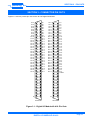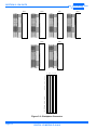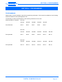
1
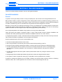
pickering USER MANUAL DIGITAL I/O MODULE (MODEL No. 40-410) Issue 1, Mar 2002 www.pickeringswitch.com pickering ISO 9002 Reg No. FM38792 Pickering Interfaces Ltd. Stephenson Road Clacton-on-Sea CO15 4NL United Kingdom Pickering Interfaces Inc. 966 SW 6th Street Grants Pass Oregon 97526 USA Pickering Interfaces GmbH Buchenstrasse 15 D-77880 Sasbach Germany Pickering Interfaces AB Karl Nordströmsväg 31 432 53 Varberg Sweden Tel: Fax: +44 (0)1255-428141 +44 (0)1255-475058 Tel: Fax: 541 471 0700 541 471 8828 Tel: Fax: +49 7841 66 49 10 +49 7841 66 49 12 Tel: Fax: +46 340-69 06 69 +46 340-69 06 68 E-Mail: [email protected] E-Mail: [email protected] E-Mail: [email protected] E-Mail: [email protected] DIGITAL I/O MODULE 40-410 Page 1 pickering © COPYRIGHT (2002) PICKERING INTERFACES. ALL RIGHTS RESERVED. No part of this publication may be reproduced, transmitted, transcribed, translated or stored in any form, or by any means without the written permission of Pickering Interfaces. Technical details contained within this publication are subject to change without notice. Page ii DIGITAL I/O MODULE 40-410 pickering TECHNICAL SUPPORT For Technical Support please contact Pickering Interfaces either by phone, fax, the website or via e-mail. WARRANTY All products manufactured by Pickering Interfaces are warranted against defective materials and workmanship for a period of two years from the date of delivery to the original purchaser. Any product found to be defective within this period will, at the discretion of Pickering Interfaces be repaired or replaced. Warranty is on a return to factory basis, however, for most systems, the module may be replaced on a module exchange basis. A module will be delivered to the user and the faulty part returned to Pickering Interfaces on receipt. Products serviced and repaired outside of the warranty period are warranted for ninety days. Extended warranty and service are available. Please contact Pickering Interfaces by phone, fax, the website or via e-mail. ENVIRONMENTAL POLICY Pickering Interfaces operates under an environmental management system similar to ISO 14001. Pickering Interfaces strives to fulll all relevant environmental laws and regulations and reduce wastes and releases to the environment. Pickering Interfaces aims to design and operate products in a way that protects the environment and the health and safety of its employees, customers and the public. Pickering Interfaces endeavours to develop and manufacture products that can be produced, distributed, used and recycled, or disposed of, in a safe and environmentally friendly manner. Observe the Electrostatic Sensitive Device Caution detailed in Section 8. Worldwide Technical Support and Product Information http://www.pickeringswitch.com Pickering Interfaces Headquarters Stephenson Road Clacton-on-Sea CO15 4NL United Kingdom Tel: +44 (0)1255-428141 Fax: +44 (0)1255-475058 E-Mail: [email protected] Worldwide Offices Germany Sweden USA Tel: +49 7841 66 49 10 Fax: +49 7841 66 49 12 E-Mail: [email protected] Tel: +46 340-69 06 69 Fax: +46 340-69 06 68 E-Mail: [email protected] Tel: (541) 471 0700 Fax: (541) 471 8828 E-Mail: [email protected] DIGITAL I/O MODULE 40-410 Page iii pickering THIS PAGE INTENTIONALLY BLANK Page iv DIGITAL I/O MODULE 40-410 pickering CONTENTS Copyright Statement .......................................................... ii Technical Support and Warranty....................................... iii Contents (this page)........................................................... v Section 1 Introduction......................................................................... 1.1 Section 2 Installation........................................................................... 2.1 Section 3 Connector Pin Outs............................................................ 3.1 Section 4 Programming ...................................................................... 4.1 Section 5 Fault Diagnosis................................................................... 5.1 Section 6 Technical Specication...................................................... 6.1 Section 7 Parts List ............................................................................. 7.1 Section 8 Caution ................................................................................ 8.1 DIGITAL I/O MODULE 40-410 Page v pickering THIS PAGE INTENTIONALLY BLANK Page vi DIGITAL I/O MODULE 40-410 SECTION 1 - INTRODUCTION pickering SECTION 1 - INTRODUCTION GENERAL The 40-410 Digital I/O Module, which forms part of the System 40 Programmable Relay Switching System, provides 32 bit digital I/O and is used to operate external devices, such as heavy duty relays (power, RF and high voltage types), solenoids, lamps etc., or for interfacing with external logic, e.g. a programmable instrument with a BCD interface. The module is provided in the following congurations: • • 32In/32 Out (TTL O/P) 40-410-001 32In/32 Out (Open Collector O/P) 40-410-002 APPLICATIONS The TTL output version of the module allows interaction with external logic and the Open Collector Transistor version allows operation of external devices with voltages to 50V d.c. and currents to 500mA. Applications include generating control signals, stimulus and sensing status from digital devices. MECHANICAL DESCRIPTION The Digital I/O Module conforms to the 3U height (128mm) Eurocard standard and comprises the following: • • • • • • • CPCI Ejector Handle Front Panel mounted 96-way SCSI 2 Type connector Four 32 bit TTL I/O Drivers Four 32 bit Open Collector I/O Drivers Compact PCI backplane connector PCI Bridge (U1) Control Logic The front panel is secured to the PCB by two M2.5 x 6mm pan-head posi-drive screws. DIGITAL I/O MODULE 40-410 Page 1.1 SECTION 1 - INTRODUCTION pickering FUNCTIONAL DESCRIPTION A functional block diagram is provided in Figure 1.1. The Module is powered by the +5V supply from the PXI backplane via Compact PCI connector J1. The interface to the user test equipment is via the front panel mounted 96-way SCSI type connector, J2. The module comprises Open Collector output drivers U16 to U19, TTL input/output drivers U8 to U15, control logic U3 to U4, conguration EEPROMS U2 and U7 and PCI Bridge U1. The module conguration, i.e. Open collector output or TTL output, is determined by data stored in EEPROM U7. U16 to U19 and U8 to U15 are addressed by PCI bridge U1 to output the required signal. PCI Bridge U1 is congured by EEPROM U2. 96-WAY SCSI TYPE CONNECTOR J2 COMPACT PCI BUS CONNECTOR J1 OPEN COLLECTOR OUTPUTS U16 to U19 CONTROL LOGIC U3, U4, U5, U6 TTL I/O U8 to U15 MODULE CONFIGURATION U7 PCI BRIDGE U1 TERMINATING RESISTORS R4 TO R15 +5V PCI BRIDGE CONFIGURATION U2 0V Figure 1.1 - Digital I/O Module 40-410: Functional Block Diagram Page 1.2 DIGITAL I/O MODULE 40-410 SECTION 2 - INSTALLATION pickering SECTION 2 - INSTALLATION CAUTION Electrostatic discharge can damage the components on the module. To avoid such damage in handling the board, touch the anti-static bag to a metal part of the chassis before removing the board from the bag. The module should be installed in accordance with the following procedure: 1. Ensure that the system is turned OFF but still connected to mains so that it remains grounded. 2. Choose an appropriate slot in the rack (refer to the slot address information in Section 4). 3. Remove the slot cover for the chosen slot. 4. Ensure that the injector/ejector handle is in its downward position. Align the module with the card guides on the top and bottom of the slot. CAUTION Do not raise the injector/ejector handle whilst inserting the module. The module will not insert properly unless the handle is in its downward position. 5. Hold the handle whilst slowly sliding the module into the card guides until the handle catches on the injector/ejector rail (refer to Figure 2.1). Figure 2.1 - Installing the module into a PXI Chassis DIGITAL I/O MODULE 40-410 Page 2.1 SECTION 2 - INSTALLATION pickering 6. Raise the injector/ejector handle until the module rmly seats into the backplane. The front panel of the module should be ush with the front panel of the chassis. 7. Screw the front panel of the module to the front panel mounting rail. 8. Power-up the system as follows: a. For a system comprising a PC and one rack, power up the rack before powering up the PC. b. For a system comprising more than one rack, turn ON the last rack in the system followed by the penultimate, etc, and nally turn ON the PC. NOTES 1. In a MXI-3 arrangement the entire system must be powered down when any change is made to its card complement. 2. There is a relationship between physical slot-numbers and logical bus/slot values. 3. The logical bus values are dynamic (eg. if a PXI-MXI-3 card is repositioned in a chassis). 4. Each module requires a Software driver. These are available on the Pickering Interfaces website at www.pickeringswitch.com. Page 2.2 DIGITAL I/O MODULE 40-410 SECTION 2 - PIN OUTS pickering SECTION 3 - CONNECTOR PIN OUTS Figures 3.1 and 3.2 provide pin outs for the 40-410 Digital I/O Module. IN 1 OUT 1 OUT 2 49 1 50 2 OUT 3 OUT 4 51 3 52 4 IN 2 IN 3 IN 4 OUT 5 OUT 6 53 5 54 6 IN 5 IN 6 OUT 7 OUT 8 55 7 56 8 IN 7 IN 8 OUT 9 OUT 10 OUT 11 OUT 12 57 9 58 10 59 11 60 12 IN 9 IN 10 OUT 13 OUT 14 61 13 62 14 OUT 15 OUT 16 OUT 17 63 15 64 16 65 17 66 18 67 19 OUT 18 OUT 19 OUT 20 OUT 21 OUT 22 OUT 23 OUT 24 OUT 25 OUT 26 OUT 27 OUT 28 OUT 29 OUT 30 OUT 31 OUT 32 68 20 69 21 70 22 71 23 72 24 73 25 74 26 75 27 76 28 77 29 78 30 79 31 80 32 81 33 82 34 83 35 IN 11 IN 12 IN 13 IN 14 IN 15 IN 16 IN 17 IN 18 IN 19 IN 20 IN 21 IN 22 IN 23 IN 24 IN 25 IN 26 IN 27 IN 28 IN 29 IN 30 IN 31 IN 32 OUT 1 OUT 2 49 1 50 2 IN 1 IN 2 OUT 3 OUT 4 51 3 52 4 IN 3 OUT 5 OUT 6 OUT 7 OUT 8 OUT 9 53 54 55 56 57 OUT 10 58 10 OUT 11 OUT 12 59 11 60 12 OUT 13 OUT 14 61 13 62 14 OUT 15 OUT 16 OUT 17 OUT 18 OUT 19 OUT 20 OUT 21 OUT 22 OUT 23 OUT 24 OUT 25 OUT 26 OUT 27 OUT 28 OUT 29 OUT 30 63 15 64 16 65 17 66 18 67 19 68 20 69 21 70 22 71 23 72 24 73 25 74 26 75 27 76 28 77 29 78 30 OUT 31 OUT 32 79 31 80 32 81 33 82 34 83 35 IN 16 IN 17 IN 18 IN 19 IN 20 IN 21 IN 22 IN 23 IN 24 IN 25 IN 26 IN 27 IN 28 IN 29 IN 30 IN 31 IN 32 VCOMM 89 41 90 42 89 41 90 42 91 43 92 44 91 43 92 44 93 45 94 46 40-410-001 IN 13 IN 14 IN 15 85 37 86 38 87 39 88 40 86 38 87 39 88 40 95 47 96 48 IN 4 IN 5 IN 6 IN 7 IN 8 IN 9 IN 10 IN 11 IN 12 84 36 84 36 85 37 0V 5 6 7 8 9 0V 93 45 94 46 95 47 96 48 40-410-002 Figure 3.1 - Digital I/O Module 40-410: Pin Outs DIGITAL I/O MODULE 40-410 Page 2.1 SECTION 2 - PIN OUTS pickering ROW A ROW B ROW C 5V 1 n/c 1 n/c 1 n/c 1 AD1 2 +5V 2 n/c 2 AD0 2 n/c 3 AD4 3 AD3 3 +5V 3 AD7 4 Gnd 4 n/c 4 AD6 4 n/c 5 AD9 5 AD8 5 n/c 5 AD12 6 Gnd 6 n/c 6 AD11 6 n/c 7 AD15 7 AD14 7 Gnd 7 SERR# 8 Gnd 8 n/c 8 PAR 8 n/c 9 n/c 9 n/c 9 Gnd 9 DEVSEL# 10 Gnd 10 n/c 10 STOP# 10 n/c 11 FRAME# 11 IRDY# 11 Gnd 11 AD18 12 AD17 12 AD16 12 Gnd 12 AD21 13 Gnd 13 n/c 13 AD20 13 CBE3# 14 IDSEL 14 AD23 14 Gnd 14 AD26 15 Gnd 15 n/c 15 AD25 15 AD30 16 AD29 16 AD28 16 Gnd 16 n/c 17 Gnd 17 n/c 17 CLK 17 n/c 18 n/c 18 RST# 18 Gnd 18 n/c 19 Gnd 19 n/c 19 n/c 19 n/c 20 n/c 20 n/c 20 5V 20 n/c 21 +5V 21 n/c 21 n/c 21 5V 22 n/c 22 n/c 22 n/c 22 ROW E ROW F +5V 1 Gnd 1 n/c 2 Gnd 2 AD2 3 Gnd 3 AD5 4 Gnd 4 C/CB0# 5 Gnd 5 AD10 6 Gnd 6 AD13 7 Gnd 7 CBE1# 8 Gnd 8 PERR# 9 Gnd 9 LOCK# 10 Gnd 10 TRDY# 11 Gnd 11 CBE2# 12 Gnd 12 AD19 13 Gnd 13 AD22 14 Gnd 14 AD24 15 Gnd 15 AD27 16 Gnd 16 AD31 17 Gnd 17 n/c 18 Gnd 18 n/c 19 Gnd 19 n/c 20 Gnd 20 n/c 21 Gnd 21 5V 22 Gnd 22 F E D C B A 1 2 3 4 5 6 7 8 9 10 11 12 13 14 15 16 17 18 19 20 21 22 Figure 3.2 - Backplane Connector Page 2.2 ROW D DIGITAL I/O MODULE 40-410 SECTION 4 - PROGRAMMING pickering SECTION 4 - PROGRAMMING PROGRAMMING Please refer to the PXI Software manual for programming information. This manual is available on the Pickering Interfaces website at www.pickeringswitch.com. The following provides slot addresses for the Pickering Interfaces 19 inch rack: First three slots for controller Front Panel No. Bus 02h Slot 0fh Slot 0eh Slot 0dh Slot 0bh Slot 0ah Slot 2 Slot 3 Slot 4 Slot 5 Slot 6 Slot 0fh Slot 0eh Slot 0dh Slot 0bh Slot 0ah Slot 09h Slot 7 Slot 8 Slot 9 Slot 10 Slot 11 Slot 12 Slot 0fh Slot 0eh Slot 0dh Slot 0ch Slot 0bh Slot 0ah Slot 13 Slot 14 Slot 15 Slot 16 Slot 17 Slot 18 Bus 03h Front panel No. Bus 04h Front panel No. DIGITAL I/O MODULE 40-410 Page 4.1 SECTION 4 - PROGRAMMING pickering THIS PAGE INTENTIONALLY BLANK Page 4.2 DIGITAL I/O MODULE 40-410 SECTION 5 - FAILURE DIAGNOSIS pickering SECTION 5 - FAILURE DIAGNOSIS There is no self-test facility provided on the 40-410 Digital I/O Module. FAILURE DIAGNOSIS General In general, PCI Plug and Play functions correctly in desktop PCs, but the same cannot be guaranteed for PXI. Many problems relate to system conguration issues. Although MXI-3 itself is a reliable technology, problems can arise by making it possible to attach a far greater number of PCI devices to a desktop PC than the BIOS is designed to handle. The BIOS may also be confused when card positions are interchanged in the chassis. Because, in some cases, the underlying technology of PXI is not understood it is sometimes difcult to make sense of apparently bizarre system behaviour. For instance in a borderline situation, adding a new card to a functioning system can cause one of the original cards to stop working (by starving it of resources). A lot of reported problems are related to large systems, so many points relate to them. There also arises the problem of software conict, in some cases another vendors’ software installation has overwritten the existing Pickering Interfaces WinDriver installation with their own, older version). In a signicant proportion of cases, cards returned to Pickering Interfaces as faulty are found to be fully functional. This is another indication of problems in the host system environment. Some fundamental issues of PXI which cause problems are: • • • • the need to install software drivers for the cards • in a MXI-3 arrangement the entire system must be powered down when any change is made to it’s card complement • • the apparently bizarre relationship between physical slot-numbers and logical bus/slot values when using PCI-MXI-3, the need to power up PXI chassis before powering up the PC the need to power up daisy-chained PXI chassis in reverse order so that resources are detected properly in a MXI-3 arrangement the PXI chassis must never be switched off while the host PC is operating (being connected like an ordinary peripheral, such as a printer or a GPIB instrument, they expect it to behave like one) the ‘dynamic’ nature of logical bus values (eg. if a PXI-MXI-3 card is repositioned in a chassis) It should be noted that programs such as PILMon, PILDemo and PILCfg obtain exclusive access to Pickering Interfaces cards, and no other application can access the cards until those programs are quit. DIGITAL I/O MODULE 40-410 Page 5.1 SECTION 5 - FAILURE DIAGNOSIS pickering USEFUL HARDWARE INFORMATION Does the system use an embedded controller, or PCI-MXI-3 connection to a desktop PC? An embedded controller can be expected to have a “PXI-suitable” BIOS. A standard desktop PC (or even an industrial PC that’s tailored for PCI applications) may not. If PCI-MXI-3: • • who is the PC manufacturer? what BIOS does it use? Some BIOSs cannot map more than 80 memory windows. A typical result is that when the number of cards in the system is increased beyond some point, additional cards do not function properly (or at all), or some cards that did function correctly cease to do so. The failure point is dependent upon the precise demands of motherboard devices and the installed cards. Because a typical card uses 2 windows, failure might be expected at around 35 cards. Some designs make excessive use of memory windows (upto 5 windows per card) and the problem can occur with as few as 14 such cards. What CPU manufacturer, type and clock speed? There are no known problems associated with particular CPU manufacturers, types, or clock speed. But with clock speeds continually rising, there is always a fear that some speed-related bug will manifest itself. What PXI chassis is/are in use in the system? Assuming the chassis type is recognised, the total slot-count of the system can be deduced, and the number of PCI buses involved. If multiple chassis are in use, what connection topology is being employed (star, daisy-chain, or some combination)? Theoretically it should not matter how the system is connected. But the overall topology determines the enumeration order of the system’s PCI buses, and consequently the physical location at which the BIOS or OS may run out of resources to allocate to cards. What is the total slot-count of the system? May be deduced from the chassis information, assuming the types are recognised. If not, the slot-count indicates the number of PCI buses present. How many slots are occupied? The installed card-count gives a rough indication of the total demand that may be placed on system resources. What Pickering Interfaces cards are installed? The resource requirement of the Pickering Interfaces cards tted in the rack should be determined. What other manufacturer’s cards are installed? There are no known cases of conict with particular card types from other manufacturers. PCI PnP should guarantee that all devices are assigned non-conicting resources. Any conicts that do occur can only be blamed on the BIOS (and/or PnP OS) for getting it wrong. However in some cases it appears that the BIOS may have been provoked into making an error by the combination of resources it was being asked to assign within a single bus segment. Page 5.2 DIGITAL I/O MODULE 40-410 SECTION 5 - FAILURE DIAGNOSIS pickering Have cards been moved around in the system, or has MXI-3 connection topology been changed? The PC’s BIOS holds a picture of the system’s conguration and resource assignments in NVRAM. If the conguration is altered the BIOS should re-build its picture accordingly; but in complex congurations some BIOSs corrupt. To correct this problem in a PCI-MXI-3 arrangement: 1. 2. 3. 4. Turn off the PC and all PXI chassis. Turn on the PC only and allow it to boot with all PXI devices ‘dead’. Shut down and switch off the PC. Wait for approximately ve seconds. Turn on the PXI chassis and then the PC. This should cause the BIOS to create a ‘clean’ picture. Are there any ‘oating’ MXI-3 links? Some systems have a ‘oating’ PXI-MXI-3 card installed (one that will ultimately connect to another chassis, or is connected to a chassis that is unpowered). In some cases a oating MXI-3 link will hang the computer at boot-time, or cause random system crashes. From a system viewpoint it represents “half-a-bridge” and should be avoided. What is the exact logical PCIbus conguration of the system? This information can be obtained using the following: WinDriver PCI_Dump utility The Catalyst Hot-swap utility Windows Device Manager which can print “All devices and system summary” information, but it only shows what resources have actually been assigned, rather than those the cards might have requested. USEFUL SOFTWARE INFORMATION Has the Pickering software been properly installed? The rst-generation driver Pilpxi.dll and utilities that rely on it such as PILMon, PILDemo and PILCfg require WinDriver installed in the system. The VISA driver Pipx40.dll relies on NI-VISA being installed. When Pickering cards were installed, was the appropriate driver le used? For the rst-generation driver Pilpxi.dll, Plug and Play installation using Pilpxi.inf places the cards in the Device Manager class “Pickering Interfaces PXI”. Cards will still function if installed as “Unknown” (ie. without using Pilpxi.inf). Cards installed using Pilpxi.inf or as “Unknown” are not registered with VISA, and so are not operable by the Pipx40.dll driver or utilities such as MAX. To overcome this, rst remove the affected card(s) in Device Manager. Install the latest System 40 software release, then restart. The cards should now re-install, appearing in the Device Manager class “Pickering Interfaces PXI VISA”, and will be accessible to Pipx40.dll etc. Registering the cards with VISA does not prevent Pilpxi.dll from accessing the cards. Which Pickering driver is in use (Pilpxi.dll or Pipx40.dll)? The rst-generation driver Pilpxi.dll is not reliant on NI-VISA and is usable by customers who do not have it. PXI support in NI-VISA is currently an NI extension to the VISA specication. PXI support is not guaranteed in other vendors’ VISA distributions. The VISA driver Pipx40.dll will become available soon. At some later time Pipx40ivi.dll will take over from it (though retaining all ‘legacy’ VISA functionality of Pipx40.dll). DIGITAL I/O MODULE 40-410 Page 5.3 SECTION 5 - FAILURE DIAGNOSIS pickering What is the version of the Pickering driver? Use of the latest available version is always recommended, because: • • new card types may need revised driver features to support them recently-purchased cards may not be recognised by old driver releases (because Subsystem IDs have changed versions of Pilpxi.dll prior to 1.36 will not recognise the new IDs) PICKERING INFORMATION Are all installed cards detected by PILMon? If not, the likelihood is that either: • • Pilpxi.dll is too old, and cannot recognise the missing card(s) there is a problem with allocating system resources, and the missing card(s) have not received their proper assignments Are all cards’ attributes shown correctly by the PILMon “LS” command, and all status values = 0x00000000? Erroneous card descriptions from “LS” are largely due to the program not being rigorous enough, and will invariably be accompanied by non-zero status values. Non-zero status values indicate faulty card hardware or communication problems. Page 5.4 DIGITAL I/O MODULE 40-410 SECTION 6 - SPECIFICATION pickering SECTION 6 - SPECIFICATION ENVIRONMENTAL Operating Temperature: 0°C to 50°C. Storage Temperature: -20°C to 75°C. Humidity 95% non condensing. POWER REQUIREMENT Power consumption from the 5V backplane supply is as follows: 0.9W + 0.25W from User 5V. POWER SUPPLY Choice of all four PXI system voltages (+3.3VDC, +5VDC ±12VDC) up to 1amp each (within the overall limit of the power supply). The power supplies are all fused at 1A as standard (however maximum fuse value can be changed to 8A for 3,3Vd.c. and 5A for 5Vd.c.). DIMENSIONS Single slot 3U PXI (CompactPCI card). MATING CONNECTORS 96 Way SCSI 2 Female Connector PXI bus via 32 bit P1/J1 backplane connector. GENERAL BREADBOARD DETAILS Square pad and DIP construction areas. Approximately 652cm (10 sq inches) of prototype area. 0.1” grid spacing. Maximum Component Height: 13mm Maximum Lead Length Below PCB: 2mm TTL OUTPUT DRIVER Maximum drive 15 TTL inputs Max Voltage 7V Max Current Drive Sink 8mA, Source 0.4mA Operate/Release Time < 1ms OPEN COLLECTOR TRANSISTOR Driver I.C. ULN2803LW, Open Collector Driver Maximum Standoff Volts 50V Max Power per O/P 1.0W Max Power per byte 1.6W Max Current Drive 500mA. Operate/Release Time < 1ms DIGITAL I/O MODULE 40-410 Page 6.1 SECTION 6 - SPECIFICATION pickering THIS PAGE INTENTIONALLY BLANK Page 6.2 DIGITAL I/O MODULE 40-410 SECTION 7 - PARTS LIST pickering SECTION 7 - PARTS LIST The following pages provide a parts list and component layout diagram for the Digital I/O Module 40-410. DIGITAL I/O MODULE 40-410 Page 7.1 SECTION 7 - PARTS LIST pickering Table 7.1 provides a parts list and Figure 7.1 a component layout diagram for the 40-410 Digital I/O Module TABLE 7.1 - Digital I/O Module 40-410 Parts List PCB Location Part Description Quantity R1, R2, R16 to R23 C/RS/079 RESISTOR N/W 4 x 10k 1206 R3 C/RS/085 RESISTOR 10k 0805 R4 to R15 C/RS/102 RESISTOR N/W 4 x 10R 1206 12 RL1 to RL32, RL49 C/RL/ 110/111 33 RL33 to RL48, RL50 C/RL/015 108-1-C 17 C2 to C23, C25, C27, C29 t0 C34 C/CP/034 CAPACITOR 100nF 0603 30 C1 C24, C26, C28 C/CP/024 CAPACITOR 10uF TANT SMD 4 Fuse 3.3V 1A 1 Fuse 5V 1A 1 Fuse +12V 1A 1 Fuse -12V 1A 1 C/CN/355 cPCI CONNECTOR 1 C/MS/071 FEMALE CODING KEY, BRILLIANT BLUE, V 1 J2 C/CP/379 SCSI3 68 PIN 1 U1 C/IC/098 PCI9050 PQFP 1 U2 C/IC/099 93CS46 DIP 1 C/IC/035 8 PIN DIP SKT 1 U3 C/IC/056 7705 SOP 1 U4 C/IC/087 74HCT32 SOP 1 U5 C/IC/100 74HCT273 SOP 1 U6 C/IC/101 74HCT244 SOP 1 U7 C/IC/090 93C56 SOP 1 U16 to U19 C/IC/092 UCN2803LW 4 U8 to U11 C/IC/102 74ACT273 SOP 4 J1 Page 7.2 Pickering Interfaces Part Number DIGITAL I/O MODULE 40-410 10 1 SECTION 7 - PARTS LIST 32 C34 C33 U19 C32 U18 C31 U17 C20 U16 C21 U8 C22 U9 C23 U10 1 17 32 TTL OUTPUTS pickering U11 1 32 OPEN COLLECTOR OUTPUTS +12V 16 -12V U12 5V U13 U14 1 U15 32 17 32 TTL INPUTS 3.3V Gnd +12V J2 C17 C16 -12V C18 U3 5V C19 C15 R2 C14 U4 3.3V Gnd U6 C13 U7 C8 5V U2 U20 R21 C9 C10 R3 R4 R5 R6 R8 R9 Gnd R10 U1 +12V R12 C5 R13 3.3V C4 R14 +12V C24 +12V C26 -12V -12V C3 R15 C2 C1 C25 C28 3.3V 5V C27 UNCOMMITED POWER RAILS UNCOMMITED POWER RAILS 3.3V C29 UNCOMMITED POWER RAILS UNCOMMITED POWER RAILS FUSES C30 GND RAILS J1 R11 -12V Gnd 32 R7 C6 3.3V 5V 16 R20 R19 R18 R17 R16 C12 +12V -12V R22 U7 C11 C7 R23 R1 Figure 7.1 - Digital I/O Module 40-410: Component Layout DIGITAL I/O MODULE 40-410 Page 7.3 SECTION 7 - PARTS LIST pickering THIS PAGE INTENTIONALLY BLANK Page 7.4 DIGITAL I/O MODULE 40-410 pickering SECTION 8 - CAUTION CAUTION Handling of Electrostatic-Sensitive Semiconductor Devices Certain semiconductor devices used in the equipment are liable to damage due to static voltage. Observe the following precautions when handling these devices in their unterminated state, or sub-units containing these devices: (1) Persons removing sub-units from an equipment using these devices must be earthed by a wrist strap and a resistor at the point provided on the equipment. (2) Soldering irons used during the repair operations must be low voltage types with earthed tips and isolated from the mains voltage by a double insulated transformer. (3) Outer clothing worn must be unable to generate static charges. (4) Printed Circuit Boards (PCBs) fitted with these devices must be stored and transported in anti-static bags. DIGITAL I/O MODULE 40-410 Page 8.1 pickering THIS PAGE INTENTIONALLY BLANK Page 8.2 DIGITAL I/O MODULE 40-410