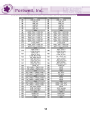
1
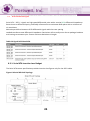
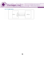
QSEVEN Design Guide For Designing QSEVEN Carrier boards Revision 2.0 Revision History Rev. 0.1 Date 2009/3/1 Author Darwin 2.0 2014/08/20 Ian Changes Initial Release Update to Rev. 2,0, Update PQ7-M106 Design info Update Input Power Sequencing info Table of Contents 1. 2. 3. 4. 5. QSEVEN™ Specification ................................................................................... 5 QSEVEN™ Connector ....................................................................................... 6 QSEVEN™ Feature Overview ............................................................................. 8 QSEVEN™ Connector Pin out ............................................................................ 9 QSEVEN™ Carrier Board Design ....................................................................... 13 5-1. PCB Design Rules .............................................................................. 13 5-2. Trace-Impedance Considerations ...................................................... 13 6. Signal Descriptions ...................................................................................... 16 6-1. PCI Express Interface Signal............................................................... 17 6-1-1. PCI Express Insertion Loss Budget.......................................... 18 6-2. Gigabit Ethernet Signals .................................................................... 21 6-2-1. Gigabit Ethernet Insertion Loss Budget .................................. 22 6-2-2. LAN Component Placement .................................................. 23 6-3. Serial ATA Interface Signals ............................................................... 24 6-3-1. Serial ATA Insertion Loss Budget............................................ 24 6-4. USB Interface Signals ........................................................................ 26 6-4-1. USB Client ............................................. 錯誤! 尚未定義書籤。 6-5. SDIO Interface Signals ....................................................................... 29 6-6. High Definition Audio Signals ............................................................ 37 6-6-1. HDA Placement and Routing Guidelines ................................ 37 6-7. LVDS Flat Panel Signal ..................................................................... 39 6-7-1. LVDS Implementation Guidelines ........................................... 41 6-8. DisplayPort Interface Signals ............................................................. 42 6-9. HDMI Interface Signals ..................................................................... 44 6-10. LPC interface Signal....................................................................... 45 6-11. CAN Bus Interface Signals ............................................................. 45 6-12. SPI Interface Signals ...................................................................... 46 6-13. UART Interface Signals .................................................................. 46 6-14. Input power pin ............................................................................ 46 6-15. Power control signal ..................................................................... 47 6-16. Power Management signals .......................................................... 47 6-17. Miscellaneous Signals ................................................................... 48 6-18. Manufacturing Signals .................................................................. 49 6-19. Thermal Management Signals ....................................................... 50 6-20. Fan Control Implementation ......................................................... 50 7. Input Power Requirements ........................................................................... 51 7-1. Input Power Sequencing ................................................................... 52 8. General Considerations for Differential Signal .................................................. 53 I Figure 2-1 MXM connector. .................................................................................... 6 Figure 2-2 Overall Height including Heat-spreader of the Qseven® Module.............. 7 Figure 4-1 Connector Pin out Description. .............................................................. 9 Figure 5-1 Microstrip Diagram. ............................................................................. 14 Figure 5-2 Stripline Diagram. ................................................................................ 14 Figure 5-3 Differential Trace Dimension Terminology. ........................................... 14 Figure 5-4 Trace Spacing vs Trace Width Examples. ............................................... 15 Figure 6-1 PCI Express Link Topology 1. ................................................................. 18 Figure 6-2 PCI Express Link Topology 2. ................................................................. 19 Figure 6-3 Gigabit Ethernet Link Topology. ............................................................ 22 Figure 6-4 Serial ATA Link Topology. ...................................................................... 24 Figure 6-5 USB 2.0 Link Topology .......................................................................... 28 Figure 6-6 SD and SDIO Protocol Interface Block Diagram. .................................... 31 Figure 6-7 SD/SDIO Protocol Clock/DATA/CMD Routing Topology. ......................... 32 Figure 6-8 HPD Passgate Design Recommendation. ............................................... 43 Figure 7-1 Input Power Sequencing. ..................................... 錯誤! 尚未定義書籤。 Figure 8-1 Symmetrical and Non-Symmetrical Routing.......................................... 55 Figure 8-2 Trace Edge to Reference Plane Guidance. ............................................. 55 Figure 8-3 Length Matching Example. ................................................................... 56 Figure 8-4 Serpentining Example. ...................................................................... 56 Figure 8-5 Acceptable Bends vs. Tight Bends Example. ......................................... 57 Figure 8-6 Via Pair Placement. ............................................................................. 57 Figure 8-7 Via Pair Placement. ............................................................................. 58 II Table 2-1 MXM Connector. ..................................................................................... 6 Table 3-1 QSEVEN™ Supported Features. ................................................................ 8 Table 6-1 Signal Terminology. ............................................................................... 16 Table 6-2 Signal Definition PCI Express. ................................................................ 17 Table 6-3 Carrier Board PCI Express Insertion Loss Budget. .................................... 19 Table 6-4 Signal Definition Ethernet. .................................................................... 21 Table 6-5 Signal Definition Ethernet. .................................................................... 22 Table 6-6 Signal Definition SATA. .......................................................................... 24 Table 6-7 SATA Gen 1 Loss Budget Allocation. ....................................................... 25 Table 6-8 SATA Gen2 Loss Budget Allocation. ........................................................ 25 Table 6-9 Signal Definition USB. ........................................................................... 27 Table 6-10 Signal Definition Ethernet.................................................................... 28 Table 6-11 Signal Definition SDIO. ........................................................................ 29 Table 6-12 Signal Definition HAD. ......................................................................... 37 Table 6-13 Signal Definition LVDS. ........................................................................ 40 Table 6-14 Signal Definition DisplayPort. .............................................................. 42 Table 6-15 Signal Definition HDMI. ....................................................................... 44 Table 6-16 Signal Definition LPC. .......................................................................... 45 Table 6-17 Signal Definition CAN Bus. ................................................................... 45 Table 6-18 Signal Definition SPI. ........................................................................... 46 Table 6-19 Signal Definition of UART. .................................................................... 46 Table 6-20 Signal Definition Input Power. ............................................................. 46 Table 6-21 Signal Definition Power Control. .......................................................... 47 Table 6-22 Signal Definition Power Management. ................................................. 47 Table 6-23 Signal Definition Miscellaneous. .......................................................... 48 Table 6-24 Signal Definition Manufacturing. ......................................................... 49 Table 6-25 Signal Definition Miscellaneous. .......................................................... 50 Table 6-26 Signal Definition Fan Control. .............................................................. 50 Table 7-1 Input Power Characteristics. .................................................................. 51 Table 7-2 Input Power Sequencing. ...................................................................... 52 III 4 1. QSEVEN™ Specification PQ7 series Specification defines requirements for highly integrated compact moduleswith standard I/O interfaces and connections. Key capabilities defined in the PQ7 specification include support for: PCI Express Serial ATA USB 2.0 USB 3.0 DisplayPort™, TMDS Secure Digital I/O interface LPC interface Gigabit Ethernet LVDS Display Interface High Definition Digital Audio (HDA) Intergrated Interchip Sound (I2S) PQ7 series have a standardized form factor of 70mm x 70mm and have specified pin outs based on the high speed MXM system connector. 5 2. QSEVEN™ Connector PQ7 series utilizes a 230-pin card-edge connector. The MXM connector accommodates various connector heights for different carrier board application needs. This specification suggests two connector heights, 7.8mm and 7.5mm. Figure 2-1 MXM connector. The connectors mentioned in Table 2-1 are only a partial list of what is offered by the manufacturers. Table 2-1 MXM Connector. The components located on the top side of the module are up to 5.5mm high. The bottom components have a maximum height of 2.5mm while the standard distance between the standard MXM connector on the carrier board and the PQ7 series module is 2.7mm. When using the standard MXM connector, with an overall height of 5.5mm, carrier board component placement below the PQ7 series module is not permitted. 6 If it is necessary to place carrier board components below the PQ7 series module, then a MXM connector with an overall height of 7.8mm must be used and no carrier board component can exceed a maximum height of 2.5mm. The heatspreader offered for PQ7 series modules acts as a thermal coupling device and is not heat sink. Heat dissipation devices such as a heat sink with fan or heat pipe may need to be connected to the heat spreader. The dissipation of heat will fluctuate between different CPU boards. Refer to the PQ7 series module user's manual for heat spreader dimensions and specifications. The standoff for the heat spreader and carrier board must not exceed 5.6 mm overall external diameters. It ensures that the standoff contact-area does not exceed the defined mounting hole footprint on the PQ7 series module. The screw that is to be used for mounting must be a metric thread M2.5 DIN7985 / ISO7045. PQ7 series modules are defined to feature ultra low power CPU and chipset solutions with an ultra low “ Thermal Design Power ” (TDP). The modules power consumption not exceeds 12W. Figure 2-2 Overall Height including Heat-spreader of the Qseven® Module. 7 3. QSEVEN™ Feature Overview The Qseven mandatory and optional feature as Table 3-1 shows the minimum、maximum and PQ7 series configuration of the feature set. Table 3-1 QSEVEN™ Supported Features. Note: Please refer to PQ7 series modules’ user manual for detail information. 8 4. QSEVEN™ Connector Pin out Figure 4-1 Connectors Pin out Description. 9 10 11 Note: Please refer to PQ7 series modules’ user manual for detail information. 12 5. QSEVEN™ Carrier Board Design 5-1. PCB Design Rules The PQ7 series Specification provides a rich set of modern, high-speed differential serial interfaces. Designing PQ7 series Carrier Boards must be followed the certain design rules. The most important design rule is route high-speed serial interfaces as differential pairs.The two lines in the pair must be length-matched and should have uniform edge-to-edge spacing. They should have a minimum of layer changes. If they do change layers, both lines in the pair should change. The preferred reference plane for the high-speed pairs is a single, continuous GND plane. If the differential pair is referenced to a power plane, avoid routing the pair across a power-plane split. 5-2. Trace-Impedance Considerations Most high-speed interfaces used in a QSEVEN™ design for a Carrier Board are differential pairs that need a well-defined and consistent differential and single-ended impedance. he differential pairs should be edge-coupled There are two basic structures used for high-speed differential and single-ended signals. The first is “microstrip”, in which a trace or trace pair is referenced to a single ground or power plane. The outer layers of multi-layer PCBs are microstrips. A diagram of a microstrip cross section is shown in Figure 5-1 below. The second structure is “stripline” in which a trace or pair of traces is sandwiched between two reference planes, as shown in Figure 5-2 below. If the traces are exactly halfway between the reference planes, then the stripline is said to be symmetric or balanced. Usually the traces are a lot closer to one of the planes than the other. Inner layer traces on multi-layer PCBs are usually asymmetric striplines. Before proceeding with a Carrier Board layout, designers should decide on a PCB stack-up and on trace parameters, primarily the trace-width and differential-pair spacing. It is quite harder to change the differential impedance of a trace pair after layout work is done than it is to change the impedance of a single-ended signal. It is more important for the PCB designer and the Project Engineer to determine the routing parameters for differential pairs ahead of time. 13 Figure 5-1 Microstrip Diagram. NOTE: The trace spacing vary from one signal group to the other. Each signal group’s values are specified in their respective sections within this design guide. Figure 5-2 Stripline Diagram. NOTE: The trace spacing vary from one signal group to the other. Each signal group’s values are specified in their respective sections within this design guide. Figure 5-3 Differential Trace Dimension Terminology. 14 Figure 5-4 Trace Spacing vs Trace Width Examples. 15 6. Signal Descriptions The “#” symbol at the end of the signal name indicates that the active, or asserted state, occurs when the signal is at a low voltage level. When “#” is not present, the signal is asserted when at a high voltage level. Differential pairs are indicated by trailing‘+’ and ‘-’ signs for the positive or negative signal. The following terminology is used to describe the signals types in the I/O columns for the tables located below. Table 6-1 Signal Terminology. 16 6-1. PCI Express Interface Signal According to the PCI Express Base Specification Revision 1.1, a total available interconnect loss budget of 13.2 dB is allowed between the PCI Express host device on the Qseven® CPU module and the PCI Express device on the carrier board, ExpressCard or PCI Express add-in card. The specifications contained herein apply to all high-speed signals of each interface width definition. The signaling rate for encoded data is 2.5 Gigabit transfers/s and the signaling is point-to-point. PCI Express (PCIe) signals are high-speed differential pairs with a nominal 85Ω differential impedance. Route them as differential pairs, preferably referenced to a continuous GND plane with a minimum of via transitions. Table 6-2 Signal Definition PCI Express. PCIe pairs need to be length-matched within a given pair, but the different pairs do not need to be matched. The transmit pairs are designated as PCIE0_TX+ and PCIE0_TX- thru PCIE1_TX+ and PCIE1_TX-. Transmit in this context means that the signals are transmitted out of the Module. No coupling capacitors are needed on Carrier Board PCIe transmit lines. The coupling caps are located on the Module. The receive pairs are designated PCIE0_RX+ and PCIE0_RX- thru PCIE1_RX+ and PCIE1_RX-. Receive in this context means that the signals are received by the Module. Coupling capacitors are needed on the Carrier Board on these lines if the PCIe target device is down on the Carrier Board. Locate the coupling capacitors near the transmit pins of the Carrier Board’s PCIe target device. If the PCIe target device is on a slot card, then no coupling caps are needed on the lines on the Carrier Board because the coupling caps will be on the slot card. 17 6-1-1. PCI Express Insertion Loss Budget Figure 6-1 PCI Express Link Topology 1. 18 Figure 6-2 PCI Express Link Topology 2. Table 6-3 Carrier Board PCI Express Insertion Loss Budget. The trace lengths presented in Table are based on the following assumptions: Typical damping of the PCB trace of 0.35dB/inch @ 1,25GHz (common value for FR-4 based material) The RX path budget includes the additional damping of the DC decoupling capacitors and 2 additional vias for connecting the decoupling capacitors Maximum 2 vias per trace for a RX path and maximum 4 vias per trace for a TX path on the connection from the the Qseven ® connector on the Qseven ® carrier board to an onboard device Maximum 2 vias per trace for a RX path and maximum 2 vias per trace for a TX path on the connection from the Qseven ® connector on the Qseven ® carrier board to a PCI Express extension socket that is compliant to the properties defined 19 in the PCI Express Card Electromechanical Specification (this includes standard PCI Express cards as well as ExpressCards). Trace routing is implemented according to the design rules for high speed differential traces. The values in Table above are derived from a signal integrity simulation and reflect a worst case scenario. Designers that face the necessity to deviate from the given values have to conduct a suitable signal integrity simulation to guarantee compliance to the PQ7 series specification and the underlying PCI Express specification. For USB3.0, HDMI and DisplayPort interface signals the description offered in this section is also applicable. 20 6-2. Gigabit Ethernet Signals The LAN port defines to support a 10/100 Megabits per second or Gigabit Ethernet. The Module Specification specifies that LAN magnetics must reside on the Carrier Board, not on the Module. The LAN interface consists of four differential pair signals, designated as GBE_MDI0+/- thru GBE_MDI3+/-. Additionally, there are four single-ended signals that provide link-status information, along with a reference voltage for the magnetics center tap. Route LAN differential pairs with 100Ω differential impedance and 50Ω, single-end impedance. Table 6-4 Signal Definition Ethernet. 21 6-2-1. Gigabit Ethernet Insertion Loss Budget Figure 6-3 Gigabit Ethernet Link Topology. Table 6-5 Signal Definition Ethernet. Qseven® Ethernet implementations should conform to insertion loss values less than or equal to those shown in Table above. The insertion loss values shown account for frequency dependent material losses only. Cross talk losses are separate from material losses in the Gigabit Ethernet specification. “Device Down” implementations, in which the Ethernet target device is implemented on the carrier board (for instance, an Ethernet switch), may add the insertion loss for the RJ45 Ethernet jack and integrated magnetics to the carrier board budget. This insertion loss value is typically 1 dB. The carrier board insertion loss budget then becomes LC + 1 dB, or 1.15 dB. 22 6-2-2. LAN Component Placement When using RJ45 connectors without integrated magnetics, the discrete magnetics module has to be placed as close as possible to the RJ45 connector. The distance between the magnetics module and RJ45 connector must be less than 1 inch. This distance mequirement must be observed during the carrier board layout when implementing LAN. 23 6-3. Serial ATA Interface Signals Serial ATA(SATA)signals are high-speed differential pairs with a nominal 85Ω differential impedance. Route them as differential pairs, preferably referenced to a continuous GND plane with a minimum of via transitions. Maintain parallelism between SATA differential signals with the trace spacing needed to achieve same differential impedance. Deviations will normally occur due to package breakout and routing to connector pins. Ensure minimum deviations in length. Table 6-6 Signal Definition SATA. 6-3-1. Serial ATA Insertion Loss Budget The Serial ATA source specification provides insertion loss figures only for the SATA cable. Figure 6-4 Serial ATA Link Topology. 24 SATA specification 3.1 defines the signal budget from chip to mated connector. The trace lengths presented in Table 6-X are based on the following assumptions: Typical damping of the PCB trace of 0.42dB/inch @ 1,5GHz (common value for FR-4 based material) The budget includes the additional damping of the DC decoupling and the Qseven ® connector losses. Trace routing is implemented according to the design rules for high speed differential traces. Table 6-7 SATA Gen 1 Loss Budget Allocation. Table 6-8 SATA Gen2 Loss Budget Allocation. 25 6-4. USB Interface Signals A common mode choke is advisable if USB pairs on the Carrier Board are routed to a connector for use with an external cable. PQ7 SERIES can support up to 8 USB 2.0 ports and 2 USB SuperSpeed. Signals USB_0_1_OC#, USB_2_3_OC#, USB_4_5_OC# and USB_6_7_OC# are used to flag a USB over-current situation. Carrier Board USB current monitors may may pull these lines to GND with open drain drivers to indicate that the monitor’s current limit has been exceeded. Do not pull up these lines to 3.3V on the Carrier Board. These pins are already pull high to VSB3 at PQ7 series. Carrier Boards that supply power to external USB devices over a USB cable should implement current-limiting hardware and should drive the appropriate over-current line. If the USB target device is on the Carrier Board, then it is not necessary to implement the current-limiting and to drive the over-current line for that port. The over-current line may be left open. Route USB signals as differential pairs, with a 85Ω differential impedance and a 50Ω, single-ended impedance. Ideally, a USB pair is routed on a single layer adjacent to a ground plane. USB pairs should not cross plane split. Keep layer transitions to a minimum. If the differentialpair is referenced to a power plane, avoid routing the pair across a power-plane split and should be well-bypassed. 26 Table 6-9 Signal Definition USB. 27 Figure 6-5 USB 2.0 Link Topology Table 6-10 Signal Definition Ethernet Qseven® USB implementations should conform to insertion loss values less than or equal to those shown in Table 6-10 above. The insertion loss values shown account for frequency dependent material losses only. Cross talk losses are separate from material losses in the USB specification. “Device Down” implementations, in which the USB target device is implemented on the carrier board, may add the ferrite and USB connector insertion loss values to the carrier board budget. The carrier board insertion loss budget then becomes LC + LD, or 2.68 dB. 28 6.4.2 USB 3.0 Clint PQ7-M106-IL-ZR1don’t have USB 3.0 Clint Signal,If want to use USB 3.0 Clint Signal need to modify schematic. Q seven Pin81~84 6-5. SDIO Interface Signals SDIO stands for Secure Digital Input Output. Devices that support SDIO can use small devices such as SD-Card or MMC-Card flash memories. Table 6-11 Signal Definition SDIO. PQ7 SERIES SD/SDIO/MMC inside controller is based on the standards outlined in these specifications: 29 • MultiMediaCard System Specification, Version 4.1 • SDIO Specification, Version 1.1 The SD/SDIO/MMC controller is connected to SD, SDIO, or MMC card devices, but there are limitations to which device type installs into which socket type. See Table 5-9 for information on sockets and devices supported by the SD/SDIO/MMC controller. 30 Figure 6-6 SD and SDIO Protocol Interface Block Diagram. NOTES: 1. A 10-kΩ to 39-kΩ ±5% pull-up resistor to VCC is required for SD_CMD. 2. The Intel® SCH has integrated the required pull-up resistors on the DATA[3:0] signals. 3. A 10-kΩ ±5% pull-up resistor to VCC is recommended for both SD_CD# and SD_WP. 31 Figure 6-7 SD/SDIO Protocol Clock/DATA/CMD Routing Topology. NOTE: SDIO signal include SD_CLK, SD_CMD, SD_DATA[3:0]. Trace length at carrier side limit at 2.8 inch. PQ7-M106 SDIO Design PQ7-M106-IL Use SD card 3.0 Interface PQ7-M106-IE Use SD card 3.0 Interface、eMMC 4.5 Interface 32 33 34 35 36 High Definition Audio Signals The High Definition Audio or AC'97 or I2S interface are features that are platform dependent and therefore may not be available in all cases. Table 6-12 Signal Definition HAD. 6-5-1. HDA Placement and Routing Guidelines HDA_RST# is the reset signal to external Codec. This signal should have a series termination of 33Ω±5% HDA_SDO is a serial TDM data output to the Codec. The serial output is double pumped for a bit rate of 48 Mb/s for HD Audio. This signal should have a series termination of 33 Ω±5%. A non-stuffed resistor site for a 1kΩ ±5% pull-up to 3.3V should be provided. HDA_SYNC is 48-kHz fixed rate sample sync to the Codec. It is also used to encode the stream number. This signal should have a series termination of 33Ω±5%. It has a weak internal pull-down and should not be pulled high. Ground return paths for the analog signals must be given special consideration. Digital signals routed in the vicinity of the analog audio signals must not cross the power plane split lines. Locate the analog and digital signals as far as possible from each other. Partition the carrier board with all analog components grouped together in one area and all digital components in another. Keep digital signal traces, especially the clock, as far as possible from the analog input and voltage reference pins. 37 Route analog power and signal traces over the analog ground plane. Route digital power and signal traces over the digital ground plane. Position the bypassing and decoupling capacitors close to the IC pins with wide traces to reduce impedance. Place the crystal or oscillator as close as possible to the codec 38 6-6. LVDS Flat Panel Signal LVDS is a high speed, low power data transmission standard used for display connections to LCD panels. The Intel SCH supports a Low-Voltage Differential Signaling interface that allows the Intel Graphics Media Adapter to communicate directly to an on-board flat-panel display. The LVDS interface supports pixel color depths of 18 and 24 bits. Route LVDS differential pairs with 100Ω differential impedance and 50Ω, single-end impedance. Keep traces as short as possible. The LVDS flat panel configuration within the BIOS of the Qseven ® module shall be implemented in accordance to the DisplayID specification that is under development within the Video Electronics Standards Association (VESA). For more information about the LVDS flat panel configuration with DisplayID refer to the specification 'Display Identification Data (DisplayID) Structure Version 1.0' that is available on the webpage of the Video Electronics Standards Association (VESA). The LVDS interface can be used either as a single channel or as a dual channel, depending on the properties of the platform used for the Qseven®/μQseven module. It is also possible to use the LVDS interface as two independent single LVDS channels. To do this, it is recommended to set the configuration of the LVDS display with an external EEPROM. 39 Table 6-13 Signal Definition LVDS. 40 PQ7-M106 VGA Connector Design: PQ7-M106-IL PQ7-M106-IE VGA_RED 204 204 VGA_GREEN 210 208 VGA_BLUE 208 210 VGA_VSYNC 209 207 VGA_HSYNC 207 209 VGA_DDC_CLK 144 N/A VGA_DDC_DATA 146 N/A 6-6-1. LVDS Implementation Guidelines Many carrier board designs do not need the full range of LVDS performance offered by PQ7 series modules. It depends on the flat panel configuration of the PQ7 SERIES, as well as the carrier board design, as to how many LVDS signal pairs are supported. If the LVDS display interface of the PQ7 series is not implemented, all signals associated with this interface should be left open. This display port is normally used in conjunction with the pipe functions of panel up scaling and 6-to 8- bit dithers. This display port is also used in conjunction with the panel power sequencing and additional associated functions. When enabled, the LVDS constant current drivers consume significant power. Individual pairs or sets of pairs can be selected to be powered down when not being used. While disabled, individual or sets of pairs will enter a low power state. When the port is disabled, all pairs enter a low power mode. The panel power sequencing can be set to override the selected power state of the drivers during power sequencing. A maximum pixel clock of 112 MHz is supported for the LVDS interface. And maximum supported cable length is 7 inches. 41 6-7. DisplayPort Interface Signals DisplayPort(DP) is an open, industry standard digital display interface, that is under development within the Video Electronics Standards Association (VESA). The DisplayPort specification defines a scalable digital display interface with optional audio and content protection capability. It defines a license-free, royalty-free, state-of-the-art digital audio/video interconnect, intended to be used primarily between a computer and its display monitor. Route DP differential pairs with 85Ω differential impedance and 50Ω, single-end impedance. Table 6-14 Signal Definition DisplayPort. Support of the DisplayPort interface is chipset dependent and therefore may not be available on all Qseven® modules. The DisplayPort interface signals are shared with the signals for the TMDS interface. The hot-plug detect(HPD) output from DisplayPort sink device is a 3.3 V active high signal. For example as below, a logic invertion circuit is required on the motherboard since the input on the SOC is a 1.8 V active low signal. 42 Figure 6-8 HPD Passgate Design Recommendation. 43 6-8. HDMI Interface Signals High-Definition Multimedia Interface(HDMI) is a licensable compact audio/video connector interface for transmitting uncompressed digital streams. HDMI encodes the video data into TMDS for digital transmission and is backward-compatible with the single-link Digital Visual Interface (DVI) carrying digital video. Both HDMI and DVI were pioneered by Silicon Image and are based on TMDS ® , Silicon Image's powerful, high-speed, serial link technology. The HDMI specification requires the receiver to be terminated to AVCC (nominally 3.3 V) through Rt (nominally 50 Ω). The HDMI receiver requirements require the native HDMI signals from the SOC to be level shifted. Route HDMI/DVI differential pairs with 85Ω differential impedance and 50Ω, single-end impedance. Table 6-15 Signal Definition HDMI. 44 6-9. LPC interface Signal The Intel SCH implements an LPC interface as described in the LPC 1.1 Specification. The LPC bridge function of the Intel SCH resides in PCI Device 31: Function 0. The LPC_CLKOUT signals support two loads with no external buffering. Table 6-16 Signal Definition LPC. 6-10. CAN Bus Interface Signals Controller Area Network (CAN or CAN-bus) is a message based protocol designed specifically for automotive applications but now is also used in other areas such as industrial automation and medical equipment. Table 6-17 Signal Definition CAN Bus. If the CAN Bus interface is not used, and/or the Qseven ® module's chipset does not support CAN Bus, then these pins shall be left unconnected. 45 6-11. SPI Interface Signals The Serial Peripheral Interface (SPI) is a 4-pin interface that provides a potentially lower-cost alternative for system devices such as EEPROM and flash components. Table 6-18 Signal Definition SPI. 6-12. UART Interface Signals Table 6-19 Signal Definition of UART. 6-13. Input power pin The PQ7 series operate entirely from 5-volt input power. All other necessary voltages are generated on the PQ7 SERIES using onboard power supplies. Table 6-20 Signal Definition Input Power. 46 6-14. Power control signal Table 6-21 Signal Definition Power Control. 6-15. Power Management signals It must be guaranteed that all the carrier board power rails, that are generated out of the VCC power rail, will be enabled by the SUS_S3# signal. Table 6-22 Signal Definition Power Management. 47 6-16. Miscellaneous Signals Table 6-23 Signal Definition Miscellaneous. 48 6-17. Manufacturing Signals The MFG_NC[4:0] pins are reserved for manufacturing and debugging purposes. It’s recommended to route the signals to a connector on the carrier board. The carrier board must not drive the MFG_NC-pins or have pull-up or pull-down resistors implemented for these signals. MFG_NC[4:0] are defined to have a voltage level of 3.3V. It must be ensured that the carrier board has the correct voltage levels for JTAG/UART signals originating from the module. For this reason, a level shifting device may be required on the carrier board to guarantee that these voltage levels are correct in order to prevent damage to the module. More information about implementing a carrier board multiplexer can be found in the Qseven ® Design Guide. For more information about vendor specific functionality of MFG_NC[4:0], refer to the vendor's module documentation. Table 6-24 Signal Definition Manufacturing. 49 6-18. Thermal Management Signals PQ7 SERIES provides the 'THRM#' and 'THRMTRIP#' signals, which are used for system thermal management. In most current system platforms thermal management is closely associated with system power management. Table 6-25 Signal Definition Miscellaneous. 6-19. Fan Control Implementatio n Table 6-26 Signal Definition Fan Control. 50 7. Input Power Requirements PQ7 series modules are designed to be driven with a single +5V input power rail. Additionally, two optional power rails are specified by QSEVEN™ to provide a +5V standby voltage on the PQ7 series module as well as a +3V Real Time Clock (RTC) supply voltage, which is provided by a battery cell located on the carrier board. If the carrier board does not require standby functionality, then the +5V standby power rail can be omitted. The same applies to the +3V RTC battery voltage. If no RTC/CMOS backup functionality is required by the system, then the +3V RTC supply battery voltage can be omitted. If the standby 5V power rail 'VCC_5V_SB' is not provided by the carrier board, then the VCC_5V_SB pins (pins 205-206) of the Qseven ® module must be connected with the main VCC power rail pins (pins 211-230). Table 7-1 Input Power Characteristics. NOTE: If the standby 5V power rail 'VCC_5V_SB' is not provided by the carrier board, then all pins must be connected together with the standard 5V power rail 'VCC'. 51 7-1. Input Power Sequencing PQ7 series input power sequencing requirements are as follows: ATX Mode: Start Sequence: VCC_RTC must come up at the same time or before VCC_5V_SB comes up. VCC_5V_SB must come up at the same time or before VCC comes up. PWGIN must be active at the same time or after VCC comes up. Stop Sequence: PWGIN must be inactive at the same time or before VCC goes down VCC must go down at the same time or before VCC_5V_SB goes down. VCC_5V_SB must go down at the same time or before VCC_RTC goes down Figure 7-1 Input Power Sequencing. Table 7-2 Input Power Sequencing. AT Mode: 52 AT mode only provides main voltage VCC. ATX Detect pin shall pull low then power button control by EC on PQ7 series module. The sequence VCC and PWGIN are the same as ATX. Table 7-2 Input Power Sequencing. 8. General Considerations for Differential Signal The following is a list of suggestions for designing with high-speed differential signals. This should help implement these interfaces while providing maximum PQ7 SERIES carrier board performance. Use controlled impedance PCB traces that match the specified differential impedance. Keep the trace lengths as short as possible. The differential signal pair traces should be trace-length matched and the maximum trace-length mismatch should not exceed the specified values. Match each differential pair per segment. Route differential signals on the signal layer nearest to the ground plane using a minimum of vias and corners. This will reduce signal eflections and impedance changes. Use GND stitching vias when changing layers. Avoid tight bends. When it becomes necessary to turn 90°, use two 45° turns or an arc instead of making a single 90° turn. Do not route traces under crystals, crystal oscillators, clock synthesizers, magnetic devices or ICs that use, and/or generate, clocks. Stubs on differential signals should be avoided due to the fact that stubs will cause signal 53 reflections and affect signal quality. Keep the length of high-speed clock and periodic signal traces that run parallel to high-speed signal lines at a minimum to avoid crosstalk. Based on EMI testing experience, the minimum suggested spacing to clock signals is 50mil. Use a minimum of 20mil spacing between the differential signal pairs and other signal traces for optimal signal quality. This helps to prevent crosstalk. Route all traces over continuous planes (VCC or GND) with no interruptions. Avoid crossing over anti-etch if at all possible. Crossing over anti-etch (split planes) increases inductance and radiation levels by forcing a greater loop area. 54 Figure 8-1 Symmetrical and Non-Symmetrical Routing. Figure 8-2 Trace Edge to Reference Plane Guidance. 55 When trace length matching occurs, the matching should be made as close as possible to the point where the length variation occurs, as shown in Figure 8-3, so the discontinuity won’t propagate across the channel. For example, length matching in a chipset breakout area or connector pin field should occur within the first 125 mils (3.175 mm) of the structure that causes the length mismatch. Figure 8-3 Length Matching Example. Serpentine layout introduces discontinuity to the channel and should be minimized so as to make it transparent to the signal. This is done by making its electrical length shorter than the signal rise time. In general, keeping serpentine routing length <100 mils is adequate. Trace spacing should not become greater than two times the original spacing. See Figure 8-4. Figure 8-4 Serpentining Example. Keep bends to a minimum. Bends can introduce common mode noise into the system, which can affect the signal integrity of the differential signal pair. 56 If bends are required, they should be at a 135-degree angle or greater; there should be no 90-degree bends or turns. An adequate air gap should be maintained between the inside traces of a bend. The gap should be four times the trace width or greater. The lengths of the segments in a bend should be 1.5 times the trace width or greater. See Figure 8-5 and Figure 8-6 for examples. Figure 8-5 Acceptable Bends vs. Tight Bends Example. Figure 8-6 Via Pair Placement. 57 The via count can be reduced but not increased from the maximum interface via requirements given in this document. Remove pads from unused internal layers to minimize excess via capacitance. The differential-pair via placement must be symmetrical. Vias on the differential-pair should not only match in number but also in relative location. Figure 8-7 Via Pair Placement. 58