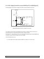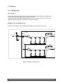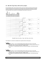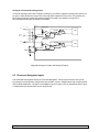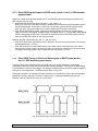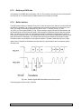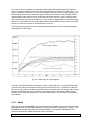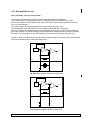
1
USER MANUAL
Hardware Part
SAA7709H/N1B
Car Radio Digital Signal Processor
Product Development CarDSP, Mainstream Consumer Systems Nijmegen, The Netherlands.
www.DataSheet.co.kr
Version nr. :
4.0
Author
:
G. Laarhoven
Status
:
Accepted
Date
:
January 8, 2002
Report nr.
:
RNB-C/3272/2002I-0005
Datasheet pdf - http://www.DataSheet4U.net/
REVISION HISTORY
Manual version
Date
Remarks
1.0
2.0
3.0
March 31, 2000
August 11, 2000
October 30, 2000
4.0
January 4, 2002
N101A initial version
N102B initial version
N103B initial version
• Radio features adapted
• RDS description adapted
N1B final version
• Fig. 8.15 : changed. Resistor R16/R18 is added
• Fig. 8.23 : changed. Resistor R5 is added
• Table 8.2 : Timing (unit) RDS changed
• Chapter 8.8 : Chapter “Interface with tuner
TEA6840 is added
www.DataSheet.co.kr
Philips Semiconductors Usermanual
2
SAA7709H/N1B
Datasheet pdf - http://www.DataSheet4U.net/
Summary.
The purpose of this manual is to give all hardware application information of theSAA7709H, being a Car
Radio Digital Signal Processor (CDSP), needed to make a hardware application. Also the audio and
radio features are described.
The audio and software part of the SAA7709H/N103B is decribed in a other document named “Software
Audio and Radio part SAA7709H/N103B”.
Before reading this report it is necessary to read first the data sheet of the SAA7709H.
In this manual all the pins are described with additional information on the input- and output circuits. The
blockdiagram is given and all functions are explained. All necessary coefficient settings and tables for
several selections are given. The application diagram is explained in detail.
www.DataSheet.co.kr
Philips Semiconductors Usermanual
3
SAA7709H/N1B
Datasheet pdf - http://www.DataSheet4U.net/
Table of Contents
1
INTRODUCTION.
7
2.
GENERAL DESCRIPTION.
8
3
HARDWARE/SOFTWARE FEATURES.
8
3.1
Hardware features
8
3.2
Software features
9
4
QUICK REFERENCE SPECIFICATION.
9
4.1
FM reception
9
4.2
AM reception
10
4.3
Analogue tape input
10
4.4
Analogue CD input
10
4.5
RDS reception
10
4.6
CD I2S / SPDIF input
4.7
Audio output performance
11
4.8
4.8.1
4.8.2
Audio processing
Volume/balance/fader/tone/loudness/dynamic bass boost control
Equalisation
11
11
11
5
11
www.DataSheet.co.kr
BLOCK DIAGRAMS.
12
5.1
Total block diagram
12
5.2
CDSP Block diagram.
13
6
6.1
7
PINNING DIAGRAM.
14
Pin description.
15
FUNCTIONAL DESCRIPTION OF THE CDSP MODES AND FUNCTIONS.
18
7.1
Audio processing
18
7.2
FM mode
19
7.4
General purpose tone generator
21
7.5
Tone sequencer
21
Philips Semiconductors Usermanual
4
SAA7709H/N1B
Datasheet pdf - http://www.DataSheet4U.net/
7.6
Noise generator
22
7.7
MSS function
22
7.8
Radio Data System (RDS) function
22
7.9
Second processor extension function
22
8
HARDWARE APPLICATION OF THE CDSP
23
8.1
Audio processing in DSP
8.1.1
Analogue outputs (pin 8, 9, 13 and 15)
8.1.2.
Internal reference voltage sources VREFDA (pin 12) and VREFAD (pin 77)
8.1.2.3
Ref. voltages for the AD convertors VDACP (pin 75) and VDACN (pin 76)
8.1.3
Power on/off mute
8.1.4
DSP Reset (pin 42)
23
23
24
25
26
28
8.2
30
AM / FM signal quality processing
8.3
FM mode
8.3.1
FM input pins
8.3.2
FM input sensitivity selection
8.3.3
FM IAC
31
31
32
34
8.4
AM, AUX, Tape, Phone, NAV and CD_A inputs
8.4.1 AM inputs
8.4.1.1
AM inputs for AM-mono mode and AM-stereo mode with external decoder
8.4.2 Tape / AUX input
8.4.3 Analogue CD input
40
42
42
44
45
8.5
47
Phone and Navigation inputs
www.DataSheet.co.kr
8.6
CD-digital inputs (I2S or SPDIF)
8.6.1 General
8.6.2 I2S input
8.6.3 SPDIF input
52
52
52
53
8.7
Radio Data System (RDS) function
8.7.1 General description
8.7.3 Direct RDS Inputs/outputs in DAVD mode (dac0=1, dac1=1, RDS decoder bypass mode)
8.7.4 Direct RDS Timing of Clock and Data signals in DAVD mode (dac0=1, dac1=1, RDS decoder
bypass mode)
8.7.5 Buffering of RDS data
8.7.6 Buffer interface
8.7.3 Fast RDS detection with the rds-band signal level detector
8.7.4 Bitslip
8.7.5 RDS/RBDS decoder
8.7.6 RDS/RBDS block detection
8.7.7 Error detection and correction
8.7.8 Synchronization
8.7.9 Flywheel for synchronization hold
8.7.10 Bit slip correction
8.7.11 Data processing control
8.7.12 Restart of synchronization mode:
8.7.13 Error correction control mode for synchronization:
8.7.14 RBDS processing mode:
8.7.15 Data available control modes:
8.7.16 Data output of RDS/RBDS information
53
53
56
Philips Semiconductors Usermanual
5
56
57
57
58
60
61
62
62
63
63
63
63
64
64
64
65
65
SAA7709H/N1B
Datasheet pdf - http://www.DataSheet4U.net/
8.8
Interface with Tuner TEA6840 (NICE)
66
8.9
I2C interface
68
8.10
Second processor extension function
69
8.11
Digital subwoofer and center output
69
8.12
External DAC output (subwoofer)
69
8.13
X-tal oscillator circuit
70
8.13
EMC SAA7709H application
72
8.14 Changing the clock frequency of the DSP
8.14.1 Procedure for increasing the clock frequency of the DSP
73
73
APPENDIX 1
74
:
APPLICATION DIAGRAM
www.DataSheet.co.kr
Philips Semiconductors Usermanual
6
SAA7709H/N1B
Datasheet pdf - http://www.DataSheet4U.net/
1
Introduction.
Digital techniques have been widely accepted in the audio world including in the Car Radio.
The CD was the first example, nowadays the digitisation of the Car Radio is a logical
continuation of this trend.
Furthermore, in the Car Radio world there is a growing demand not only for a good radio
perception but also for a better sound quality. People want the sound of their living room
in their vehicle. This led not only to the digitisation of analogue designs of the Car Radio, but also to the
incorporation of a customised DSP on board of a Car Radio I.C., delivering many possibilities for sound
quality improvement.
www.DataSheet.co.kr
Philips Semiconductors Usermanual
7
SAA7709H/N1B
Datasheet pdf - http://www.DataSheet4U.net/
2.
General description.
The CDSP-chip performs all the signal functions in front of the power amplifiers and behind the AM and
FM_MPX demodulation of a car radio or the tape input. These functions are: interference absorption,
stereo decoding, RDS demodulation and decoding, FM and AM weak signal processing (soft-mute,
sliding stereo, etc.), Dolby-B tape noise reduction and the audio controls (volume, balance, fader and
tone). Some functions have been implemented in hardware (stereo decoder, RDS decoding and IAC for
FM_MPX) and are not freely programmable. Digital audio signals from external sources with the Philips
2
I S and the LSB 16, 18, 20 and 24 bit justified format or SPDIF format up to Fs = 48 kHz are accepted.
There are four independent analogue output channels.
The SAA7709H/N103B is the final version. All audio and radio software features are in the N103
romcode available. The hardware of the IC between the N102B and N103B are the same.
The DSP contains a basic program which enables a set with AM/FM reception, compressor function for
all audio modes on the primary channel (channel 1) and fader/balance control. A hardware 5 band per
channel parametric equalizer is also implemented. With some restrictions also 2 different stereo
channels can be processed.
3
Hardware/software features.
3.1
Hardware features
•=1 Bit stream 1st order Sigma-Delta A/D converter with anti aliasing broadband input filter
•= 4 Bit stream 3rd order Sigma-Delta A/D converters with anti aliasing broadband input filter
•= 4 Bitstream D/A converters with 128-fold oversampling and noise shaping
•= 4 channel 5 band I C controlled parametric equalizer
2
www.DataSheet.co.kr
•= Integrated semi-digital filter, no external post filter required for D/A.
•= A stereo I S output with 256 Fs clock for connection to an external DA converter.
2
•= Limited dual media support, allowing limited separate front-seat and rear-seat signal sources and
separate control.
•= Digital FM stereo decoder.
•= Digital FM interference Suppression.
•= RDS demodulation decoding via separate ADC, with buffered output option on the demodulator and
2
decoder I C accessible.
•= Two mono CMRR or differential input high performance stages for voice signals from Phone and
Navigation inputs via 3rd order Sigma-Delta A/D converter.
•= Four switchable stereo CMRR or differential input stages. (CD-walkman, CD-changer etc.)
•= Analogue single ended tape input
•= A 5120 X 32 DSP Program ROM, a 1024 X 24 Data Ram and a 640 X 12 Coefficient RAM.
•= Separate AM-left and AM-right inputs in case of use of external AM stereo decoder.
•= One digital input: I S or LSB justified format.
2
•= Two digital inputs: SPDIF format at Fs = 48 kHz maximum.
•= Audio output short circuit protected
•= I C bus controlled (including fast mode)
2
Philips Semiconductors Usermanual
8
SAA7709H/N1B
Datasheet pdf - http://www.DataSheet4U.net/
•= A Phase Lock Loop derives the internal clock for the DSP from one common fundamental crystal
oscillator
•= A Phase Lock Loop derives the internal clock for the DAC and other parts of the IC from a digital input
Word Select
•= Combined AM/FM level input
•= Relative high pin compatibility with SAA7704, SAA7705, SAA7706, SAA7708 (incidental minor
replacements needed)
•= Low number of external components required
•= -40 to +85 C operating temperature range
o
•= Easy applicable
3.2 Software features
•= FM de-matrixing
•= AM brick wall filter
•= Baseband Audio processing (balance/fader/volume)
•= Soft Audio Mute
•= Large volume jumps e-power interpolated for smooth volume steps
•= General Purpose Tone Generator
4
Quick reference specification.
Important: This overview shows the best specification which can be obtained with an 'ideal' receiver
in combination with the SAA7709H. However the specification points 4.1 and 4.2 will be limited by
the front-end receiver and not by the SAA7709H.
www.DataSheet.co.kr
4.1
FM reception
Frequency response(+/-1 dB)
20 Hz - 17 kHz
S/N (mono, 1KHz, 22.5 kHz dev.)
(deemphasis 50 µs)
> 69 dB ; typical 72 dB
S/N (stereo, 1 kHz, 22.5 kHz dev.)
(deemphasis 50 µs)
> 60 dB ; typical 63 dB
Max. deviation (at THD < 1%) at 1 kHz
> 120 kHz
Mono distortion, 1 kHz
at 75 kHz deviation
at 22.5 kHz deviation
< 0.2 %
< 0.1 %
Stereo distortion, 1KHz, 1 channel
at 22.5 kHz deviation
< 0.2 %
Stereo channel separation, 1 kHz
> 40 dB ; typical 45 dB
Philips Semiconductors Usermanual
9
SAA7709H/N1B
Datasheet pdf - http://www.DataSheet4U.net/
4.2
4.3
AM reception
Frequency response with tuner
20 Hz - 2 kHz
Frequency response (+/-1 dB) with DSP software brickwall
filter (without tuner)
Frequency response (+/-1 dB) without brickwall filter
(without tuner)
S/N at 1 kHz, 30 % AM
20 Hz - 4.5 kHz
> 70 dB ; typical 75 dB
Distortion, 400 Hz, BW 5 kHz
80 % AM
30 % AM
< 0.2 %
< 0.1 %
20 Hz - 15 kHz
Analogue tape input
Frequency response (+/-3 dB)
20 Hz - 18 kHz
Typ. S/N at 1 kHz, 0 ref. dB
84 dB
Typ. THD+N, 1 kHz (0.55 Vrms)
-85 dB
Typ. channel separation, 1 kHz
65 dB
RDS traffic information reception from radio signals in this mode is possible; the decoder is
still operating
www.DataSheet.co.kr
4.4
Analogue CD input
Frequency response (+/-3 dB)
20 Hz - 18 kHz
Typ. S/N at 1 kHz, 0 dB ref.
84 dB
Typ. THD+N, 1 kHz (0.5 Vrms)
-85 dB
Typ. channel separation, 1 kHz
65 dB
RDS traffic information reception from radio signals in this mode is possible; the decoder is
still operating
4.5
RDS reception
Min. nearby selectivity
(neighbour ch at 200 kHz)
61 dB
Min. pilot attenuation
50 dB
Philips Semiconductors Usermanual
10
SAA7709H/N1B
Datasheet pdf - http://www.DataSheet4U.net/
4.6
CD I2S / SPDIF input
The performance of these input signals is actually limited by the DAC output, as described in
chapter 4.7.
The digital CD input can be used as an alternative input for the analogue CD.
RDS traffic information reception from radio signals in this mode is possible; the decoder is
still operating
4.7
4.8
Audio output performance
Typ. output level
1 Vrms
Bandwidth (fs=44.1 kHz, -3dB)
20 Hz - 22 kHz
Typ. S/N
105 dBA
Typ. output noise
3 µV ; A-weighted
Typ. THD+N, 1 kHz, 0 dB
-90 dB
Typ. Dynamic Range, 1 kHz (-60 dB)
97 dBA
Audio processing
www.DataSheet.co.kr
4.8.1
Volume/balance/fader/tone/loudness/dynamic bass boost control
(figures count for default coefficient set)
4.8.2
Volume control range
-66 dB --> +24 dB
Balance attenuation range (Left/Right)
0 dB --> -66 dB
Fader attenuation range (Front/Rear)
0 dB --> -66 dB
Equalisation
Number of bands
20 bands
Filter order
2nd order BP
Centre frequency
20 Hz --> 18 kHz
Gain control range
-30 dB --> +12 dB
Quality factor
0.01 --> 100
Philips Semiconductors Usermanual
11
SAA7709H/N1B
Datasheet pdf - http://www.DataSheet4U.net/
5
5.1
Block diagrams.
Total block diagram
PHONE/NAV
TAPE
CD_A
AUX
SPDIF-2
SPDIF-1
CD_D
The total block diagram indicates a possible application in which the CDSP can be used.
AM/FM-RF
TEA6811
AM
FM
AM/FM-IF
RDS
TEA6824 Level
audio
co-processor
LR
SAA7709H
RR
LF
RF
POWER
AMP
I2C
I2S
External DAC
I2C
µP
RDS
Display
www.DataSheet.co.kr
Fig 5.1 Total block diagram
Philips Semiconductors Usermanual
12
SAA7709H/N1B
Datasheet pdf - http://www.DataSheet4U.net/
CDSP Block diagram.
DSP_IO(1..8)
5.2
SAA7709H
PHONE
FRONT-LEFT
PHONE_GND
DIGITAL SOURCE SELECTOR
NAV
STEREO ADC1
NAV_GND
CD_R
CR_GNDR
CD_L
ANALOG
CD_GNDL
SOURCE
TAPE_R
TAPE_L
SELECTOR
STEREO ADC2
DSP
FSDAC
REAR-LEFT
REAR-RIGHT
FS_SYS
I2S OUT
AM_R
FRONT-RIGHT
QUAD
AM_L
AUX_R
CLK_DAC
WS_DAC
DATA_DAC
AUX_L
FM_MPX
FM_RDS
Digital I/O
IIS_OUT1
SEL_FR
IIS_OUT2
IIS_CLK
IIS_WS
IIS_IN1
IIS_IN2
LEVEL
XTAL
RDS
LEVEL ADC
I2S
I2C
SPDIF
osc
demodulator
AO
SDA
SCL
OSC_OUT
OSC_IN
RDS_CLOCK
RDS_DATA
SPDIF2
SPDIF1
CD_CLK
CD_DATA
CD_WS
www.DataSheet.co.kr
Fig 5.2 Block diagram CDSP
Philips Semiconductors Usermanual
13
SAA7709H/N1B
Datasheet pdf - http://www.DataSheet4U.net/
25
26
SPDIF1
DSP_IO5
CD_WS
CD_DATA
27
CD_CLK
29
28
IIS_CLK
IIS_IN1
31
30
IIS_WS
IIS_IN2
32
33
34
IIS_OUT1
IIS_OUT2
VDDQ2
35
VSSQ2
37
36
DSP_IO2
38
39
40
DSP_IO1
Pinning diagram.
DSP_IO3
6
41
24
42
23
S P D IF 2
D S P _ IO 4
VSSQ1
DSP_RESET
43
22
44
21
45
20
VDDQ1
RTCB
D S P _ IO 6
SH TC B
C LK _D AC
TSCAN
46
19
47
18
48
17
D ATA_DA C
VDDQ3
W S_DAC
SAA7709H
VSSQ3
VDDD1
49
VSSS1
50
VSSS2
51
VDDD2
52
VSSS3
53
VSSS4
54
VSSS5
55
VSSS6
56
AO
57
FS_S YS
16
D S P _ IO 7
15
FLV
14
D S P _ IO 8
13
FRV
12
VR E FD A
11
VDDDA
10
VSSDA
9
R LV
8
RRV
SCL
7
58
PO M
SDA
6
59
N RV_G N D
R D S_C LO C K
5
60
www.DataSheet.co.kr
R DS_DATA
NAV
61
4
62
3
63
2
PH O N E _G N D
SE L_FR
PHO NE
VS S_O SC
LEVEL
O S C _ IN
1
64
O SC_OU T
FM_RDS
AUX_L
80
79
AUX_R
78
VREFAD
VDACN
77
76
VDACP
75
74
VDDAAD
CD_GNDL
73
CD_L
CD_GNDR
72
71
CD_R
70
TAPE_L
69
TAPE_R
68
AM_L
67
AM_R/AM_MONO
VDD_OSC
66
65
FM _M P X
Fig 6.1 Pinning diagram
Philips Semiconductors Usermanual
14
SAA7709H/N1B
Datasheet pdf - http://www.DataSheet4U.net/
6.1 Pin description.
Table 1 Pin list SAA7709H
SYMBOL
PIN
DESCRIPTION
FM_MPX
1 Analogue input pin for FM-Multiplex signal
LEVEL
2 FM/AM-level input pin. Via this pin the level of the FM signal or level of the AM signal is fed to the
CDSP. The level information is used in the DSP for signal correction
PHONE
3 Input of common mode phone signal
PHONE_GND
4 By I2C switchable common mode reference pin to enable an arbitrary high common mode analogue input
for all 4 ADs.
NAV
5 Input of common mode navigation signal
NAV_GND
6 By I2C switchable common mode reference pin to enable an arbitrary high common mode analogue input
for all 4 ADs.
POM
7 Power on Mute of the FSDAC. Timing is determined by an external capacitor and the internal current
sources.
RRV
8 Rear Right audio voltage output of the FSDAC
RLV
9 Rear Left audio voltage output of the FSDAC
VSSDA
10 Ground supply analogue part of the FSDAC and SPDIF bitslicer
VDDDA
11 3V3 positive supply analogue part of the FSDAC and SPDIF bitslicer
VREFDA
12 Voltage reference of the analogue part of the FSDAC
www.DataSheet.co.kr
FRV
13 Front Right audio voltage output of the FSDAC
DSP_IO8
14 Digital in/output 8 of the DSP-core (F7 of the status register)
FLV
15 Front Left audio voltage output of the FSDAC
DSP_IO7
16 Digital in/output 7 of the DSP-core (F6 of the status register)
FS_SYS
17 256- or N X FS clock output to be used together with an external DA converter
WS_DAC
18 Word Select signal to be used for an external DA converter
DATA_DAC
19 Data signal to be used for an external DA converter
CLK_DAC
20 Clock signal to be used for an external DA converter
DSP_IO6
21 Digital in/output 6 of the DSP-core (F5 of the status register)
VDDQ1
22 3V3 positive supply 1 peripheral cells only
VSSQ1
23 Ground supply 1 of peripheral cells only
SPDIF2
24 Analogue bitslicer input2 for SPDIF, can be selected i.s.o. SPDIF1 via I2C bit
SPDIF1
25 Analogue bitslicer input1 for SPDIF, can be selected i.s.o. SPDIF2 via I2C bit
Philips Semiconductors Usermanual
15
SAA7709H/N1B
Datasheet pdf - http://www.DataSheet4U.net/
DSP_IO5
26 Digital in/output 5 of the DSP-core (F4 of the status register)
CD_WS
27 I2S or LSB justified format Word select input from a digital audio source
CD_DATA
28 I2S or LSB justified format Left-Right Data input from a digital audio source
CD_CL
29 I2S Clock or LSB justified format input from a digital audio source
IIS_CLK
30 Clock output for external I2S receiver. For example headphone/ subwoofer
IIS_IN1
31 Data 1 input for external I2S transmitter, e.g. audio co-processor
IIS_IN2
32 Data 2 input for external I2S transmitter, e.g. audio co-processor
IIS_WS
33 Word select output for external I2S receiver. For example headphone/ subwoofer
IIS_OUT1
34 Data1 in/output for external I2S receiver. For example headphone/ subwoofer
IIS_OUT2
35 Data2 in/output for external I2S receiver. For example headphone/ subwoofer
VDDQ2
36 3.3 V positive supply 2 peripheral cells only
VSSQ2
37 Ground supply 2 of peripheral cells only
DSP_IO1
38 Digital in/output 1 of the DSP-core (F0 of the status register). Input level must always be defined
externally in the application
DSP_IO2
39 Digital in/output 2 of the DSP-core (F1 of the status register). Input level must always be defined
externally in the application
DSP_IO3
40 Digital in/output 3 of the DSP-core (F2 of the status register)
DSP_IO4
41 Digital in/output 4 of the DSP-core (F3 of the status register)
DSP_RESET
42 Reset of the DSP core (active low)
RTCB
43 Asynchronous Reset Test Control Block active low, may not be connected in the application
SHTCB
44 Shift Clock Test Control Block, may not be connected in the application
TSCAN
45 Scan control active high, may not be connected in the application
VDDQ3
46 3V3 positive supply 3 peripheral cells only
VSSQ3
47 Ground supply 3 peripheral cells only
VDDD1
48 3V3 positive supply 1 core and internal supply IO ring
VSSS1
49 Ground supply 1 of 3.3 volt core only
VSSS2
50 Ground supply 2 of 3.3 volt core only
VDDD2
51 3V3 positive supply 2 core only
VSSS3
52 Ground supply 3 of core, internal ground supply ring and substrate
VSSS4
53 Ground supply 4 of core, internal ground supply ring and substrate
VSSS5
54 Ground supply 5 of core only
Philips Semiconductors Usermanual
www.DataSheet.co.kr
16
SAA7709H/N1B
Datasheet pdf - http://www.DataSheet4U.net/
VSSS6
55 Ground supply 6 of core only
A0
56 Slave sub-address I2C selection / Serial data input test control block
SCL
57 Serial clock input I2C bus. Must always be defined by application.
SDA
58 Serial data input / output I2C bus
RDS_CLOCK
59 Radio Data System bit clock output / RDS external clock input
RDS_DATA
60 Radio Data System data output
SEL_FR
61 AD input selection switch to enable high ohmic FM_MPX input at fast tuner search on FM_RDS input.
Must always be defined by application.
VSS_OSC
62 Ground supply crystal oscillator circuit
OSC_IN
63 Crystal oscillator input: crystal oscillator sense for gain control or forced input in slave mode
OSC_OUT
64 Crystal oscillator output: Drive output to 11.2896 MHz crystal
VDD_OSC
65 3V positive supply crystal oscillator circuit
AM_R/AM_MONO
66 Analogue input pin for AM audio frequency Right Channel
AM_L
67 Analogue input pin for AM audio frequency Left Channel or AM mono
TAPE_R
68 Input of the analogue TAPE Right signal
TAPE_L
69 Input of the analogue TAPE Left signal
CD_R
70 Input of the analogue CD Right signal
CD_GNDR
71 By I2C switchable common mode reference pin to enable high common mode analogue input for the
CD_R input or a high common mode analogue input for all 2 ADs for right channel processing
www.DataSheet.co.kr
CD_L
72 Input of the analogue CD Left signal
CD_GNDL
73 By I2C switchable common mode reference pin to enable high common mode analogue input for the
CD_L input or a high common mode analogue input for all 2 ADs for left channel processing
VDDAAD
74 Positive supply analogue AD1..4 and Level AD.
VDACP
75 Positive reference voltage ADC1..4 and Level AD
VDACN
76 Ground supply analogue AD1..4 and Level AD.
VREFAD
77 Common mode reference voltage AD1..4 and Level AD
AUX_R
78 Input of the analogue Auxiliary Right signal
AUX_L
79 Input of the analogue Auxiliary Left signal
FM_RDS
80 Analogue input pin for FM RDS signal
Philips Semiconductors Usermanual
17
SAA7709H/N1B
Datasheet pdf - http://www.DataSheet4U.net/
7
Functional description of the CDSP modes and functions.
Introduction.
The CDSP block diagram is depicted in figure 5.1. For a thorough description of the CDSP block
diagram see the data sheet of the SAA7709H. In this chapter a general overview is given of all
modes and functions.
The CDSP can be set in several operation modes. Each mode executes functions which are required
for that particular mode, furthermore the CDSP can process two independent sources simultaneously
(dual media modes), note that NOT all combinations are possible, for example AM-mode and FM-mode,
two digital input modes are only possible when the the (external) digital sources are synchronous and
locked to each other.
The selection of a particular mode is software controlled (via the I2C bus) and described in chapter 9.
The required inputs for each mode can be selected by the analogue or digital source selectors which
are software controlled (via the I2C bus). The source selection is also described in chapter 9.
7.1 Audio processing
All basic audio processing in the CDSP chip is performed by the integrated digital signal processor
(DSP).
The signal flow is more or less fixed and the functions are controlled by sending coefficient values to the
appropriate places in the DSP processor coefficient memory via the I²C bus.
The functions of the Audio processing block are always executed independent of the mode.
The Audio processing block consists of two parts, the audio processing functions for the primary
channel and the audio processing functions for the secondary channel.
www.DataSheet.co.kr
The following functions have been implemented:
- Volume control
The volume control function determines the output voltage of the CDSP. The volume control is split into
a gain and a attenuation section which acts equal for both channels. The volume control contains also a
prescaling which ensures that for the various input signals the same sound pressure level (for a
fixed volume setting) can be obtained at the output of the CDSP. The primary- and secondary channel
have independent volume control.
- Balance
The balance function controls the attenuation of either the left or the right channel while the other
channel is kept constant. Separate balance functions are available in the primary- and secondary
channel.
- Fader
This function is only implemented for the primary channel
The fader function controls the attenuation of either the front or rear channels while the other channels
are kept constant. The fader is controlled via the I2C bus.
- Soft audio mute
The soft audio mute function enables the user to generate a gradual mute or de-mute function without
Philips Semiconductors Usermanual
18
SAA7709H/N1B
Datasheet pdf - http://www.DataSheet4U.net/
undesired clicks. The Soft Audio Mute is implemented as a linear ramp. There is one SAM function for
the primary channel and the subwoofer output, the secondary channel has a separate SAM function.
- Parametric Equaliser
2 sections of 2x5 bands each are available, they can be used in the primary and/or the secondary
channel in the main audio program.
7.2 FM mode
This is the mode for FM reception and runs in the DSP. The selected input is FM-MPX or FM-RDS
The program in the FM mode offers the following functions:
Enhanced FM dynamic signal processing
The FM dynamic signal processing adapts the FM audio characteristics depending on the quality of the
received station. As criterium to judge this quality the following parameters are used:
-
the level signal as a measure for the fieldstrength
the multipath detector output as a measure for the multipath distortion
the noise above 60 kHz of the MPX signal as a measure for the adjacent channel
interference
From the audio characteristics the output level (softmute), the stereo image (sliding stereo to
mono) and the audio frequency response (high cut control) are adapted. The following functions
are implemented:
• Softmute as a funtion of level and noise:
- fast attack and recovery at level dips with a low repetition rate
- fast attack with slow recovery at dips with a high repetition rate or with a long duration
- fast attack and recovery at adjacent channel breakthrough
www.DataSheet.co.kr
• Stereo control (sliding stereo) as a function of level, noise and multipath:
- fast attack and recovery at level dips, noise or multipath bursts with a low repetition rate
- fast attack with slow recovery at events with a high repetition rate or with a long duration
• Audio frequency response control as a function of level, noise and multipath:
- fast attack and recovery at level dips, noise or multipath bursts with a low repetition rate
- fast attack with slow recovery at events with a high repetition rate or with a long duration.
Adjustment of channel separation
The purpose of this function is to compensate for the non flat frequency response around 38 kHz of
the FM tuner which causes extra cross-talk.
FM De-emphasis filter and 19 kHz MPX filter
The purpose of the de-emphasis filter is to compensate the pre-emphasized FM signal with a filter with
a time constant of 50 µs or 75 µs. The notch filter at 19 kHz is used to protect tweeters in high power
applications from overload by the stereo pilot.
FM audio filter
The purpose of the FM audio filter is to set the audio bandwidth in FM mode independent from the
Philips Semiconductors Usermanual
19
SAA7709H/N1B
Datasheet pdf - http://www.DataSheet4U.net/
other modes.
Stereo detection
The purpose of the stereo detector is to indicate the presence of a pilot tone and that the stereo
decoder is in lock.
Noise filter
The noise level is detected in a band from 60 kHz till 120 kHz with an envelope detector (see data
sheet). The noise level is used as adjacent channel information for the controller and for the FM
dynamic signal processing.
RDS updates
This function offers the following features:
- Pause detection
The purpose of the pause detection is to search for a pause in the FM signal.
A pause is detected when the FM signal is below a pre-defined level for a certain amount of time.
The output of the pause detector is the DSP_IO4 pin (pin 41). "High" indicates pause.
-
Mute
The purpose of the mute is to mute the FM signal that goes to the audio processing block.
This mute is activated by the external control pin DSP_IO1 (pin 38). "Low" is mute.
-
Hold function
The purpose of the hold function is to prevent that the information retrieved during an RDS update
can disturb the filters in the FM signal processing block. The hold function is activated by the
external control pin DSP_IO1 (pin 38). "Low" is hold.
-
Freeze function
The purpose of the freeze function is to freeze the level, noise and multipath values measured
during an RDS update and to read them out after the update. The freeze function is activated by
the external control pin DSP_IO2 (pin 39). "Low" is freeze.
www.DataSheet.co.kr
Interference absorption circuit (IAC)
The Interference Absorption Circuit (IAC) detects and suppresses ignition interference.
The characteristics of the IAC can be adapted to the properties of different FM tuners by means of the
predefined coefficients in the IAC control register. The values can be changed via the I²C bus.
On power on the nominal setting for a good performing IAC is selected (all IAC control bits are set to
their default value, according the I2C hardware register definition).
Philips Semiconductors Usermanual
20
SAA7709H/N1B
Datasheet pdf - http://www.DataSheet4U.net/
7.3
AM-mono mode
This is the mode for mono MW, LW or SW reception, the selected input is AM_R.
The program in the AM-mono mode runs in the DSP and offers the following functions:
AM dynamic signal processing
The AM dynamic signal processing adapts the AM audio characteristics depending on the
quality of the received station. As criterium to judge this quality the level signal as a measure
for the fieldstrength is used.
From the audio characteristics the output level (softmute) and the audio frequency response
(high cut control) are adapted. The following functions are implemented:
• Soft mute as a function of level
• Audio frequency response control as a function of level
6th order Low-pass filter
The purpose of the low-pass filter is to suppress interference whistles from adjacent channels
and noise.
AM IAC
The AM IAC (interference absorption circuitry) detects and eliminates audible clicks caused by
impulsive interference, such as caused by engine ignition or fan, on AM reception.
The characteristics of the AM IAC can be adapted to the properties of different AM tuners by means of
coefficients in the YRAM of the DSP
AM Quality detection
www.DataSheet.co.kr
The AM Quality feature detects interfering signals caused by adjacent- and co-channel interference.
This feature is available only during search mode of the AM-tuner. The audio output is muted during
search mode.
7.4 General purpose tone generator
The tone generator generates a sinewave signals on the Left- and Right audio channel and can be
selected as main audio source. The tone generator can be used f.i. to test the speaker outputs in the
car radio during production. The tone generator function is part of the audio program in the DSP and is
therefor always available.
7.5 Tone sequencer
The tone sequencer generates a wide range of bleeps and chime sounds with selectable frequency and
wave form. These sounds can be used for audio feedback or for test purposes and can be added to the
Primary and/or Secundary channel outputs.
The tone sequencer function is part of the audio program in the DSP and is therefor always available.
Philips Semiconductors Usermanual
21
SAA7709H/N1B
Datasheet pdf - http://www.DataSheet4U.net/
7.6 Noise generator
The noise generator produces white noise, the purpose of this function is automatic car aucoustic
measurements. The noise generator has an optional octave-band filter.
7.7 MSS function
The purpose of the Music Search (MSS) function is to search for the next pause on a cassette tape.
The output of the MSS mode is the DSP_IO5 pin (pin 26). This pin is "High" when the level of the input
signals remain below a pre-defined level for a certain amount of time.
7.8 Radio Data System (RDS) function
The selected input for this function is either FM-RDS or FM-MPX.
This function offers the following features:
-
-
Demodulation of the inaudible RDS information, which is transmitted by FM broadcasting and is sent
it to a suitable external decoder. Also a internal RDS decoder is available to decode the
demodulated RDS information. RDS information is then available via I2C communication.
two tuners concept. There are two different input pins from which the RDS information can be
retrieved. The demodulated RDS information is available by each bit or buffered by 16 bits.
www.DataSheet.co.kr
7.9 Second processor extension function
This function offers the possibility of the addition of a second DSP which offers special, more
sophisticated features such as acoustic and room effects.
Philips Semiconductors Usermanual
22
SAA7709H/N1B
Datasheet pdf - http://www.DataSheet4U.net/
8
Hardware application of the CDSP
General
In this chapter the external components are discussed, sometimes in combination with the on
chip input/output circuits.
How to select specific inputs and operating modes is described in chapter 9 of this manual.
The external components are depicted in the CDSP application diagram which can be found in
appendix 1. It must be stressed here that this application diagram is an example, not the ultimate
application diagram.
There is also an application diagram of the application board (not in the usermanual) and that contains
much more components in order to optimise the EMC.
8.1 Audio processing in DSP
In this chapter the following hardware functions will be covered
-
Analogue outputs (D/A convertors)
Voltage and current reference sources
Power on/off mute
DSP reset
8.1.1 Analogue outputs (pin 8, 9, 13 and 15)
There are 4 analogue outputs namely those which make the outputs of the 4 bitstream DACs (Front
Left/Right and Rear Left/Right). The D/A convertors contain an internal filter so no external filter is
required. The basic block diagram of one analogue output is depicted in figure 8.1.
www.DataSheet.co.kr
Rint
1 µF
-
+
100 Ohm
Analog out
+
10 kOhm
10 nF
Vref
IDAC
CDSP
Fig. 8.1 Analogue output block diagram
Philips Semiconductors Usermanual
23
SAA7709H/N1B
Datasheet pdf - http://www.DataSheet4U.net/
An analogue output consists mainly of a current to voltage convertor.
A current to voltage convertor is constructed by using the internal CMOS op-amp and resistor as
depicted in figure 8.1. The current from the Bistream DAC is converted into a voltage via Rint.
The full scale output voltage of the DAC is 1 Vrms. The DAC outputs require a AC load that may not
drop under the 2 kΩ. In the application 10 kΩ resistors are used (R26, R28, R30 and R32).
The DC output voltage is the same as VREFDA (typ. 1.65V). This DC is removed by the electrolytic
capacitors C34, C36, C38 and C40. The cut-off frequency (and phase non-linearity) of these high pass
filters depends on the DAC load resistance and/or input impedance of the equipment behind the CDSP.
The extra 1st order RC filter is to suppress radiation from the analogue output to the outside world
(fc = 160 kHz) (R27, R29, R31, R33, C35, C37, C39, C41). The cut-off frequency is not critical
(component tolerance of 20% is tolerable). These filters may be omitted if considered not necessary.
8.1.2. Internal reference voltage sources VREFDA (pin 12) and VREFAD (pin 77)
The block diagram of the reference voltage sources VREFDA and VREFAD is depicted in figure 8.2.
100 k
VDDA2
10k
DC-bias
analog inputs
100 k
Ω
Int. VREF
for DAC
BUFFER
VREFDA
100 k
+
www.DataSheet.co.kr
CREFDA
10k
BUFFER
VREFAD
(C42)
C11
47 nF
Ω
+
C12
22 µF
CDSP
Fig. 8.2 Internal reference voltage sources block diagram
The supply voltage VDDA2 is divided by two internal 10 kΩ resisters and buffered. The output of the first
buffer is called the internal Vref and is used as the reference voltage for the D/A convertors.
The output of the second buffer is connected to pin VREFAD (pin 77) and is internally used as the 1.65
V reference voltage of the switch capacitor D/A convertors (and buffers) of the
level A/D convertor, ADC1/2 and ADC3/4.
As filtering for the internal reference voltages a capacitor is added at the VREFDA pin.
In the CDSP application we use:
f >= 1 kHz (Vripple=100 mV), ripple rejection (PSRR)= typ. 60 dB, CREFDA=22 µF (C42).
The VREFAD voltage is also used as a DC-bias for the analogue AM, Tape and CD inputs via
82 kΩ / 100 kΩ resistors. Due to the low output impedance of the buffer, the crosstalk between the
analogue inputs is ≤ -74 dB at DC, the external 22 µF elco (C12) is added to further improve the
crosstalk rejection to ≤ -80 dB at 1 kHz. The 47 nF capacitor (C11) is added to remove high frequency
noise on the midref voltage for the A/D convertors.
Philips Semiconductors Usermanual
24
SAA7709H/N1B
Datasheet pdf - http://www.DataSheet4U.net/
8.1.2.3 Ref. voltages for the AD convertors VDACP (pin 75) and VDACN (pin 76)
The block diagram of the reference voltages for the AD convertors is depicted in figure 8.3.
VDDAAD
R34
10
Ω
VDACP
C43
100 µF
reference voltage
ADC
+
Ri = 40 k
VDACN
reference voltage
ADC
Fig. 8.3 Block diagram reference voltages AD convertors.
www.DataSheet.co.kr
The voltages at the pins VDACP and VDACN1 are the reference voltages for the AD convertors, for
good performing AD’s it is important that these reference voltages are clean.
The external 10 Ω resistor (R34) and 100 µF elco (C43) filter the analogue supply voltage VDDAAD and
are added to improve the power supply rejection ratio (PSRR).
In the CDSP application we use:
f >= 1 kHz (Vripple=100 mV), ripple rejection (PSRR)= typ. 39 dB, CREFDA=100µF (C43).
Philips Semiconductors Usermanual
25
SAA7709H/N1B
Datasheet pdf - http://www.DataSheet4U.net/
8.1.3 Power on/off mute
The block diagram of the power on mute (POM) circuit is depicted in figure 8.4.
COMPARATOR
< 500 mV
16µA
96µA
S
I POM
POM
CPOM
(C32)
+
22µF
Fig. 8.4 Power on mute block diagram
Power on Mute (pin 7)
www.DataSheet.co.kr
To avoid any uncontrolled noise at the audio outputs after power-on/off of the IC, the internal
reference current source of the D/A converter is controlled. The capacitor on the POM pin (C32)
determines the switch-on timing of this current. See figure 8.5
At power-on the the switch S is closed and the current out of the POM pin (IPOM) is 16 µA, the capacitor
Cpom gets charged by IPOM and the voltage at the POM pin (VPOM) increases linearly until VPOM = 0.5 V,
at this point the comparator is triggered and switch S is opened. As a result IPOM becomes 112 µA and
VPOM increases fast until it reaches VDDA.
As a result of this POM control the Vout-AC at the DAC outputs (in dB) increases almost dB linear
from -100 dBFS till 0 dBFS.
At time=tpom the DAC output Vout-AC = -25 dBFS, before this output voltage is reached the chip must
be resetted. After the reset the chip comes automatically in the idle mode via the DSP program (see
also chapter 9). This DSP program sets the outputs of the digital upsampling filters to digital silence
and therefore the AC output current of the DAC's to 0 µA (see also in the next chapter).
The time tpom as function of Cpom is :
tpom = 0.03125 * Cpom
( Cpom in µF)
The time ts during which the output voltage further increases from -25 dBFS to 0 dBFS is :
ts = 0.8 * tpom
In the CDSP application we use:
Tpom = 690 msec (± 20%)
Cpom = 22 µF (C32)
Philips Semiconductors Usermanual
26
SAA7709H/N1B
Datasheet pdf - http://www.DataSheet4U.net/
VPOM [V]
VDDA
0.5
tpom
DAC
VOUT - AC
time [sec]
0
[dBFS]
www.DataSheet.co.kr
-25
-100
tpom
time [sec]
Fig. 8.5 Switch-on timing DAC
Philips Semiconductors Usermanual
27
SAA7709H/N1B
Datasheet pdf - http://www.DataSheet4U.net/
Power off plop suppression
To avoid plops in a power amplifier, the supply voltage of the analogue part of the D/A converter and the
op-amps are fed by an external voltage regulation circuit (R9, R10 and TR2) and an extra capacitor
(C31) as indicated in the application diagram. During power-off the output voltage will decrease
gradually, allowing the power amplifier some extra time to switch off without audible plops.
In addition the POM should be pulled to zero by the µProcessor before the power supply of the digital
circuitry (VDDDD1, VDDDD2) is below 2.2V. Below this value the digital
circuitry is undefined and can therefore cause extra undesirable clicks during power-off.
8.1.4 DSP Reset (pin 42)
The reset pin is active low and requires an external pull-up resistor of 47 kΩ. Between the reset pin and
the ground a capacitor should be connected to allow a proper switch-on of the supply voltage. The
capacitor value is such that the chip is in reset as long as the power supply is not stabilised. A more or
less fixed relationship between the DSP reset (pin 42) time constant and the POM (pin 7) time is
obligatory. The voltage on the POM pin determines the current flowing in the DACs. At 0 V at the POM
pin the DAC currents are zero and so are the DAC output voltages. At 3.3 V the DAC currents are at
their nominal value. Long before the DAC outputs get to their nominal output voltages, the DSP must be
in working mode to reset the output register of the digital filter, therefore the DSP reset time constant
must be shorter than the POM time (tpom).
The dsp reset input is a digital input (with hysteresis) and that means that the dsp reset circuit is
enabled when Vcdspres=80%Vdd.
In the CDSP application we use:
Tdspres
Cdspres
= 68 - 92 msec (tolerance is due to tolerance of the external pull-up resistor
and the capacitor tolerance (10%)
= 1 µF)
www.DataSheet.co.kr
In calculating Tdspres it is assumed that Vcdspres=80%Vddd and the formula to calculate Tdspres is:
Vcdspres = Vddd ∗ (1 − e − Tdspres / RC )
The reset has the following functions:
-
the bits of the I2C hardware register are set to their preset values
the program counter is set to address $0000
DSP_IO1 .. DSP_IO7
When the level on the reset pin is at logical high (Vcdspres=80%Vddd), the DSP program in the DSP
starts to run from the idle mode, resets the output registers of the digital filters and the µProcessor can
start sending commands.
General timing requirements are:
Tdspres
Tpom
TµPcomm
>
>
>
Tpower
Tdspres
Tdspres
Figure 8.6 gives an overview of the several time constants.
Philips Semiconductors Usermanual
28
SAA7709H/N1B
Datasheet pdf - http://www.DataSheet4U.net/
VDDD
Vpom
0.7 V
Tpom = 690 msec
Vdspres
80%
Tdspres= 68 - 92 msec
µPcomm
> 150 msec
www.DataSheet.co.kr
.
Fig. 8.6 Power-up timing diagram to avoid clicks
Philips Semiconductors Usermanual
29
SAA7709H/N1B
Datasheet pdf - http://www.DataSheet4U.net/
8.2 AM / FM signal quality processing
Level (pin 2)
The basic circuit diagram of the level input is depicted in figure 8.7.
CDSP
R4
Level
Ri > 1.5 MΩ
R5
C4
Fig. 8.7 Level input
The level signal from the tuner is divided with resistors R4 and R5 in order to match the conversion
range of the Level A/D convertor to the tuner properties.
With R4, R5 and C4 a first order low pass filter is realised at the level input.
The cut-off frequency of this filter is :
www.DataSheet.co.kr
1
fc =
R 4 ⋅ R5
2 ⋅π ⋅
⋅ C4
R 4 + R5
The low pass filter at the input of the FM level pin has two functions:
•
to avoid aliasing in the level A/D convertor, that means that frequency components of
f > 1/2 fsA/D < 54 dB below the maximum input of the level A/D convertor (figure for S/N for level
A/D convertor, mentioned in data sheet)
•
to create a filter for the multipath detector with a cut-off frequency of 34 kHz (± 20%)
These functions are realised with R4=27 kΩ (± 10%), R3=100 kΩ (± 10%) and C1= 220 pF (± 10%).
The capacitor is connected to the ground plane.
Remarks:
a) The source resistance is not taken into account because this Rsource << (127 kΩ ) otherwise the
cut-off frequency is affected.
b) The input resistance of the CDSP is not taken into account because this Rin is big (1.5 MΩ min.).
The conversion range of the A/D convertor is from 0 V to VDDA1 (see spec in the data sheet).
The voltage range of the FM level information has to be within this range. The total voltage range of
the level information has to be >= 1/2 VDDA1 to meet the minimum resolution.
Philips Semiconductors Usermanual
30
SAA7709H/N1B
Datasheet pdf - http://www.DataSheet4U.net/
8.3 FM mode
8.3.1 FM input pins
SEL_FR (pin 61)
The function of the SEL_FR pin is to select in FM mode between the FM-MPX and FM-RDS input.
This pin has an Schmitt trigger input and needs no external
components because the applied signal is static (0V or 3.3V). Note that this pin is not used in the
application diagram (appendix 1) and therefor connected to ground.
FM-MPX (pin 1) and FM-RDS (pin 80)
The basic circuit diagram of the FM-MPX and FM-RDS inputs is depicted in figure 8.8.
CDSP
C21
R19
B1
0.707R* 2.26
1
SEL_FR
C22
FM_MPX
FM
FM_RDS
0
1
0
B0
R* 2.26
to AD
-
0
R
1
R
R
+
0.189R
C23
2R
2R
B3
B2
0
MidRef
2R
www.DataSheet.co.kr
1
0
B4
0
1
B5
1
0
1
B1
1
0
B0
1
0.707R* 2.26
R* 2.26
-
R
0
R
R
to AD
+
0.189R
B3
B2
0
1
2R
2R
2R
0
B4
1
0
B5
1
0
1
Fig. 8.8 FM-MPX and FM-RDS input
Philips Semiconductors Usermanual
31
SAA7709H/N1B
Datasheet pdf - http://www.DataSheet4U.net/
The 1st order RC filter (R19 and C21) at the input of the FM-MPX pin has two functions:
•
to avoid aliasing in the A/D convertor, that means that frequency components of
f > 1/2 fsA/D < 83 dB below the maximum input of the A/D convertor (figure for S/N for
ADC1 and ADC2 convertors, mentioned in data sheet)
•
to create a filter for the FM-MPX input with a cut-off frequency > 250 kHz
This filter is realised with R19=1.8 kΩ (± 10%) and C21=270 pF (± 10%), in combination with the
FM_MPX input resistance of > 48 kΩ this results in a cut-off frequency of 340 kHz (± 20%).
Remarks:
a) The source resistance is not taken into account because this Rsource << 27K otherwise the
cut-off frequency is affected.
b) The input resistance of the CDSP (> 48 kΩ) is taken into account for the cut-off frequency.
c) Concerning C22 and C23, X7R SMD capacitors are not allowed because they show some voltage
dependency which causes extra distortion, therefore NP0 SMD capacitors are recommended.
The capacitor C22 is applied to block any DC content of the incoming signal. The capacitor C22 forms
with the Rin of the CDSP a high pass filter which must fulfil the following requirements:
-
maximum leakage current < 0.5 µA, otherwise the specified dynamic range of the A/D
convertor is limited by an offset voltage (Ileak * Rinmax=Voffset); 0.5 µA * 60K = 30 mV offset
(in case of 200 mV input sensitivity), compared to 1.229 Vrms input voltage this results in a
loss of dynamic range of 0.2 dB.
-
the cut-off frequency <= 5 Hz, a higher fc limits the maximum channel separation of FM due to
phase shift at 19 kHz. In the CDSP application we use C22 = 1 µF (MKT).
www.DataSheet.co.kr
-
during a RDS update the switch is pointed to the FM_RDS pin. For a fast update it is necessary
to determine the value of C23 much smaller then C22. In the application we use C23 = 330 pF
(MKT).
8.3.2 FM input sensitivity selection
The FM input sensitivity is designed for tuner front ends which deliver an output voltage in the range of
60 mV to 237 mV (af = 1 kHz, 22.5 kHz deviation). The input sensitivity can be changed in steps of 1.5
dB by means of the 6 volfm bits (bits 7 ..12 of register $0FF8).
The maximum gain of the FM-MPX and FM-RDS input circuit is 2.26 (7.08 dB), the switches in fig. 8.8
are drawn in the 7.08 dB gain position. In this gain position the input sensitivity is 60 mV at 22.5 kHz,
the full scale input level in this case is 340 mV (0 dBFS at the input of DSP1) corresponding with
a deviation of 138 kHz.
The input impedance of the FM-MPX and FM-RDS input circuits depends on the setting of bit B0 ; in
case B0 = 0 the input impedance is ‘R’ in case B0 = 1 the input impedance = 1.189 R. The value of the
internal resistor R = 50kΩ typical.
Philips Semiconductors Usermanual
32
SAA7709H/N1B
Datasheet pdf - http://www.DataSheet4U.net/
The input sensitivity as function of the setting of the volfm bits is given in table 8.1.
The input sensitivity of the FM-RDS input can be set independent from the FM-MPX input with
the 6 volrds bits (bits 1 ..6 of register $0FF8), table 8.1 also applies for the FM-RDS input.
The gain settings -6.4 dB ... -15.4 dB are not applicable for the MPX inputs because signal levels in the
OpAmp input stage in front of the AD would exceed the rail to rail levels far before the 0 dBFS input
level is reached at the DSP1 input.
TUNER OUTPUT VOLTAGE (mV)
at ∆f = 22.5 kHz
Gain (dB)
volfm I2C
bits
(11:6)
60
+7.1
$00
340
50 k
71
+5.6
$01
404
60 k
85
+4.1
$02
480
50 k
100
+2.6
$03
571
60 k
120
+1.1
$04
678
50 k
142
-0.4
$05
806
60 k
170
-1.9
$06
961
50 k
200 (default position)
-3.4
$07
1135
60 k
237
-4.9
$0C
1350
50 k
n.a.
-6.4
$0D
0 dBFS input level (mV) of
FM-MPX and/or FM-RDS
via stereo decoder to DSP1
Typical
Input
impedance
[Ohms]
60 k
www.DataSheet.co.kr
n.a.
-7.9
$0E
50 k
n.a.
-9.4
$0F
60 k
n.a.
-10.9
$1C
50 k
n.a.
-12.4
$1D
60 k
n.a.
-13.9
$1E
50 k
n.a.
-15.4
$1F
60 k
n.a.
MUTE
$3F
60 k
Table 8.1 FM input sensitivity and impedance
Philips Semiconductors Usermanual
33
SAA7709H/N1B
Datasheet pdf - http://www.DataSheet4U.net/
8.3.3 FM IAC
The Interference Absorption Circuit (IAC) detects and eliminates audible clicks caused by impulsive
interference on FM reception. The block diagram of the IAC is depicted in figure 8.9.
DYNAMIC IAC
Deviation
detector
IAC on/off
+
AND
dyn_threshold
en_dyn_iac
MPX_delay
GATE
MPX input
MPX
delay
AND
www.DataSheet.co.kr
MPX IAC
feed_forward
OR
AGC
-
Monostable
Multivibrator
+
Threshold
AGC
Suppression
FM-LEVEL
high pass
-
Monostable
Multivibrator
+
Monostable
Multivibrator
LEVEL IAC
iac_stretch
iac_threshold
iac_feed_forward
Fig. 8.9 Block diagram of IAC
Philips Semiconductors Usermanual
34
SAA7709H/N1B
Datasheet pdf - http://www.DataSheet4U.net/
The IAC consists of three circuits :
•
MPX IAC
•
Level IAC
•
Dynamic IAC
The input signal of the MPX-IAC circuit is the MPX signal derived from the decimated output signal of
the A/D convertor. The MPX signal is fed to a delay circuit followed a gate switch. This gate is
activated by the interference detector which consists of a feed forward path, an AGC circuit,
a comparator and a monostable multivibrator. The interference detector analyses the high frequency
content of the MPX signal and discriminates between interference pulses and other signals. The mute
switch interrupts the normal signal flow, during mute switch activation the output is held at a constant
level which is obtained from a LPF. The MPX-IAC circuit performs optimally in higher antenna voltage
circumstances.
The input signal of the Level IAC circuit is the FM level signal. This detector is added to the IAC
circuit in order to further optimise the IAC performance at lower antenna voltage circumstances.
This detection circuit is complementary to the MPX-IAC detection circuit.
The third IAC function is the Dynamic IAC circuit. This function is intended to switch OFF the IAC
completely at the moment that the MPX signal has a too high frequency deviation. In case the
frontend tuner has narrow IF filters a too high frequency deviation will result in AM modulation
that could be interpreted by the IAC circuitry as interference caused by the car's engine.
By enabling the Dynamic IAC function this false triggering will be avoided.
The characteristics of the IAC can be adapted to the properties of different FM tuners by means of the
predefined coefficients in the hardware I2C registers IAC settings. The values can be changed via the
I2C bus. On power on the nominal setting for a good performing IAC is selected (all IAC control bits set
to there prefix value).
Note that the Level IAC and the Dynamic IAC functions are switched on after power on.
There are in total 9 different coefficients which will be described in short.
www.DataSheet.co.kr
AGC (bit 11 of IAC settings register)
In case the sensitivity and feed forward factor are out of range in a certain application, the set
point of the AGC can be shifted.
Threshold (sensitivity offset) (bit 2,1,0 of IAC settings register)
Sets the threshold sensitivity of the comparator in the interference detector.
It also influences the amount of unwanted triggering.
feed_forward (bit 5,4,3 of IAC settings register)
Determines the reduction of the detector sensitivity. This mechanism prevents the detector
unwanted triggering at noise with modulation peaks.
from
Suppression (bit 8,7,6 of IAC settings register)
Sets the duration of the pulse suppression after the detector has stopped sending trigger pulses.
MPX_delay (bit 10,9 of IAC settings register)
Sets the delay time (between 2 and 5 samples of Fs=304 kHz) depending on the used front end
of the car radio.
Philips Semiconductors Usermanual
35
SAA7709H/N1B
Datasheet pdf - http://www.DataSheet4U.net/
lev_iac_threshold (bit 16,15,14,13 of IAC settings register)
Sets the sensitivity of the comparator in the ignition interference pulse detector.
It also influences the amount of unwanted triggering. With the value '0000' the Level IAC function
is switched OFF.
lev_iac_feed_forward (bit 18,17 of IAC settings register)
This parameter allows to adjust for delay differences in the signal paths from the FM antenna to the
MPX mute, namely via the FM level ADC and Level IAC detection and via the FM demodulator
and MPX conversion and filtering. These differences depend on the used frontend tuner in the car
radio.
lev_iac_stretch (bit 20,19 of IAC settings register)
Sets the duration of the pulse suppression after the FM level input has stopped exceeding the
threshold level.
lev_dyn_threshold (bit 22,21 of IAC settings register)
If enabled by the en_dyn_iac bit (bit 23 of the IAC settings register), this block will disable
temporarily all IAC action in case the MPX signal exceeds a threshold deviation for a certain period
of time.
A higher MPX IAC threshold means a lower overall trigger sensitivity, a higher deviation feed forward
factor causes a lower trigger sensitivity at a non zero FM deviation. When the MPX IAC suppression
stretch time is increased, the suppression of the MPX signal will last longer after the last pulse
detection. Increasing the MPX delay causes that the suppression of the MPX signal begins and ends
earlier, relative to the MPX signal itself. In case the sensitivity and feed forward factor are out of range
in a certain application, the set point of the AGC can be shifted with parameter AGC set point; this
decreases the overall sensitivity of the IAC circuit.
www.DataSheet.co.kr
The more often and the longer the MPX signal is suppressed, the more distortion of the audio signal
will be the result. In practice, the best setting of the parameters is obtained when the annoying
interference pulses are eliminated and when the IAC reacts only little at noise and audio signals.
For the TEA6811/6824 tuner, the value codes $F4CAED for the IAC settings register (address $0FFC)
showed a good performance, also on the road.
IAC testing
The internal trigger is visible on DSP-IO4 (pin 41) if the IAC_trigger bit of the IAC settings
register is set (bit 12). In this mode the parameter settings on the IAC performance can be verified.
The IAC can be tested with the setup given in figure 8.10. The schematics of the interference
simulation network (ISN) and the dummy antenna are given in figure 8.11 and 8.12 respectively.
The rise time of the pulse generator has to be faster than 5 nanoseconds. The loaded voltage
amplitude must be circa 10 Volts. Note that the ISN attenuates the FM signal by circa 20 dB, so the
RF signal output of the generator should be compensated for this.
Ignition interference of a four cylinder engine running at 6000 rev/min can be simulated by setting the
frequency of the pulse generator at 100 Hz and the duty cycle at 50%. Note that the rising edge as well
as the falling edge of the square wave causes a pulse in the RF signal to the receiver. When the IAC is
switched off, each 5 milliseconds a pulse can be expected in the audio signal. However, because of the
random phase relation between the square wave and the FM signal, the amplitude of the pulses in the
audio signal varies and can even be zero.
Philips Semiconductors Usermanual
36
SAA7709H/N1B
Datasheet pdf - http://www.DataSheet4U.net/
-20 dB
RF GEN
50O
INTERFERENCE
SIMULATING
NETWORK
RECEIVER
WITH
CDSP
DUMMY
ANTENNA
PULSE
GENERATOR
IAC TRIGGER
PULSE TO
OSCILLOSCOPE
Fig. 8.10 IAC test setup
INTERF. SIM. NETWORK
www.DataSheet.co.kr
metal box
3.3 pF
from RF-gen
to dummy ant
6.8 pF
50 Ω
from pulse-gen
Fig. 8.11 ISN schematics
DUMMY ANTENNA
metal box
4.3 Ω
120 Ω
from ISN
to receiver
55 Ω
Fig. 8.12 Dummy antenna schematics
Philips Semiconductors Usermanual
37
SAA7709H/N1B
Datasheet pdf - http://www.DataSheet4U.net/
Optimisation procedure IAC parameters
Using the measurement set-up in figure 8.10, the parameters of the IAC can be optimised.
(all RF-voltages measured at the input of the dummy antenna. Signal to noise is relative to 22.5 kHz
deviation).
The IAC characteristics can be adapted by means of the IAC settings registers. This register contains
the control bits that define the IAC parameters.
For monitoring the IAC trigger pulse at pin DSP-IO4 (pin 41), bit IAC_trigger of the IAC settings register
($0FFC) should be set to 1. See also the datasheet of the SAA7709H.
The complete IAC function can be optimised in three steps :
1) Optimise the MPX IAC
2) Optimise the Dynamic IAC
3) Optimise the Level IAC
1. Optimisation of the MPX IAC
Figure 8.13 gives a graphical presentation of the effect that the MPX IAC parameters have on the
interference noise and MPX signal. The procedure to optimise the MPX IAC parameters is described
below.
Interference Puls
C2 : threshold (sensitivity)
www.DataSheet.co.kr
noise
detected Gate
high audio modulation
C5 : MPX_delay
C4 : suppression stretch time
C3 : deviation feed_forward factor
Fig. 8.13 Graphical presentation MPX IAC parameters
Switch OFF the Level IAC and Dynamic IAC functions (set bits 13,14,15,16 and 12 of the IAC settings
register $0FFC to '0').
The optimisation of the MPX IAC can be done by listening, optimise the parameters in the order as
given below. Note that the optimisation procedure is iterative, in some circumstances it is needed to
re-adjust an already optimised parameter in order to get the overall optimal results.
Philips Semiconductors Usermanual
38
SAA7709H/N1B
Datasheet pdf - http://www.DataSheet4U.net/
adjustment of IAC parameter : Threshold (sensitivity)
Use no ISN. No modulation. Set feed_forward to minimum (0.00000). By decreasing the RF voltage,
the SNR decreases (some sputtering noise can be heard now). Changing Threshold causes
unwanted trigger pulses. After increasing the RF voltage (which causes also SNR to increase), the
unwanted trigger pulses should disappear. Increase of SNR due to unwanted trigger pulses has to be
less than1 dB, this requirement has to be met for any fieldstrength, this can be verified by comparing
the audible noise in case of MPX IAC switched ON with the audible noise in case of MPX IAC switched
OFF. The audible noise in case of switching ON the MPX IAC should not increase significantly.
adjustment of IAC parameter : feed_forward
Use no ISN. Modulation: fmod=1 kHz, deviation=75 kHz. Choose the RF voltage amplitude so that
some trigger pulses occur around the zero crossings of the audio signal. Adjust feed_forward to the
value at which the number of unwanted trigger pulses around the peaks of the audio signal is about the
same as the number around the zero crossings.
adjustment of IAC parameters Suppression and MPX_delay
Use the ISN and create interfering pulses. Make the RF voltage so low that the IAC is still sensitive for
pulses. (At lower voltages the IAC will be too sensitive for pulses because of the noise). At this RF
voltage, the suppression time is shortest, so the timing of the beginning and the end of the suppression
period is most critical. Set Suppression and MPX_delay to maximum. The beginning of an
interference pulse or maybe the whole pulse is suppressed now. Reduce MPX_delay to the value at
which the beginning of the pulse is still just eliminated. Then, reduce Suppression so much that the
tail of the pulse is just suppressed well. The adjustment of Suppression and MPX_delay can be done
by listening.
2. Optimisation of the Dynamic IAC
The Level IAC function should remain switched OFF; MPX IAC adjusted and switched ON.
adjustment of IAC parameter : dyn_threshold
Use no ISN. Set the RF voltage to 200 µV. Modulation: fmod=10 kHz, deviation= 22.5 kHz.
First switch OFF the Dynamic IAC. Increase the deviation until the MPX IAC starts (unwanted)
triggering. Now switch ON the dynamic IAC and set dyn_threshold to maximum deviation (65 kHz).
Adjust (decrease) dyn_threshold to the value at which the unwanted trigger pulses just disappear,
now the highest deviation at which no unwanted triggering occurs is achieved.
www.DataSheet.co.kr
3. Optimisation of the Level IAC
Switch OFF the Dynamic IAC.
MPX IAC adjusted and switched ON.
adjustment of IAC parameter : iac_threshold
Use ISN and create interfering pulses. NO modulation. Set iac_threshold to maximum (0.5),
iac_feed_forward to minimum (-2) and iac_stretch to maximum (15). Apply a low RF voltage
amplitude such that the MPX IAC stops triggering. Decrease iac_threshold until the Level IAC starts
triggering. The sensitivity can be increased by further decreasing iac_threshold but then also false
triggering on audio can occur; this can be verified by removing the interfering pulses. Choose
iac_threshold such that there is no false triggering and that the Level IAC sensitivity is sufficient at a
lower fieldstrength. It is recommended NOT to set the level IAC threshold lower than 0.05 ,
otherwise false triggering can occur at certain FM-Level DC values.
adjustment of IAC parameter : iac_feed_forward and iac_stretch
Create interfering pulses and verify the audio output signal. Increase iac_feed_forward to the value
at which the beginning of the interfering pulse is still just eliminated. Then, reduce iac_stretch so
much that the tail of the pulse is just suppressed well. The adjustment of iac_feed_forward and
iac_stretch can be done by listening.
Philips Semiconductors Usermanual
39
SAA7709H/N1B
Datasheet pdf - http://www.DataSheet4U.net/
8.4 AM, AUX, Tape, Phone, NAV and CD_A inputs
From a hardware point of view the input circuits in front of the AD’s are the same for these inputs.
First the internal input circuit common for the analogue inputs will be discussed here, the specific
external components for the different analogue inputs will be discussed in the following sections.
The internal input circuit common for the analogue inputs is given in figure 8.14.
www.DataSheet.co.kr
Fig. 8.14 Input circuit CD_A / Tape / AM / Phone / NAV / AUX
The switches are controlled via hardware I2C registers with the following bits :
For ADC1 :
♦ ANSEL1 (bits 0, 1 and 2 of register $0FFA) selects which input source is connected
♦ GND_SEL1 (bits 12 and 13 of register $0FFA) selects between internal ground (midref) or an
external ground (CD_GNDL, NAV_GND or PHONE_GND)
♦ DIF_SW1 (bit 1 of register $0FF9) selects a High Common Mode or Fully Differential input
mode.
For ADC2 :
♦ ANSEL2 (bits 3, 4 and 5 of register $0FFA) selects which input source is connected
♦ GND_SEL2 (bits 14 and 15 of register $0FFA) selects between internal ground (midref) or an
external ground (CD_GNDL, NAV_GND or PHONE_GND)
♦ DIF_SW2 (bit 2 of register $0FF9) selects a High Common Mode or Fully Differential input
mode.
Philips Semiconductors Usermanual
40
SAA7709H/N1B
Datasheet pdf - http://www.DataSheet4U.net/
For ADC3 :
♦ ANSEL3 (bits 6, 7 and 8 of register $0FFA) selects which input source is connected
♦ GND_SEL3 (bits 16 and 17 of register $0FFA) selects between internal ground (midref) or an
external ground (CD_GNDL, NAV_GND or PHONE_GND)
♦ DIF_SW3 (bit 3 of register $0FF9) selects a High Common Mode or Fully Differential input
mode.
For ADC4 :
♦ ANSEL4 (bits 9, 10 and 11 of register $0FFA) selects which input source is connected
♦ GND_SEL4 (bits 18 and 19 of register $0FFA) selects between internal ground (midref) or an
external ground (CD_GNDL, NAV_GND or PHONE_GND)
♦ DIF_SW4 (bit 4 of register $0FF9) selects a High Common Mode or Fully Differential input
mode.
Notes :
1. The input selection related I2C bits are automatically set by the Easy Programming source switching
commands as described in chapter 9.0.3.
2. The full scale input level of 660 mVrms at the CD_A, AUX, NAV, PHONE, Tape and AM inputs
corresponds with an input level of 0 dBfs at the input of the DSP.
www.DataSheet.co.kr
Philips Semiconductors Usermanual
41
SAA7709H/N1B
Datasheet pdf - http://www.DataSheet4U.net/
8.4.1 AM inputs
AM-R/AM_MONO and AM_L inputs (pin 66 and pin 67)
The function of the AM inputs can be either :
1. Input for AM mono : AM mono applied to AM_R/AM_MONO input pin.
2. Input for AM stereo with external AM-stereo decoder : AM left applied to AM-L pin and AM right
applied to AM_R/AM_MONO input pin.
8.4.1.1 AM inputs for AM-mono mode and AM-stereo mode with external
decoder
The basic circuit diagram for the AM-L and AM-R/AM_MONO input (for AM mono or AM stereo with
external stereo decoder is depicted in figure 8.15. The use of the internal ground connection is required
for the AM inputs.
VREFAD
CDSP
R16/R18
C13/C15
R11/R13
www.DataSheet.co.kr
AM_L/R
AM-L/R
C14/C16
Ri > 1 MΩ
Fig. 8.15 AM Left/Right input
In case of AM-mono mode the AM-AF output of the tuner has to be connected to the AM-R/AM input of
the CarDSP, this section deals with both the Left- and Right input because they are identical from a
hardware point of view.
The resistor combinations R11 and R16 (or R13 and R18) attenuates the input signal in order to match
the AM
output voltage of the tuner to the input range of the A/D convertor. Biasing is done via the resistor
R16/R18.
For the CDSP application the AM output voltage of the tuner is assumed to be about 1 Vrms max, R11
and R13 are 100 kΩ, this results in a voltage of 545 mVrms at the AF-AM Left/Right pins of the CDSP.
With R11, C14 and R13, C16 a first order low pass filter is realised at the Left and Right inputs
respectively. The cut-off frequency of this filter (Left channel example) is :
fc =
Philips Semiconductors Usermanual
1
R11 ⋅ R16
⋅ C14
2 ⋅π ⋅
R11 + R16
42
SAA7709H/N1B
Datasheet pdf - http://www.DataSheet4U.net/
The 1st order filter at the input of the AM Left/Right pins is to avoid aliasing in the Audio A/D
convertors, that means that frequency components of f > 1/2 fsA/D < 88 dB below the maximum input
of the A/D convertor (figure for S/N for AM-inputs mentioned in the data sheet).
The requirements are not critical though.
If R11/R13 = 45 kΩ (+/-10%) , Ri = 1 MΩ (+/-20%)and C14/C16 = 100 pF (+/-10%), then the
cut-off frequency fc = 36.9 kHz.
Remarks:
a) The source resistance is not taken into account because this Rsource<< 220 KΩ otherwise the cut-off
frequency is affected.
b) Concerning C14/C16, X7R SMD capacitors are not allowed because they show some voltage
dependency which causes extra distortion, therefore NP0 SMD capacitors are recommended.
The capacitor C13/C15 is applied to block any DC content of the incoming signal. The capacitor
C13/C15 forms with R11+Ri / R13+Ri a high pass filter but there are no critical requirements.
For the CDSP application we use :
C13/C15 = 220nF (+/-10%) and Rin = 220 kΩ (+/-10%), resulting in a fc = 3.3 Hz (+/-20%).
Local oscillator frequency accuracy
The CQUAM AM-stereo decoder algorithm that runs in the DSP locks and tracks the incoming 9.5 kHz
IF signal and allows a maximum tolerance of +/- 250 Hz on the 9.5 kHz IF frequency.
The North American broadcast specification allows for 20 Hz broadcast frequency error, so this leaves
a maximum tolerance of +/- 230 Hz for the IF tuner and IF downconvertor in front of the SAA7709H.
If for example the IF-mixer inside the AM-stereo tuner has a tolerance of +/- 40 Hz than the maximum
tolerance of the local oscillator in fig 8.17 above is 459.5 kHz +/- 190 Hz ; this means that the overall
accuracy of the 7.353 MHz Xtal in fig 8.17 is 400 ppm.
www.DataSheet.co.kr
Philips Semiconductors Usermanual
43
SAA7709H/N1B
Datasheet pdf - http://www.DataSheet4U.net/
8.4.2 Tape / AUX input
The TAPE and AUX input can configured the same. Below there is an example given of the TAPE input.
TAPE Left / Right (pin 68 and pin 69)
The tape input is for connecting a cassette deck. The basic circuit diagram of the TAPE-L and TAPE-R
input is depicted in figure 8.18 ; it is assumed that the internal ground is used for the Tape inputs (single
ended inputs).
VREFAD
CDSP
R16/R18
C17/C19
R15/R17
TAPE-L/R
TAPE L/R
C18/C20
Ri > 1 MΩ
Fig. 8.18 Tape Left/Right input
With R15/R17 = 56 kΩ (± 10%), R16/R18 = 100 kΩ (± 10%) and C18/C20 = 100 pF (± 10%) a low pass
input filter with cut-off frequency fc = 44.3 kHz is realised.
www.DataSheet.co.kr
The capacitor C17/C19 is applied to block any DC content of the incoming signal. The capacitor
C17/C19
forms with R15+R16 / R17+R18 a high pass filter but there are no critical requirements.
For the CDSP application we use :
C17/C19 = 100pF (± 10%) and Rin = 156 kΩ (± 10%), resulting in a fc = 10.2 Hz (± 20%).
Remarks:
a) The source resistance is not taken into account because this Rsource<< 150 kΩ otherwise the cut-off
frequency is affected.
b) The input resistance of the CDSP is not taken into account because this Rin ≥ 1 MΩ.
c) Concerning C18/C20, X7R SMD capacitors are not allowed because they show some voltage
dependency which causes extra distortion, therefore NP0 SMD capacitors are recommended.
Philips Semiconductors Usermanual
44
SAA7709H/N1B
Datasheet pdf - http://www.DataSheet4U.net/
8.4.3 Analogue CD input
CD Left/Right and CD-Ground Left/Right (pin 70, 71, 72 and 73)
The analogue CD input is for connecting the analogue output signal of a CD player or CD-changer. The
SAA7709H handles fully Differential and/or High Common mode CD players/changers.
HIGH COMMON MODE CD PLAYER/CHANGER:
In order to have a high level of common-mode rejection and thus eliminates ground noise it is required
to use the external ground (CD_GNDL and CD_GNDR) pins. The ground wire of the CD-cable has a
separate input at the CDSP in order to realise the required level of Common Mode Rejection Ratio. The
basic circuit diagram of the analogue CD-input with High Common Mode inputs is depicted in figure
8.19a.
CDSP
C6
R6
0
1
2
3
4
5
CD_L
CD_L
R8
C9
C7
+
CD-cable
Ground
CD_GNDL
R9
0
1
2
3
+
ansel_sel2
R7
CD_GNDR
R10
AD1
-
-
0
1
2
3
4
5
CD_R
C8
dif_sw1
+
gnd_sel1
C10
CD_R
ansel_sel1
0
1
2
3
dif_sw2
+
-
-
AD2
+
gnd_sel2
www.DataSheet.co.kr
Vrefad
+
C12
Fig. 8.19a High Common Mode Analogue CD input
Low pass filter
The filtering of the incoming signal is a first order RC low pass filter realised with the resistors R6, R8
and the capacitor C9 for the Left channel input and with R7, R9 and the capacitor C10 for the Right
channel input. The cut-off frequency (fc) of this filter (Left channel) is :
fc =
1
R 6 ⋅ R8
2 ⋅π ⋅
⋅ C9
R 6 + R8
In the CDSP application we use R6 = R7 = 8.2 kΩ (± 10%), R8 = R9 = 10 kΩ (± 10%). In combination
with the capacitor C9 = C10 = 1 nF (± 10%), this results in a cut-off frequency fc = 35 kHz (± 20%).
Philips Semiconductors Usermanual
45
SAA7709H/N1B
Datasheet pdf - http://www.DataSheet4U.net/
Variable gain
The gain of the Left- and Right input stages is adjustable and equals R8/(R6+R8) and R9/(R7+R9)
respectively. The 0 dB output level of the input stage opamps is 0.55 Vrms. In the CDSP application we
assume a level of 1 Vrms at the CD-L and CD-R application input.
It is recommended to change the resistor values if a different input gain is required, such that the
equivalent parallel resistance R3//R4 and R5//R6 remains < 5 kΩ for optimal CMRR characteristics.
Remarks:
• The capacitors C6 and C8 are applied to block any DC content of the incoming signal. The
capacitors C6/C8 forms with (R6+R8) and (R7+R9) a high pass filter. The cut-off frequency of this
filter must be ≤ 15 Hz. With R6 = R7 = 8.2 kΩ and R8= R9= 10 kΩ this means C2,C3 ≥ 583 nF.
• Capacitor C7 is applied to block the DC-bias voltage at the CD-GND pin, in the CDSP application we
use C7 = 47 µF (± 10%).
FULLY DIFFERENTIAL PLAYER/CHANGER:
The basic circuit diagram of the analogue CD-input with fully differential inputs is depicted in figure
8.19b.
C6
CDSP
R6
CDL_POS
CD_L
R8
CD_GNDL
R9
C10
CDL_NEG
C8
0
1
2
3
ansel_sel1
dif_sw1
AD1
-
-
+
gnd_sel1
R7
Vrefad
C12
C6
0
1
2
3
4
5
C9
www.DataSheet.co.kr
R10
R6
CDR_POS
CD_R
R8
CD_GNDR
R9
CDR_NEG
C8
0
1
2
3
4
5
C9
C10
0
1
2
3
ansel_sel2
dif_sw2
+
AD2
-
-
+
gnd_sel2
R7
Fig. 8.19b Full Differential Analogue CD input
Philips Semiconductors Usermanual
46
SAA7709H/N1B
Datasheet pdf - http://www.DataSheet4U.net/
Analogue CD input with floating source
In case the signal ground of the CD player is floating (e.g. a battery supplied CD player) the input circuit
as given in figure 8.20 does not work due to the high input impedance of the circuit. This problem can
be solved by replacing resistor R10 with two diodes connected in anti-parallel, see figure 8.21.
Recommended diode types are BAS216 or BAW62.
CDSP
C6
R6
0
1
2
3
4
5
CD_L
CD_L
R8
C9
C7
+
CD-cable
Ground
CD_GNDL
R9
CD_R
0
1
2
3
BAS216
BAW62
AD1
-
-
+
ansel_sel2
0
1
2
3
4
5
R7
CD_GNDR
dif_sw1
+
gnd_sel1
C10
CD_R
C8
ansel_sel1
0
1
2
3
dif_sw2
+
-
-
AD2
+
gnd_sel2
Vrefad
C12
Fig. 8.21 Analogue CD input with floating CD player
www.DataSheet.co.kr
8.5 Phone and Navigation inputs
The SAA7709H has separate inputs for Phone and Navigation. These inputs have their own ground
input therefor several different configurations are possible, such as : Single Ended, High Common Mode
and Full Differential Mode. The basic circuit diagram is given in figure 8.22. As example the Phone input
is a differential input and the NAV input is single ended.
Philips Semiconductors Usermanual
47
SAA7709H/N1B
Datasheet pdf - http://www.DataSheet4U.net/
C2
R2
PHONE
R3
Phone
C1
C3
R1
PHONE_GND
R4
VREFAD
R5
C13
C4
R11
NAV
Navigation
C14
C5
NAV_GND
Fig. 8.22 Phone and Navigation inputs
www.DataSheet.co.kr
The input circuit diagram as given in fig. 8.22 shows that both the Phone and Navigation input have a
separate ground input pin. In this case it is assumed that the ground wire Phone input source is
connected with the Phone_GND pin in order to realise a differential input, for the Navigation input it is
assumed that the NAV_GND pin is not used (single ended input) and therefor connected via C5 to
ground. It is of course possible to connect the ground wire of the Navigation input source with the
NAV_GND pin, similar as for the Phone input if desired.
The external components of the Phone and Navigation inputs have the following functions :
• Adapt the source signal amplitude to the maximum input voltage of the CDSP
• Input filtering
Input sensitivity of the Phone input
In the CDSP application we assume that the external phone source delivers a signal of 1 Vrms
maximum.
The full scale input level (0 dB) of the A/D convertor is 660 mVrms, the phone source voltage has to be
attenuated accordingly.
Philips Semiconductors Usermanual
48
SAA7709H/N1B
Datasheet pdf - http://www.DataSheet4U.net/
This results in the equivalent circuit diagram for determining the overall gain of the Phone input
According the diagram below.
Ra
PHONE
Rb
1 Vrms
Rv
Full scale =
0.66 Vrms
PHONE GND
Ra
CDSP
In the CDSP application we use Ra=3.9 kΩ (+/- 1%) and Rb=10 kΩ (+/- 10%); Rv=1 MΩ. Also high
impedance inputs are possible.
The overall input attenuation is:
Att =
( Rb / / Rv)
= 0.65
( Rb / / Rv) + 2∗ Ra)
The overall gain of the Phone-input now matches the 1 Vrms phone source to the full scale input level of the
A/D convertor (=0.66 Vrms).
CMMR
www.DataSheet.co.kr
The CMMR of the Phone input depends on the matching of the internal resistors and the external resistors
R1 and R2, for this reason the maximum tolerance of these resistors must be 1% in order to achieve
typical 50 dB CMMR as specified in the SAA7709H datasheet.
Input filtering
The equivalent electrical diagram for determining the Phone input filtering is given in the figure below :
Low pass filter
C1
Vi
CDSP
R1
PHONE
C3
R3
C2
PHONE_GND
R2
Philips Semiconductors Usermanual
Rv
49
SAA7709H/N1B
Datasheet pdf - http://www.DataSheet4U.net/
With R1, R2, R3 and C3 a first order low pass filter is realised at the Phone input.
The cut-off frequency of this filter is :
fc =
1
2 ⋅ π ⋅ Ri ⋅ C3
R3∗ Rv
R3 + Rv
with Ri =
R3∗ Rv
( R1 + R2) +
R3 + Rv
( R1 + R2)∗
The 1st order filter at the Phone input is to avoid aliasing in the Audio A/D convertor.
The requirements are not critical though.
Remark: Concerning C59, a X7R SMD capacitor is not allowed because it shows some voltage
dependency which causes extra distortion, therefore NP0 SMD capacitors are
recommended.
High pass filter
The capacitors C1 and C2 are applied to block any DC content of the incoming signal. The capacitors
C1 and C2 forms with R1, R2 and R3 a first order high pass filter but there are no critical requirements.
The cut-off frequency of this filter is :
www.DataSheet.co.kr
fc =
1
2 ⋅ π ⋅ Rh ⋅ Ch
with Rh = ( R1 + R2) +
and Ch =
C1∗ C 2
C1 + C 2
R3∗ Rv
R3 + Rv
For the CDSP application we use :
Philips Semiconductors Usermanual
50
SAA7709H/N1B
Datasheet pdf - http://www.DataSheet4U.net/
Input sensitivity of the Navigation input
In the CDSP application we assume that the external phone source delivers a signal of 1 Vrms
maximum.
The full scale input level (0 dB) of the A/D convertor is 660 mVrms, the Navigation source voltage has to
be attenuated accordingly, see figure 8.23.
VREFAD
CDSP
R5
C13
R11
NAV
NAV
C14
Ri> 1 MΩ
Fig. 8.23 Navigation input
www.DataSheet.co.kr
Philips Semiconductors Usermanual
51
SAA7709H/N1B
Datasheet pdf - http://www.DataSheet4U.net/
8.6 CD-digital inputs (I2S or SPDIF)
8.6.1
General
The DSP runs at the sample frequency of the selected digital input (I2S or SPDIF), supported sample
frequencies are 44.1 kHz and 48 kHz ; sample frequency of 32 kHz is not supported.
The SAA7709H detects when the selected digital source becomes disconnected for some reason and
as a result DSP continues running at 44.1 kHz sampling frequency (derived from Xtal oscillator).
8.6.2 I2S input
I2S inputs
CD-CL (pin 29), CD-WS (pin 27) and CD-DATA (pin 28)
The digital inputs DIGIN is capable of handling multiple input formats (I2S and LSB-justified).
If the I2S input pins are not used they must be connected to ground as is indicated in the application
diagram. If they are used then in every input line a T-filter can be used, see figure below.
From I2S source
100 Ω
100 Ω
To CDSP
100 pF
www.DataSheet.co.kr
The T-filter is used to avoid incoming and outgoing radiation (component tolerance of the T-filter
is ± 20%). In case the I2S signals come from a device with slew rate controlled outputs, this T-filter
might
be unnecessary. Please note that this filter is optimised for a bitrate of 64*fs ; the rise- and fall times of
the I2S signals will be too high when a higher bitrate is used, in this case the component values of the
filter should be adapted in order to compensate for this.
If the I²S driver outputs of the external digital source IC's have Tri-state outputs, they can all be
connected on one single I²S input. (not used outputs must be put in the high impedance mode).
Philips Semiconductors Usermanual
52
SAA7709H/N1B
Datasheet pdf - http://www.DataSheet4U.net/
8.6.3 SPDIF input
SPDIF inputs
SPDIF1 (pin 25) and SPDIF2 (pin 24)
2
The SPDIF input can be used as an alternative for the I S input. The two SPDIF inputs are connected to
the internal SPDIF receiver via an analogue multiplexer (switch) that selects between SPDIF1 and
SPDIF2.
The recommended input circuit is given in figure 8.24, see the SAA7709H datasheet for additional
information.
100nF
SPDIF input
pin 24/25
SPDIF
input
75 Ohm
100pF
Fig. 8.24 SPDIF input circuit
8.7 Radio Data System (RDS) function
www.DataSheet.co.kr
8.7.1 General description
The RDS function recovers the additional inaudible RDS information which is transmitted by FM radio
broadcasting. The operational functions of the demodulator and decoder are in accordance with EBU
specification EN 50067.
The RDS function processes the RDS signal that is frequency multiplexed in the stereo-multiplex signal,
to recover the information transmitted over the RDS data channel. This processing consists of bandpass filtering, RDS demodulation and RDS/RBDS decoding. Under control of IIC bit rds_clkin, an
internal buffer can be used to read out the raw RDS stream in bursts of 16 bits. With the IIC-bit
rds_clkout the RDS clock can be enabled or switched off. The RDS-band signal level in IIC bits
RDS_DET of register IIC_RDS_DETection supports fast RDS presence detection.
The RDS band-pass filter discards the audio content from the input signal and reduces the bandwidth.
The RDS-band signal level detector removes a possible ARI signal from the RDS band-pass filter output
and measures the level of the remaining signal.
The RDS demodulator regenerates the raw RDS bit stream (bit rate = 1187.5 Hz) from the modulated
RDS signal in two steps. The first step is the demodulation of the Double-Side-Band SuppressedCarrier signal around 57 kHz into a baseband signal, by carrier extraction and down- mixing. The
second step is the BPSK demodulation of the biphase coded baseband signal, by clock extraction and
correlation.
Philips Semiconductors Usermanual
53
SAA7709H/N1B
Datasheet pdf - http://www.DataSheet4U.net/
Fig. 8.25 : RDS/RBDS block diagram
The RDS/RBDS decoder provides block synchronization, error detection, error correction, complex
flywheel function and programmable block data output. New processed RDS/RBDS block information is
signalled to the main microcontroller as “new data available” by use of the DAVN output. The block data
itself and the corresponding status information can be read out via IIC-bus request.
www.DataSheet.co.kr
8.7.2 RDS bandpass filtering
The RDS-chain has a separate input FM_RDS. This enables RDS updates during tape or other analog
source play.
The RDS chain contains a third order sigma-delta AD convertor, followed by two decimation filters. The
first filter passes the multiplex band including the signals around 57 kHz and reduces the sigma- delta
noise. The second filter reduces the RDS bandwidth around 57 kHz. The overall filter curve is shown in
Fig. 8.26 and a more detailed curve of the RDS 57kHz band in Fig. 8.27.
Philips Semiconductors Usermanual
54
SAA7709H/N1B
Datasheet pdf - http://www.DataSheet4U.net/
Fig. 8.26 : Overall frequency response curve decimation filters
www.DataSheet.co.kr
Fig. 8.27 : Detailed frequency response curve RDS channel
In case of FM-stereo reception the clock of the total chip is locked to the stereo pilot (19 kHz multiple).
In case of FM-mono the DCS loop keeps the DCS clock around the same 19 kHz multiple. In all other
cases like AM reception or tape, the DCS circuit has to be set in a preset position by means of the
locked_preset bit of the IIC_DCS control register. Under these conditions the RDS system is always
clocked by the DCS clock in a 38 kHz (4*9.5 kHz) based sequence.
Philips Semiconductors Usermanual
55
SAA7709H/N1B
Datasheet pdf - http://www.DataSheet4U.net/
8.7.3 Direct RDS Inputs/outputs in DAVD mode (dac0=1, dac1=1, RDS decoder
bypass mode)
Apart from control inputs and data outputs via IIC, the following inputs and outputs are related to the
RDS function (see Fig. 8.25) .
• Unbuffered raw RDS output mode (rds_clkin = 0, rds_clkout = 1)
RDS_CLK: Clock of the raw RDS bit stream, extracted from the biphase coded baseband signal by
the RDS demodulator. Clock period 1.1875 kHz (= 8192 clock cycles of the DCS system clock),
50% duty cycle. The positive edge can be used to sample the RDS_DATA output with.
• RDS_DATA: Raw RDS bit stream, generated by the demodulator, detection of a positive going
edge on the RDCL input signal. The data output is changing 100 ms (= 1/8 of the RDS_BCK period)
after the falling edge of RDS_BCK. This allows for external receivers of the RDS data to clock the
data on the RDS_BCK signal as well as on its inverse.
Buffered raw RDS output mode (rds_clkin = 1, rds_clkout = 0)
• RDS_CLK: Burst clock, generated by the mP. Bursts of 16 clock cycles are expected. The average
time between bursts = 13.5 ms.
• RDS_DATA: Bursts of 16 raw RDS bits are put out under control of the burst clock input. After a
data burst, this output is high. It is pulled low when 16 new bits are available and a new clock burst
is awaited.The microprocessor has to monitor this line at least every 13.4 ms.
8.7.4
Direct RDS Timing of Clock and Data signals in DAVD mode (dac0=1,
dac1=1, RDS decoder bypass mode)
The timing of the Clock and Data output is derived from the incoming data signal. Under stable
conditions the data will remain valid for 400 ms after the clock transition. The timing of the data change
is 100 ms before a positive clock change. This timing is suited for positive as well as negative triggered
interrupts on a microprocessor. The RDS timing is shown in Fig. 8.28.
www.DataSheet.co.kr
During poor reception it is possible that faults in phase occur, then the duty cycle of the clock and data
signals will vary from minimum 0.5 times to a maximum of 1.5 times the standard clock periods.
Normally, faults in phase do not occur on a cyclic basis.
Fig. 8.28 :RDS timing in the direct output mode
Philips Semiconductors Usermanual
56
SAA7709H/N1B
Datasheet pdf - http://www.DataSheet4U.net/
8.7.5
Buffering of RDS data
The repetition of the RDS data is around the 1187 Hz. This results in an interrupt on the microprocessor
for every 842 uS. In a second mode, the RDS interface has a double 16 bit buffer.
8.7.6
Buffer interface
The RDS interface buffers 16 data bits. Every time 16 bits are received, the data line in pulled down and
the buffer is overwritten. The control microprocessor has to monitor the data line in at most every 13.5
msec. This mode is selected by setting the rds_clkin IIC bit to “1” and rds_clkout to “0” (See
“IIC_RDS_ConTRol register ($6005)). In Fig. 8.29 the interface signals from the RDS demodulator and
the microcomputer in buffer mode are shown. When the buffer is filled with 16 bit the data line is pulled
down. The data line will remain low until reading of the buffer is started by pulling down the clock line.
The first bit is clocked out. After 16 clock pulses the reading of the buffer is ready and the data line is set
high until the buffer is filled again. The microprocessor stops communication by pulling the line high.
The data is written out just after the clock high-low transition. The data is valid when the clock is high.
When a new 16 bit buffer is filled before the other buffer is read, that buffer will be overwritten and the
old data is lost.
www.DataSheet.co.kr
Fig. 8.29 : Interface signals RDS demodulator and microcomputer
The timing figures can be found in Table 8.2.
Philips Semiconductors Usermanual
57
SAA7709H/N1B
Datasheet pdf - http://www.DataSheet4U.net/
Table 8.2 : Timing of the RDS
SYMBOL PARAMETER
CONDITIONS MIN
Frdscl
nominal clock frequency
RDS clock
TYP
1187.5
MAX
-
UNIT
Hz
NO
8.01
Tsr
Tpr
Thr
Tir
Tdr
Twb
Tpb
Thb
Tlb
Fexcl
842
-
640
640
22
µs
µs
µs
µs
µs
µs
µs
µs
µs
MHz
8.02
8.03
8.04
8.05
8.06
8.09
8.10
8.11
8.12
8.13
8.7.3
Clock set-up time
Periodic time
Clock high time
Clock low time
Data hold time
Wait time
Periodic time
Clock high time
Clock low time
input frequency Extern
RDS- Clock
100
220
220
100
1
2
1
1
-
Fast RDS detection with the rds-band signal level detector
RDS presence detection after tuning to a new FM station using only the RDS demodulator/decoder will
take 130 mS.
The special for fast RDS detection designed RDS-band signal level detector supports RDS presence
detection in 10 ms after the front-end is tuned to the selected frequency.
The band-pass filtered input of the RDS demodulator is first passed through a notch filter to discard a
possible ARI signal in the band [57 kHz- 54 Hz, 57 kHz + 54 Hz]. The designed filter has 2 passbands
with 3 dB frequencies at 55.4 kHz and 56.6 kHz and at 57.4 kHz and 58.6 kHz respectively. The overall
filter characteristic around 57 kHz, from the output of the SRC to the output of the ARI notch, is shown
in Fig 8.30 compares the detector filter characteristic with the spectra of RDS signals (deviation = 0.8
kHz) with zero, random, one and toggled messages and the spectrum of an ARI signal (deviation = 7.5
kHz) with worst case subcarriers (SK + DK + BK area F) and with a 12 Hz skew between the centre
frequency of the filter and the ARI arrier.
www.DataSheet.co.kr
Philips Semiconductors Usermanual
58
SAA7709H/N1B
Datasheet pdf - http://www.DataSheet4U.net/
Fig. 8.30 : RDS detector: band-pass filter characteristics
www.DataSheet.co.kr
Fig. 8.31 : RDS detector filter versus various signal spectra
The remaining signal is rectified and averaged with a first order low-pass filter with a time constant of
6.75 ms. The output of this filter is a measure for the signal and noise content in the RDS band.
The RDS-band signal level in the IIC_RDS_DETector register, is an 8-bit unsigned number between 0
and 0.996. For an RDS deviation below 4 kHz, the 8-bit output RDS_DET is approximately
detector output = RDS_DET value = RDS deviation [in kHz] / 4
Philips Semiconductors Usermanual
59
SAA7709H/N1B
Datasheet pdf - http://www.DataSheet4U.net/
For all zero or all one messages, the stationary detector output differs approximately 20% from this
value. For random messages, the detector output varies between 10% bounds. So, RDS_DET = 0.2 +/0.02 for a deviation of 0.8 kHz, 0.5 +/- 0.05 for a deviation of 2.0 kHz in case of random messages. For
RDS deviations above 4 kHz, the detector output saturates to the maximum value. Simulations show
that the detector output reaches 90% of its stationary value after less than 14 ms. An ARI signal with
maximal signal content away from 57 kHz (SK + DK + BK area F and 12 Hz carrier frequency versus
filter centre frequency skew) and a deviation of 7.5 kHz, causes a wiggling detector output with maxima
below 0.14. If a threshold of 0.18 is used to detect RDS presence, detection takes 12.6 ms for an RDS
deviation of 0.8 kHz and 3.4 ms for an RDS deviation of 2.0 kHz.
Fig. 8.32 shows various detector output transients after the selection of the input stereo-MPX signals
containing RDS or ARI signals.
www.DataSheet.co.kr
Fig. 8.32 : RDS output for various signals
The noise in the RDS band adds to the detector output. Consider the case of a nominal RDS deviation
of 2.0 kHz and white noise measured over the band of the RDS main lobe, i.e. between 54.6 kHz and
59.4 kHz. A noise power of 25 dB below the RDS power level adds 0.043 to the detector output. Every 6
dB more noise doubles the noise contribution to the detector output. A threshold for RDS presence
indication can be made dependent on the noise level measured with the wide-band or narrow-band
noise detector.
8.7.4
Bitslip
Phase jumps of the extracted RDS clock are detected and accumulated. If the accumulated phase shift
exceeds a threshold, the RDS/RBDS decoder is informed by the BSLP signal (see Fig. , page ). If the
RDS/RBDS decoder detects a bitslip, the RDS demodulator is informed by the BPSA signal. This
causes the accumulator of RDS clock phase shifts to be cleared.
Philips Semiconductors Usermanual
60
SAA7709H/N1B
Datasheet pdf - http://www.DataSheet4U.net/
8.7.5
RDS/RBDS decoder
The RDS/RBDS decoder handles the complete data processing and decoding of the continuously
received serial RDS/RBDS demodulator output data stream (RDDA,RDCL).
Different data processing modes are software controllable by the external main controller via IIC-bus
request. All control-signals are direct inputs to the decoder and are connected to the outputs of the IIC
memory map interface.
Processed RDS/RBDS data blocks with corresponding decoder status information are available via IICbus. Also the output signals of the decoder are direct outputs and are connected to the inputs of the IICbus memory map interface.
www.DataSheet.co.kr
Philips Semiconductors Usermanual
61
SAA7709H/N1B
Datasheet pdf - http://www.DataSheet4U.net/
As already mentioned, the RDS/RBDS decoder contains the following functions.
• RDS and RBDS block detection
• Error detection and correction
• Fast block synchronization
• Synchronization control (flywheel)
• Mode control for RDS/RBDS processing
• Different RDS/RBDS block information output modes (e.g. A / C’ block output mode)
The functions which are realized in the decoder are described in detail within the next sections.
8.7.6
RDS/RBDS block detection
The RDS/RBDS block detection is always active.
For a received sequence of 26 data bits a valid block and corresponding offset are identified via
syndrome calculation.
During synchronization search, the syndrome is calculated with every new received data bit (bit-by-bit)
for a received 26-bit sequence. If the decoder is synchronized, syndrome calculation is activated only
after 26 data bits for each new block received.
Under RBDS reception situation, besides the RDS block sequences with (A, B, C/C', D) offset also block
sequences of 4 blocks with offset E may be received. If the decoder detects an 'E- block', this block is
marked in the block identification number (BlNr<2:0>) and is available via IIC-bus request. In RBDS
processing mode the block is signalled as valid 'E-block' and in RDS processing mode, where only RDS
blocks are expected, signalled as invalid 'E-block'.
This information can be used by the main controller to detect 'E-block' sequences and identify RDS or
RBDS transmitter stations.
www.DataSheet.co.kr
8.7.7
Error detection and correction
The RDS/RBDS error detection and correction recognizes and corrects potential transmission errors
within a received block via parity-check in consideration of the offset word of the expected block. Burst
errors with a maximum length of 5 bits are corrected with this method.
After synchronization has been found the error correction is always active depending on the preselected 'error correction mode for synchronization' (mode SYNCA... SYNCD), but cannot be carried out
in every reception situation.
During synchronization search, the error correction is disabled for detection of the first block and is
enabled for processing of the second block depending on the pre-selected 'error correction mode for
synchronization' (mode SYNCA... SYNCD).
The processed block data and the status of error correction are available for data request via IIC- bus
for the last two blocks.
Table 8.3 :RDS processed error correction
EXB1
EXB0
DESCRIPTION
0
0
no errors detected
0
1
burst error of max. 2 bits corrected
1
0
burst error of max. 5 bits corrected
1
1
uncorrectable block
Processed blocks are characterized as uncorrectable under the following conditions:
• During synchronization search, if the burst error (for the second block) is higher than allowed by the
pre-selected correction mode SYNCA... SYNCD.
Philips Semiconductors Usermanual
62
SAA7709H/N1B
Datasheet pdf - http://www.DataSheet4U.net/
•
After synchronization has been found, if the burst error exceeds the correctable max. 5 bit burst
error or if errors are detected but error correction is not possible.
8.7.8
Synchronization
The decoder is synchronized if two valid blocks in a valid sequence are detected by the block detection.
The search for the first block is done by a bit-by-bit syndrome calculation, starting after the first 26 bits
have been received. This bit-by-bit syndrome calculation is carried out until the first valid and error free
block has been received. Then the next expected block is calculated and syndrome calculation is done
after the next 26 bits have been received. The block-span in which the second valid and expected block
can be received is selectable via previously setting of the Max_Bad_Blocks_Gain (MBBG<4:0>). If the
second received block is an invalid block, then the bad_blocks_counter is incremented and again the
new next expected block is calculated. If the bad_blocks_counter value reaches the pre-selected
Max_Bad_Blocks_Gain, then the bit-by- bit search for the first block is started again.
If synchronization is found, the synchronization status flag (SYNC) is set and available via IIC- bus
request.The synchronization is held until the bad_blocks_counter value reaches the pre-selected
Max_Bad_Blocks_Lose value (used for synchronization hold) or an external restart of synchronization is
performed (NWSY=1; or power-on reset).
8.7.9
Flywheel for synchronization hold
For a fast detection of loss of synchronization an internal flywheel is implemented. Therefore one
counter (bad_blocks_counter) checks the number of uncorrectable blocks and a second counter
(good_blocks_counter) checks the number of error free or correctable blocks. Error blocks increment
the bad_blocks_counter and valid blocks increment the good_blocks_counter. If the counter value of the
good_blocks_counter reaches the pre-selected Max_Good_Blocks_Lose value (MGBL<5:0>) then
good_blocks_counter and bad_blocks_counter are reset to zero. But if the bad_blocks_counter reaches
the pre-selected Max_Bad_Blocks_Lose value (MBBL<5:0>) then new synchronization search (bit-bybit) is started (SYNC=0) and both counters are reset to zero.
www.DataSheet.co.kr
The flywheel function is only activated if the decoder is synchronized. The synchronization is held until
the bad_blocks_counter reaches the pre-selected Max_Bad_Blocks_Lose value (loss of
synchronization) or an external forced start of new synchronization search (NWSY=1) is performed. The
maximum values for the flywheel counters are both adjustable via IIC-bus in a range of 0 to 63.
8.7.10 Bit slip correction
During poor reception situation phase shifts of one bit to the left or right /- 1 bit slip) between the
RDS/RBDS clock and data may occur, depending on the lock conditions of the demodulators clock
regeneration.
If the decoder is synchronized and detects a bit slip (BSLP=1), the synchronization is corrected by +1, 0
or -1 bit via block detection on the respectively shifted expected new block.
8.7.11 Data processing control
The decoder provides different operating modes selectable by NWSY, SYM0, SYM1, DAC0 and DAC1
inputs via the external IIC-bus. The data processing control performs the pre-selected operating modes
and controls the requested output of the RDS/RBDS information.
Philips Semiconductors Usermanual
63
SAA7709H/N1B
Datasheet pdf - http://www.DataSheet4U.net/
8.7.12 Restart of synchronization mode:
The 'restart synchronization' (NWSY) control mode immediately terminates the actual synchronization
and restarts a new synchronization search procedure (NWSY=1). The NWSY flag is automatically reset
after the restart of synchronization by the decoder.
This mode is required for a fast new synchronization on the RDS/RBDS data from a new transmitter
station if the tuning frequency is changed by the radio set.
Restart of synchronization search is furthermore automatically carried out if the internal flywheel signals
a loss of synchronization.
8.7.13 Error correction control mode for synchronization:
For error correction and identification of valid blocks during synchronization search as well as
synchronization hold, four different modes are selectable (SYM1, SYM0).
•
•
•
•
mode SYNCA (SYM0=0, SYM1=0): no error correction; blocks detected as correctable are treated
as invalid blocks, internal bad_blocks_counter still incremented even if correctable errors detected.
If synchronized only error free blocks increment the good_blocks_counter. All blocks except error
free blocks increment the bad_blocks_counter.
mode SYNCB: (SYM0=1, SYM1=0) error correction of burst error max. 2 bits; blocks corrected are
treated as valid blocks, all other errors detected are treated as invalid blocks. If synchronized error
free and correctable max. 2 bit errors increment the good_blocks_counter.
mode SYNCC: (SYM0=0, SYM1=1) error correction of burst error max. 5 bits; blocks corrected are
treated as valid blocks, all other errors detected are treated as invalid blocks. If synchronized error
free and correctable max. 5 bit errors increment the good_blocks_counter.
mode SYNCD: (SYM0=1, SYM1=1) no error correction; blocks detected as correctable are treated
as invalid blocks if in synchronization search mode. Internal bad_block_counter is always
incremented even if correctable errors detected. If synchronized error free blocks and correctable
max. 5 bit errors increment the good_blocks_counter. Only uncorrectable blocks increment the
bad_blocks_counter.
www.DataSheet.co.kr
8.7.14 RBDS processing mode:
The decoder is suitable for receivers intended for the European (RDS) as well as for the USA (RBDS)
standard. If RBDS mode is selected (RBDS=1) via the IIC-bus, the block detection and the error
detection and correction are adjusted to RBDS data processing. That is, also E blocks are treated as
valid blocks. If RBDS is reset to zero (0), RDS mode is selected.
Philips Semiconductors Usermanual
64
SAA7709H/N1B
Datasheet pdf - http://www.DataSheet4U.net/
8.7.15 Data available control modes:
The decoder provides three different RDS/RBDS data output processing modes plus one decoder
bypass mode selectable via the 'data available' control mode inputs DAC0 and DAC1.
Table 8.4 : DAV modes
mode DAVA:
Standard output mode: If the decoder is synchronized and a new block is
(DAC0=0, DAC1=0) received (every 26 bits), the actual RDS/RBDS information of the last two
blocks is available with every new received block (approx. every 21.9ms).
mode DAVB:
Fast PI search mode: During synchronization search and if a new A or C’
(DAC0=1, DAC1=0) block is received, the actual RDS/RBDS information of this or the last two A
or C’ blocks respectively is available with every new received A or C’ block. If
the decoder is synchronized, the “standard output mode” is active.
mode DAVC:
Reduced data request output mode: If the decoder is synchronized and two
(DAC0=0, DAC1=1) new blocks are received (every 52 bits), the actual RDS/RBDS information of
the last two blocks is available with every two new received blocks (approx.
every 43.8ms).
mode DAVD:
Decoder bypassed mode: If this mode is selected then the OutMux output of
(DAC0=1, DAC1=1) the decoder is reset to low (OutMux=0). Then the internal row buffer output is
active and the decoder is bypassed.
The decoder provides: data output of the block-identification of the last and previously processed
blocks, the RDS/RBDS information words and error detection / correction status of the last two blocks
as well as general decoder status information.
In addition the decoder output is controlled indirectly by the data request from the external main
controller. The decoder receives a 'data overflow' (DOFL) signal controlled by the IIC-bus registerinterface. This DOFL is set to high (DOFL=1) if the decoder is synchronized and a new RDS/RBDS
block is received before the previously processed block was completely transmitted via IIC-bus. After
detection of data overflow the interface-registers are not updated until reset of the data overflow flag
(DOFL=0) by reading via the IIC-bus or if NWSY=1 which results in start of new synchronization search
(SYNC=0).
www.DataSheet.co.kr
8.7.16 Data output of RDS/RBDS information
The decoded RDS/RBDS block information and the current decoder status is available via the IIC-bus.
For synchronization of data request between main controller and decoder the additional data available
output (DAVN) is used.
If the decoder has processed new information for the main controller the data available signal (DAVN) is
activated (low) under the following conditions:
During synchronization search in DAVB mode if a valid A or C' block has been detected. This mode can
be used for fast search tuning (detection and comparison of the PI code contained in the A and C'
blocks).
During synchronization search in any DAV mode except DAVD mode, if two blocks in the correct
sequence have been detected (synchronization criterion fulfilled).
If the decoder is synchronized and in mode DAVA and DAVB a new block has been processed. This
mode is the If the decoder is synchronized.
If the decoder is synchronized and in DAVC mode two new blocks have been processed.
Philips Semiconductors Usermanual
65
SAA7709H/N1B
Datasheet pdf - http://www.DataSheet4U.net/
If the decoder is synchronized and in any DAV mode except DAVD mode loss of synchronization is
detected (flywheel loss of synchronization, resulting in restart of synchronization search).
In any DAV mode except DAVD mode, if a reset caused by power-on or voltage-drop is detected.
Remark: If the decoder is synchronized, the DAVN signal is always activated after 21.9ms in DAVA or
DAVB mode and after 43.8 ms in DAVC mode independent of valid or unvalid blocks are received.
The processed RDS/RBDS data are available for IIC-bus request for at least 20 ms after the DAVN
signal was activated. The DAVN signal is always automatically de-activated (high) after ~10 ms or
almost immediately after the main controller has read the RDS/RBDS status byte via IIC-bus (see
DAVN timing).
The decoder ignores new processed RDS/RBDS blocks if the DAVN signal is active or if data overflow
occurs (DOFL=1).
The following tables show the block identification number and processed error status outputs of the
decoder and how to interpret the output data.
RDS block identification number
BLNR<2>
BLNR<1>
BLNR<0>
0
0
0
0
0
1
0
1
0
0
1
1
1
0
0
1
0
1
1
1
0
1
1
1
BLOCK IDENTIFICATION
block A
block B
block C
block D
block C’
block E (RBDS mode)
invalid block E (RDS mode)
invalid block
www.DataSheet.co.kr
RDS processed error correction
EXB1
EXB0
DESCRIPTION
0
0
no errors detected
0
1
burst error of max. 2 bits corrected
1
0
burst error of max. 5 bits corrected
1
1
uncorrectable block
8.8 Interface with Tuner TEA6840 (NICE)
The tuner IC TEA6840 allows for a fast RDS update sequence of about 7ms. The IC has an RDS
update timing sequencer on board which performs the following tasks:
•
•
•
Mute of the FM-MPX signal with a slope of 1 ms for fade out and fade in of the MPX signal
Tuning to the alternative frequency and back to the main frequency
generating of two timing signals AFHold and AFSample to control the CDSP
Figure 8.33 shows the interface diagram between Tuner and CDSP and figure 8.34 the timing diagram.
The TEA6840 delivers two MPX signals to the CDSP, one with Mute, the FMMPX and one without
Mute, the RDSMPX. The RDSMPX signal enables the possibility to take also a Noise sample
X:NOISFLT_U from the alternative frequency. This is realised by switching the input of the A/D
converter from FMMPX to RDSMPX during the RDS update with SEL_FR. An internal mute in the
CDSP is initiated with AFSample to suppress the modulation from the RDSMPX signal.
Philips Semiconductors Usermanual
66
SAA7709H/N1B
Datasheet pdf - http://www.DataSheet4U.net/
AM/FM Level
TEA6840
NICE
SAA7709H
FMMPX with mute
A/D
RDSMPX no mute
SEL_FR
AFSample
DSP_IN2
AFHold
DSP_IN1
DSP_OUT2
IIC bus
Pause
Micro Controller
Figure 8.33 : Interface diagram between Tuner TEA6840 and CDSP
www.DataSheet.co.kr
AFHold
FMMPX
RDSMPX
Freeze Sensor signals
AFSample
internal Mute CDSP
2 ms
2 ms
7ms
Figure 8.34 :Timing diagram RDS update with TEA6840
Remark: Due to the fast update the allowed settling time for the sensors is very short, about 2ms. In this
time the sampled sensor values are not fully stabilised. Therefor the values taken during an update for
X:LEVA_U and X:NOISFLT can differ slightly (+/- 3dB) from the real values. The multipath value
X:MLTFLIM_U is not reliable after a jump from a frequency with high fieldstrength to a frequency with
low fieldstrength.
Philips Semiconductors Usermanual
67
SAA7709H/N1B
Datasheet pdf - http://www.DataSheet4U.net/
8.9 I2C interface
SCL (pin 57), SDA (pin 58)
These two pins needs a RC filter in the input/output lines for EMC reasons, as is indicated in the application
diagram. The components are not critical so a tolerance of 20% is tolerable.
www.DataSheet.co.kr
Philips Semiconductors Usermanual
68
SAA7709H/N1B
Datasheet pdf - http://www.DataSheet4U.net/
8.10 Second processor extension function
For communication with external processors, delay lines or other I²S controllable devices a complete dual
channel 18 bit output bus is implemented. The CDSP is acting as the master transmitter and the external
device has to be synchronised with the word select line. As input for the processed data two data input lines
have been implemented which are processed synchronously with the data output to the external processor.
This enables in total a feedback of two stereo audio channels.
To the external processor, the DSP program should move data to the two Ext IIS DATA output registers,
and read it back from the two or four Ext IIS DATA 1/2 input registers. The hardware of the bus can be
enabled/disabled with bit 11 (en_host_io) of the Selector registers (address $0FF9), by default the I2S
outputs are disabled. To minimise EMC, the output has to be disabled (= default) in case the output is not
used.
I2S input/outputs: IIS_IN1 (pin 31), IIS_IN2 (pin 32), IIS_OUT1 (pin34), IIS_OUT2 (pin 35),
IIS_CLK (pin 30), IIS_WS (pin33)
8.11 Digital subwoofer and center output
The CDSP offers an additional dual channel 18 bit digital output for the use of a subwoofer and center
output. A choose can be made between Ext. DAC outputs, IIS-OUT1 and IIS-OUT2 for the subwoofer and
center output.
Similar as the second processor extension function, the digital subwoofer output is capable of generating
multiple output formats (I2S and LSB justified data formats). It is however not possible to select different
data formats for the second processor and the subwoofer output.
As also mentioned for the second processor outputs, the hardware of the bus can be enabled/disabled with
the en_host_io bit in register $0FF9.
To minimise EMC, the output has to be disabled (= default) in case the output is not used.
www.DataSheet.co.kr
I2S outputs:
IIS_OUT1 (pin 34) or IIS_OUT2 (pin 35),
IIS_CLK (pin 30) and IIS_WS (pin33)
8.12 External DAC output (subwoofer)
The SAA7709H consists over I2S outputs that could be connected to an external DAC with a own clock
(FS_SYS). This external DAC could be applied to convert the digital subwoofer/center signal to an
audible signal.
The External DAC output can be enabled/disabled with bit 15 (en_dac_out) of the Selector registers
(address $0FF9), by default the external DAC output is disabled. To minimise EMC, the output has to
be disabled (= default) in case the output is not used.
The UDA1320 or UDA1330 (Filter stream DAC) can be applied to convert the digital subwoofer and center
signal, this DAC type is compatible with the 3.3V output levels of the SAA7709H.
Philips Semiconductors Usermanual
69
SAA7709H/N1B
Datasheet pdf - http://www.DataSheet4U.net/
8.13 X-tal oscillator circuit
OSC_IN and OSC_OUT (pin 63 and pin 64)
The on chip crystal oscillator is a Pierce oscillator and is described in the data sheet.
The crystal is running in fundamental mode on 11.2896 MHz. Although a multiple of the crystal
frequency falls within the FM reception band, this will not influence the reception because the crystal is
driven in a controlled way.
The crystal oscillator circuit can operate both in master mode and in slave mode.
The blockdiagram of the X-tal oscillator circuit in master mode is depicted in figure 8.25.
The active element Gm compensates for the loss resistance of the crystal. The AGC circuit controls the
gain of the oscillator and prevents clipping of the generated sine-wave and therefor minimises the higher
harmonics. The blockdiagram of the X-tal oscillator circuit in slave mode is depicted in figure 8.26.
In order to minimise feedback due to ground bounce the power supply connections of the crystal oscillator
circuit are separated from the other power supply lines.
AGC
Gm
CLKOUT
+
Rbias
100 k
CDSP
www.DataSheet.co.kr
OSC_OUT
OSC_IN
Cx1
VDD_OSC
VSS_OSC
Cx2
Xtal
Fig. 8.25 Block diagram oscillator in master mode
AGC
Gm
CLKOUT
+
Rbias
100 k
CDSP
OSC_IN
OSC_OUT
1 nF
VDD_OSC
VSS_OSC
47 nF
Fig. 8.26 Block diagram oscillator in slave mode
Philips Semiconductors Usermanual
70
SAA7709H/N1B
Datasheet pdf - http://www.DataSheet4U.net/
X-tal calculations
It can be shown that in order to start-up the transconductance of the active element must have a certain
value gm,A
gm, A = 4ω 2 RCL2
Where R is the loss resistance of the crystal and CL is the load capacitance:
CL =
Cx1 ⋅ Cx 2
+ Cp
Cx1 + Cx 2
Cx1 and Cx2 are the capacitors connected to either side of the crystal and Cp is the parasitic shunt
capacitance of the crystal.
In the CDSP the minimum transconductance is 4 mA/V. In order to ensure start-up, the following inequality
must hold:
gm, min
4
ω 2 ⋅ R ⋅ CL2 <
Filling in the oscillation frequency of the CDSP (f0 = 11.2896MHz) and gm,min one obtains:
RCL2 < 199
. • 10 −19
For example, if Cx1 = Cx2 = 18pF and Cp = 5pF so that CL = 14pF, the loss resistance R of the crystal must
be smaller than 1000 Ω. However it is wise to take a safety margin of 30% because the above equations
are approximations. In this example that would mean that the maximum loss resistance of the crystal (which
is specified by the manufacturer) should not exceed 80 Ω.
www.DataSheet.co.kr
The internal bias resistor Rbias is chosen high enough (100 kΩ) in order to prevent start-up problems.
A safe value for Rbias is
Rbias >>
ω0
2⋅
1
Rs ⋅ Cp 2
where ω0 is the oscillation frequency, Rs is the resonator series resistance and Cp its parallel capacitance.
This means : Rbias >> 8 kΩ ; the value of 100 kΩ is sufficiently large.
Philips Semiconductors Usermanual
71
SAA7709H/N1B
Datasheet pdf - http://www.DataSheet4U.net/
8.13
EMC SAA7709H application
In order to optimise the EMC behaviour of the SAA7709H device, some measures are taken in the
SAA7709H design :
1. On-chip decoupling capacitor ; this reduces the high frequency components of the supply currents.
2. Distributed clock ; the switching moments of the digital circuitry is spread in time.
3. Adjustable PLL frequency for the DSP ; this enables to change core frequency under microprocessor
control in case FM reception is interfered by the SAA7709H emission.
4. Edge controlled digital outputs (controlled rise- and fall times) ; this reduces the high frequency
components that could interfere with radio reception.
To further optimise the EMC behaviour of the SAA7709H in a CDSP application, some additional measures
are required, see also the SAA7709H application diagram.
1.
Supply filtering digital circuitry DSP core
The EMC most critical supply pins are VDDD1 and VDDD2.
Via these pins the core is supplied, so the bulk of the digital current is flowing through
these pins. To suppress interferences a choke BLM21A10 should be added in the supply line.
2.
Supply filtering Analog to Digital Convertors
The Analog to Digital Convertors are supplied via the VDDAAD pin. In order to decrease the
groundbounce in the chip and to increase the analog performance will increase) a choke BLM21A10
must be added in the supply line (VDDAAD). It’s important that no decoupling capacitor is connected
to the VDDAAD pin, see appendix 1.
www.DataSheet.co.kr
3.
Supply filtering peripheral supply
The peripheral I/O circuitry is supplied via VDDQ1, VDDQ2 and VDDQ3.
In order to suppress interferences a 10 Ohm series resistor and a decoupling capacitor of 22 nF are
added to these pins (see appendix 1).
4.
Main ground plane
The pinning of the CDSP chip has been chosen in such a way that the lay-out is possible with a
double sided PCB. It is recommended to create a ground plane on the non-SMD side of the
PCB. This main ground plane provides a low inductance ground return for the power supply and
signal currents. This plane act as an equipotential point for the digital as well as for the
analogue parts of the CDSP circuitry. The EMC critical peripheral components should be above
the plane.
5.
Ground plane under the CDSP chip
It is recommended to provide a ground plane under the CDSP chip at the SMD side of the PCB.
The six ground pins (VSSSx) of the digital related signals and the oscillator ground pin
(VSS_OSC) have to be connected directly to this plane in order to reduce the loop area of the
digital supply, this reduces the EMC emission and ground bounce. This small ground plane has
to be connected to the main ground plane with sufficient vias. Do not use the small ground
plane under the chip for the other ground pins, these have to be directly connected to the main
ground plane.
6.
Oscillator circuit
Mount the oscillator peripheral components (XTAL, Cx1 and Cx2, see figure 8.25) as close as
possible to the CDSP chip. The oscillator supply is separately filtered with components a
capacitor of 100nF and a choke (BLM21A10), see appendix 1.
Philips Semiconductors Usermanual
72
SAA7709H/N1B
Datasheet pdf - http://www.DataSheet4U.net/
7.
8.14
filtering DAC outputs
- On all four analogue outputs the same filtering are used. This is described in figure 8.1. first order
RC-filtering of the analogue output signals will be done with a 100 Ohm resistor and a 10nF capacitor.
Furthermore it is important to separate the supply of the digital circuitry from the supply of the
analogue circuitry. In case an analogue +5V supply is used for generating the +3.3V for VDDA2
(supply of FSDAC) it is recommended to add a 100 µH coil in series with the +5V analogue supply
line.
Changing the clock frequency of the DSP
By default the DSP in the SAA7709H are running on a frequency of:
DSP clock frequency = 69.854 MHz
The EMI behaviour of the SAA7709H is very good and in normal cases there is no interference with
FM reception, however if desired it is possible to slightly increase the clock frequency of the DSP by
changing the divide factor of the PLL that generates the DSP clock signal.
A decrease of the DSP clock frequency is possible but NOT allowed because this decreases the number of
DSP program cycles below the number of required program cycles.
An increase of one of the DSP clock frequencies is of course only applicable if the second harmonic of the
DSP clock interferes with the frequency of the selected FM station.
www.DataSheet.co.kr
8.14.1 Procedure for increasing the clock frequency of the DSP
The DSP clock signal is generated by PLL1, the default divide factor of PLL1 is 198, this result in a clock
frequency of 69.854 MHz. The divide factor is set via bits 1 .. 5 of the IIC_DSP_CNTR register (address $602F).
Philips Semiconductors Usermanual
73
SAA7709H/N1B
Datasheet pdf - http://www.DataSheet4U.net/
Datasheet pdf - http://www.DataSheet4U.net/
- 74 -
Appendix 1 : Application diagram
+ 3.3V dig
+ 3.3V ana
MICRO-CONTROLLER
+ 3.3V dig
10 Ω
100 Ω
5
220nF
1M Ω
CDR_POS
70
8.2kΩ
71
DSP-IO 7
DSP-IO 8
DSP-IO5
DSP-IO4
DSP-IO3
DSP-IO 1
VDDD2
VSSS6
VDDD1
VSSS5
VSSS4
VSSS3
VSSS2
VSSS1
VSSQ3
VSSQ1
VSSQ2
VDDQ3
VDDQ2
VDDQ1
VDACN
CD_GNDR
AD2 right
22µF
CD_L
8.2kΩ
1nF
SOURCE
DSP
AD3 left
71
CD_GNDL
Stereo
decoder
QMF
IAC
SELECTOR
8.2kΩ
AD4 right
100pF
100 Ω
RLV
61
1.8kΩ
43
44
45
60
59
62
65
63
28
Digital I/O
SPDIF
29
I2C
26
24
57
25
FS_SYS
IIS-OUT2
IIS-CLK
IIS-WS
58
56
IIS-IN2
27k Ω
42
7
+
+
330pF
11.2896 MHz
1µF
BLM21A10
100k Ω
18pF
18pF
+ 3.3V ana
10k Ω
10k Ω
SPDIF-1
100pF
100nF
75 Ω
8 +
100 Ω
+ 5V dig
SCL
+ 5V dig
SDA
18
10k Ω
17
34
35
30
33
31
32
POM
DSP-RESET
A0
SDA
SCL
SPDIF1
SPDIF2
SYSFS
CD-CL
27
10nF
CLK_DAC 20
IIS-IN1
64
RL
100 Ω
DATA_DAC 19
X1
330pF
100nF
220pF
I2S
CD-WS
80 FM-RDS
FM
XTAL
osc
CD-DATA
1µF
2 LEVEL
TSCAN
100pF
AUX-L
78 AUX-R
1 FM-MPX
TAPE-R
56k Ω
RDS
demodulator
OSC_OUT
79
100pF
TAPE-R
OSC_IN
68
VDD-OSC
100k Ω
100pF
TAPE-L
VSS-OSC
69
WS_DAC
IIS-OUT1
RDS-CLOCK
100kΩ
FR
10nF
9 +
1µF
AM-R
RDS-DATA
66
SHTCB
220nF 56k Ω
100kΩ
RTCB
220nF 82kΩ
100pF
100 Ω
10k Ω
RRV
Level
ADC
AM-L
SEL-FR
Ω
220nF 82k
67
13 +
1µF
22µF
100kΩ
FL
10nF
10k Ω
FSDAC
EXT.DAC
77 VREFAD
47nF
100nF
+
1µF
+
LEVEL
10
10k Ω
FRV
QUAD
ANALOG
1nF
220nF
VSSA
ISN
10kΩ
10kΩ
TAPE-L
+
22µF
www.DataSheet.co.kr
8.2kΩ
Differential Input
AM-R
11
1µF
10k Ω
AM-L
T1
VDDA
AD1 left
72
220nF
14
16
15 +
FLV
1nF
CDL_NEG
21
26
SAA7709H
CD_R
1nF
CDR_NEG
220nF
41
40
VREFDA 12
Differential Input
CDL_POS
39
PHONE_GND
10k Ω
220nF
38
49 50 52 53 54 55 48 51
Digital Source
Selector
220nF
23 36 47
22 36 46
DSP-IO 6
4
76
VDDAAD
1nF
10kΩ
3.9kΩ
PHONE_NEG
74
910Ω
220 Ω
4.7kΩ
NAV
3.9kΩ
75
VDACP
Diff. Input
PHONE
NAV_GND
6
3
DSP-FLAGS
220 Ω
100µF
220nF
PHONE_POS
100pF
22nF
+
100pF
220nF
BLM21A10
BLM21A10
100kΩ
82kΩ
DSP-IO 2
220nF
NAV
+ 5V ana
100pF
22µF
MICRO-CONTROL
MICRO-CONTROL
RR
10nF