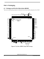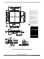
1
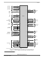
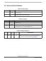
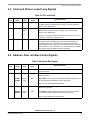
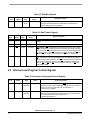
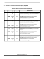
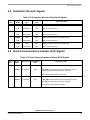
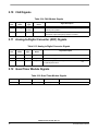
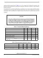
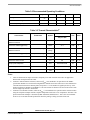
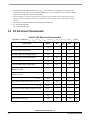
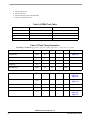
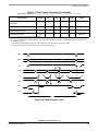
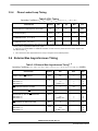
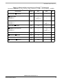
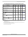
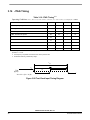
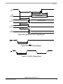
2.10 CAN Signals
Table 2-14 CAN Module Signals
No. of
Pins
Signal
Name
Signal
Type
State During
Reset
1
MSCAN_ RX
Input
(Schmitt)
Input
1
MSCAN_ TX
Output
Output
Signal Description
MSCAN Receive Data—This is the MSCAN input. This pin has an
internal pull-up resistor.
MSCAN Transmit Data—MSCAN output. CAN output is
open-drain output and a pull-up resistor is needed.
2.11 Analog-to-Digital Converter (ADC) Signals
Table 2-15 Analog to Digital Converter Signals
No. of
Pins
Signal
Name
Signal
Type
State During
Reset
4
ANA0–3
Input
Input
ANA0–3—Analog inputs to ADC channel 1
4
ANA4–7
Input
Input
ANA4–7—Analog inputs to ADC channel 2
1
VREF
Input
Input
VREF—Analog reference voltage for ADC. Must be set to VDDA-0.3V
for optimal performance.
Signal Description
2.12 Quad Timer Module Signals
Table 2-16 Quad Timer Module Signals
No. of Pins
Signal Name
Signal Type
State During Reset
2
TD1–2
Input/Output
Input
Signal Description
TD1–2— Timer D Channel 1–2
56F803 Technical Data, Rev. 16
16
Freescale Semiconductor