1
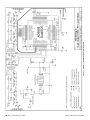
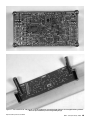
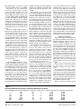
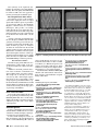
Thomas M. Alldread, VA7TA
7056 Railway Ave, Courtenay, BC V9J 1N4, CANADA; [email protected]
NimbleSig III
—Part 1
Build this dual output DDS
RF generator and low-level RF
power meter.
This article describes the design and construction details for a stable, frequency agile,
dual output, direct digital synthesizer (DDS)
based RF signal generator module with a built
in RF level meter. This module is intended to
be used as a building block to provide the
signal source and RF level measurement
functions for many possible applications
such as signal generators, swept frequency
spectrum displays, receivers, transmitters
and RF modems. It could provide both
local oscillator signals for a dual conversion
receiver or a pair of frequency locked signals
for applications that require a quadrature
phase offset local oscillator signal pair. The
signal outputs can be described as frequency
agile as they can be altered very quickly by
command without any settling time requirement. The output frequencies can be independently set with 1 Hz resolution anywhere
within the 100 kHz to 200 MHz range. The
firmware provides an ASCII command line
type interface, which enables control directly
from a PC equipped with suitable serial port
interface. Any conventional terminal program that supports 115,200 Baud (such as
HyperTerminal) is all that is needed for the
PC software to establish keyboard control of
the dual DDS and signal level meter. When
used as a building block for more complex
applications control could be provided by
any dedicated host microcontroller that has a
UART peripheral capable of 115 KBaud and
that is programmed to send the necessary
commands to the NimbleSig module.
During the past decade and a half I have
been following the development of DDS
technology and have designed and built
about a dozen DDS generators. My first
DDS generator had a relatively low clock
rate of 50 MHz, which limited the maximum
output frequency to about 20 MHz. I built
it, along with an analog to digital converter
(ADC), on a wire-wrapped ISA card that
Reprinted with permission © ARRL
filled a whole slot in my then state of the art
486 based PC. I controlled the DDS/ADC
chips directly from the ISA computer bus
with an application I dubbed “PanaBand,”
which was written in the PASCAL language.
Figure 1 is an example of the PanaBand full
screen, VGA, color graphics display (considered high resolution in the early 1990s)
that shows the IF output frequency spectrum from my HF transceiver. In addition to
the frequency spectrum display PanaBand
also provided GUI style mouse and point
and click control of my transceiver via the
serial port interface. The ability to view the
frequency and strength of all the signals on
the selected HF band with digital display
accuracy and to also be able to tune to any
one of them with just a “click of the mouse”
seemed pretty wonderful in the early 1990s.
Although my old PanaBand project will not
be described here it is an example of what can
be done with DDS technology when placed
under computer control. The seemingly
open-ended realm of possible applications
associated with computer controlled DDS
signal sources hooked me on further experimentation with this technology.
My first version of this series of DDS
signal source designs only provided a single
output up to 160 MHz. It also provided AM/
FM modes and had a built in RF level meter.
It used a 32 bit, 50 MHz ARM microcontroller with 64 KB of program memory
space. To my very pleasant surprise, that
project won second place in the Luminary
Micro Inc sponsored “Design Stellaris 2006”
international design competition, which was
hosted by Circuit Cellar Magazine.1
NimbleSig III (NS3), described here, is
my most recent DDS module design. It is
relatively enhanced in that it provides two
independent RF signal outputs with 1 Hz frequency step resolution up to 200 MHz. Either
generator output can be AM/FM modulated
at specified modulation indexes at rates from
1 Hz to 20 kHz. Alternately each RF generator can be simultaneously set to the same
frequency to provide a pair of signals with
accurate relative phase offsets. These offsets
can be changed in very fine steps across the
full 360° range. The built in RF power meter
can measure levels with typical 1 dB accuracy from –50 to +10 dBm from just above
the audio spectrum to about 500 MHz.
NS3 uses a relatively recent DDS chip
from Analog Devices Incorporated (ADI),
which is clocked at 500 MHz. The 50 MHz,
ARM7 NXP (formally Philips) controller
used here has 512 KB of program memory
space. This large instruction code space provides room for many enhancements to the
firmware as only about 20% of the program
memory space is currently used. Also new
in this version is a 64 KB EEPROM, which
is provided for non-volatile (NV) storage of
internal initialization and calibration data. A
1
Notes appear on page 20.
QEX – January/February 2009
3
Figure 1 — A Kenwood TS-850S transceiver IF spectrum display, based on early 1990s DDS technology.
Figure 2 — The NimbleSig III block diagram illustrates the main sections of the circuit.
4
QEX – January/February 2009
Reprinted with permission © ARRL
16 KB block of this NV memory space is
allocated for storing external host controller
application data such as initialization values
and frequency channel information.
As shown in the lead photo, modern
surface mount technology makes it possible to fit all the functionality and power of
NimbleSig III into a very small (2 × 3 × 0.5
inch) package.
Hardware
Block and Level Diagram
As shown in the Figure 2 block diagram,
the reference clock for the MPU is provided
by the internal 25 MHz, FOX 924, temperature-controlled crystal oscillator (TCXO)
IC, which by optional default also provides
the reference clock for the DDS. Both the
DDS and MPU have internal phase lock
loops that are programmed to multiply the
clock reference input to the actual internal
clock frequency, which, as mentioned in the
introduction, is 50 MHz for the MPU and
500 MHz for the DDS.
At room temperature the TCXO provides good enough frequency stability for
many DDS applications. Using my relatively
stable oven-controlled crystal oscillator
(OCXO) referenced frequency counter, I
have observed a day-to-day variation of less
than 10 Hz when operating continuously at
100 MHz within a room-temperature controlled environment.
Although the TCXO provides quite a
respectable degree of stability it may not
be sufficiently stable for applications that
are critically frequency dependent or where
the DDS cannot be left powered up for a
long enough lead time to stabilize. Also, the
DDS internal PLL, which in the case of the
TCXO operation is set to multiply the reference clock frequency by 20, has the disadvantage of significantly increasing the phase
noise. The DDS data sheet indicates a phase
noise improvement of about 20 dB can be
obtained by driving the clock input directly
with a 500 MHz, low phase noise reference
signal. Although I believe the TCXO/PLL
combination is more than adequate for most
applications much better phase noise performance should be possible if an external, low
sideband noise, high overtone crystal oscillator (such as the Butler type) is used to drive a
suitable multiplier to obtain a relatively quiet
500 MHz, 1 mW clock source.
As shown in the upper left of Figure 2,
an external clock signal may be optionally
injected for the DDS frequency reference.
The maximum drive amplitude is 1.4 V p-p
into a 50 Ω load, which, considering a sine
wave source, works out to about 5 mW or
+7 dBm. The DDS specification states the
injection level should be in the range of –5
Reprinted with permission © ARRL
to +3 dBm (2 mW). The external input is
directly terminated in 50 Ω and the clock is
subsequently capacitive coupled to the DDS
input, which floats on an internally generated
dc bias.
The ADI AD9958 IC has a pair of internal
DDS engines, which use the clock signal as a
reference to generate sine wave output signals
on frequencies specified by data stored in the
associated internal registers. The AD9958 is
described in detail within the manufacturer’s
data sheet.2 A great deal of information on
the theory of DDS signal generation, including an Amateur Radio related project (AN557) can be found within Analog Devices’
library of DDS application notes.3
The DDS receives data and control signals from the MPU. The register data for
setting the operating mode, frequency, phase
and amplitude is sent serially via a high
speed, 25 Mb/S, serial peripheral interface
(SPI) bus. There are 3 control registers containing, in total, 6 bytes of data common to
both DDS engines. In addition data is stored
for each individual engine by 21 dedicated
registers containing 82 bytes of channel
specific information that includes frequency,
amplitude and relative phase offset values.
The SPI bus consists of four lines, namely
“master input/slave output”(MISO) data,
“master output/slave input”(MOSI) data,
“serial clock”(SCLK) and “slave select”(SS).
The MPU acts as the master and the DDS
the slave. Details of the general operation of
the SPI bus can be found on the Internet (see
Note 4) and more specific information on the
SPI format used for this application can be
found within the DDS data sheet (see Note
2) and the MPU users manual.4, 5
There are nine additional control lines
connecting the DDS and MPU that have
various functions including chip select,
DDS reset, DDS power control, register data
update strobe and modulation step selection.
The two RF outputs from the DDS, which
contain both the desired output signals and
the undesired images, are fed into seven
pole, elliptic design type, low pass filters that
strip off the images and any other out of band
signals. These image regions, which extend
from 300 MHz to 750 MHz and beyond,
are attenuated by a minimum of 50 dB by
the filters.
The RF output levels are set to –10 dBm
with frequency dependent amplitude calibration data that is stored within the EEPROM
by the calibration subroutines. This data is
sent to the DDS by the MPU each time a
new frequency command is implemented.
The output levels may be reduced by command in 0.1 dB steps to –20 dBm. It is also
possible to bypass the calibration and operate at unleveled, full output, which is about
–4 dBm mid spectrum.
The RF level detector is designed around
the popular, broadband AD8307 logarithmic
response power detector IC from ADI. It has
a bandwidth specification of dc to 500 MHz.
The variable dc output from the detector is
connected to one of the 10 bit analog-todigital converter inputs of the MPU.
The RF detector IC has a significant
response roll off between HF and UHF.
Calibration data to compensate for this frequency roll off along with correction data for
the device dependent logarithmic response
variations is stored within the EEPROM during calibration. If the approximate frequency
(specified in units of MHz) is supplied with
the power measurement command, the
level reading is adjusted for the frequency
specified. Also during calibration, data
from a curve fitting algorithm that matches
the dynamic range response of the specific
logarithmic detector IC is also saved in
EEPROM.
As shown in the block diagram the
EEPROM data is conveyed to and from the
MPU via an Inter-Integrated Circuit (I2C –
for “I squared C”) bus. Details on the general
operation of the I2C bus can also be found
on the Internet.6 More specific information
on the protocol for this application can be
found in Microchip’s 24LC512 EEPROM
data sheet.7
A UART peripheral within the MPU provides the 115,200 Baud, ASCII serial data
communications link to the outside world.
The data on the receive data (RXD) and
transmit data (TXD) lines is in the positive
3.3 V, unipolar format typically found on
3.3 V microcontroller I/O pins. This simple
logic level interface was selected as it offers
both direct compatibility to a host controller
microprocessor as well as indirect compatibility to either USB or legacy RS-232 serial
port PC interfaces. Although this interface
requires either an RS-232C level conversion
or USB protocol conversion device to interface to a standard personal computer it was
chosen as it provides the most universal fit
for all perceived applications. The RXD and
TXD MPU pins are protected from induced
transients or other abnormal line conditions
with 1K resistors.
Two LEDs are provided to indicate status
of the MPU. A red LED, designated RST,
illuminates when the MPU reset line is pulled
low to force the MPU to the reset state. A
green LED, designated HEART, flashes at
72 PPM to indicate the firmware is executing. These indicators are not important to the
normal operation of the module but can save
a lot of time during programming, troubleshooting and debugging by indicating rather
vague operational status “at a glance”.
Six additional I/O lines make up the
“Joint Test Action Group” (JTAG) bus,
QEX – January/February 2009
5
Figure 3 — Section 1 of the NimbleSig III schematic diagram.
6
QEX – January/February 2009
Reprinted with permission © ARRL
which is used for programming and debugging the software. These lines terminate on a
SIP connector that provides connection to the
software development system for programming and debugging.
The LPC2138 MPU used here is a variant of ARM Incorporated’s ARM7 family
manufactured by NXP (previously Philips)
Semiconductors. The ARM 7 family of 32
bit MPUs are relatively powerful processors
in comparison to the 8 bit microcontrollers
more commonly seen in amateur radio
projects. The ARM 7 is clocked roughly 10
times faster, processes 4 bytes at a time and
in this case has more than 10 times the program memory space normally found in 8 bit
MPU chips. One of the primary reasons for
the use of an ARM processor is that it is well
supported by software development tools
that provide 64-bit arithmetic to calculate
the DDS 32-bit frequency tuning words on
the fly, which for this application, eliminates
rounding error.
The extra MPU power and memory space
also provides the foundation for a plain text,
command line style, man/machine interface.
There is an abundance of storage room for
help pages, register dump tables and calibration routines. The firmware has commands
that provide the user full access to read or
write to any of the DDS registers. The user is
also given the power to change the DDS initialization values without the need to reprogram the MPU (The user may revert back to
the original default parameters for recovery
if needed).
A very important consideration for the
use of the LPC2138 MPU is that there are
good quality and affordable integrated development environment (IDE) software tools
available to write and maintain the software
for this family of ARM processors. Rowely
Associates’ Crossworks for ARM, which
uses the well proven GNU GCC C compiler, was used to develop the NS3 firmware.
Rowely Associates offer a non-commercial,
hobbyist/student level license for this fully
functional (not crippled or limited), professional quality, well supported IDE package
at a much reduced price that is within reach
of most serious radio amateur equipment
builders.8
Considering all the advantages of the
ARM processor the additional cost of just a
few dollars over a more common 8 bit processor chip seems, in the author’s opinion,
well justified.
The two, dual output voltage power
regulators shown in Figure 2 play a very
important role in this design. Experience
has proven that noise on the power rails is a
major problem for DDS generators. If digital
noise gets superimposed on the analog voltage bus to the DDS, noise sidebands of sigReprinted with permission © ARRL
nificant level can appear across the spectrum.
Also any noise on the TCXO power causes
FM sidebands to appear. The most effective
means for obtaining clean power for a DDS
generator is by isolating the analog/digital
buses from each other with dedicated voltage regulators. Fortunately, semiconductor
manufacturers have introduced low cost, dual
output voltage regulators in small packages
that serve this need nicely. Separate voltage
supply rails with dedicated regulators are
provided here for the 3.3 V digital devices,
3.3 V TCXO supply, 1.8 V DDS digital supply and 1.8 V DDS analog supply. Power for
the regulators is supplied from an external,
regulated +5 V dc supply. The +5 V source
passes through a low forward voltage drop,
reverse polarity protection diode prior to distribution to the regulator inputs.
Circuit Description
The first schematic sheet shown in Figure
3 shows the details of the AD9958 DDS and
analog power regulator circuitry.
The various ground and power bus designators are shown at the lower left of the
page. As shown there are four separate
ground planes, namely, analog ground,
digital ground, filter 0 ground and filter 1
ground. These ground planes are isolated
from each other by PC board design. This
design approach helps prevent the coupling
of digital noise into the analog circuitry and
crosstalk between the generator outputs that
could otherwise be caused by noise voltage
gradients on a relatively simplistic, single
ground plane.
The +5 V dc power input (center – left) is
first routed through a Schottky diode that provides reverse polarity protection with only
about a 0.4 V forward voltage drop. The diode
output of 4.7 V supplies the RF Detector and
the regulator inputs. The LP2966 dual output voltage regulators are of the ultra low
voltage drop-out type. With the provided
1.3 V headroom, these devices have sufficient control margin to provide well regulated
3.3 V outputs.
The 4.7 V power bus is bypassed with
a 0.1 µF bypass capacitor (C27) to guard
against possible RF noise superimposed on
the 5 V power source. The power passes
through a 1 Ω resistor (R5) that provides
a small amount of low frequency isolation
between the analog and digital grounds. This
resistor also provides a convenient point to
check the analog regulator input current.
The load side of R5 feeds an RF bead that
provides an impedance to RF current flow
between the analog and digital grounds. C30,
a tantalum input filter capacitor, provides a
low impedance bypass of the analog regulator IC input to analog ground. As shown,
the 1.8 V and 3.3 V regulator outputs are
bypassed by two additional tantalum electrolytic capacitors (C31, C32). As the 3.3 V
output only powers the TCXO, it operates
with a light load of approximately 5 mA. In
contrast the 1.8 V output feeds the DDS analog bus, which is a relatively heavy load of
around 100 mA.
The functions of the common components
connected to the AD9958 DDS are described
in Table 3, “Pin configuration and Function
Descriptions” within the device datasheet
given at the reference of Note 2. The 16 connections between the DDS and the MPU
are shown entering a bus that reappears on
sheet 2. Balanced lines on the PC board
connect the push-pull RF outputs from the
DDS to the associated transformer-coupled
low pass filters. These balanced lines help
prevent crosstalk between generator outputs.
The transformer coupling isolates the filter
grounds and provides efficient push-pull
coupling of RF from the DDS outputs to
the filter inputs. Power for the DDS DAC
outputs is injected into the primary center
taps of the transformers. Resistors R1, R2,
R3 and R4 moderate the out of band impedance extremes presented to the DDS outputs,
which if not moderated would cause excessive intermodulation distortion from image
products. Capacitors C9 and C10 are RF
bypasses for the center tap power injection
points. A detailed description of the low pass
filter design is given below.
Figure 4 is the schematic for the MPU,
TCXO, EEPROM, digital power regulator
and RF detector circuitry. The 3.3 V and
1.8 V digital power is supplied from the dual
digital power regulator U4. R9 provides a
small amount of power decoupling from the
4.7 V bus and also provides a convenient test
point for measurement of the input current to
the regulator. Tantalum electrolytic capacitors C42, C43 and C44 ensure regulator stability. The 1.8 V output load is 60 to 80 mA.
The 3.3 V output load that supplies the MPU,
EEPROM and RF level detector is estimated
to be less than 50 mA.
As shown in the upper left of the diagram
3.3 V digital power is injected into pins 23,
43, 49 and 51 of the MPU. RFB2 and C41
provide decoupled injection of this power to
the analog ADC reference voltage pin 7.
R10 and R11 are current limiting resistors
for the indicator LEDs. R15, 18, 19, 22, 23,
24, 26, 25 and R18, 19, 20 are logic pull-up
and pull-down resistors respectively.
C51 couples the 3.3 V p-p, 25 MHz
square wave reference clock from the TCXO
output to the XTAL1 clock injection pin of
the MPU. R16 and 17 form a voltage divider
to drop the amplitude to 1.4 V p-p for injection into the DDS. Note that if the external
reference clock option is desired, R16 is
omitted and R17 is changed to 51 W for
QEX – January/February 2009
7
Figure 4 — Section 2 of the NimbleSig III schematic diagram.
8
QEX – January/February 2009
Reprinted with permission © ARRL
terminating the external clock signal source.
The external signal connection point is the
high end of R17.
R12 and R13 form a voltage divider to
drop the 3.3 V logic level output from the
MPU GPIO P30.0 pin to match the 1.8 V
logic level of the DDS clock mode select
input.
The TXD and RXD pads provide connection points for the ASCII data communications connection to the host computer. R7
and 8 protect the MPU RXD, TXD internal
interface circuitry from direct exposure to
outside connection, extraneous voltages and/
or shorts to ground.
The power to the 64KByte EEPROM,
U3 is bypassed by C40. The power to the RF
level detector U5 is decoupled by ferrite bead
RFB3 and bypassed with tantalum capacitor
C46. C48 bypasses the RF from the detector
output, yet provides a fast enough response
time to measure audio modulation envelope
peaks. C47 and 49 couple the input RF to
the detector from the 51 W input termination R14.
The JTAG programming/debugging
interface connector consists of a 10 pin,
0.010 inch pitch, machined quality, goldplated SIP socket connector strip. This was
selected as a commonly available, space
efficient, low profile alternative to the usual
20 pin header used for ARM JTAG interfacing for which there was insufficient mounting space. A simple adapter board has been
designed to convert to the 20 pin standard.
The operation of the JTAG interface is complex and black magic to the author. There
is much JTAG information available on the
web but as I have found the JTAG operation
to be transparent I decided there would be little practical benefit for me to learn the details
of the operation of this complex interface. I
can say it works wonderfully well!
Elliptic Low Pass Filters
Figures 5 and 6 show the schematic and
simulated response of the 200 MHz LPF.
The parallel resonant circuit traps comprised
of L1/C3 [L6/C8], L2/C4 [L5/C7] and L3/
C5 [L4/C6] provide rejection nulls in the stop
band at 300, 250 and 500 MHz respectively.
The 250 MHz notch was chosen to establish
the corner of the stop band at the half clock
frequency. The 300 MHz null provides the
needed attenuation for the “500 MHz clock
minus output frequency” lower sideband
image that is present when the DDS is used
to generate frequencies close to 200 MHz.
Image signals would otherwise appear as
spurious outputs. As described within ADI’s
application note AN-939, the level of the
image sidebands will taper off towards the
500 MHz clock frequency.9 The combination
of the Nyquist level tapering effect and rejecReprinted with permission © ARRL
tion of the filters for all intents and purposes
eliminate the image signals.
The Elliptic LPF design, which is based
on ADI’s application note AN-837, was
designed using two freeware software packages.10 Tonne Software’s SVC Filter Designer
was used to do the preliminary design and
Linear Technology’s LTCSpice program was
used to analyze the design.11, 12 This design
uses parallel pairs of capacitors for the shunt
capacitance elements to help ensure a low
RF impedance connection to the associated
LPF ground plane at UHF. All the frequency
determining components are SMD packagesize category 0402. With measurements of
only 0.4 mm × 0.2 mm, these components
are indeed quite small!
The roll off of the filter frequency response
in conjunction with the roll off of output level
from the DAC at the upper end of the first
Nyquist zone limits the leveled –10 dBm
output amplitude maximum frequency to
approximately 195 MHz. (See Note 9.) At
200 MHz the maximum output level drops to
about –12 dBm. Possibly the 200 MHz filter
loss could be reduced slightly with higher
Q inductors and/or shifting the LPF cutoff
frequency slightly higher. At the time of this
writing, I plan to re-design the LPF corner
frequency to around 230 MHz with the first
notch at 300 MHz instead of 250 MHz. The
need for establishing deep attenuation at
250 MHz is questionable considering the
lowest-frequency, full-level image product would be at 300 MHz. This re-design
may slightly reduce the attenuation in the
195-200 MHz region. If I find the modification provides a worthwhile performance
improvement I will post the design details on
my Web page.13
Assembly Description
Figure 7 is a close up view of the component side of the fully populated PCB
mounted into the chassis. The largest chip,
Figure 5 — Elliptic low pass filter schematic with parts list.
Figure 6 — Simulated LPF frequency response.
QEX – January/February 2009
9
Figure 7 — This photo shows the component side of the populated NimbleSig III circuit board.
mounted left of center, is the LPC2138 MPU.
The next largest chip in the upper center is the
AD9958 DDS. The small chip in the metal
case located above the MPU is the TCXO.
The AD8307 RF power detector is mounted
right of center at the bottom close to the RF
input connector. To the right of the detector is
the input protection diode, D1. The 24LV512
EEPROM is the chip above D1. The two
remaining small ICs are the LP2966 dual
output voltage regulators. The red LED reset
indicator is above the top left corner of the
MPU and the green LED heart beat indicator
is below the opposite corner.
The JTAG connector is to the left of
the MPU. Although the silkscreen labeling
seems to indicate otherwise please note that
pin 1 is actually at the top of the connector
just below the “JTAG” silkscreen label. The
PCB silkscreen labeling on this first manu-
10
QEX – January/February 2009
facturing run of PC boards is disrupted by
the vias, which are not covered by silkscreen.
The vias were intentionally left uncovered
to provide connection points for testing the
prototype. The labeling should be easier to
read in the future, if I have another batch of
boards made with the vias covered with the
silkscreen.
The frequency determining components
for the two low pass filters are located along
the opposite ends of the PCB between the RF
transformers (white blocks) and the output
connectors (shown with RF cables attached).
The three, tightly spaced, central SMB
connectors, left-to-right, provide the TXD,
RXD and RF IN (level meter input) external
connections. The power input is bypassed
and anchored to a ground lug under the RF
input connector. The power passes through
the chassis via an RF bead that serves as a
feed through insulator and provides some
RF isolation. A boot formed from hot glue
provides insulation for the power connections and strain relief for the cable. Although
the glue is rather messy, it has proven effective for protecting these connections and the
power cable.
With the exception of the JTAG connector
all components are of the surface mount type.
As mentioned above 0402 size components
are used for the filters. With a few exceptions
the rest of the ceramic capacitors and resistors are the larger 0603 size.
The components shown were hand
soldered under an 8X power binocular
microscope using a fine tip, 290°C, temperature-controlled pencil soldering iron with
0.015 inch (28 AWG) Kester 63/37 RA core
solder. Any excess solder was sopped up with
the 0.025 inch desoldering braid. For the first
Reprinted with permission © ARRL
step before installing any components I used
a flux pen manufactured by Kester to coat all
the PCB connections with flux. I also used
the flux pen to coat the contacts on the pinless
DDS chip, which made soldering this package much easier.
I wish to mention that until I was introduced to surface mount construction techniques about 5 years ago I avoided projects
based on surface mount devices. Now having experience with surface mount design
and construction I avoid the use of leaded,
through hole components where possible.
The ability to construct with surface mount
devices has opened up many project horizons
for me. I would also like to mention, how-
ever, that this project would be a poor choice
for one’s first attempt at surface mount construction. Some of the components used here
are very small and others have fine pin spacing. This project is intended for those with a
reasonably good collection of surface mount
construction tools and the acquired skill set to
use them proficiently.
My preferred sequence for manually soldering components to a board is to build and
test the regulated power supplies first. I then
install the the passive components whilst
routinely checking with my trusty, continuity
buzzer equipped Ohmmeter for power bus
shorts as I go along. Finally I mount the signal ICs leaving the relatively precious DDS
chip for the last. I check for any grounded
power supply buses after installing each IC.
Using this method one can usually find the
cause of an accidental power bus short fairly
quickly. Since typical power buses have wide
distribution trouble shooting a shorted bus
after all the components are installed can
be very difficult due to the maze of shorted
connection point possibilities. I also usually
take the time to check for adjacent pin shorts
with my Ohmmeter before applying power.
The use of a low test voltage Ohmmeter with
a continuity buzzer that provides the ability
to test for adjacent pin shorts without taking
your eyes away from the finely spaced leads
is a big asset for this job. To avoid false posi-
Figure 8 — The component side of the circuit board is shown in Part A. Part B shows the bottom of the circuit board.
Reprinted with permission © ARRL
QEX – January/February 2009
11
tives from device internal protection diodes,
it is important that the test voltage, imposed
by the continuity meter probes, is well below
0.5 V. Fortunately the continuity buzzer feature provided in most modern day digital
multimeters meet this requirement.
The PCB is a relatively simple doublesided board compared to the relatively expensive four-layer board type usually specified
for DDS applications. The four-layer boards
more readily provide low RF impedance
ground planes. The two-layer board used
here provides the requisite low impedance
analog ground via a large ground post, which
connects the analog ground pad of the DDS
chip direct to the chassis. Additionally, there
are four isolated ground planes provided by
the artwork design, which are bonded at the
chassis connector apron. This design significantly reduces the coupling of noise and
crosstalk between circuit sections.
Figure 8A shows the component side
of the PCB artwork. The large, 0.125 inch
diameter plated through hole in the center
of the DDS footprint provides access from
underneath for soldering the analog ground
center pad of the DDS chip. This facilitates
the installation of the DDS chip using a conventional soldering iron. The author has had
a 100% success rate using an inexpensive
soldering iron with a blunt, 0.100 inch diameter tip that has been filed flat. The soldering iron is adjusted to 280°C with a Variac
transformer. A small coil of solder is inserted
in the hole and the soldering iron tip inserted
into the hole, branding iron style, for 5 seconds or less. This does a good job of soldering the DDS pad to analog ground and also
provides a good contact area for the analog
ground post.
The balanced lines that couple the push
pull outputs from the DDS to the respective
low pass filter input transformers can be seen
along the top edge of the PCB. As mentioned
above, the maximum separation of the filters
along with the balanced lines helps provide
good isolation between the generator outputs. The exposure to the coupling of stray
RF noise into the RF level meter input from
the rest of the circuitry is minimized by the
placement of the “RF_IN” pad right beside
the detector chip input pin.
Figure 8B shows the bottom side of the
PCB artwork, which shows the four distinct
ground planes. The analog ground post connection to the ground pad of the DDS is the
large plated through hole under the DDS
chip. Analog ground wings extend under
the balanced lines to the underside of the
LPF transformer primary connections. The
analog ground also extends below the DDS
under the analog power regulator to the large
analog ground pad near the center bottom
of the photo. The two filter grounds extend
from underneath the connections to the
transformer secondaries to the corresponding
filter ground pads near the bottom corners of
the board. The digital ground extends from
the left side of the DDS down to the very bottom and across to the RF detector, EEPROM,
digital voltage regulator and JTAG connector
areas. The digital and analog grounds are
connected together with a zero Ohm resistor located near the RF detector. The ground
pads are ultimately bonded by soldering to
Figure 9 — Grounding braid bonds the circuit board grounds to the coaxial SMB connectors.
12
QEX – January/February 2009
Reprinted with permission © ARRL
Figure 10 — Part A shows the analog ground post. Part B shows the tapped hole for the analog ground post.
Reprinted with permission © ARRL
QEX – January/February 2009
13
the outer conductor threads of the coaxial
connectors.
The board is mounted to the chassis by
soldering the component side pads to the
respective connector center pins and by
bonding the ground pads on the bottom side
of the board with braid to the connector
threads as shown in Figure 9. A large soldering iron with lots of thermal mass is needed
for soldering to the threads. Do not use a
soldering gun for this job as the magnetic
field from the tip may induce destructive currents into the semiconductor circuitry. The
back of the board rests on the analog ground
post shown in Figure 10. The tip of the brass
screw is covered with a blob of solder to
provide a soft contact surface with good galvanic compatibility. The chassis cover shown
in Figure 11 has a bumper made up from
commonly available, self-adhesive rubber
feet. This somewhat resilient bumper presses
against the top of the DDS chip holding it
firmly against the ground post.
The reason for providing the ground post
is to lower the RF impedance of the analog
ground by providing a low Z path via the relatively large chassis surface area to the bonding point for the multiple grounds at the RF
connectors. The PCB analog ground plane
copper area would by itself provide sufficient
heat sinking for the DDS chip without the
presence of the ground post. As the AD9958
runs with a relatively low, 1.8 V core voltage,
this chip does not dissipate nearly as much
power as some of the earlier DDS devices
that required better cooling. Thus depending
on the mechanical design of the enclosure a
chassis ground connection alternative to the
ground post such as a short length of flexible
grounding braid or other low RF impedance
path to the chassis could be used. Use caution
if soldering to the ground post pad, because it
would be quite easy to overheat and possibly
destory the DDS chip, which is thermally
coupled to the pad.
The square corners of the PCB, which are
intended to be trimmed off to fit the surplus
die cast aluminum chassis used here, can be
used with standoffs to provide an alternative
mounting method. As shown in Figure 12,
photos A and B, there is just enough room
to drill 3/32 inch holes for 2-56 machine
screw hardware. Note that the holes need
to be drilled with a degree of precision and
although not shown here the use of nylon
screws and insulating washers is necessary
to ensure the board ground planes remain
electrically isolated from the chassis.
The PCB artwork shown here is the first
revision, in which the majority of the first
run problems were corrected. For this revision of the board, however, there remains
the need for two, easy-to-install jumpers and
if desired, a test point to simplify entry into
the internal system programming mode. The
errata details are available on my Web site.
(See Note 13.) If there is sufficient interest
these items will be corrected for the next
manufacturing run of boards.
Performance Test Results
Frequency Spectrum Purity
Obtaining a clean spectrum from a DDS
generator is somewhat of a design challenge and thus is also rewarding to achieve.
Spectrum purity tests are consequently high
on the priorities list for proof of performance.
Since both the DDS and MPU chips are digital devices, if all is not well with the circuit
design and layout, the spectrum can become
polluted with unwanted spurs at significant
levels. As illustrated by the array of spectrum analyzer photos in Figure 13, the signal
from NimbleSig III is very clean. In order to
display the full 200 MHz spectrum with the
noise floor sufficiently low to reveal the spurs
my legacy spectrum analyzer was pushed to
its limits. It was necessary to increase the
sweep duration to 100 seconds for most of
the tests. The adjustment of the baseline clipper was quite critical and a good compromise
between the high intensity needed to clearly
paint the narrow spurs, prevention of variable persistence storage blooming, viewing
of the noise floor while retaining readability
of the text fonts proved to be tedious. Please
note that the center frequency readout text
field data of 0000 MHz, which appears in
all of the Figure 13 photos, is caused by a
malfunction in the logic circuitry within my
spectrum analyzer. This is just a problem
with the readout circuitry, which fortunately
does not affect the fundamental performance
of the analyzer. I hope to someday obtain
the triple connector card extender I need to
troubleshoot this logic circuit.
The photos across row 1 show the full
200 MHz spectrum with output frequencies,
from left to right, of 10, 20, 40 and 50 MHz.
As shown, most spurs are greater than 60 dB
down from the carrier. Note that the 50 MHz
example has the highest spur of the group at
100 MHz. As this spur drops down with just
a slight shift of carrier frequency, I wonder if
this spur is made worse when the output carrier is a direct sub multiple of the reference
clock frequency.
The row 2 photos are also full 200 MHz
spectrum sweeps. Photos A2 and B2
both show the carrier frequency set to
103.333 MHz, but the reference clock source
differs. In photo A2 the DDS was running
with the PLL set to 20:1 multiplication using
the internal 25 MHz TCXO as the reference. In photo B2 the PLL was disabled with
the DDS locked to an external, 500 MHz
injected reference. Clearly, as one would
expect, the spectrum is cleaner with the DDS
Figure 11 — This is the DDS chip compression bumper, as described in the text.
14
QEX – January/February 2009
Reprinted with permission © ARRL
Figure 12 — Part A shows the no. 2-56 machine screws for mounting the circuit board. Part B shows the no. 2-56 tapped mounting standoffs.
— Note: use nylon standoffs to preserve the grounding design.
Reprinted with permission © ARRL
QEX – January/February 2009
15
PLL disabled. Photos C2 and C3 are a similar
comparison with the output set to 146 MHz.
The photos in row 3 are relatively narrow, higher resolution displays intended
to show modulation and phase noise. The
DDS output carrier frequency was set to
103.333 MHz. From left to right the spans
are 5 kHz, 10 kHz, 20 kHz and 200 kHz with
resolution bandwidths of 30 Hz, 300 Hz,
300 Hz and 3 kHz respectively. Thanks
mainly to the grounding scheme and the use
of multiple power regulators these photos
illustrate that the DDS signal is free of any
significant periodic noise modulation, which
would otherwise appear as symmetrical sidebands.
The lower, straight baseline in photo C3
illustrates the spectrum analyzer noise floor
with the input disconnected. This test was
a somewhat inconclusive attempt to illustrate the phase noise whilst running from an
external 500 MHz reference. The external
500 MHz reference source was provided by
a signal generator based on a PLL synthesizer as opposed to a low phase noise source,
which would have been a better choice. The
contribution to the phase noise from the signal generator to the measurement done here
was not determined. I hope to pursue the
phase noise testing using a known low noise
500 MHz signal source for the reference and
a filter to prevent analyzer overload in the
future. I think it is fair to say that the noise
performance of this DDS design looks good
enough to justify pursuing a wider dynamic
range measurement.
Modulation
Both AM and FM, variable rate, sinusoidal audio modulation modes are provided
within NimbleSig III. Either RF output may
be modulated but simultaneous modulation of both outputs is not supported. The
modulation rate can be varied from 1 Hz to
20 kHz. The amplitude modulation depth can
be varied from 1% to 99%. The power-onreset defaults are set at 400 Hz and 30%. The
FM deviation can be set in 1 Hz steps from
10 Hz to 100 kHz, with defaults set at a rate
of 400 Hz with 3 kHz deviation. In the case
of the AM mode, the RF output amplitude is
dropped by 6 dB to provide headroom for the
modulation envelope peaks. Thus, during the
AM mode, the calibrated average RF output
level from the generator drops from –10 to
–16 dBm.
The modulation process increments and
decrements the amplitude or frequency in discrete, sinusoidally defined steps that simulate
a pure sine wave modulation tone. The step
definitions, either amplitude or frequency,
are calculated in advance after the user enters
the desired modulation frequency, along with
either the amplitude modulation percentage
or frequency modulation deviation values.
For modulation frequencies below 1.5 kHz
the step definition data is stored within the
MPU RAM. The MPU sends this data on
a repetitive basis to the DDS, step-by-step,
during modulation to shift either the DDS
output amplitude or frequency depending
on the mode. For higher modulation rates
(above 1.5 kHz) the pre-calculated step data
is stored in advance within internal DDS registers (called profile registers). The internal
modulation capability of the DDS is then
used under the control of the MPU to impose
the higher rate RF carrier modulation.
The modulation scheme used provides
finer resolution as the modulation rate
decreases. The number of steps used for
modulation frequencies below 1.5 kHz is
limited by the total time it takes to send the
data for defining the next step to the DDS
plus the execution time of the modulation
interrupt service routine (ISR). Table 1 illustrates how the audio spectrum is broken up
into seven segments, in which the number of
steps per cycle varies from 180 down to 30 as
the modulation frequency is increased.
For modulation frequencies of 1.5 kHz
and lower a timer interrupt that is assigned
a high priority in the MPU vector interrupt
controller (VIC) is used to update the DDS
registers with new step definition data. This
data is sent just prior to each modulation
step via the high speed (25 Mb/s) SPI interface. As previously mentioned modulation
frequencies above 1.5 kHz use the internal
modulation mode of the AD9958 DDS.
This mode, which is limited to a maximum
30 steps per cycle resolution, offers a higher
modulation rate capability as the data for
each step is preloaded into internal DDS reg-
isters. This eliminates the need for sending
definition data for each step on a real time
basis when the modulation is running. The
steps are selected via the dedicated, paralleladdress-style profile register selection bus,
which the MPU can update with just a single
general-purpose IO operation. The fast interrupt (FIQ) mode of the LPC2138 MPU
along with a short (13 machine instructions),
assembler code interrupt service routine
(ISR) work together when triggered by the
modulation rate timer to update the profile
register selection address. The MPU achieves
very fast speed in FIQ mode by marching in
and out of the very short ISR with minimal
overhead. The minimal overhead is facilitated by dedicated FIQ mode registers provided within the MPU, which eliminate the
traditional need for doing push/pops to/from
the stack during entry/exit to/from an ISR
Amplitude Modulation
Figure 14 is a photo array that illustrates
the amplitude modulation characteristics of
NimbleSig III. Row 1 illustrates how the
number of amplitude steps per cycle vary
inversely with the modulation rate. This
technique provides very fine steps for the
lower modulation rates, which optimizes
the shape of the modulation envelope for
the commonly used THD test frequencies.
Additionally it minimizes the amplitude of
the sampling spurs and helps keep the sampling frequencies well above the audio band
for all but very low modulation rates. The
sampling resolution is divided into seven
bands. Table 1 lists the seven audio band
segments with the associated step resolution
and rates.
Row 2 consists of the frequency domain
spectrum displays of the time domain
modulation envelopes in the photos directly
above.
Photos E1, E2 and E3 in Figure 14 illustrate the performance of the internal modulation feature of the AD9958. Although the
DDS internal modulation is limited to a resolution of 30 steps per cycle, the modulation
envelope remains well defined and also very
low in distortion. The in-band spurs are more
than 50 dB down from the carrier.
Figure 14, photos A3 and B3 are photos
Table 1
NimbleSig III Modulation Resolution for Different Modulation Rate Bands
Lower Band Edge (Hz) Upper Band Edge (Hz) Steps/Cycle Degrees/Step
1
250
180
2
251
400
120
3
401
500
90
4
501
800
72
5
801
1000
60
6
1001
1500
36
10
1501
20,000
30
12
16
QEX – January/February 2009
Minimum Step Rate (Hz) Maximum Step Rate (Hz)
180
45,000
30,000
48,000
36,090
45,000
36,072
57,600
48,060
60,000
36,036
54,000
45,030
600000
Reprinted with permission © ARRL
Figure 13 — NimbleSig III spectrum purity tests.
Reprinted with permission © ARRL
QEX – January/February 2009
17
18
QEX – January/February 2009
Reprinted with permission © ARRL
Figure 14 — NimbleSig III amplitude modulation envelope and frequency spectrum displays.
of the 20 Hz modulation envelope. These
photos are noteworthy because the step rate
of 3,600 Hz falls well within the audio spectrum. As shown, the step rate sidebands are
about 46 dB below carrier, which would be
about 40 dB below the 20 Hz sidebands (not
visible here). Although it is unlikely that this
characteristic would affect typical receiver
testing, operators performing very low
modulation frequency tests should expect
the presence of very low amplitude (-40 dB
or lower) step rate frequency related tones
within the audio spectrum.
Figure 14, photos C3 and E3 show wider
views of the spectrum during modulation. As
shown the splatter level is about –55 dBc at
the 1 kHz rate and –42 dBc at the 10 kHz rate.
I believe the microprocessor IO transient
delays are responsible for the higher splatter
at 10 kHz. The transients are just barely visible in photo E1.
I provided photo D3 in Figure 14 to provide some perspective to the quality of the
NimbleSig III modulation performance. D3
is the spectrum photo from my late 1990s
technology, high end (about $8000 new),
industrial quality, commercial signal generator. As shown the second harmonic modulation sidebands are about 30 dB below the
fundamental sidebands. This converts to a
total harmonic distortion of a little more than
3%, which is within the generator specification of maximum 4% THD.14 As shown by
Photo C3, the NimbleSign III AM distortion
sidebands are about 20 dB lower than the
second order sidebands of my commercial
signal generator. It is apparent from this that
the THD performance of the digital modulation method used here should be less than
0.5% considering the bandwidth restrictions
of a typical AM receiver.
A downside of the digital modulation used
by NS3, which is usually of no consequence
for receiver testing, is that there are relatively
high frequency, moderate level sampling
rate sidebands generated by the encoding
step transitions. These sidebands appear in
the frequency spectrum at multiples of the
sample rate around the carrier as shown in
Figure 14 photo B3 for 20 Hz modulation
(discussed above regarding audible spurs
for very low frequency modulation rates).
The amplitudes of these spurious sidebands
decrease as the order of the sidebands
increase and also decrease as the modulation steps are made finer. The closest, most
significant, first order sideband pair will be at
least 30 kHz away from the carrier (except in
the case of very low modulation rates, where
the amplitude of the spurs would be relatively
low because of the finer steps). The spurs are
usually of no concern, because they are well
beyond the bandwidth of the typical communications receiver, which normally would
not pass these sampling rate sidebands. If the
device under test happens to have more than
30 kHz of bandwidth, such as receivers used
for video or high speed data, the digital modulation spurs could appear within the baseband spectrum after the detector at a worst
case amplitude of about 5% of the voltage of
the modulation signal. Thus, those who wish
to use NS3 for modulation related applications should be aware that modulation spurs
could be present in broadband applications.
The amplitude of the modulation sampling rate sidebands could be greatly reduced
if the modulation steps could be sloped
to approximate the sine wave shape. The
AD9958 does provide a feature for shap-
ing the step transitions for digital modulation where the step sizes are all the same.
Unfortunately, I was unable to adapt this
feature for sinusoidal modulation, as the step
sizes vary.
Frequency Modulation
The frequency spectrum display of an
FM signal is useful for viewing the transfer
of carrier power into the sidebands as the
deviation is increased from zero. When the
peak deviation is set to approximately 2.4
times the modulation frequency ( modulation index = 2.4028) all the signal power
is shifted into the sidebands and the carrier power literally drops to near zero. This
carrier drop out phenomenon commonly
referred to as 1st Bessel zero is very useful
for checking deviation accuracy and purity
of modulation.15
Figure 15 is a photo array of first Bessel
zero nulls (modulation index of 2.4048)
obtained for modulation rates between
100 Hz and 20 kHz in a 1-2-5 sequence. This
provides insight to the NS3 FM modulation
performance and deviation setting accuracy.
The deep Bessel function carrier nulls are
shown near the center of the photos. The
depth of these nulls, which are very deep
considering the logarithmic display, is a good
indicator of quality of tone, tone frequency
and deviation accuracy. A degradation of any
of these qualities would prevent a deep Bessel
zero carrier dropout. Since the NS3 DDS
frequency step resolution is 0.116 Hz
(500 MHz / 232 ) both the the relative frequency of the modulation steps and the peak
deviation are accurately controlled. This level
of accuracy could be useful for checking the
calibration of deviation meters.
Figure 15 — Bessel zero FM modulation frequency spectrum displays at various modulation rates
Reprinted with permission © ARRL
QEX – January/February 2009
19
The symmetry of the significant sidebands is also an indicator of good modulation
linearity. The tonal quality of the FM should
be similar to AM as the same approach is
used for generating the modulation signal.
Dual Output Relative Phase Offset
The AD9958 provides 14 bit resolution
control of the output phase of the two output
signals. This results in a phase step resolution
of approximately 0.02197°. The NimbleSig
III phase command values are entered in
millidegrees. This provides a reasonably
human-friendly data entry method that effectively harnesses the fine resolution steps with
minimal rounding error. The commands will
be described in more detail in Part 3 of this
article.
A unique command is provided that loads
the same frequency simultaneously into both
generators, and in the process locks the output signals together with a defineable phase
offset. Oscilloscope photo A1 of Figure
16 shows the waveforms from the two RF
outputs operating in phase while photo B1
illustrates the cancellation of the two signals
when added together with one oscilloscope
channel inverted. The Figure 16, A2 and B2
photos show the two signals with a 180,000
and 90,000 millidegree offsets respectively.
Power Detector Modes
The NS3 design permits RF level measurement from a single sample, or the average level from either 128 or 1024 consecutive
samples.
Additional commands permit the detection of the maximum or minimum level
detected during 1024 consecutive samples.
The sample rate is currently set for once
every 56.3 µs, thus a 1024 sample sequence
takes about 58 ms. Consequently, a 1024
sample sequence spans sufficient time to capture the maximums and minimums of an AM
signal modulated at a 20 Hz rate. This feature
can be used to measure peak envelope power
or percentage of modulation.
Parts 2 and 3 to Follow
Part 2 of this article will describe the software, programming and initial testing of the
NimbleSig III module. Part 3 of this article
will describe the NS3 command set in detail,
calibration procedures and a mouse button
control program.
Acknowledgments
I wish to acknowledge many discussions
with Jim Koehler, VE5FP, who deserves much
credit. Jim is currently developing a signal generator that is based on the NS3 module.
I wish to thank Analog Devices Inc for
their development of the fine RF integrated
circuits on which NimbleSig III is based. I
20
QEX – January/February 2009
Figure 16 — Relative generator A / B controlled phase offset time domain oscilloscope views.
wish to thank Rowely Associates (in particular Mr. Paul Curtis) for their excellent
CrossWorks for ARM development tools
product and for their solid support, which
enabled me to bring the development of the
NS3 firmware to a successful conclusion.
I would also like to thank the ARRL QEX
editorial staff and Technical Advisors for
their assistance in the finalization and publishing of this article.
Notes
NimbleSig winning entry URL: www.
circuitcellar.com/designstellaris2006/
winners/1648.html.
2
ADI AD9958 data sheet URL: www.analog.
com/static/imported-files/data_sheets/
AD9958.pdf.
3
ADI DDS application notes: www.analog.
com/en/DCcList/0,3090,770%255F%255F
43,00.html.
4
SPI Bus: en.wikipedia.org/wiki/Serial_
Peripheral_Interface_Bus.
5
LPC2138 User’s Manual: www.standardics.
nxp.com/support/documents/
microcontrollers/pdf/user.manual.
lpc2131.lpc2132.lpc2134.lpc2136.
lpc2138.pdf.
6
I2C Bus: en.wikipedia.org/wiki/I2c.
7
Microchip 24LC512 datasheet: ww1.
microchip.com/downloads/en/
DeviceDoc/21754E.pdf.
8
Rowley CrossWorks for ARM: www.rowley.
co.uk/arm/.
9
DDS Nyquist Images: www.analog.com/en/
rfif-components/direct-digitalsynthesis-dds/products/applicationnotes/resources/index.html.
1
LPF Design Reference: www.analog.
com/UploadedFiles/Application_
Notes/351016224AN_837.pdf.
11
Filter Design Software: www.tonnesoft
ware.com/.
12
LTSpice Simulation Software: www.linear.
com/designtools/software/switchercad.
jsp.
13
NimbleSig III Web page: www3.telus.net/ta/
NimbleSig%20III/.
14
THD Measurement and Conversion: www.
dogstar.dantimax.dk/tubestuf/thdconv.
htm.
15
Frequency Modulation: en.wikipedia.org/
wiki/Frequency_modulation.
10
Tom Alldread, VA7TA, became interested in
electronics when still in grade school, repaired
radio and television sets in his teens, obtained
his Amateur Radio ticket at the age of 19, and
went on to obtain commercial radio operator certification a year later. He subsequently
graduated from the Capitol Radio Engineering
Institute Engineering Technology program. His
career was in the telecommunications industry
where he worked in microwave and VHF radio
equipment maintenance, training, engineering
standards and design, and long distance network operations management.
Tom is now retired and lives on Vancouver
Island with his wife Sylvia, VA7SA. Tom has
a history in repeater building and emergency
communications, and he enjoys operating
mobile CW, building equipment and is currently the net manager for the 20 meter Trans
Canada Net. His other interests include microcontroller programming, circuit design, computing, hobby farming, digital photography,
bicycling and sailing.
Reprinted with permission © ARRL