1
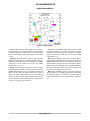
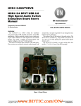
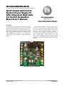
NCV8855BMNR2GEVB
Quad-Output Automotive
System Power Supply IC
with Integrated High-Side
2 A Switch Evaluation
Board User's Manual
http://onsemi.com
EVAL BOARD USER’S MANUAL
Introduction
The NCV885x is intended to supply power to various
loads, such as a tuner, CD logic, audio processor and CD /
tape control within a car radio. The high-side switch can be
used for a CD / tape mechanism or switching an
electrically-powered antenna or display unit. In an
instrument cluster application, the NCV885x can be used to
power graphics display, flash memory and CAN
transceivers. In addition, the high-side switch can be used to
limit power to a TFT display during a battery overvoltage
condition.
The NCV885x is a multiple output controller / regulator
IC with an integrated high-side load switch. The NCV885x
will address automotive radio system and instrument cluster
power supply requirements. In addition to the high-side load
switch, the NCV885x comprise a switch-mode power
supply (SMPS) buck controller, a 2.5 A SMPS buck
regulator, and two low dropout linear regulator controllers
(LDO).
Figure 1. NCV8855 Evaluation Board
© Semiconductor Components Industries, LLC, 2012
May, 2012 − Rev. 1
1
Publication Order Number:
EVBUM2120/D
NCV8855BMNR2GEVB
Table 1. EVALUATION BOARD TERMINAL DESCRIPTIONS
Terminal
Function
VBATT
Positive dc input voltage.
VOUT1
Synchronous SMPS regulated dc output voltage.
VOUT2
Nonsynchronous SMPS regulated dc output voltage.
VOUT3
LDO regulated dc output voltage.
VOUT4
LDO regulated dc output voltage.
HS_S
HOT_FLG
HS_EN
High Side Switch output.
Thermal warning indicator. Provides an early warning of impending thermal shutdown.
Enable pin for the high-side load switch. A logic high on this pin will enable the HSS. If this pin is left floating, an internal pull down keeps the HSS disabled.
LDO_EN
Enable pin for both LDO controllers. A logic high on this pin will enable both LDO controllers. If this pin is left floating,
an internal pull down keeps the LDOs disabled.
SYS_EN
Main enable pin for the IC. A logic high on this pin will enable the part. Leaving this pin floating or driving it to ground
will place the IC in shutdown mode.
SYNC
Synchronization pin. Use this pin to synchronize the internal oscillator to an external clock.
GND
Common DC return.
Table 2. ABSOLUTE MAXIMUM RATINGS (Voltages with Respect to GND)
Rating
DC Supply Voltage (VBATT)
DC Supply Voltage (HS_EN, LDO_EN, SYS_EN, SYNC)
Value
Unit
−0.3 to 30
V
−0.3 to 7
V
Junction Temperature (NCV8855)
−40 to 150
°C
Ambient Temperature (Evaluation board)
−40 to 105
°C
Stresses exceeding Maximum Ratings may damage the device. Maximum Ratings are stress ratings only. Functional operation above the
Recommended Operating Conditions is not implied. Extended exposure to stresses above the Recommended Operating Conditions may affect
device reliability.
http://onsemi.com
2
NCV8855BMNR2GEVB
JUMPER EXPLANATION
Figure 2. Jumper Groups
Green: VOUT2 (SMPS2) output voltage selection. With
no jumper VOUT2 is 3.3 V. With a jumper between the
middle pin and the pin labeled 5 V, VOUT2 is 5 V. With a
jumper between the middle pin and the pin labeled
8 V, VOUT2 is 8 V.
Red: VOUT4 (LDO2) input source selection. With a
jumper between the middle two pins, the input to VOUT4 is
VBATT. With a jumper between the middle pin and the pin
labeled VOUT2, the input to VOUT4 is VOUT2. With a
jumper between the middle pin and the pin labeled VOUT1,
the input to VOUT4 is VOUT1 (The selected voltage must
be at least 5 V to ensure proper function).
Blue: VOUT1 (SMPS1) output voltage slection. With no
jumper VOUT1 is 3.3 V. With a jumper between the middle
pin and the pin labeled 5 V, VOUT1 is 5 V. With a jumper
between the middle pin and the pin labeled 8 V, VOUT1 is
8 V.
Cyan: VOUT3 (LDO1) output voltage selection. With no
jumper VOUT3 is 1.2 V. With a jumper between the middle
pin and the pin labeled 3.3 V, VOUT3 is 3.3 V. With a jumper
between the middle pin and the pin labeled 2.5 V, VOUT3
is 2.5 V.
Magenta: VOUT4 (LDO2) output voltage selection.
With no jumper VOUT4 is 5 V. With a jumper between the
middle pin and the pin labeled 6 V, VOUT4 is 6 V. With a
jumper between the middle pin and the pin labeled
8.5 V, VOUT4 is 8.5 V.
Yellow: VOUT3 (LDO1) input source selection. With a
jumper between the middle two pins, the input to VOUT3 is
VBATT. With a jumper between the middle pin and the pin
inline with the other pin labeled VOUT2, the input to
VOUT3 is VOUT2. With a jumper between the middle pin
and the pin inline with the other pin labeled VOUT1, the
input to VOUT3 is VOUT1 (The selected voltage must be
at least 5 V to ensure proper function).
http://onsemi.com
3
NCV8855BMNR2GEVB
APPLICATION DIAGRAM
DRV_VPP
SYS _EN
22
5
Bandgap
ILIMIT
V1
5V_IC
VIN
DRV_VPP
VIN
VR
VIN
Q1 GH1
SN1
VOUT1
Q2 GL1
OCSET
LDO
11
24
23
21
QS
CLK1
CLK2
QR
R
9
ILIMIT
EA
29
30
RAMP1
70%
VREF
SCP
DRV_VPP
EA
3
CLK1
RAMP1
CLK2
RAMP2
OSC
180°
out−of−phase
5V_IC
UVLO
HOT_FLG
8
TWARN1
TWARN2
ISNS1+
VOUT1
ISNS1−
VOUT3
Q3
LR_G1
LR_FB1
6
Int. rails
and
references
TSD2
ILIMIT
39
EA
EA
38
HS_OUT
VIN
HS_S
26
28
33
34
SCP
70% VREF
VBATT
31
ILIMIT
V REF
SCP
70% VREF
VIN
Control
Current
Limit
Vneg
clamp
37
CLK1
Vhigh
clamp
20
AGND
PGND
Figure 3. Application Diagram
http://onsemi.com
4
VBATT
SN2
VOUT2
SW_FB2
COMP2
SYNC
HS_EN
LDO_EN
5V_IC
32
VREF
1
4
7
Main Logic / Fault
Control
TSD1
40
VIN_SW
D1
2
SCP
BST2
V REF
RAMP2
27
DRAIL
SS2
ILIMIT
V REF
COMP1
10
S Q
SS1
SW_FB1
36
25
Gate Control
VBATT
5V_IC
I LIMIT
V1
VR
BST1
35
Charge
Pump
ISNS2+
VBATT
ISNS2−
LR _G2
LR_FB2
Q4
VOUT4
NCV8855BMNR2GEVB
TEST PROCEDURE
Equipment Needed
Changing the Switcher Output Voltage
Power Supplies (1 High Power, 1-3 Logic Level)
Digital Volt Meter
Digital Ampere Meter
Function Generator (optional)
12. Remove the SYS_EN voltage
13. Connect a jumper in the Vout1 (to change the
Vout1 voltage) or Vout2 (to change the Vout2
voltage) areas between the middle pin labeled
3.3 V and the pin labeled 5 V (to change the output
5 V) or the pin labeled 8 V (to change the output
voltage.
14. Reapply the SYS_EN voltage
15. The output should now be around the set voltage.
The current consumption from VBATT will
increase if the output voltage is increased.
Set-up
1. Remove jumpers from Vout 1, Vout 2, Vout 3, and
Vout 4 voltage select jumpers.
2. Set the ISNS1+ and ISNS2+ jumpers to the middle
positions (VBATT)
3. Set the high power supply to 13.2 V and a current
limit of at least 1.5 A.
4. Connect VBATT to the positive end of the power
supply and the adjacent GND to the negative end
of the power supply.
5. The DC current on VBATT should be around 6 mA
LDO Test
16. With the SYS_EN connected to a power supply,
connect the LDO_EN pin to a power supply in the
same voltage range in a similar fashion.
17. Vout3 should be around 1.2 V and Vout 4 should
be around 5 V.
Switcher Test
6. Set one of the logic level power supplies to a
voltage between 2.0 V and 5.5 V.
7. Connect SYS_EN to the positive end of the power
supply and a GND pin to the negative end of the
power supply.
8. Switcher 1 and 2 will turn on. Switcher 2 includes
a minimum load of 340 W to ensure continuous
conduction mode switching. The DC current on
VBATT should be around 37 mA.
9. The Vout1 and Vout2 should be around 3.3 V.
Changing the LDO Output Voltage
18. Remove the LDO_EN Voltage (optionally the
SYS_EN voltage as well)
19. Add a jumper between the middle pin and the
desired output voltage in the area around the
respective outputs to change the voltage. (Note:
Vout4 has a pin that may appear to be labeled
3.5 V due to overlapping a via. Actually this sets
the output voltage to 8.5 V)
High Side Switch Test
Synchronize the Switchers
20. With a SYS_EN powered as above, measure the
voltage on HS_S with respect to GND. This
should be around 0 V.
21. Connect the HS_S pin to a power supply in the
same voltage range and in a similar fashion to the
SYS_EN voltage.
22. Measure the voltage on HS_S with respect to
GND. This should be around VBATT.
10. Set the function generator to a square wave with
logic low 0.0-0.8 V and logic high 2.0-5.5 V with
frequency 190-255 kHZ.
10. Connect the positive end of the function generator
to the SYNC and the negative end to GND.
11. VSW1 will synchronize to the rising edge and
VSW2 will synchronize to the negative edge of the
square wave.
http://onsemi.com
5
NCV8855BMNR2GEVB
TYPICAL WAVEFORMS
Figure 4. VOUT1 (5 V) and VOUT2 (3.3 V), start up
with 340 W load on both
Figure 5. VOUT4 (5 V) and VOUT3(1.2 V), start up
with no load
Figure 6. VOUT1 (5 V) and VSW1, 4 A load
Figure 7. VOUT2 (3.3 V) and VSW2, 2 A load
Figure 8. High Side Switch Turn On
Figure 9. High Side Switch Turn Off
http://onsemi.com
6
1.2 V
3.3 V
RFB2
1.74k
JB2
CV12 RV12
1nF
15.0k
CV22 2.2nF
RF02
3.24k
RF12
10.2k
RF13
5.11k
Q2
NTD20P06L
MOS_DPAK
TP4
RO21
OPEN
TP10
LDO1
RO22
OPEN
C8
47uF
VOUT3
RS1
150m
J4
VOUT4 1
J3
VOUT2 1
C15
330uF
VOUT2
1
TP14
L2
33uH
5V_IC
TP17
0
J8
SYNC
2
BST2
COMP2
SW_FB2
ROSC
SYNC
SYS_EN
LDO_EN
HS_EN
HOT_FLG
SN2
VIN_SW
BST2
U2
NCV8855
48LQFP
C21
1
LR_G1
2
COMP2
3
SW_FB2
4
ROSC
5
SYS_EN
6
LDO_EN
7
HS_EN
8
HOT_FLG
9
SN2
10
VIN_SW
D1
MBRS4201T3G
0.1uF
C10
TP8
J9
VOUT1 J10
VOUT2
R16
10.0k
TP9
TP7
VIN
R18
SMPS2
TP11
C4
0.47uF
TP1
R17
OPEN
For QFN parts with SYNC option,
populate R18 with 0 Ohm,
unpopulate R17.
ROSC
J2
2
2
2
2
VOUT31
RFA2
4.87k
JA2
RF22
10.0
CF22
22nF
RF03 10.2k
J15
RFA3 1.96k
8 V
2.5 V
J16
RFB3 3.16k
5 V
C2 0.1uF
ISNS1+
ISNS1−
LR_FB1
AGND
DRAIL
5V_IC
LR_FB2
LR_G2
ISNS2−
ISNS2+
NCV8855
U1
41
40
39
38
37
36
35
34
33
32
31
1
2
3
4
5
6
7
8
9
10
11
12
0.1uF
11
12
13
14
15
16
17
18
19
20
TN5
TN2
TN1
PGND
30
29
28
27
26
25
24
23
22
21
J6
J7
TP3
LDO2
TP2
C1
0.47uF
3.3nF
10.5k
RF14
TN4
TN3
TN5
TN2
TN1
36
35
34
33
32
31
30
29
28
27
26
25
OPEN
OPEN
OPEN
BGRAIL
COMP1
SW_FB1
V0P8
HS_S
OCSET
VIN
BST1
GH1
SN1
DRV_VPP
GL1
TP15
TP20
TP19
C18
0.47uF
C17
0.47uF
C19
0.47uF
VIN_SW
VPWR
VIN
Q4
NTD24N06L
MOS_DPAK
HSS
CV21
C3
47uF
VOUT4
Q1
NTD20P06L
MOS_DPAK
RS2
150m
C20
1500uF
2
3.3 V
CV11 1nF RV11 15.0k
COMP1
SW_FB1
HS_S
TP5
TP6
CF21
OCSET R8
10.0kVPWR
22nF
VIN
BST1
C9 0.1uF
Q3
RF21
GH1
NTD24N06L
10.0
SN1
MOS_DPAK L1
DRV_VPP
22uH
1
GL1
C11
0.47uF
0805
VOUT1
VOUT2
RT3
RT2
RT1
VIN
J5
RFB4 2.43k
VBATT
C12
330uF
VOUT1
RF11
10.2k
RF01
3.24k
RF04 2.00k
JA4 RFA4 8.45k
JB4
TP12
JA1
RFB1
1.74k
TP18
TP16
TP13
JB1
RFA1
4.87k
5 V
6 V
8.5 V
SMPS1
8 V
VOUT11
3.3 V
7
LR_G1
ISNS1+
ISNS1−
LR_FB1
AGND
DRAIL
5V_IC
LR_FB2
LR_G2
ISNS2−
ISNS2+
http://onsemi.com
48
47
46
45
44
43
42
41
40
39
38
37
Figure 10. Evaluation Board Schematic
13
14
15
16
17
18
19
20
21
22
23
24
5 V
J1
NCV8855BMNR2GEVB
SCHEMATIC
NCV8855BMNR2GEVB
Table 3. BILL OF MATERIALS
Part
Tolerance
PCB
Footprint
Substitution
Allowed
RoHS
Compliant
Part Description
Manufacturer
22nF
10%
603
CAP CER
22000PF 50V X7R
0603
Murata
Electronics North
America
GCM188R71H22
3KA37
YES
YES
CF22
22nF
10%
603
CAP CER
22000PF 50V X7R
0603
Murata
Electronics North
America
GCM188R71H22
3KA37
YES
YES
CV11
1nF
10%
603
CAP CER 1000PF
50V X7R 0603
Murata
Electronics North
America
GCM188R71H10
2KA37
YES
YES
CV12
1nF
10%
603
CAP CER 1000PF
50V X7R 0603
Murata
Electronics North
America
GCM188R71H10
2KA37
YES
YES
CV21
3.3nF
10%
603
CAP CER 3300PF
50V 10% X7R
0603
Murata
Electronics North
America
GRM188R71H33
2KA01D
YES
YES
CV22
2.2nF
10%
603
CAP CER 2200PF
50V 10% X7R
0603
Murata
Electronics North
America
GRM188R71H22
2KA01D
YES
YES
C1
0.47uF
10%
805
CAP CER .47UF
50V X7R 0805
Murata
Electronics North
America
GRM21BR71H47
4KA88L
YES
YES
C4
0.47uF
10%
805
CAP CER .47UF
50V X7R 0805
Murata
Electronics North
America
GRM21BR71H47
4KA88L
YES
YES
C11
0.47uF
10%
805
CAP CER .47UF
50V X7R 0805
Murata
Electronics North
America
GRM21BR71H47
4KA88L
YES
YES
C17
0.47uF
10%
805
CAP CER .47UF
50V X7R 0805
Murata
Electronics North
America
GRM21BR71H47
4KA88L
YES
YES
C18
0.47uF
10%
805
CAP CER .47UF
50V X7R 0805
Murata
Electronics North
America
GRM21BR71H47
4KA88L
YES
YES
C19
0.47uF
10%
805
CAP CER .47UF
50V X7R 0805
Murata
Electronics North
America
GRM21BR71H47
4KA88L
YES
YES
C2
0.1uF
10%
603
CAP CER .1UF
50V X7R 0603
Murata
Electronics North
America
GCM188R71H10
4KA57D
YES
YES
C9
0.1uF
10%
603
CAP CER .1UF
50V X7R 0603
Murata
Electronics North
America
GCM188R71H10
4KA57D
YES
YES
C10
0.1uF
10%
603
CAP CER .1UF
50V X7R 0603
Murata
Electronics North
America
GCM188R71H10
4KA57D
YES
YES
C21
0.1uF
10%
603
CAP CER .1UF
50V X7R 0603
Murata
Electronics North
America
GCM188R71H10
4KA57D
YES
YES
C3
47uF
20%
UD_6.3x
5.8
CAP 47UF 10V
ELECT UD SMD
Nichicon
UUD1A470MCL1
GS
NO
YES
C8
47uF
20%
UD_6.3x
5.8
CAP 47UF 10V
ELECT UD SMD
Nichicon
UUD1A470MCL1
GS
NO
YES
C12
330uF
20%
UD_8x10
CAP 330UF 10V
ELECT UD SMD
Nichicon
UUD1A331MNL1
GS
NO
YES
Reference
CF21
http://onsemi.com
8
Manufacturer’s
Part Number
NCV8855BMNR2GEVB
Table 3. BILL OF MATERIALS
Substitution
Allowed
RoHS
Compliant
UUD1A331MNL1
GS
NO
YES
Nichicon
UHE1H152MHD
NO
YES
DIODE
SCHOTTKY 4A
200V SMC
ON
Semiconductor
MBRS4201T3G
NO
YES
805
CONN HEADER
2POS .100 VERT
GOLD
Molex/Waldom
Electronics Corp
22-28-4024
YES
YES
N/A
805
CONN HEADER
2POS .100 VERT
GOLD
Molex/Waldom
Electronics Corp
22-28-4024
YES
YES
JUMPER
N/A
805
CONN HEADER
2POS .100 VERT
GOLD
Molex/Waldom
Electronics Corp
22-28-4024
YES
YES
JA2
JUMPER
N/A
805
CONN HEADER
2POS .100 VERT
GOLD
Molex/Waldom
Electronics Corp
22-28-4024
YES
YES
JB4
JUMPER
N/A
805
CONN HEADER
2POS .100 VERT
GOLD
Molex/Waldom
Electronics Corp
22-28-4024
YES
YES
JA4
JUMPER
N/A
805
CONN HEADER
2POS .100 VERT
GOLD
Molex/Waldom
Electronics Corp
22-28-4024
YES
YES
J5
JUMPER
N/A
805
CONN HEADER
2POS .100 VERT
GOLD
Molex/Waldom
Electronics Corp
22-28-4024
YES
YES
J6
JUMPER
N/A
805
CONN HEADER
2POS .100 VERT
GOLD
Molex/Waldom
Electronics Corp
22-28-4024
YES
YES
J7
JUMPER
N/A
805
CONN HEADER
2POS .100 VERT
GOLD
Molex/Waldom
Electronics Corp
22-28-4024
YES
YES
J8
JUMPER
N/A
805
CONN HEADER
2POS .100 VERT
GOLD
Molex/Waldom
Electronics Corp
22-28-4024
YES
YES
J9
JUMPER
N/A
805
CONN HEADER
2POS .100 VERT
GOLD
Molex/Waldom
Electronics Corp
22-28-4024
YES
YES
J10
JUMPER
N/A
805
CONN HEADER
2POS .100 VERT
GOLD
Molex/Waldom
Electronics Corp
22-28-4024
YES
YES
J15
JUMPER
N/A
805
CONN HEADER
2POS .100 VERT
GOLD
Molex/Waldom
Electronics Corp
22-28-4024
YES
YES
J16
JUMPER
N/A
805
CONN HEADER
2POS .100 VERT
GOLD
Molex/Waldom
Electronics Corp
22-28-4024
YES
YES
J1
SMB
N/A
SMB_CO
NN
CONN JACK RF
VERTICAL
PCMNT GOLD
Emerson Network
Power
Connectivity
Solutions
131-3701-261
YES
YES
Part
Tolerance
PCB
Footprint
Part Description
Manufacturer
330uF
20%
UD_8x10
CAP 330UF 10V
ELECT UD SMD
Nichicon
C20
1500uF
20%
PM_16x4
0
CAP 1500UF 50V
ELECT HE
RADIAL
D1
MBRS42
01T3G
N/A
SMC_DI
ODE
JB1
JUMPER
N/A
JA1
JUMPER
JB2
Reference
C15
http://onsemi.com
9
Manufacturer’s
Part Number
NCV8855BMNR2GEVB
Table 3. BILL OF MATERIALS
Manufacturer’s
Part Number
Substitution
Allowed
RoHS
Compliant
Emerson Network
Power
Connectivity
Solutions
131-3701-261
YES
YES
CONN JACK RF
VERTICAL
PCMNT GOLD
Emerson Network
Power
Connectivity
Solutions
131-3701-261
YES
YES
SMB_CO
NN
CONN JACK RF
VERTICAL
PCMNT GOLD
Emerson Network
Power
Connectivity
Solutions
131-3701-261
YES
YES
20%
WE_PD_
L
INDUCTOR
POWER 22UH
5.3A SMD
Wurth Electronics
Inc
7447709220
NO
YES
33uH
20%
WE_PD_
L
INDUCTOR
POWER 33UH
3.2A SMD
Wurth Electronics
Inc
744770133
NO
YES
Q1
NTD20P
06L
N/A
MOS_DP
AK
MOSFET PWR
P-CH LOG 15A
60V DPAK
ON
Semiconductor
NTD20P06LT4G
NO
YES
Q2
NTD20P
06L
N/A
MOS_DP
AK
MOSFET PWR
P-CH LOG 15A
60V DPAK
ON
Semiconductor
NTD20P06LT4G
NO
YES
Q3
NTD24N
06
N/A
MOS_DP
AK
MOSFET N-CH
60V 24A DPAK
ON
Semiconductor
NTD24N06LT4G
NO
YES
Q4
NTD24N
06
N/A
MOS_DP
AK
MOSFET N-CH
60V 24A DPAK
ON
Semiconductor
NTD24N06LT4G
NO
YES
RFA1
4.87k
1%
603
RES 4.87K OHM
1/10W 1% 0603
SMD
Vishay/Dale
CRCW06034K87
FKEA
YES
YES
RFA2
4.87k
1%
603
RES 4.87K OHM
1/10W 1% 0603
SMD
Vishay/Dale
CRCW06034K87
FKEA
YES
YES
RFA3
1.96k
1%
603
RES 1.96K OHM
1/10W 1% 0603
SMD
Vishay/Dale
CRCW06031K96
FKEA
YES
YES
RFA4
8.45k
1%
603
RES 8.45K OHM
1/10W 1% 0603
SMD
Vishay/Dale
CRCW06038K45
FKEA
YES
YES
RFB1
1.74k
1%
603
RES 1.74K OHM
1/10W 1% 0603
SMD
Vishay/Dale
YES
YES
RFB2
1.74k
1%
603
RES 1.74K OHM
1/10W 1% 0603
SMD
Vishay/Dale
YES
YES
RFB3
3.16k
1%
603
RES 3.16K OHM
1/10W 1% 0603
SMD
Vishay/Dale
CRCW06033K16
FKEA
YES
YES
RFB4
2.43k
1%
603
RES 2.43K OHM
1/10W 1% 0603
SMD
Vishay/Dale
CRCW06032K43
FKEA
YES
YES
RF01
3.24k
1%
603
RES 3.24K OHM
1/10W 1% 0603
SMD
Vishay/Dale
CRCW06033K24
FKEA
YES
YES
PCB
Footprint
Reference
Part
Tolerance
Part Description
Manufacturer
J2
SMB
N/A
SMB_CO
NN
CONN JACK RF
VERTICAL
PCMNT GOLD
J3
SMB
N/A
SMB_CO
NN
J4
SMB
N/A
L1
22uH
L2
http://onsemi.com
10
CRCW06031K74
FKEA
CRCW06031K74
FKEA
NCV8855BMNR2GEVB
Table 3. BILL OF MATERIALS
Substitution
Allowed
RoHS
Compliant
CRCW06033K24
FKEA
YES
YES
Vishay/Dale
CRCW060310K2
FKEA
YES
YES
RES 10.2K OHM
1/10W 1% 0603
SMD
Vishay/Dale
CRCW060310K2
FKEA
YES
YES
603
RES 10.2K OHM
1/10W 1% 0603
SMD
Vishay/Dale
CRCW060310K2
FKEA
YES
YES
1%
603
RES 2.00K OHM
1/10W 1% 0603
SMD
Vishay/Dale
CRCW06032K00
FKEA
YES
YES
5.11k
1%
603
RES 2.00K OHM
1/10W 1% 0603
SMD
Vishay/Dale
CRCW06032K00
FKEA
YES
YES
RF14
10.5k
1%
603
RES 10.5K OHM
1/10W 1% 0603
SMD
Vishay/Dale
CRCW060310K5
FKEA
YES
YES
RF21
10.0
1%
603
RES 10.0 OHM
1/10W 1% 0603
SMD
Vishay/Dale
CRCW060310R0
FKEA
YES
YES
RF22
10.0
1%
603
RES 10.0 OHM
1/10W 1% 0603
SMD
Vishay/Dale
CRCW060310R0
FKEA
YES
YES
RT1
OPEN
1%
603
YES
YES
RT2
OPEN
1%
603
YES
YES
RT3
OPEN
1%
603
YES
YES
Part
Tolerance
PCB
Footprint
Part Description
Manufacturer
3.24k
1%
603
RES 3.24K OHM
1/10W 1% 0603
SMD
Vishay/Dale
RF03
10.2k
1%
603
RES 10.2K OHM
1/10W 1% 0603
SMD
RF11
10.2k
1%
603
RF12
10.2k
1%
RF04
2.00k
RF13
Reference
RF02
Manufacturer’s
Part Number
R17
OPEN
1%
603
YES
YES
RO21
OPEN
1%
603
YES
YES
RO22
OPEN
1%
603
YES
YES
RS1
150m
1%
CC1512F
C
RES 0.15 OHM
0.75W 1% 1512
FC SMD
Caddock
Electronics, Inc.
CC1512FC-0.151%
YES
YES
RS2
150m
1%
CC1512F
C
RES 0.15 OHM
0.75W 1% 1512
FC SMD
Caddock
Electronics, Inc.
CC1512FC-0.151%
NO
YES
RV11
15.0k
1%
603
RES 15.0K OHM
1/10W 1% 0603
SMD
Vishay/Dale
CRCW060315K0
FKEA
YES
YES
RV12
15.0k
1%
603
RES 15.0K OHM
1/10W 1% 0603
SMD
Vishay/Dale
CRCW060315K0
FKEA
YES
YES
R8
10.0k
1%
603
RES 10.0K OHM
1/10W 1% 0603
SMD
Vishay/Dale
CRCW060310K0
FKEA
YES
YES
R16
10.0k
1%
603
RES 10.0K OHM
1/10W 1% 0603
SMD
Vishay/Dale
CRCW060310K0
FKEA
YES
YES
http://onsemi.com
11
NCV8855BMNR2GEVB
Table 3. BILL OF MATERIALS
Substitution
Allowed
RoHS
Compliant
CRCW06030000
Z0EA
YES
YES
Molex/Waldom
Electronics Corp
22-28-4363
YES
YES
CONN HEADER
36POS .100 VERT
GOLD
Molex/Waldom
Electronics Corp
22-28-4363
YES
YES
POST
CONN HEADER
36POS .100 VERT
GOLD
Molex/Waldom
Electronics Corp
22-28-4363
YES
YES
N/A
POST
CONN HEADER
36POS .100 VERT
GOLD
Molex/Waldom
Electronics Corp
22-28-4363
YES
YES
POST
N/A
POST
CONN HEADER
36POS .100 VERT
GOLD
Molex/Waldom
Electronics Corp
22-28-4363
YES
YES
TP15
POST
N/A
POST
CONN HEADER
36POS .100 VERT
GOLD
Molex/Waldom
Electronics Corp
22-28-4363
YES
YES
TP2
T POINT
S
N/A
TURRET
TERM SOLDER
TURRET .219”
.109”L
Mill-Max
Manufacturing
Corp.
2501-2-00-44-0000-07-0
YES
YES
TP3
T POINT
S
N/A
TURRET
TERM SOLDER
TURRET .219”
.109”L
Mill-Max
Manufacturing
Corp.
2501-2-00-44-0000-07-0
YES
YES
TP4
T POINT
S
N/A
TURRET
TERM SOLDER
TURRET .219”
.109”L
Mill-Max
Manufacturing
Corp.
2501-2-00-44-0000-07-0
YES
YES
TP5
T POINT
S
N/A
TURRET
TERM SOLDER
TURRET .219”
.109”L
Mill-Max
Manufacturing
Corp.
2501-2-00-44-0000-07-0
YES
YES
TP6
T POINT
S
N/A
TURRET
TERM SOLDER
TURRET .219”
.109”L
Mill-Max
Manufacturing
Corp.
2501-2-00-44-0000-07-0
YES
YES
TP10
T POINT
S
N/A
TURRET
TERM SOLDER
TURRET .219”
.109”L
Mill-Max
Manufacturing
Corp.
2501-2-00-44-0000-07-0
YES
YES
TP12
T POINT
S
N/A
TURRET
TERM SOLDER
TURRET .219”
.109”L
Mill-Max
Manufacturing
Corp.
2501-2-00-44-0000-07-0
YES
YES
TP13
T POINT
S
N/A
TURRET
TERM SOLDER
TURRET .219”
.109”L
Mill-Max
Manufacturing
Corp.
2501-2-00-44-0000-07-0
YES
YES
TP14
T POINT
S
N/A
TURRET
TERM SOLDER
TURRET .219”
.109”L
Mill-Max
Manufacturing
Corp.
2501-2-00-44-0000-07-0
YES
YES
TP16
T POINT
S
N/A
TURRET
TERM SOLDER
TURRET .219”
.109”L
Mill-Max
Manufacturing
Corp.
2501-2-00-44-0000-07-0
YES
YES
TP17
T POINT
S
N/A
TURRET
TERM SOLDER
TURRET .219”
.109”L
Mill-Max
Manufacturing
Corp.
2501-2-00-44-0000-07-0
YES
YES
Part
Tolerance
PCB
Footprint
Part Description
Manufacturer
0
5%
603
RES 0.0 OHM
1/10W 5% 0603
SMD
Vishay/Dale
TP1
POST
N/A
POST
CONN HEADER
36POS .100 VERT
GOLD
TP7
POST
N/A
POST
TP8
POST
N/A
TP9
POST
TP11
Reference
R18
http://onsemi.com
12
Manufacturer’s
Part Number
NCV8855BMNR2GEVB
Table 3. BILL OF MATERIALS
Reference
Tolerance
PCB
Footprint
Manufacturer’s
Part Number
Substitution
Allowed
RoHS
Compliant
Part Description
Manufacturer
TP18
T POINT
S
N/A
TURRET
TERM SOLDER
TURRET .219”
.109”L
Mill-Max
Manufacturing
Corp.
2501-2-00-44-0000-07-0
YES
YES
TP19
OPEN
N/A
POST
CONN HEADER
36POS .100 VERT
GOLD
Molex/Waldom
Electronics Corp
22-28-4363
YES
YES
TP20
OPEN
N/A
POST
CONN HEADER
36POS .100 VERT
GOLD
Molex/Waldom
Electronics Corp
22-28-4363
YES
YES
U1
NCV885
5
N/A
QFN406x
6
ON
Semiconductor
NO
YES
U2
OPEN
N/A
48LQFP
ON
Semiconductor
NO
YES
Part
http://onsemi.com
13
NCV8855BMNR2GEVB
LAYOUT PLOTS
Figure 11. Silk Screen Top
Figure 12. Copper Top
Figure 13. Silk Screen Bottom
Figure 14. Copper Bottom
ON Semiconductor and
are registered trademarks of Semiconductor Components Industries, LLC (SCILLC). SCILLC reserves the right to make changes without further notice
to any products herein. SCILLC makes no warranty, representation or guarantee regarding the suitability of its products for any particular purpose, nor does SCILLC assume any liability
arising out of the application or use of any product or circuit, and specifically disclaims any and all liability, including without limitation special, consequential or incidental damages.
“Typical” parameters which may be provided in SCILLC data sheets and/or specifications can and do vary in different applications and actual performance may vary over time. All
operating parameters, including “Typicals” must be validated for each customer application by customer’s technical experts. SCILLC does not convey any license under its patent rights
nor the rights of others. SCILLC products are not designed, intended, or authorized for use as components in systems intended for surgical implant into the body, or other applications
intended to support or sustain life, or for any other application in which the failure of the SCILLC product could create a situation where personal injury or death may occur. Should
Buyer purchase or use SCILLC products for any such unintended or unauthorized application, Buyer shall indemnify and hold SCILLC and its officers, employees, subsidiaries, affiliates,
and distributors harmless against all claims, costs, damages, and expenses, and reasonable attorney fees arising out of, directly or indirectly, any claim of personal injury or death
associated with such unintended or unauthorized use, even if such claim alleges that SCILLC was negligent regarding the design or manufacture of the part. SCILLC is an Equal
Opportunity/Affirmative Action Employer. This literature is subject to all applicable copyright laws and is not for resale in any manner.
PUBLICATION ORDERING INFORMATION
LITERATURE FULFILLMENT:
Literature Distribution Center for ON Semiconductor
P.O. Box 5163, Denver, Colorado 80217 USA
Phone: 303−675−2175 or 800−344−3860 Toll Free USA/Canada
Fax: 303−675−2176 or 800−344−3867 Toll Free USA/Canada
Email: [email protected]
N. American Technical Support: 800−282−9855 Toll Free
USA/Canada
Europe, Middle East and Africa Technical Support:
Phone: 421 33 790 2910
Japan Customer Focus Center
Phone: 81−3−5817−1050
http://onsemi.com
14
ON Semiconductor Website: www.onsemi.com
Order Literature: http://www.onsemi.com/orderlit
For additional information, please contact your local
Sales Representative
EVBUM2120/D