1
Lecture 3: Sizing & Simulation
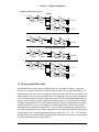
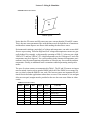
the load in a reasonable amount of time. If the fanout is small, the NOR might be sized
comparably to the NANDs. The path AF has wire, representing a fixed load. The inverter
driving the wire may see a load dominated by the wire, almost independent of the final
inverter size if the final inverter is not huge. The path is also irregular, because it is difficult
to decide how inverters I1 and I2 should be ratioed without information on the criticality
and delay of paths WB and WF. Finally, the path AG goes through non-critical logic.
Therefore, inverter I3 may be sized at minimum size to buffer the non-critical portion of
the circuit and minimize its load on the critical path. Thus, inverter I3 shows up as a fixed
side load.
FIGURE 1. Types of Side loads
A
I0
W
I1
X
I4
I8
AB: Main Path
B
C1
Side Loads:
I5
I9
C
C1
I6
I10
D
AC: Identical
AD: Proportional
C1
E
I7
I2
2 mm wire
I3
I11
Noncritical Logic
F
G
AE: Irregular
C1
C2 AF: Fixed &
Irregular
AG: Fixed
1.2 Identical Side Loads
Identical side loads are easy to deal with. Each contributes the same capacitance as the
main path. Therefore, a path with N-1 identical side loads can be sized as a single main
path with a logical effort N times larger. Then, the sizes of the original path are computed.
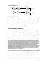
For example, the circuit in Figure 2 has an identical side load shown in part I. In part II, it
is lumped into a single path with twice the logical effort where the side load split off. The
total gain of the path is the total fanout times the total logical effort: (24/1)*1*10/3*1*1 =
80. Thus, the gain per stage is about the fourth root of 80, or 3. In part III, the equivalent
circuit is sized with a gain of about 3 per stage. In part IV, the original path is restored,
where the 10 units of capacitance on the combined gate is divided into 5 units on each
branch.
November 4, 1997
2 / 16