1
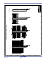
User´s Manual RH850 Evaluation Platform RH850/F1H 233-pin PiggyBack Board V1 32 RH850-F1X-233PIN-PB-T1-V1 All information contained in these materials, including products and product specifications, represents information on the product at the time of publication and is subject to change by Renesas Electronics Corp. without notice. Please review the latest information published by Renesas Electronics Corp. through various means, including the Renesas Technology Corp. website (http://www.renesas.com). www.renesas.com R20UT3227ED0100, Rev. 1.0 2014-11-18 Table of Contents Chapter 1 Introduction ......................................................................... 3 Chapter 2 Overview .............................................................................. 4 2.1 2.2 Overview ............................................................................................... 4 Mounting of the device ........................................................................ 5 Chapter 3 Power supply ....................................................................... 6 3.1 3.2 Board power connection ..................................................................... 6 Voltage distribution .............................................................................. 7 Chapter 4 Clock sources ...................................................................... 8 4.1.1 4.1.2 MainOsc .........................................................................................................................8 SubOSC .........................................................................................................................8 Chapter 5 Debug and Programming interface .................................... 9 Chapter 6 Connectors for ports of device......................................... 10 6.1 6.2 Push button for RESET ...................................................................... 10 Connectors to MainBoard .................................................................. 10 6.2.1 6.2.2 6.2.3 Connector CN1 ............................................................................................................10 Connector CN2 ............................................................................................................12 Connector CN3 ............................................................................................................13 Chapter 7 Mechanical dimensions .................................................... 15 Chapter 8 Schematic .......................................................................... 16 Chapter 9 Revision History ................................................................ 19 R20UT3227ED0100 Rev.1.0 2014-11-18 2 Chapter 1 Introduction The RH850/F1x Application Board is part of the RH850 Evaluation Platform and serves as a simple and easy to use platform for evaluating the features and performance of Renesas Electronics 32-bit RH850/F1x microcontrollers. The piggyback board (RH850-F1X-233PIN-PB-T1-V1) can be used as a standalone board, or can be mated with a mainboard (e.g. RH850-X1X-MB-T1V1) for extended functionality. Main features: Socket for mounting of device Standalone operation of the board Direct supply of device voltage (typ. 3.3V-5.0V) Device programming capability Device debugging capability Pin headers for direct access to each device pin Reset switch MainOSC and SubOSC circuitry Connectors to MainBoard This document describes the functionality provided by the piggyback board and guides the user through its operation. For details regarding the operation of the microcontroller, refer to the RH850/F1H User Manual. R20UT3227ED0100 Rev.1.0 2014-11-18 3 Chapter 2 Overview 2.1 Overview Figures 1 and 2 provide the views of the Piggyback Board. Device pin #A1 Figure 1 – PiggyBoard top view Figure 2 – PiggyBoard bottom view R20UT3227ED0100 Rev.1.0 2014-11-18 4 2.2 Mounting of the device The board is designed for use with the following devices: RH850/F1H-233 The device must be placed inside the socket IC1. To insert the device, press down the lid, align the #A1 pin of the device to the #A1pin of the socket, insert the device inside the socket and release the lid. R20UT3227ED0100 Rev.1.0 2014-11-18 5 Chapter 3 Power supply 3.1 Board power connection For operation of the device, a supply voltage must be connected to the board. Though a single supply voltage is sufficient for the operation of the device, two (different) voltages can be supplied to the board. Within this document the following voltages are considered as ‘typical’ connections: Voltage1 = 5.0V Voltage2 = 3.3V The following connectors are available to supply those voltages: Three 4mm ‘banana-type’ connectors: - Two red connectors for voltages Voltage1 (CN10) and Voltage2 (CN11). - A black connector for GND connection (CN12). Note: The three connectors are supplied with the board but not assembled. The E1 emulator that is used for debug purposes and flash programming can also supply a single operating voltage (‘Dbg_Voltage’). The voltage is programmable via the E1 GUI as 3.3 or 5.0V (typ). See the documentation of the E1 and chapter 5 ‘Debug and Programming interface’ for details. In case the PiggyBoard is mounted on a MainBoard, the voltages Voltage1 and Voltage2 are supplied by the on-board regulators of the MainBoard. NOTE: Do not supply any voltage directly to the PiggyBoard in case it is mounted on the MainBoard. For each of the two voltages, ‘Voltage 1 ‘ and ‘Voltage 2’, a green LED (LED1 and LED2) is available to signal that the related voltage is available on the PiggyBoard. R20UT3227ED0100 Rev.1.0 2014-11-18 6 3.2 Voltage distribution The table shows the required device power supply pins and their function: Device supply pin Function REGVCC Supply for the device internal regulators for the digital logic. EVCC Supply for ports. BVCC Supply for ports. A0VREF Supply for ports and analog functions of ADC0. A1VREF Supply for ports and analog functions of ADC1. For each of the above voltages, the voltage source can be selected from Voltage1 (typ. 5.0V) or Voltage2 (typ. 3.3V) by the jumpers JP0 and JP9. The IO supply voltage for the Mainboard can be selected via jumper JP7 from either the EVCC or the BVCC supply voltage. JP0 VOLTAGE1 JP9 JP4 VOLTAGE2 REGVCC JP5 JP7 EVCC VDDIOF JP1 BVCC JP3 A0VREF JP2 A1VREF R20UT3227ED0100 Rev.1.0 2014-11-18 7 Chapter 4 Clock sources Three external crystal oscillators for the device clock supply are provided with the board. 4.1.1 MainOsc A crystal or ceramic resonator in the range of 8MHz to 24MHz can be mounted on socket X1. A 8MHz and a 16Mhz oscillator is supplied with the board. 4.1.2 SubOSC An oscillator with a frequency of 32.768kHz is supplied with the board and can be soldered into the connector X2. R20UT3227ED0100 Rev.1.0 2014-11-18 8 Chapter 5 Debug and Programming interface For connection of the microcontroller debug and flash programming tools, the connector CN19 is provided. The signal connection of the connector CN19 is shown in the picture below: CN19 pin Device Port Device signal 1 JP0_2 DCUTCK / LPDCLK 2 GND GND 3 JP0_4 DCUTRST 4 FLMD0 FLMD0 5 JP0_1 DCUTDO / LPDO 6 - - 7 JP0_0 DCUTDI / LPDI 8 ‘Dbg_Voltage’ - 9 JP0_3 DCUTMS 10 - - 11 JP0_5 DCURDY / LPDCLKOUT 12 GND - 13 RESET - 14 GND - In case the FLMD1 signal must be controlled by the debug/programming tool, the pin header JP11 must be closed. The ‘Dbg_Voltage’ (on CN19 pin 8) is monitored or supplied by the debug and flash programming tools. Therefore, it is necessary to select either Voltage1 (5V) or the Voltage2 (3.3V) by pin header JP10: JP10 pin Selection for Dbg_Voltage 1-2 5V is selected 2-3 3.3V is selected R20UT3227ED0100 Rev.1.0 2014-11-18 9 Chapter 6 Connectors for ports of device Connection to each pin of the device is possible via the connectors CN5 to CN8. Note :The pin headers are directly connected to the pins, therefore special care must be taken to avoid any electrostatic or other damage to the device. 6.1 Push button for RESET In order to issue a RESET to the device, the push-button SW1 is available. 6.2 Connectors to MainBoard Three connectors (CN1 to CN3) are available to connect the PiggyBoard to a MainBoard. The signal connection of each connector is described in the following tables: 6.2.1 Connector CN1 Pin Function Device Port Pin Function Device Port 1 VOLTAGE1 - 2 VOLTAGE1 - 3 VOLTAGE1 - 4 VOLTAGE1 - 5 RESET _RESET 6 NMI P9_0 7 WAKE - 8 - - 9 INT0 P9_1 10 INT1 P0_6 11 INT2 P9_2 12 INT3 P9_3 13 - - 14 - - 15 UART0TX P10_10 16 UART1TX P0_5 17 UART0RX P10_9 18 UART1RX P0_4 19 LIN0TX P10_10 20 LIN1TX P0_8 21 LIN0RX P10_9 22 LIN1RX P0_7 23 IIC0SDL P10_3 24 IIC1SDL - 25 IIC0SDA P10_2 26 IIC1SDA - 27 CAN0TX P10_1 28 CAN1TX P0_3 29 CAN0RX P10_0 30 CAN1RX P0_2 31 SENTIN0 - 32 SENTIN1 - 33 SENTOUT0 - 34 SENTOUT1 - 35 PSI50Rx - 36 PSI51Rx - 37 PSI50Tx - 38 PSI51Tx - 39 PSI50Snyc - 40 PSI51Sync - 41 FLX0TX P11_1 42 FLX0EN P10_11 43 FLX0RX P10_14 44 FLXSTPWT P10_12 45 FLX1TX P10_8 46 FX1EN P10_13 R20UT3227ED0100 Rev.1.0 2014-11-18 10 47 FLX1RX P10_9 48 FX1CLK P10_10 49 - - 50 - - 51 ETH0MDIO P12_4 52 ETH0MDC P12_5 53 ETH0RXD0 P10_1 54 EH0TXD0 P18_1 55 ETH0RXD1 P10_2 56 EH0TXD1 P18_2 57 ETH0RXD2 P10_4 58 EH0TXD2 P18_3 59 ETH0RXD3 P10_5 60 EH0TXD3 P18_4 61 ETH0RXDCLK P10_0 62 ETH0TXCLK P18_7 63 ETH0RXER P11_14 64 ETH0TXER P18_6 65 ETH0CRSDV P11_13 66 ETH0TXEN P18_5 67 ETH0RXDV P11_11 68 ETH0COL P11_10 69 ETH0RESET P2_6 70 ETH0LINK P18_0 71 - - 72 - - 73 USB0UDMF - 74 USB0UDMH - 75 USB0UDPF - 76 USB0UDPH - 77 - - 78 - - 79 - - 80 - - 81 - - 82 - - 83 - - 84 - - 85 DIGIO_0 P8_0 86 DIGIO_1 P8_1 87 DIGIO_2 P8_2 88 DIGIO_3 P8_3 89 DIGIO_4 P8_4 90 DIGIO_5 P8_5 91 DIGIO_6 P8_6 92 DIGIO_7 P11_0 93 DIGIO_8 P10_0 94 DIGIO_9 P10_7 95 DIGIO_10 P10_8 96 DIGIO_11 P10_15 97 DIGIO_12 P0_9 98 DIGIO_13 P0_10 99 DIGIO_14 P0_11 100 DIGIO_15 P0_12 101 - - 102 - - 103 MUX0 P10_4 104 MUX1 P10_5 105 MUX2 P10_6 106 - - 107 ADC0 AP0_0 108 ADC1 AP0_1 109 ADC2 AP0_2 110 ADC3 AP0_3 111 ADC4 AP0_4 112 ADC5 AP0_5 113 ADC6 AP0_6 114 ADC7 AP0_7 115 - - 116 - - 117 VOLTAGE2 - 118 VOLTAGE2 - 119 VOLTAGE2 - 120 VOLTAGE2 - R20UT3227ED0100 Rev.1.0 2014-11-18 11 6.2.2 Connector CN2 Pin Function Device Port Pin Function Device Port 1 CAN2Tx P12_0 2 CAN3Tx P1_3 3 CAN2Rx P11_15 4 CAN3Rx P1_2 5 CAN4Tx P1_13 6 CAN5Tx P11_6 7 CAN4Rx P1_12 8 CAN5Rx P11_5 9 LIN2Tx P0_10 10 LIN3Tx P1_15 11 LIN2Rx P0_9 12 LIN3Rx P1_14 13 LIN4Tx P1_11 14 LIN5Tx P1_7 15 LIN4Rx P1_10 16 LIN5Rx P1_6 17 LIN6Tx P0_12 18 LIN7Tx P12_4 Q LIN6Rx P0_11 20 LIN7Rx P12_3 21 LIN8Tx P2_3 22 LIN9Tx P2_5 23 LIN8Rx P2_2 24 LIN9Rx P2_4 25 LIN10Tx P10_10 26 LIN11Tx P0_5 27 LIN10Rx P10_9 28 LIN11Rx P0_4 29 LIN12Tx P0_14 30 LIN13Tx P1_1 31 LIN12Rx P0_13 32 LIN13Rx P1_0 33 LIN14Tx P1_9 34 LIN15Tx P1_5 35 LIN14Rx P1_8 36 LIN15Rx P1_4 37 - - 38 - - 39 - - 40 - - 41 MLBCLK - 42 MLBRESET - 43 MLBSIG - 44 MLBDAT - 45 - - 46 - - 47 CAN6Tx P20_1 48 CAN7Tx P20_5 49 CAN6Rx P20_0 50 CAN7Rx P20_4 51 - - 52 - - 53 - - 54 - - 55 - - 56 - - 57 - - 58 - - 59 - - 60 - - 61 - - 62 - - 63 - - 64 - - 65 - - 66 - - 67 - - 68 - - 69 - - 70 - - 71 - - 72 - - 73 - - 74 - - 75 - - 76 - - 77 - - 78 - - 79 - - 80 - - R20UT3227ED0100 Rev.1.0 2014-11-18 12 81 - - 82 - - 83 - - 84 - - 85 - - 86 - - 87 - - 88 - - 89 - - 90 - - 91 - - 92 - - 93 - - 94 - - 95 - - 96 - - 97 - - 98 - - 99 - - 100 - - 101 - - 102 - - 103 - - 104 - - 105 - - 106 - - 107 - - 108 - - 109 - - 110 - - 111 - - 112 - - 113 - - 114 - - 115 - - 116 - - 117 - - 118 - - 119 - - 120 - - 6.2.3 Connector CN3 Pin Function Device Port Pin Function Device Port 1 PWM00 P10_0 2 PWM01 P10_1 3 PWM02 P10_2 4 PWM03 P10_3 5 PWM04 P10_7 6 PWM05 P10_8 7 PWM06 P10_9 8 PWM07 P10_10 9 PWM08 P9_0 10 PWM09 P9_1 11 13 PWM10 PWM12 P0_4 P0_2 12 14 PWM11 PWM13 P0_1 P0_3 15 PWM14 P8_0 16 PWM15 P8_1 17 PWM16 P10_11 18 PWM17 P10_12 Q PWM18 P10_13 20 PWM19 P10_14 21 PWM20 P9_2 22 PWM21 P9_3 23 PWM22 P8_2 24 PWM23 P8_3 25 PWM24 P10_15 26 PWM25 P11_0 27 PWM26 P11_1 28 PWM27 P11_2 29 PWM28 P11_3 30 PWM29 P11_4 31 PWM30 P11_5 32 PWM31 P11_6 33 PWM32 P11_7 34 PWM33 P9_4 35 PWM34 P0_11 36 PWM35 P0_6 R20UT3227ED0100 Rev.1.0 2014-11-18 13 37 PWM36 P8_4 38 PWM37 P8_5 39 PWM38 P8_6 40 PWM39 P8_7 41 PWM40 P8_8 42 PWM41 P8_9 43 PWM42 P8_10 44 PWM43 P8_11 45 PWM44 P8_12 46 PWM45 P0_12 47 PWM46 P0_13 48 PWM47 P0_14 49 PWM48 P11_8 50 PWM49 P11_9 51 PWM50 P11_10 52 PWM51 P11_11 53 PWM52 P11_12 54 PWM53 P11_13 55 PWM54 P11_14 56 PWM55 P11_15 57 PWM56 P12_0 58 PWM57 P12_1 59 PWM58 P12_2 60 PWM59 P20_4 61 PWM60 P20_5 62 PWM61 P18_0 63 PWM62 P18_1 64 PWM63 P18_2 65 PWM64 P20_0 66 PWM65 P20_1 67 PWM66 P20_2 68 PWM67 P20_3 69 PWM68 P12_3 70 PWM69 P12_4 71 PWM70 P12_5 72 PWM71 P18_3 73 PWM72 P13_6 74 PWM73 P13_7 75 PWM74 P2_14 76 PWM75 P2_15 77 PWM76 P3_0 78 PWM77 P2_9 79 PWM78 P2_10 80 PWM79 P2_11 81 PWMADC00 AP0_8 82 PWMADC01 AP0_9 83 PWMADC02 AP0_10 84 PWMADC03 AP0_11 85 PWMADC04 AP0_12 86 PWMADC05 AP0_13 87 PWMADC06 AP0_14 88 PWMADC07 AP0_15 89 PWMADC08 AP1_0 90 PWMADC09 AP1_1 91 PWMADC10 AP1_2 92 PWMADC11 AP1_3 93 PWMADC12 AP1_4 94 PWMADC13 AP1_5 95 PWMADC14 AP1_6 96 PWMADC15 AP1_7 97 - - 98 - - 99 - - 100 - - 101 - - 102 - - 103 - - 104 - - 105 - - 106 - - 107 - - 108 - - 109 - - 110 - - 111 - - 112 - - 113 - - 114 - - 115 - - 116 - - 117 - - 118 - - 119 - - 120 - - R20UT3227ED0100 Rev.1.0 2014-11-18 14 Chapter 7 Mechanical dimensions CN4 9,00mm 24,00mm 100,00mm CN2 80,00mm 160,00mm 50,00mm 9,00mm 24,00mm CN1 R20UT3227ED0100 Rev.1.0 2014-11-18 CN3 15 TRUE F E D C B A 1 16.000 MHZ + SOCKET 18PF 2 C10 12p C12 12p X1 2 1 X2 2 2 P11<0> P13<2> P13<3> P13<4> P13<5> P13<6> P13<7> P12<3> P12<4> P12<5> P0<11> P0<12> P0<13> P0<14> P1<0> P1<1> P1<2> P1<3> P2<6> P2<8> P2<10> P2<12> 12p C23 1 3 5 7 9 11 13 15 17 19 21 23 25 27 29 31 33 35 37 39 41 43 45 47 12p C24 32.686KHZ SUB_OSCILLATOR 1 SOCKET 2W AY Not to fit / Not to buy 0 1 3 5 7 9 11 13 15 17 19 21 23 25 27 29 31 33 35 37 39 41 43 45 47 CN5 2 4 6 8 10 12 14 16 18 20 22 24 26 28 30 32 34 36 38 40 42 44 46 48 FLMD0 RESET_Z R9 U6 T9 U9 U7 T7 FLMD0 RESET# X1 X2 XT1 IP0_0 AP0[15..0] AP1[15..0] JP0[6..0] AP0<15..0> AP1<15..0> JP0<6..0> 2 4 6 8 10 12 14 16 18 20 22 24 26 28 30 32 34 36 38 40 42 44 46 48 R12 header 48way 0 IN IN R11 EVCC ISOVCL BVCC[3..0] 3 P11<8> P11<9> P11<10> P11<11> P11<12> P11<13> P11<14> P0<0> P0<1> P0<2> P0<3> P0<4> P0<5> P0<6> P2<7> P2<9> P2<11> P1<12> P1<13> JP0<3> P8<11> P8<10> BVSS[14..0] 3.3 OR 5V 3.3 OR 5V A0VREF A1VREF P0[14..0] P1[15..0] P2[15..0] P3[0] P8[12..0] P9[4..0] P10[15..0] P11[15..0] P12[5..0] P13[7..0] P18[15..0] P19[3..0] P20[5..0] T8 BVCC 3.3 OR 5V 3.3 OR 5V EVCC[2..0] EVSS[15..0] P10 REGVCC 3 ISOVCL[1..0] ISOVSS[1..0] M14 E14 A0VREF A1VREF 3.3 OR 5V REGVCC R8 P0<14..0> P1<15..0> P2<15..0> P3<0> P8<12..0> P9<4..0> P10<15..0> P11<15..0> P12<5..0> P13<7..0> P18<15..0> P19<3..0> P20<5..0> IC1 RH850_F1H_233_enp_socket AW OVCL 4 1 3 5 7 9 11 13 15 17 19 21 23 25 27 29 31 33 35 37 39 41 43 45 47 AP0<15> AP0<7> AP0<6> P9<0> P9<1> P9<2> P9<3> P9<4> AP1<0> AP1<1> AP1<2> AP1<3> AP1<4> AP1<5> AP1<6> AP1<7> AP1<8> AP1<9> AP1<10> AP1<11> P18<2> P18<8> 1 3 5 7 9 11 13 15 17 19 21 23 25 27 29 31 33 35 37 39 41 43 45 47 4 5 1 3 5 7 9 11 13 15 17 19 21 23 25 27 29 31 33 35 37 39 41 43 45 47 2 4 6 8 10 12 14 16 18 20 22 24 26 28 30 32 34 36 38 40 42 44 46 48 header 48way 2 4 6 8 10 12 14 16 18 20 22 24 26 28 30 32 34 36 38 40 42 44 46 48 CN7 1 3 5 7 9 11 13 15 17 19 21 23 25 27 29 31 33 35 37 39 41 43 45 47 6 7 2 4 6 8 10 12 14 16 18 20 22 24 26 28 30 32 34 36 38 40 42 44 46 48 AP0<12> AP0<11> AP0<8> AP0<0> AP0<1> AP0<2> AP0<3> AP0<4> AP0<5> P20<0> P20<1> P20<2> P20<3> P20<4> P20<5> AP1<12> AP1<13> AP1<14> AP1<15> P18<0> P18<1> P18<10> C1 100n C16 C3 100n 100n C2 3.3 OR 5V 100n EVCC 3.3 OR 5V REGVCC 6 P18<3> P18<6> P18<13> P18<4> P18<7> P18<15> P18<14> P19<3> P11<15> P12<1> P11<4> P12<0> P11<5> P10<8> P10<7> P10<6> P10<5> P10<4> P10<3> P10<2> P10<1> P10<0> C5 1 3 5 7 9 11 13 15 17 19 21 23 25 27 29 31 33 35 37 39 41 43 45 47 100n C18 100n 1 3 5 7 9 11 13 15 17 19 21 23 25 27 29 31 33 35 37 39 41 43 45 47 CN8 2 4 6 8 10 12 14 16 18 20 22 24 26 28 30 32 34 36 38 40 42 44 46 48 header 48way 100n C8 3.3 OR 5V BVCC 2 4 6 8 10 12 14 16 18 20 22 24 26 28 30 32 34 36 38 40 42 44 46 48 100n C22 7 P18<5> P18<9> P18<11> P18<12> P19<2> P19<1> P19<0> P11<2> P11<6> P11<7> P11<3> P13<0> P11<1> P13<1> P12<2> P10<15> P10<14> P10<13> P10<12> P10<11> P10<10> P10<9> 100n C21 ISOVCL 100n C17 DECOUPLING CAPACITORS header 48way JP0<4> P8<2> JP0<5> JP0<1> P1<11> P2<1> P2<0> P2<13> P2<15> P0<7> P1<15> P0<9> P0<10> P0<8> P8<6> P8<8> P8<4> P8<1> AP0<13> AP<10> AP0<9> AP0<14> 5 CN6 2 4 6 8 10 12 14 16 18 20 22 24 26 28 30 32 34 36 38 40 42 44 46 48 CONNECTORS P8<12> JP0<2> JP0<0> P1<8> P1<9> P1<10> P3<0> P2<2> P2<3> P1<6> P1<4> JP0<6> P1<7> P1<14> P2<4> P1<5> P2<5> P8<7> P8<5> P8<0> P8<9> P8<3> A0VSS A1VSS[1..0] AW OVCL AW OVSS U8 R20UT3227ED0100 Rev.1.0 2014-11-18 N14 1 100n C9 3.3 OR 5V AW OVCL 8 8 100n C13 3.3 OR 5V 100n C14 3.3 OR 5V A0VREF A1VREF S iz e D a te : A2 Thu Aug 28 11:53:40 2014 9 PAGE 1 OF 3 EESS-0400-101-01 D ocum ent N um ber 1.00 Electronics Europe GmbH Rh850_F1X_233pin_PB_T1_V1 T itle 9 F E D C B A Chapter 8 Schematic 16 F E D C B A N.A. CN9 SM A STRAIGHT 2 4 1 OUT JP0<0..6> RESET LX 2 4 3 5 1 0 CN10 CN12 N.A. 2 CN11 STD POW ER LAB SOCKET 4MM RED N.A. STD POW ER LAB SOCKET 4MM BLACK N.A. STD POW ER LAB SOCKET 4MM RED BI R3 51 D2 1SM A5919BT3G_5.6V L2 R5 1 2 R10 1 2 2 1 N.A. R6 3.3V 1 3 5 7 9 11 13 1 3 5 7 9 11 13 CN19 2 4 6 8 10 12 14 2 4 6 8 10 12 14 FLMD0 R4 R7 1 1 28 P10<15..0> header 2way jumper 2.54m m 2 JP11 3.3V VIN_3.3V 0 5V VIN_5V MF-NSMF035x FU2 MF-NSM F035x FU1 3 D3 1SM A5914BT3G_3.6V 3.3V D1 1SM A5919BT3G_5.6V 5.0V LED1 R9 R8 BI OUT GREEN LED2 GREEN OVERVOLTAGE PROTECTION R2 HEADER 14W AY SHROUDED 1 2 3 header 3way jumper 2.54mm 1 2 3 JP10 4 4 C19 100u C20 100u 1 1 JP0 2 2 3 1 2 TP2 TESTPOINT_SMALL_RD 1 5 1 JP9 2 2 1 3.3 OR 5V A1VREF 3.3 OR 5V A0VREF 3.3 OR 5V BVCC 3.3 OR 5V EVCC 3.3 OR 5V REGVCC 1 2 3 JP7 1 2 3 header 3way jumper 2.54mm 6 3.3 OR 5V VDDIOF 1 6 RUBBER FOOT D=11.1M M/H=5MM GREY MP6 RUBBER FOOT D=11.1M M/H=5MM GREY MP5 RUBBER FOOT D=11.1M M/H=5MM GREY MP4 RUBBER FOOT D=11.1M M/H=5MM GREY MP3 RUBBER FOOT D=11.1M M/H=5MM GREY MP2 RUBBER FOOT D=11.1M M/H=5MM GREY MP1 7 TP6 FIDUCIAL_1MM RUBBER FEET TP5 FIDUCIAL_1MM TP12 GND-TESTPOINT BOTTOM TP3 FIDUCIAL_1MM TP4 FIDUCIAL_1MM TOP 8 9 8 R1 3.3 OR 5V EVCC 10n C15 OUT Thu Aug 28 11:53:41 2014 9 PAGE 2 OF 3 EESS-0400-101-01 D ocum ent N um ber 1.00 Electronics Europe GmbH Rh850_F1X_233pin_PB_T1_V1 D a te : A2 S iz e T itle RESET_Z D4 1N4148W -V PUSH BUTTON FOR RESET Th e 1N4 148 di ode is us ed to rapi dl y di scharge the C capacitor on power-down. This is very important as a power-up reset pulse is needed after a short power-down (less than the time constant of RC) or after a power spike. 7 TP11 GND-TESTPOINT TP7 GND-TESTPOINT TP8 GND-TESTPOINT TP9 GND-TESTPOINT TP10 GND-TESTPOINT FUDUCIALS AND GROUND TEST POINTS 3.3V V3V_SELECT 5V V5V_SELECT header 2way jumper 2.54mm 1 2 3 JP2 header 3way jumper 2.54mm 1 2 3 JP3 header 3way jumper 2.54mm 1 2 3 JP1 header 3way jumper 2.54mm 1 2 3 JP5 header 3way jumper 2.54mm 1 2 3 JP4 header 3way jumper 2.54mm 1 header 2way jumper 2.54mm TP1 TESTPOINT_SMALL_RD 3.3V 5.0V VOLTAGE DISTRIBUTION 5 SW 1 1 5.0V 3 100K 10K 0 47K 10K 3 5 DEBUG AND PROGRAMMING INTERFACE 2 150 1 51 10K R20UT3227ED0100 Rev.1.0 2014-11-18 PUSH BUTTON 4 PIN SMD 17 F E D C B A R20UT3227ED0100 Rev.1.0 2014-11-18 18 F E D C B A 1 IN IN IN IN IN IN IN IN IN IN OUT OUT OUT OUT OUT OUT OUT OUT IN IN IN IN IN IN IN IN IN IN IN IN IN IN IN IN IN IN IN IN IN IN IN IN IN IN IN IN IN IN 1 PW M 00 PW M 02 PW M 04 PW M 06 PW M 08 PW M 10 PW M 12 PW M 14 PW M 16 PW M 18 PW M 20 PW M 22 PW M 24 PW M 26 PW M 28 PW M 30 PW M 32 PW M 34 PW M 36 PW M 38 PW M 40 PW M 42 PW M 44 PW M 46 PW M 48 PW M 50 PW M 52 PW M 54 PW M 56 PW M 58 PW M 60 PW M 62 PW M 64 PW M 66 PW M 68 PW M 70 PW M 72 PW M 74 PW M 76 PW M 78 PW M ADC00 PW M ADC02 PW M ADC04 PW M ADC06 PW M ADC08 PW M ADC10 PW M ADC12 PW M ADC14 P 1 0 < 0> P 1 0 < 2> P 1 0 < 7> P 1 0 < 9> P9<0> P0<4> P0<2> P8<0> P 1 0< 1 1> P 1 0 < 13 > P9<2> P8<2> P 1 0 < 15 > P 1 1 < 1> P 1 1 < 3> P 1 1 < 5> P 1 1 < 7> P 0 < 1 1> P8<4> P8<6> P8<8> P 8 < 1 0> P 8 < 1 2> P 0 < 1 3> P 1 1 < 8> P 1 1< 1 0> P 1 1< 1 2> P 1 1< 1 4> P 1 2 < 0> P 1 2< 2 > P 2 0< 5 > P 1 8< 1 > P 2 0< 0 > P 2 0< 2 > P 1 2< 3 > P 1 2< 5 > P 1 3 < 6> P 2 < 1 4> P3<0> P 2 < 1 0> A P 0 < 8> A P 0 < 10 > A P 0 < 12 > A P 0 < 14 > A P 1 < 0> A P 1 < 2> A P 1 < 4> A P 1< 6> 91 1 3 5 7 13 15 17 19 21 23 25 27 29 31 33 35 37 39 41 43 45 47 49 51 53 55 57 59 61 63 65 67 69 71 73 75 77 79 81 83 85 87 89 91 93 95 97 99 1 01 1 03 1 05 1 07 1 09 1 11 1 13 1 15 1 17 1 19 1 3 5 7 9 11 13 15 17 19 21 23 25 27 29 31 33 35 37 39 41 43 45 47 49 51 53 55 57 59 61 63 65 67 69 71 73 75 77 79 81 83 85 87 89 91 93 95 97 99 101 103 105 107 109 111 1 13 1 15 1 17 1 19 2 62 64 66 68 70 72 74 76 78 80 82 84 86 88 90 92 94 96 98 10 0 10 2 10 4 10 6 10 8 11 0 11 2 11 4 11 6 11 8 12 0 12 1 12 2 12 3 12 4 12 5 12 6 12 7 12 8 121 122 123 124 125 126 127 128 2 4 6 8 10 12 14 16 18 20 22 24 26 28 30 32 34 36 38 40 42 44 46 48 50 52 54 56 58 60 62 64 66 68 70 72 74 76 78 80 82 84 86 88 90 92 94 96 98 100 102 104 106 108 110 112 114 116 118 120 10 2 4 6 8 12 14 16 18 20 22 24 26 28 30 32 34 36 38 40 42 44 46 48 50 52 54 56 58 60 Q S H -0 6 0-01 -F -D -A CN3 CONNECTOR3 2 PW M 61 PW M 63 PW M 65 PW M 67 PW M 69 PW M 71 PW M 73 PW M 75 PW M 77 PW M 79 P W M A D C 01 P W M A D C 03 PW M ADC 05 P W M A D C 07 P W M A D C 09 P W M A D C 11 P W M A D C 13 P W M A D C 15 PW M 01 PW M 03 PW M 05 PW M 07 PW M 09 PW M 11 PW M 13 PW M 15 PW M 17 PW M 19 PW M 21 PW M 23 PW M 25 PW M 27 PW M 29 PW M 31 PW M 33 PW M 35 PW M 37 PW M 39 PW M 41 PW M 43 PW M 45 PW M 47 PW M 49 PW M 51 PW M 53 PW M 55 PW M 57 PW M 59 P 18 < 0 > P 18 < 2 > P 20 < 1 > P20<3> P12<4> P18<3> P13<7> P 2< 15 > P 2< 9> P 2< 11 > A P 0< 9 > A P 0< 1 1 > A P 0 < 13 > A P 0< 1 5 > A P 1< 1 > A P 1< 3 > A P 1< 5 > A P 1< 7 > P 10 < 1 > P 10 < 3 > P10<8> P 10 < 1 0> P 9 < 1> P 0 < 1> P 0< 3> P 8< 1> P 1 0 < 1 2> P 1 0 < 1 4> P 9< 3> P 8< 3> P 11 < 0 > P 11 < 2 > P 11 < 4 > P 11 < 6 > P 9< 4> P 0< 6> P 8< 5> P 8< 7> P 8< 9> P 8< 11 > P 0< 12 > P 0< 14 > P 11 < 9 > P 11 < 1 1> P 11 < 1 3> P 11 < 1 5> P12<1> P 20 < 4 > 3 3 IN IN IN IN IN IN IN IN IN IN IN IN IN IN IN IN IN IN IN IN IN IN IN IN IN IN IN IN IN IN IN IN IN IN IN IN IN IN IN IN OUT OUT OUT OUT OUT OUT OUT OUT 5 IN BI IN IN OUT OUT OUT OUT OUT OUT OUT OUT OUT OUT OUT OUT OUT OUT IN OUT IN OUT IN OUT IN OUT IN OUT OUT OUT IN P8<0> P8<2> P8<4> P8<6> P 1 0 < 0> P 1 0 < 8> P0<9> P 0 < 1 1> F L X 0T X FLX0R X F L X 1T X FLX1R X P11<1> P 1 0 < 1 4> P 1 0 < 8> P10<9> BI BI BI BI BI BI BI BI 4 3.3 V 3.3 O R 5 V V D D IO F P 10 < 4 > P 10 < 6 > AP0<0> AP0<2> AP0<4> AP0<6> P 10 < 0 > P 11 < 1 4 > P 11 < 1 3 > P 11 < 1 1 > P 2< 6> P12<4> P10<1> P10<2> P10<4> P10<5> 1 3 5 7 9 11 13 15 17 19 21 23 25 27 29 31 33 35 37 39 41 43 45 47 49 51 53 55 57 59 61 63 65 67 69 71 73 75 77 79 81 83 D IG IO _0 85 D IG IO _2 87 D IG IO _4 89 D IG IO _6 91 D IG IO _8 93 D IG IO _1 0 95 D IG IO _1 2 97 D IG IO _1 4 99 1 01 MUX0 1 03 MUX2 1 05 ADC0 1 07 ADC2 1 09 ADC4 1 11 ADC6 1 13 1 15 1 17 1 19 E T H 0 R X C LK E T H 0R X E R ETH 0C RSD V E T H 0R X D V ETH 0R ESET E T H 0 M D IO ETH0RXD0 ETH0RXD1 ETH0RXD2 ETH 0R XD 3 U A R T 0T X U A R T 0R X L IN 0T X LIN 0R X IIC 0 S C L IIC 0 S D A C AN 0TX CAN0RX P 1 0 < 10 > P 1 0 < 9> P 1 0 < 10 > P 1 0 < 9> P 1 0 < 3> P 1 0 < 2> P10<1> P10<0> P 9 < 1> P 9 < 2> RESET W AKE IN T 0 IN T 2 RESET_Z 5.0 V 61 63 65 67 69 71 73 75 77 79 81 83 85 87 89 91 93 95 97 99 101 103 105 107 109 111 113 115 117 119 11 1 3 5 7 9 13 15 17 19 21 23 25 27 29 31 33 35 37 39 41 43 45 47 49 51 53 55 57 59 121 122 123 124 125 126 127 128 62 64 66 68 70 72 74 76 78 80 82 84 86 88 90 92 94 96 98 100 102 104 106 108 110 112 114 116 118 120 10 2 4 6 8 12 14 16 18 20 22 24 26 28 30 32 34 36 38 40 42 44 46 48 50 52 54 56 58 60 Q S H -0 6 0-0 1-F -D -A CN1 ETH0M DC ETH0TXD0 ETH 0TXD 1 ETH 0TXD 2 ETH0TXD3 F L X 0E N FLXSTPW T FLX1EN F L X C LK P 1 2 < 5> P 1 8 < 1> P 1 8 < 2> P 1 8 < 3> P 1 8 < 4> P 10 < 1 1 > P 10 < 1 2 > P 10 < 1 3 > P 10 < 1 0 > P 0< 3> P 0< 2> P 0< 5> P 0< 4> P 0< 8> P 0< 7> P 0 < 6> P 9< 3> IN T 1 IN T 3 UART1TX U AR T1R X L IN 1T X L IN 1R X IIC 1 S C L IIC 1 S D A C AN1TX C AN1RX P 9< 0> NMI 5 .0V 5 12 1 12 2 12 3 12 4 12 5 12 6 12 7 12 8 E T H 0 T X C LK P 1 8< 7 > 62 ETH0TXER P 1 8 < 6> 64 ETH0TXEN P 1 8 < 5> 66 ETH0COL P 1 1 < 10 > 68 P 1 8 < 0> E T H 0 L IN K 70 72 74 76 78 80 82 84 P8<1> 86 D IG IO _ 1 BI P8<3> 88 D IG IO _ 3 BI P8<5> 90 D IG IO _ 5 BI P 1 1< 0> 92 D IG IO _ 7 BI P 1 0< 7> 94 D IG IO _ 9 BI P 1 0< 15 > 96 D IG IO _ 11 BI P 0 < 1 0> 98 D IG IO _ 13 BI P 0 < 1 2> 10 0D IG IO _ 15 BI 10 2 P10<5> 10 4 M U X 1 10 6 AP0<1> 10 8 A D C 1 AP0<3> 11 0 A D C 3 AP0<5> 11 2 A D C 5 AP0<7> 11 4 A D C 7 11 6 3 .3V 11 8 V D D IO F 12 0 3 .3 O R 5 V 2 4 6 8 10 12 14 16 18 20 22 24 26 28 30 32 34 36 38 40 42 44 46 48 50 52 54 56 58 60 CONNECTOR1 IN OUT OUT OUT OUT IN IN IN IN IN IN IN IN IN IN IN IN IN IN IN OUT IN OUT IN OUT OUT OUT OUT M A IN B O A R D C O N N E C T O R S 4 6 6 IN OUT IN OUT IN OUT IN OUT IN OUT IN OUT IN OUT IN OUT IN OUT IN OUT P 2 0< 1> P 2 0< 0> P 1 2< 0> P 1 1< 15 > P 1 < 1 3> P 1 < 1 2> P 0 < 1 0> P0<9> P 1 < 1 1> P 1 < 1 0> P 0 < 1 2> P 0 < 1 1> P2<3> P2<2> P 1 0< 10 > P 1 0< 9> P 0 < 1 4> P 0 < 1 3> P1<9> P1<8> C N 6T x C N 6R x 1 3 5 7 9 11 13 15 17 19 21 23 25 27 29 31 33 35 37 39 41 43 45 47 49 51 53 55 57 59 61 63 65 67 69 71 73 75 77 79 81 83 85 87 89 91 93 95 97 99 1 01 1 03 1 05 1 07 1 09 1 11 1 13 1 15 1 17 1 19 CAN2TX CAN2RX CAN4TX CAN4RX L IN 2T X L IN 2R X L IN 4T X L IN 4R X L IN 6T X L IN 6R X L IN 8T X L IN 8R X L IN 10 T X L IN 10 R X L IN 12 T X L IN 12 R X L IN 14 T X L IN 14 R X 7 61 63 65 67 69 71 73 75 77 79 81 83 85 87 89 91 93 95 97 99 101 103 105 107 109 111 113 115 117 119 11 1 3 5 7 9 13 15 17 19 21 23 25 27 29 31 33 35 37 39 41 43 45 47 49 51 53 55 57 59 121 122 123 124 125 126 127 128 62 64 66 68 70 72 74 76 78 80 82 84 86 88 90 92 94 96 98 100 102 104 106 108 110 112 114 116 118 120 10 2 4 6 8 12 14 16 18 20 22 24 26 28 30 32 34 36 38 40 42 44 46 48 50 52 54 56 58 60 Q T H -0 6 0-01 -F -D -A CN2 12 1 12 2 12 3 12 4 12 5 12 6 12 7 12 8 62 64 66 68 70 72 74 76 78 80 82 84 86 88 90 92 94 96 98 10 0 10 2 10 4 10 6 10 8 11 0 11 2 11 4 11 6 11 8 12 0 2 4 6 8 10 12 14 16 18 20 22 24 26 28 30 32 34 36 38 40 42 44 46 48 50 52 54 56 58 60 CONNECTOR2 7 C N 7T x C N 7R X CAN3TX CAN3RX CAN5TX CAN5RX L IN 3 T X L IN 3 R X L IN 5 T X L IN 5 R X L IN 7 T X LIN 7R X LIN 9T X LIN 9R X LIN 11 T X LIN 11 R X LIN 13 T X LIN 13 R X LIN 15 T X LIN 15 R X P 2 0< 5 > P 2 0< 4 > P 1< 3 > P 1< 2 > P 11 < 6 > P 11 < 5 > P 1< 1 5 > P 1< 1 4 > P 1< 7 > P 1< 6 > P 12 < 4 > P 12 < 3 > P 2 < 5> P 2 < 4> P 0 < 5> P 0 < 4> P 1 < 1> P 1 < 0> P 1 < 5> P 1 < 4> 8 IN OUT IN OUT IN OUT IN OUT IN OUT IN OUT IN OUT IN OUT IN OUT IN OUT 8 61 63 65 67 69 71 73 75 77 79 81 83 85 87 89 91 93 95 97 99 1 01 1 03 1 05 1 07 1 09 1 11 1 13 1 15 1 17 1 19 91 1 3 5 7 13 15 17 19 21 23 25 27 29 31 33 35 37 39 41 43 45 47 49 51 53 55 57 59 1 21 1 22 1 23 1 24 1 25 1 26 1 27 1 28 62 64 66 68 70 72 74 76 78 80 82 84 86 88 90 92 94 96 98 1 00 1 02 1 04 1 06 1 08 1 10 1 12 1 14 1 16 1 18 1 20 10 2 4 6 8 12 14 16 18 20 22 24 26 28 30 32 34 36 38 40 42 44 46 48 50 52 54 56 58 60 Q T H -0 6 0-01 -F -D -A CN4 N .A . 12 1 12 2 12 3 12 4 12 5 12 6 12 7 12 8 62 64 66 68 70 72 74 76 78 80 82 84 86 88 90 92 94 96 98 10 0 10 2 10 4 10 6 10 8 11 0 11 2 11 4 11 6 11 8 12 0 2 4 6 8 10 12 14 16 18 20 22 24 26 28 30 32 34 36 38 40 42 44 46 48 50 52 54 56 58 60 T h u A ug 28 1 1 :5 3 :4 2 2 0 1 4 9 PAGE 3 OF 3 E E S S -0 40 0 -10 1 -01 D ocum ent N um ber 1.00 E lectro nics E u ro p e G m b H R h850 _F 1 X _233p in_ P B _T 1 _V 1 D a te : A2 S iz e T itle 61 63 65 67 69 71 73 75 77 79 81 83 85 87 89 91 93 95 97 99 1 01 1 03 1 05 1 07 1 09 1 11 1 13 1 15 1 17 1 19 1 3 5 7 9 11 13 15 17 19 21 23 25 27 29 31 33 35 37 39 41 43 45 47 49 51 53 55 57 59 CONNECTOR4 9 F E D C B A Chapter 9 Revision History The table provides information about the major changes of the document versions. Date Version 2014-11-18 1.0 R20UT3227ED0100 Rev.1.0 2014-11-18 Description Initial release 19 Notice 1. All information included in this document is current as of the date this document is issued. Such information, however, is subject to change without any prior notice. Before purchasing or using any Renesas Electronics products listed herein, please confirm the latest product information with a Renesas Electronics sales office. Also, please pay regular and careful attention to additional and different information to be disclosed by Renesas Electronics such as that disclosed through our website. 2. Renesas Electronics does not assume any liability for infringement of patents, copyrights, or other intellectual property rights of third parties by or arising from the use of Renesas Electronics products or technical information described in this document. No license, express, implied or otherwise, is granted hereby under any patents, copyrights or other intellectual property rights of Renesas Electronics or others. 3. You should not alter, modify, copy, or otherwise misappropriate any Renesas Electronics product, whether in whole or in part. 4. Descriptions of circuits, software and other related information in this document are provided only to illustrate the operation of semiconductor products and application examples. You are fully responsible for the incorporation of these circuits, software, and information in the design of your equipment. Renesas Electronics assumes no responsibility for any losses incurred by you or third parties arising from the use of these circuits, software, or information. 5. When exporting the products or technology described in this document, you should comply with the applicable export control laws and regulations and follow the procedures required by such laws and regulations. You should not use Renesas Electronics products or the technology described in this document for any purpose relating to military applications or use by the military, including but not limited to the development of weapons of mass destruction. Renesas Electronics products and technology may not be used for or incorporated into any products or systems whose manufacture, use, or sale is prohibited under any applicable domestic or foreign laws or regulations. 6. Renesas Electronics has used reasonable care in preparing the information included in this document, but Renesas Electronics does not warrant that such information is error free. Renesas Electronics assumes no liability whatsoever for any damages incurred by you resulting from errors in or omissions from the information included herein. 7. Renesas Electronics products are classified according to the following three quality grades: "Standard", "High Quality", and "Specific". The recommended applications for each Renesas Electronics product depends on the product's quality grade, as indicated below. You must check the quality grade of each Renesas Electronics product before using it in a particular application. You may not use any Renesas Electronics product for any application categorized as "Specific" without the prior written consent of Renesas Electronics. Further, you may not use any Renesas Electronics product for any application for which it is not intended without the prior written consent of Renesas Electronics. Renesas Electronics shall not be in any way liable for any damages or losses incurred by you or third parties arising from the use of any Renesas Electronics product for an application categorized as "Specific" or for which the product is not intended where you have failed to obtain the prior written consent of Renesas Electronics. The quality grade of each Renesas Electronics product is "Standard" unless otherwise expressly specified in a Renesas Electronics data sheets or data books, etc. "Standard": Computers; office equipment; communications equipment; test and measurement equipment; audio and visual equipment; home electronic appliances; machine tools; personal electronic equipment; and industrial robots. "High Quality":Transportation equipment (automobiles, trains, ships, etc.); traffic control systems; anti-disaster systems; anti- crime systems; safety equipment; and medical equipment not specifically designed for life support. "Specific": Aircraft; aerospace equipment; submersible repeaters; nuclear reactor control systems; medical equipment or systems for life support (e.g. artificial life support devices or systems), surgical implantations, or healthcare intervention (e.g. excision, etc.), and any other applications or purposes that pose a direct threat to human life. 8. You should use the Renesas Electronics products described in this document within the range specified by Renesas Electronics, especially with respect to the maximum rating, operating supply voltage range, movement power voltage range, heat radiation characteristics, installation and other product characteristics. Renesas Electronics shall have no liability for malfunctions or damages arising out of the use of Renesas Electronics products beyond such specified ranges. R20UT3227ED0100 Rev.1.0 2014-11-18 20 9. Although Renesas Electronics endeavors to improve the quality and reliability of its products, semiconductor products have specific characteristics such as the occurrence of failure at a certain rate and malfunctions under certain use conditions. Further, Renesas Electronics products are not subject to radiation resistance design. Please be sure to implement safety measures to guard them against the possibility of physical injury, and injury or damage caused by fire in the event of the failure of a Renesas Electronics product, such as safety design for hardware and software including but not limited to redundancy, fire control and malfunction prevention, appropriate treatment for aging degradation or any other appropriate measures. Because the evaluation of microcomputer software alone is very difficult, please evaluate the safety of the final products or system manufactured by you. 10. Please contact a Renesas Electronics sales office for details as to environmental matters such as the environmental compatibility of each Renesas Electronics product. Please use Renesas Electronics products in compliance with all applicable laws and regulations that regulate the inclusion or use of controlled substances, including without limitation, the EU RoHS Directive. Renesas Electronics assumes no liability for damages or losses occurring as a result of your noncompliance with applicable laws and regulations. 11. This document may not be reproduced or duplicated, in any form, in whole or in part, without prior written consent of Renesas Electronics. 12. Please contact a Renesas Electronics sales office if you have any questions regarding the information contained in this document or Renesas Electronics products, or if you have any other inquiries. (Note 1) "Renesas Electronics" as used in this document means Renesas Electronics Corporation and also includes its majority-owned subsidiaries. (Note 2) "Renesas Electronics product(s)" means any product developed or manufactured by or for Renesas Electronics. www.renesas.com R20UT3227ED0100 Rev.1.0 2014-11-18 21