1
DSC56800EX Quick Start User
Guide
DSC56800EXQSUG
Rev. 2
04/2015
How to Reach Us:
Information in this document is provided solely to enable system and software
Home Page:
freescale.com
implementers to use Freescale products. There are no express or implied copyright
Web Support:
freescale.com/support
information in this document.
licenses granted hereunder to design or fabricate any integrated circuits based on the
Freescale reserves the right to make changes without further notice to any products
herein. Freescale makes no warranty, representation, or guarantee regarding the
suitability of its products for any particular purpose, nor does Freescale assume any
liability arising out of the application or use of any product or circuit, and specifically
disclaims any and all liability, including without limitation consequential or incidental
damages. “Typical” parameters that may be provided in Freescale data sheets and/or
specifications can and do vary in different applications, and actual performance may
vary over time. All operating parameters, including “typicals,” must be validated for each
customer application by customer’s technical experts. Freescale does not convey any
license under its patent rights nor the rights of others. Freescale sells products pursuant
to standard terms and conditions of sale, which can be found at the following address:
freescale.com/SalesTermsandConditions.
Freescale, the Freescale logo, and Processor Expert are trademarks of Freescale
Semiconductor, Inc., Reg. U.S. Pat. & Tm. Off. All other product or service names are
the property of their respective owners. All rights reserved.
© 2015 Freescale Semiconductor, Inc.
Document Number: DSC56800EXQSUG
Rev. 2, 04/2015
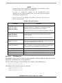
Contents
Paragraph
Number
Title
Page
Number
Chapter 1
Introduction
1.1
1.1.1
1.2
1.2.1
1.2.2
1.2.3
Overview.............................................................................................................1-1
Features ..........................................................................................................1-1
Quick Start..........................................................................................................1-3
CodeWarrior for Microcontrollers ....................................................................1-4
Install DSC56800EX_Quick_Start ..................................................................1-4
Build and Run Sample Application..................................................................1-8
Chapter 2
Core System Infrastructure
2.1
2.1.1
2.1.2
2.1.3
2.1.4
2.1.5
2.2
2.3
2.4
2.4.1
2.5
2.5.1
2.5.2
2.5.3
2.5.4
2.5.5
2.5.6
2.5.7
2.5.8
2.5.9
2.5.10
2.5.11
2.5.12
2.5.13
2.5.14
2.5.15
2.5.16
Boot Sequence ...................................................................................................2-1
Power-up/Reset...............................................................................................2-2
Start() - entry point..........................................................................................2-2
userPreMain() .................................................................................................2-3
main() the User’s Application Code.................................................................2-3
userPostMain()................................................................................................2-3
Data Types..........................................................................................................2-3
ArchIO Peripheral Register Structures ...............................................................2-4
Core System’s Routines and Macros..................................................................2-5
Architecture dependent routines .....................................................................2-5
Macros for peripheral memory access..............................................................2-11
periphMemRead - memory read ...................................................................2-11
periphMemWrite - memory write...................................................................2-11
periphBitSet - set selected bits .....................................................................2-12
periphMemInvBitSet - invert memory content and set selected bits .............2-12
periphBitClear - clear selected bits ...............................................................2-13
periphBitGrpSR - set bit group to given value...............................................2-14
periphBitGrpSRVar - set bit group to given value..........................................2-14
periphBitGrpRS - set bit group to given value...............................................2-15
periphBitGrpRSVar - set bit group to given value .........................................2-16
periphBitGrpRS32 - set bit group to given value...........................................2-16
periphBitGrpZS - set bit group to given value ...............................................2-17
periphBitGrpZSVar - set bit group to given value..........................................2-18
periphBitGrpSet - set bit group to given value ..............................................2-19
periphBitGrpSetVar - set bit group to given value .........................................2-19
periphBitGrpSet32 - set bit group to given value ..........................................2-20
periphSafeAckByOne - clear (acknowledge) bit flags which are active-high and
are cleared by write-one............................................................................2-21
DSC56800EX Quick Start User’s Guide, Rev. 2, 04/2015
Freescale Semiconductor
iii
Contents
Paragraph
Number
2.5.17
2.5.18
2.5.19
2.5.20
2.5.21
2.5.22
2.5.23
2.5.24
2.5.25
2.5.26
2.5.27
2.5.28
2.5.29
2.5.30
2.6
2.6.1
2.6.2
2.6.3
2.7
2.7.1
2.7.2
Title
Page
Number
periphSafeAckByOneVar - clear (acknowledge) bit flags which are active-high
and are cleared by write-one.....................................................................2-22
periphSafeBitClear - clear bits and keep value of bit flags which are cleared by
write-one....................................................................................................2-22
periphSafeBitSet - Set bits and keep value of bit flags which are cleared by
write-one....................................................................................................2-23
periphSafeBitSetVar - Set bits and keep value of bit flags which are cleared by
write-one....................................................................................................2-24
periphSafeBitSet32 - Set bits and keep value of bit flags which are cleared by
write-one....................................................................................................2-24
periphSafeBitGrpSet - set bit group to given value and keep value of bit flags
which are cleared by write-one..................................................................2-25
periphSafeBitGrpSetVar - set bit group to given value and keep value of bit flags
which are cleared by write-one..................................................................2-26
periphSafeBitGrpSet32 - set bit group to given value and keep value of bit flags
which are cleared by write-one..................................................................2-27
periphBitChange - change selected bits .......................................................2-28
periphBitTest - test selected bits ...................................................................2-28
periphMemDummyRead - memory dummy read..........................................2-29
periphMemForcedRead- memory force read (Never optimized out).............2-29
Miscellaneous Routines ................................................................................2-29
Intrinsic Functions .........................................................................................2-32
Interrupts ..........................................................................................................2-32
Processing Interrupts ....................................................................................2-32
Configuring Interrupts ...................................................................................2-35
Code Example ..............................................................................................2-38
Advanced Topics...............................................................................................2-45
Project Targets ..............................................................................................2-45
Inside Startup Code ......................................................................................2-46
Chapter 3
Directory Structure
3.1
3.2
3.3
3.4
3.5
3.6
Root Directory.....................................................................................................3-1
Sample Applications Directory............................................................................3-1
Tools Directory....................................................................................................3-2
Src Directory.......................................................................................................3-2
Stationery Directory ............................................................................................3-3
User_manuals Directory .....................................................................................3-3
DSC56800EX Quick Start User’s Guide, Rev. 2, 04/2015
iv
Freescale Semiconductor, Inc.
Contents
Paragraph
Number
Title
Page
Number
Chapter 4
Developing Software
4.1
4.2
4.3
4.3.1
4.3.2
4.3.3
4.4
4.5
Creating a new project........................................................................................4-1
On-chip peripheral initialization...........................................................................4-5
On-chip drivers - interface description ................................................................4-6
ioctl() ...............................................................................................................4-6
read() ..............................................................................................................4-7
write() ..............................................................................................................4-8
Interrupts and Interrupt Service Routines...........................................................4-8
appconfig.h file....................................................................................................4-8
Chapter 5 On-chip Drivers
5.1
5.1.1
5.1.2
5.1.3
5.1.4
5.1.5
5.1.6
5.1.7
5.1.8
5.1.9
5.1.10
5.1.11
5.1.12
5.1.13
5.1.14
5.1.15
5.1.16
5.1.17
5.1.18
5.1.19
5.1.20
5.1.21
5.1.22
5.1.23
5.1.24
5.1.25
5.1.26
API Specification.................................................................................................5-4
12-bit Cyclic Analog-to-Digital Converter (ADC) Driver...................................5-6
16-bit SAR Analog-to-Digital Converter (ADC16) .........................................5-23
Crossbar AND/OR/INVERT (AOI) Driver ......................................................5-30
Computer Operating Properly (COP) Driver .................................................5-35
Cyclic Redundancy Check (CRC) Driver ......................................................5-37
12-bit Digital-to-Analog Converter (DAC) Driver ...........................................5-40
DMA Controller (DMA ) Driver.......................................................................5-43
Enhanced Flexible Pulse Width Modulator (EFPWM) Driver ........................5-48
Enhanced Quadrature Encoder/Decoder (ENC)...........................................5-68
External Watchdog Monitor (EWM) Driver ....................................................5-75
FlexCAN (FCAN) Driver ................................................................................5-77
Flash Memory Module (FTFA) Driver............................................................5-84
Flash Memory Module (FTFL) Driver............................................................5-85
Flash Memory Controller (FMC) Driver.........................................................5-86
General-Purpose Input/Output (GPIO) Driver...............................................5-87
High Speed Comparator (HSCMP) Driver ....................................................5-91
Inter-Integrated Circuit (IIC) Driver................................................................5-94
Interrupt Controller (INTC) Driver................................................................5-101
Miscellaneous Control Module (MCM) Driver .............................................5-103
Modular/Scalable Controller Area Network (MSCAN) Driver ......................5-104
On-Chip Clock Synthesis (OCCS) Driver....................................................5-116
Periodic Interrupt Timer (PIT) Driver ...........................................................5-123
Power Management Controller (PMC) Driver..............................................5-125
Programmable Delay Block (PDB) ..............................................................5-127
Quad Timer (QT) Driver ..............................................................................5-135
Queued Serial Communication Interface (SCI) Driver ................................5-142
DSC56800EX Quick Start User’s Guide, Rev. 2, 04/2015
Freescale Semiconductor
v
Contents
Paragraph
Number
5.1.27
5.1.28
5.1.29
Title
Page
Number
Serial Peripheral Interface (SPI) Driver .......................................................5-148
System (SYS) Driver ...................................................................................5-152
Inter-Peripheral Crossbar Switch (XBAR) Driver ........................................5-165
Chapter 6
FreeMASTER Driver
6.1
6.2
6.3
6.4
6.4.1
6.4.2
6.5
6.6
6.6.1
6.6.2
6.6.3
Introduction .........................................................................................................6-1
Driver Files..........................................................................................................6-2
Interrupt Handling ...............................................................................................6-3
New Features......................................................................................................6-4
Target-side Addressing ...................................................................................6-4
Application Command Callbacks ....................................................................6-4
Driver Configuration............................................................................................6-4
Driver Usage.....................................................................................................6-10
Driver API......................................................................................................6-10
Code Listing: freemaster_demo....................................................................6-27
Code Listing: freemaster_demo2 ..................................................................6-32
Chapter 7
Graphical Configuration Tool
7.1
7.1.1
7.1.2
7.2
7.2.1
7.2.2
Introduction .........................................................................................................7-1
Features ..........................................................................................................7-1
How does it work?...........................................................................................7-2
Program usage ...................................................................................................7-3
GUI Description...............................................................................................7-3
Application Configuration File Structure..........................................................7-9
Chapter 8
License
8.1
Software License Agreement..............................................................................8-1
Chapter 9
Revision history
DSC56800EX Quick Start User’s Guide, Rev. 2, 04/2015
vi
Freescale Semiconductor, Inc.
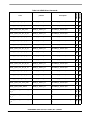
Tables
Table
Number
2-1
2-2
2-3
2-4
2-5
2-6
2-7
2-8
2-9
2-10
2-11
2-12
2-13
2-14
2-15
2-16
2-17
2-18
2-19
2-20
2-21
2-22
2-23
2-24
2-25
2-26
2-27
2-28
2-29
2-30
2-31
2-32
2-33
2-34
2-35
5-1
5-2
5-3
5-4
5-5
5-6
Title
Page
Number
Tables
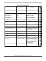
archGetSetSaturationMode arguments...................................................................2-10
archDelay arguments ..............................................................................................2-10
periphMemRead arguments....................................................................................2-11
periphMemWrite arguments....................................................................................2-11
periphBitSet arguments...........................................................................................2-12
periphMemInvBitSet arguments..............................................................................2-12
periphBitClear arguments .......................................................................................2-13
periphBitSet arguments...........................................................................................2-14
periphBitSet arguments...........................................................................................2-14
periphBitSet arguments...........................................................................................2-15
periphBitSet arguments...........................................................................................2-16
periphBitSet arguments...........................................................................................2-17
periphBitSet arguments...........................................................................................2-17
periphBitSet arguments...........................................................................................2-18
periphBitSet arguments...........................................................................................2-19
periphBitSet arguments...........................................................................................2-19
periphBitSet arguments...........................................................................................2-20
periphSafeAckByOne arguments ............................................................................2-21
periphSafeAckByOneVar arguments.......................................................................2-22
periphSafeBitClear arguments ................................................................................2-22
periphSafeBitSet arguments ...................................................................................2-23
periphSafeBitSetVar arguments ..............................................................................2-24
periphSafeBitSet arguments ...................................................................................2-24
periphSafeBitGrpSet arguments .............................................................................2-25
periphSafeBitGrpSetVar arguments........................................................................2-26
periphSafeBitGrpSet arguments .............................................................................2-27
periphBitChange arguments ...................................................................................2-28
periphBitTest arguments .........................................................................................2-28
periphMemDummyRead arguments .......................................................................2-29
periphMemForcedRead arguments ........................................................................2-29
impyuu arguments...................................................................................................2-30
impysu arguments ...................................................................................................2-30
shl2 arguments........................................................................................................2-31
shr2 arguments .......................................................................................................2-31
Targets of the MC56F82748EVM project. ...............................................................2-45
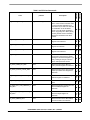
Driver Arguments - ioctl.............................................................................................5-4
Identifiers for ADC Driver ..........................................................................................5-6
ADC Driver Commands.............................................................................................5-6
Identifiers for ADC16 Driver ....................................................................................5-23
ADC16 Driver Command ........................................................................................5-23
Identifiers for AOI Driver ..........................................................................................5-30
DSC56800EX Quick Start User’s Guide, Rev. 2, 04/2015
Freescale Semiconductor
vii
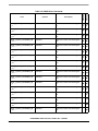
Tables
Table
Number
5-7
5-8
5-9
5-10
5-11
5-12
5-13
5-14
5-15
5-16
5-17
5-18
5-19
5-20
5-21
5-22
5-23
5-24
5-25
5-26
5-27
5-28
5-29
5-30
5-31
5-32
5-33
5-34
5-35
5-36
5-37
5-38
5-39
5-40
5-41
5-42
5-43
5-44
5-45
5-46
5-47
Title
Page
Number
AOI Driver Commands ............................................................................................5-30
Identifiers for COP Driver ........................................................................................5-35
COP Driver Commands ..........................................................................................5-35
Identifiers for CRC Driver ........................................................................................5-37
CRC Driver Commands ..........................................................................................5-37
Identifiers for DAC Driver.........................................................................................5-40
DAC Driver Commands ...........................................................................................5-40
Identifiers for DMA Driver .......................................................................................5-43
DMA Driver Commands ..........................................................................................5-43
Identifiers for DMA Driver ........................................................................................5-44
DAC_x Driver Commands .......................................................................................5-44
Identifiers for EFPWM Driver...................................................................................5-48
EFPWM Driver Commands.....................................................................................5-48
Identifiers for ENC Driver ........................................................................................5-68
ENC Driver Command ............................................................................................5-68
Identifiers for EWM Driver .......................................................................................5-75
EWM Driver Commands .........................................................................................5-75
Identifiers for FCAN Driver ......................................................................................5-77
FCAN Driver Command ..........................................................................................5-77
FCAN driver - MB-specific commands ....................................................................5-82
Identifiers for FTFA Driver .......................................................................................5-84
FTFA Driver Command ...........................................................................................5-84
Identifiers for FTFL Driver .......................................................................................5-85
FTFL Driver Command ...........................................................................................5-85
Identifiers for FMC Driver ........................................................................................5-86
FMC Driver Command ............................................................................................5-86
Identifiers for GPIO Driver .......................................................................................5-87
GPIO Driver Commands .........................................................................................5-87
Identifiers for HSCMP Driver ...................................................................................5-91
HSCMP Driver Commands .....................................................................................5-91
Identifiers for I2C Driver ..........................................................................................5-94
IIC Driver Commands..............................................................................................5-94
Identifiers for INTC Driver......................................................................................5-101
INTC Driver Commands ........................................................................................5-101
Identifiers for MCM Driver .....................................................................................5-103
MCM Driver Command .........................................................................................5-103
Identifiers for MSCAN Driver .................................................................................5-104
MSCAN Driver Commands ...................................................................................5-104
Identifiers for MSCAN Driver .................................................................................5-113
MSCANMB Driver Commands..............................................................................5-113
Identifiers for OCCS Driver....................................................................................5-116
DSC56800EX Quick Start User’s Guide, Rev. 2, 04/2015
viii
Freescale Semiconductor
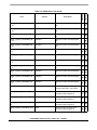
Tables
Table
Number
5-48
5-49
5-50
5-51
5-52
5-53
5-54
5-55
5-56
5-57
5-58
5-59
5-60
5-61
5-62
5-63
5-64
6-1
6-2
6-3
9-1
Title
Page
Number
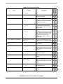
OCCS Driver Commands ......................................................................................5-116
Identifiers for PIT Driver ........................................................................................5-123
PIT Driver Commands...........................................................................................5-123
Identifiers for PMC Driver ......................................................................................5-125
PMC Driver Commands ........................................................................................5-125
Identifiers for PDB Driver.......................................................................................5-127
PDB Driver Command...........................................................................................5-127
Identifiers for QTIMER Driver ................................................................................5-135
QT Driver Commands ...........................................................................................5-136
Identifiers for SCI Driver ........................................................................................5-142
SCI Driver Commands ..........................................................................................5-142
Identifiers for SPI Driver ........................................................................................5-148
SPI Driver Commands ..........................................................................................5-148
Identifiers for SYS Driver.......................................................................................5-152
SYS Driver Commands .........................................................................................5-152
Identifiers for XBAR Driver ....................................................................................5-165
XBAR Driver Commands ......................................................................................5-165
FreeMASTER Driver Interrupt Mode .........................................................................6-3
FreeMASTER Communication Configuration Items for appconfig.h .........................6-5
TSA Type Constants ...............................................................................................6-25
Revision history.........................................................................................................9-1
DSC56800EX Quick Start User’s Guide, Rev. 2, 04/2015
Freescale Semiconductor
ix
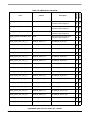
Figures
Figure
Number
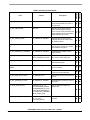
1-1
1-2
1-3
1-4
1-5
1-6
1-7
1-8
2-1
2-2
2-3
3-1
3-2
3-3
3-4
4-1
4-2
4-3
4-4
4-5
5-1
6-1
7-1
7-2
7-3
7-4
7-5
7-6
7-7
7-8
Title
Page
Number
Figures
Software Structure ....................................................................................................1-2
External Tool Configurations .....................................................................................1-5
GCT Integration.........................................................................................................1-6
Build Before Launch ..................................................................................................1-6
GCT Key Binding.......................................................................................................1-7
Import Dialog Box......................................................................................................1-9
Root Directory Selection ...........................................................................................1-9
Drag & Drop CodeWarrior Project File ....................................................................1-10
Boot Sequence..........................................................................................................2-1
Interrupt Processing Flow .......................................................................................2-34
Memory Checking Process .....................................................................................2-53
Root Directory Structure ...........................................................................................3-1
Sample Applications Directory Structure ..................................................................3-2
Src Directory Structure..............................................................................................3-3
Stationery Directory Structure...................................................................................3-3
Import Dialog Box......................................................................................................4-1
Project Import Settings..............................................................................................4-2
Drag & Drop CodeWarrior Project File ......................................................................4-3
DSC56800EX_Quick_Start Variable .........................................................................4-4
User Interface............................................................................................................4-6
Macro Expansion Process ........................................................................................5-3
FreeMASTER Application Window............................................................................6-2
GCT Usage ...............................................................................................................7-2
GCT Main Window ....................................................................................................7-4
Pinout Page Status Icons ..........................................................................................7-5
Pinout Page...............................................................................................................7-6
Register View ............................................................................................................7-7
Warnings View ..........................................................................................................7-8
Options dialog ...........................................................................................................7-9
The appconfig.h File................................................................................................7-10
DSC56800EX Quick Start User’s Guide, Rev. 2, 04/2015
x
Freescale Semiconductor
Chapter 1
Introduction
This user’s manual is targeted for Freescale 56F82xxx and 56F84xxx application developers. Its purpose
is to describe the development environment, the software modules and the tools for the 56F82xxx and
56F84xxx and the Application Programming Interface (API). Simply, this manual describes how to use
the Freescale DSC56800EX_Quick_Start tool to develop software for the Freescale 56F82xxx and
56F84xxx Digital Signal Controllers (DSC).
1.1
Overview
The DSC56800EX_Quick_Start development environment provides fully debugged peripheral drivers,
examples and interfaces, that allow programmers to create their own C application code, independent of
the core architecture. This environment has been developed to complement the existing development
environment for Freescale 56F8xxx embedded processors. It provides a software infrastructure that allows
development of efficient, ready to use high level software applications, that are fully portable and reusable
between different core architectures. The maximum portability is achieved for devices with comparable
on-chip peripheral modules.
This manual contains information specific only to DSC56800EX_Quick_Start tool as it applies to the
Freescale 56F8xxx software development. Therefore it is required that users of the
DSC56800EX_Quick_Start tool should be familiar with the 56800E family in general, as described in the
DSP56800E and DSP56800EX 16-Bit DSP Core Reference Manual (DSP56800ERM/D),
MC56F84XXX Reference Manual (MC56F84XXXRM) and the 56F82XXX Reference Manual
(MC56F82XXXRM), before continuing. The 56F82xxx and 56F84xxx devices are supported by a
complete set of hardware development boards - Tower modules (TWRs).
Comprehensive information about available tools and documentation can be found on Freescale web
pages:
freescale.com
Freescale DSC56800EX_Quick_Start tool is designed for and can be fully integrated with Freescale
CodeWarrior development tools. Before starting to explore the full feature set of the
DSC56800EX_Quick_Start, one should install and become familiar with the CodeWarrior development
environment.
All together, the DSC56800EX_Quick_Start, the CodeWarrior, and the TWRs create a complete and
scalable tool solution for easy, fast and efficient development.
1.1.1
Features
The DSC56800EX_Quick_Start environment is composed of the following major components:
core-system infrastructure, on-chip drivers with defined API, sample example applications, Graphical
Configuration Tool and FreeMASTER software support. This section brings very illustrative information
about these components, while the comprehensive description can be found in specially targeted chapters.
DSC56800EX Quick Start User’s Guide, Rev. 2, 04/2015
Freescale Semiconductor, Inc.
1-1
1.1.1.1
Core-system Infrastructure
The core-system infrastructure creates the fundamental infrastructure for the 56F82xxx and 56F84xxx
device operation and enables further integration with other components, e.g. on-chip drivers. The basic
development support provided includes: setting of the required operation mode, commonly used macro
definitions, portable architecture-dependent register declaration, mechanism for static configuration of
on-chip peripherals as well as interrupt vectors, and the project templates.
1.1.1.2
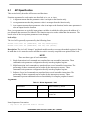
On-chip Drivers
The on-chip drivers isolate the hardware-specific functionality into a set of driver commands with defined
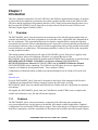
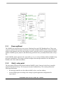
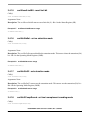
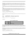
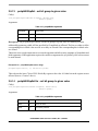
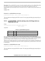
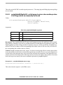
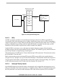
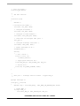
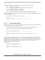
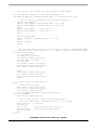
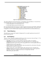
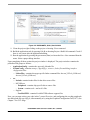
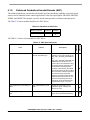
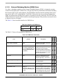
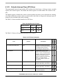
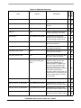
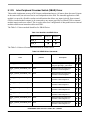
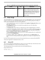
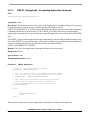
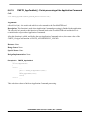
API. The API standardizes the interface between the software and the hardware, see Figure 1-1. This
isolation enables a high degree of portability or architectural and hardware independence for application
code. This is mainly valid for devices with similar peripheral modules. The driver code reuses lead for
greater efficiency and performance.
APPLICATION
API
ON-CHIP DRIVERS
HARDWARE
on-chip peripheral modules
Figure 1-1. Software Structure
1.1.1.3
Sample Applications
The DSC56800EX_Quick_Start tool contains many sample applications that demonstrate how to use
on-chip drivers and how to implement some user-specific tasks. These sample examples are kept simple
and illustrative and their intention is to minimize the learning curve.
1.1.1.4
Graphical Configuration Tool
The Graphical Configuration Tool (GCT) is a graphical user interface (GUI), designed to provide static
chip and on-chip peripheral module setting/initialization, including association of the interrupt vectors
with user interrupt service routines.
The Graphical Configuration Tool is not required in order to use the DSC56800EX_Quick_Start
environment, i.e. it is optional. Nevertheless, this tool simplifies the configuration of on-chip peripheral
DSC56800EX Quick Start User’s Guide, Rev. 2, 04/2015
1-2
Freescale Semiconductor, Inc.
modules and the device itself. It also guides the user by supplying a lot of useful information and hints. It
is therefore recommended to use the Graphical Configuration Tool.
1.1.1.5
FreeMASTER Software
The FreeMASTER application is a software tool initially created for developers of Motor Control
applications, but it may be extended to any other application development. This tool allows remote control
of an application using a user-friendly graphical environment running on a PC. It also provides the ability
to view some real-time application variables in both textual and graphical form.
Main features:
• Graphical environment
• Visual Basic Script or Java Script can be used for control of target board
• Easy to understand navigation
• Connection to target board possible over a network, including Internet
• Demo mode with password protection support
• Visualization of real-time data in Scope window
• Acquisition of fast data changes using integrated Recorder
• Value interpretation using custom defined text messages
• Built-in support for standard variable types (integer, floating point, bit fields)
• Several built-in transformations for real type variables
• Automatic variable extraction from CodeWarrior linker output files (MAP, ELF)
• Remote control of application execution
The FreeMASTER tool is not required in order to use the DSC56800EX_Quick_Start environment, i.e. it
is optional. Nevertheless, FreeMASTER is a versatile tool to be used for multipurpose algorithms and
applications. It provides a lot of excellent features, including:
• Real-Time debugging
• Diagnostic tool
• Demonstration tool
• Education tool
The full description can be found in the FreeMASTER User Manual attached to the FreeMASTER tool.
1.2
Quick Start
This chapter provides the information required to get the DSC56800EX_Quick_Start tool installed and
running.
DSC56800EX Quick Start User’s Guide, Rev. 2, 04/2015
Freescale Semiconductor, Inc.
1-3
1.2.1
CodeWarrior for Microcontrollers
CodeWarrior Development Studio V10.3 (or later) is a complete Integrated Development Environment
(IDE) that provides a highly visual and automated framework to accelerate development of the most
complex embedded applications.
CodeWarrior for Microcontrollers integrates the development tools for the ColdFire®, ColdFire+, DSC,
Kinetis, Qorivva, PX, RS08, S08, and S12Z architectures into a single product based on the Eclipse open
development platform. Eclipse offers an excellent framework for building software development
environments and is a standard framework used by many embedded software vendors.
As previously mentioned, DSC56800EX_Quick_Start tool is designed for and can be integrated with
CodeWarrior for Microcontrollers development tool. With CodeWarrior for Microcontrollers tool, users
can build applications and integrate other software included as part of the DSC56800EX_Quick_Start
release. Once the software is built, CodeWarrior tools allows users to download executable images into the
target platform and run or debug the downloaded code.
To install CodeWarrior for Microcontrollers V10.3, it is recommended to use the installation guide
attached to the actual version of CodeWarrior for Microcontrollers, if available.
1.2.2
Install DSC56800EX_Quick_Start
In order for the DSC56800EX_Quick_Start to integrate itself with the development tools, the CodeWarrior
tools should be installed prior to the installation of DSC56800EX_Quick_Start installation (see previous
section). If the DSC56800EX_Quick_Start tool is installed while CodeWarrior is not present, users can
only browse the installed software package, but will not be able to build, download and run the released
code. However, the installation can be simply completed once CodeWarrior is installed, see Section 1.2.1.
The installation itself consists of copying the required files to the destination hard drive, checking the
presence of CodeWarrior and creating the shortcut under the Start->Programs menu. It is recommended to
use the default installation directory path c:\Freescale\... .
NOTE
Each DSC56800EX_Quick_Start release is installed in its own new
directory named DSC56800EX_Quick_Start rX.Y (where X.Y denotes the
release number). Thus, it enables to maintain the older releases and projects.
It gives free choice to select the active release.
To start the installation process, perform the following steps:
1. Execute DSC56800EX_Quick_Start_rXY.exe
2. Follow the DSC56800EX_Quick_Start software installation instructions on your screen.
3. In case the installation directory is different than default path, it is essential to change
DSC56800EX_Quick_Start path variable in CodeWarrior Development Studio
DSC56800EX Quick Start User’s Guide, Rev. 2, 04/2015
1-4
Freescale Semiconductor, Inc.
1.2.2.1
Install Graphical Configuration Tool
Graphical Configuration Tool is installed together with the DSC56800EX_Quick_Start environment as
part of the Typical installation. Graphical configuration tool can also be installed as a selectable component
within the Custom installation.
Graphical Configuration Tool is able to work as stand-alone, but integration with the CodeWarrior IDE
markedly increases the efficiency of this tool. The integration is based on the IDE user-configurable menus
and its interface for external plug-ins.
NOTE
External Tool Configurations are set only for the actual Workspace. Newly created
Workspace requires new configuration setting for GCT integration.
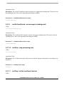
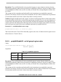
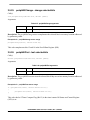
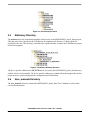
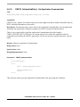
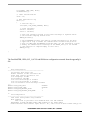
To integrate the Graphical Configuration Tool with CodeWarrior Workspace, perform the following steps:
a) Launch CodeWarrior IDE from the Start->Programs->Freescale CodeWarrior menu.
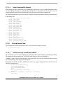
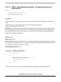
b) Open the External Tools Configurations dialog window using Run->External Tools->External
Tools Configurations.
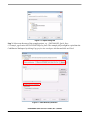
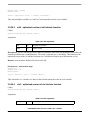
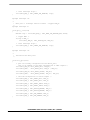
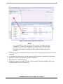
Figure 1-2. External Tool Configurations
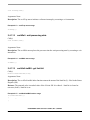
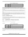
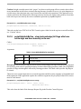
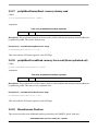
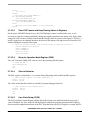
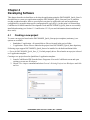
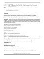
c) Set the GCT launcher settings in Main tab Location (path to the project folder should be less
than 120 characters and must not contain a "space" character), Working directory and
Arguments as a system variable ${project_loc}.
DSC56800EX Quick Start User’s Guide, Rev. 2, 04/2015
Freescale Semiconductor, Inc.
1-5
Figure 1-3. GCT Integration
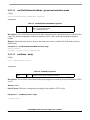
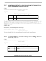
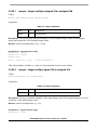
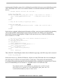
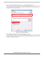
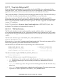
d) Untick the Build before lanunch box and click Apply.
Figure 1-4. Build Before Launch
e)
f)
g)
h)
i)
Click on Run button.
Optionally the key bidding for GCT might be set.
Open Window -> Preferences dialog box.
Search for “keys” and “run last” in Preferences window.
Select “Run Last Launched External Tool” in command menu.
DSC56800EX Quick Start User’s Guide, Rev. 2, 04/2015
1-6
Freescale Semiconductor, Inc.
j) Set required binding.
Figure 1-5. GCT Key Binding
k) Click on “Apply” and “OK” buttons.
Now you should be able to execute the Graphical Configuration Tool from the CodeWarrior IDE menu
Run->External Tools->GCT by clicking on the icon or by pressing the chosen key shortcut. Note that the
DSC56800EX_Quick_Start project should be open in the Workspace to quickly execute the Graphical
Configuration Tool.
1.2.2.2
1.2.2.2.1
Install FreeMASTER (PC Master Software)
System Requirements
The FreeMASTER application can run on any computer with Microsoft Windows 98 or later operating
system. Before installing, the Internet Explorer 4.5.5 or higher.
Operating system: Microsoft Windows XP, Windows 2000, Windows NT4 with SP6, Windows 98,
through Window 7 (on the host side)
Required software: Internet Explorer 4.5.5 or higher installed. For selected features (e.g. regular
expression-based parsing), Internet Explorer 5.5 or higher is required.
Hard drive space: 108 MB
DSC56800EX Quick Start User’s Guide, Rev. 2, 04/2015
Freescale Semiconductor, Inc.
1-7
Other hardware requirements: Mouse, serial RS-232 port for local control, network access for remote
control
1.2.2.2.2
Target Development Board Requirements
To enable the FreeMASTER connection to the target board application, follow the instructions provided
with the embedded-side development tool. The recommended and fastest way to start using FreeMASTER
is by trying the sample application.
FreeMASTER software relies on the following items to be provided by the target development board:
Interface: Serial communication port or the JTAG port (available on all Freescale EVM boards).
Data RAM Memory: Approximately 160 words of data memory plus the size of the recorder buffer is
needed for the full configuration. Optionally, some features can be disabled to reduce required data
memory size.
Program Flash Memory: Required size is approximately 2K words for the full configuration. Optionally,
some features can be removed to reduce required program memory size
1.2.2.2.3
Enabling FreeMASTER on Target Application
To enable the FreeMASTER operation on the target board application, see description and an example in
Chapter 6, “FreeMASTER Driver.”
1.2.2.2.4
How to Install
The FreeMASTER application is an optional part of the DSC56800EX_Quick_Start environment and
must be installed separately, e.g. running the FMASTERSW_v16.exe (or later).
1.2.3
Build and Run Sample Application
Once the DSC56800EX_Quick_Start tool is installed, the user can build and run any released demo
application for the TWR DSC modules by opening and building the project and using the CodeWarrior
development environment. pwm_demo is used as an example in this case.
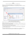
Two methods can be used to open an example project Import (Step 2&3) or drag&drop (Step 4):
Step 1: Launch CodeWarrior IDE from the Start->Programs->Freescale CodeWarrior menu and open
existing or create new Workspace.
Step 2: Choose File->Import command and select General->Existing Projects into Workspace and click
on Next.
DSC56800EX Quick Start User’s Guide, Rev. 2, 04/2015
1-8
Freescale Semiconductor, Inc.
Figure 1-6. Import Dialog Box
Step 3: Select root directory of the example project, e.g ..\DSC56800EX_Quick_Start
r2.6\sample_applications\MC56F8200TWR\pwm_demo. The example project might be copied into the
CodeWarrior Workspace by ticking Copy project into workspace tick box and click on Finish.
Figure 1-7. Root Directory Selection
DSC56800EX Quick Start User’s Guide, Rev. 2, 04/2015
Freescale Semiconductor, Inc.
1-9
NOTE
Select the corresponding directory according to your TWR DSC board
Step 4: Select root directory of the example project, e.g. ..\DSC56800EX_Quick_Start
r2.6\sample_applications\MC56F8200TWR\pwm_demo. Drag and drop .project file to the CodeWarrior
Workspace Project Tab.
Figure 1-8. Drag & Drop CodeWarrior Project File
Step 5: Clean the project right clicking on the project a choosing Clean command.
Step 6: Build the application code by pressing Ctrl+B or choosing Project->Build All command. Check if
there is zero errors after the application building.
Step 7:Run the application by pressing the green arrow (Run) or choose the Run->Run command from the
menu. Select proper debug interface for SDM configuration.
At this point, the application is running - the LEDs associated to the PWM outputs are flashing and the
green LED is blinking periodically.
The subsequent chapters describe how to create a new application, how to use interrupts, how to use
on-chip drivers, and other information required to successfully create a new application.
DSC56800EX Quick Start User’s Guide, Rev. 2, 04/2015
1-10
Freescale Semiconductor, Inc.
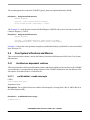
Chapter 2
Core System Infrastructure
The Core System Infrastructure is one of the three main blocks that compose the 56800EX_Quick_Start
tool (see Section 1.1.1 where the partitioning is described). Its purpose is to provide the fundamental
infrastructure for the 56800EX device operation (e.g. sets the operation mode, the interrupt handling, the
initialization of the global variables, CodeWarrior Compiler options). It also provides some additional
support (commonly used macros, data types) and enables further integration with On-chip Drivers.
2.1
Boot Sequence
The Core System Infrastructure provides the fundamental code which is executed before the user’s main
function. This code provides basic settings needed to initialize the chip, settings required by the
CodeWarrior Compiler, initialization of global variables. Finally it passes control to the user’s application
code (the main function).
NOTE
This chapter describes the boot process of the 56F82xxx and 56F84xxx
family of microcontrollers.
For the 56F82xxx and 56F84xxx devices, the post-reset execution flow may be briefly described as
follows (also see Figure 2-1):
1. After processor reset, the execution starts at the Hardware Reset vector in program memory, where
the 56800EX_Quick_Start tool places its jump to the Start() assembly routine. The reset vector is
located at address 0x0000 and the jump is supplied directly from the first entry of vector table
located in the interrupt_vectors section in vectors.c file.
2. If the chip reset is generated by the watchdog module (COP), the same rules as in the previous point
apply. Again the COP Reset vector is supplied from the full vector table at address 0x0000
(interrupt_vectors section). The default value of COP Reset vector is Start(), so the standard
power-up code is processed. The user is able to redefine the COP Reset service routine same way
the other interrupt vectors are installed (see Section 2.6.2 on page -35 for more details).
3. Start() assembly routine (in startup.c file)
4. userPreMain() function (in appconfig.c file)
5. user’s main() function (in default project it is located in main.c)
6. userPostMain() function (in appconfig.c file)
The following subsections provide a detailed description of all initialization performed before user’s
main() function is called.
Figure 2-1. Boot Sequence
DSC56800EX Quick Start User’s Guide, Rev. 2, 04/2015
Freescale Semiconductor, Inc.
2-1
2.1.1
Power-up/Reset
The 56800EX core specifies two reset vectors: Hardware Reset and COP Watchdog Reset. These reset
vectors are located at the locations of interrupt vector table at address 0x0000. These vectors identify the
address of the program code where the program control is passed to on reset. In applications developed
with the 56800EX_Quick_Start tool, the default entry point is the Start() assembly routine in the startup.c
file.
In the 56800EX_Quick_Start tool, the vector table (vectors.c) is always linked at address 0x0000 for any
processor configuration. The startup code then configures the interrupt controller to use the address
0x0000 as the vector table base address.
2.1.2
Start() - entry point
The entry point of all projects developed with the 56800EX_Quick_Start tool is the Start() assembly
routine located in the startup.c file in {project}\SystemConfig directory. This routine performs the
following initialization:
• the interrupt controller uses the address 0x0000 as the vector base address
• sets the OMR register according to the settings in global application configuration file
(appconfig.h)
DSC56800EX Quick Start User’s Guide, Rev. 2, 04/2015
2-2
Freescale Semiconductor, Inc.
•
•
•
•
•
•
•
initializes the On-chip Clock Synthesis (OCCS) module, sets the PLL (by values from appconfig.h)
and waits while the generated clock is stable
initializes the stack pointer (SP) to the address after any data segments
clears the .bss segment which holds the uninitialized global and static C variables
copies the initial values from Flash memory to initialized global C variables (.data segment). The
P-Flash memory is used to hold the initialization data.
clears and initializes variables in the fardata.bss and fardata.data segments
clears and initializes variables in the .bss.pmem and .bss.data segment (program RAM-based
variables)
initializes the program RAM-based code of the pramcode section.
When all the initialization is done, the functions userPreMain(), main(), userPostMain() are called.
2.1.3
userPreMain()
The userPreMain() function is called before the main application code in the main() function. The user can
add any additional initialization code here. The function is located in the appconfig.c file.
2.1.4
main() the User’s Application Code
The main() function is called after all the code described above is executed (i.e. the processor is initialized
and the user’s pre-main code is executed). It is the place where the user writes the application code. By
default the function is located in the main.c file, but the file can be renamed by the user.
2.1.5
userPostMain()
The userPostMain() function is called after the main application code is finished. The user can add any
additional code he/she wishes. By default the processor is halted by debughlt instruction here. The function
is located in the appconfig.c file.
2.2
Data Types
The 56800EX_Quick_Start tool defines some basic data types to support code portability between
different hardware architectures and tools. These basic data types, which are defined in the C header file
types.h, support International Telecommunication Union (ITU) generic word types, integer, fractional, and
complex data types. This is used throughout the interface definitions for the On-Chip Drivers. Note that in
some development environments these data type definitions are located in the prototype.h file.
1. Generic word types
• Word8 - to represent 8-bit signed character variable/value
• UWord8 - to represent 16-bit unsigned character variable/value
• Word16 - to represent 16-bit signed variable/value
• UWord16 - to represent 16-bit unsigned variable/value
• Word32 - to represent 32-bit signed variable/value
DSC56800EX Quick Start User’s Guide, Rev. 2, 04/2015
Freescale Semiconductor, Inc.
2-3
•
2.
•
•
•
•
•
•
3.
•
•
•
•
4.
•
5.
•
•
•
•
•
•
•
•
•
2.3
UWord32 - to represent 32-bit unsigned variable/value
Integer types
Int8 - to represent 8-bit signed character variable/value
UInt8 - to represent 8-bit unsigned character variable/value
Int16 - to represent 16-bit signed variable/value
UInt16 - to represent 16-bit unsigned variable/value
Int32 - to represent 32-bit signed variable/value
UInt32 - to represent 32-bit unsigned variable/value
Fractional types
Frac16 - to represent 16-bit signed variable/value
Frac32 - to represent 32-bit signed variable/value
CFrac16 - to represent 16-bit complex numbers
CFrac32 - to represent 32-bit complex numbers
Miscellaneous types
bool - to represent boolean variable (true/false)
Constants
true - represents true value
false - represents false value
NULL - represents null pointer
PASS - represents pass as function result
FAIL - represents fail as function result
MAX_32 - maximum 32-bit signed (Word32) value
MIN_32 - minimum 32-bit signed (Word32) value
MAX_16 - maximum 16-bit signed (Word16) value
MIN_16 - minimum 16-bit signed (Word16) value
ArchIO Peripheral Register Structures
The global symbol ArchIO provides a C interface (structure type) to all peripheral and core registers
mapped in data memory. All registers are accessed via this structure so there is no need to know and specify
the concrete addresses of the registers to write or read. This mechanism increases code readability and
portability and simplifies access to registers. The ArchIO is declared in the C header file arch.h.
The ArchIO is of type arch_sIO, which is the structure type composed from another structures, one for each
peripheral module.
There are two possible approaches how to define and use the ArchIO structure:
• define ArchIO as the direct (numeric) address of memory-mapped peripheral registers casted to the
proper structure type.
• define ArchIO as the extern variable while defining its address by a directive in linker command
file.
DSC56800EX Quick Start User’s Guide, Rev. 2, 04/2015
2-4
Freescale Semiconductor, Inc.
The second approach is used in the 56800EX_Quick_Start tool implementation by default.
Example 2-1. Using the ArchIO structure
UWord16 RegValue;
RegValue = ArchIO.TimerD.Channel0.HoldReg;
ArchIO.TimerD.Channel0.CompareReg1 = 0x8000;
The Example 2-1 reads the timer/counter D0 Hold Register (HOLD) and writes to the timer/counter D0
Compare Register 1 (CMP1).
Example 2-2. Using the ArchIO structure
UWord16 RegValue;
RegValue = periphMemRead(&ArchIO.TimerD.Channel0.HoldReg);
periphMemWrite(0x8000, &ArchIO.TimerD.Channel0.CompareReg1);
Example 2-2 shows the same operation using the periphMemRead and periphMemWrite macros described
later in Section 2.5:
2.4
Core System’s Routines and Macros
This section describes routines, macros and intrinsic function redefinition provided by the Core System
Infrastructure.
2.4.1
Architecture dependent routines
This section describes architecture dependent routines and macros which provide interface to the 56800EX
core architecture. It encapsulates the unique features of the 56800EX architecture into the abstract APIs.
All routines are defined in the arch.h header file.
2.4.1.1
archEnableInt - enable interrupts
Call(s):
void archEnableInt(void);
Arguments: None.
Description: The archEnableInt macro enables all interrupts by clearing bits I1 (Bit 9) and I0 (Bit 8) in
the Status Register (SR).
Example 2-3. archEnableInt macro usage
archEnableInt();
DSC56800EX Quick Start User’s Guide, Rev. 2, 04/2015
Freescale Semiconductor, Inc.
2-5
2.4.1.2
archEnableIntLvl123 - enable interrupt levels 1, 2 and 3
Call(s):
void archEnableIntLvl123(void);
Arguments: None.
Description: The archEnableIntLvl123 macro enables interrupts at levels 1, 2 and 3 while masking the
interrupts at level 0. It is accomplished by clearing bit I1 (Bit 9) and setting bit I0 (Bit 8) in the Status
Register (SR).
Example 2-4. archEnableIntLvl123 macro usage
archEnableIntLvl123();
2.4.1.3
archEnableIntLvl23 - enable interrupts levels 2 and 3
Call(s):
void archEnableIntLvl23(void);
Arguments: None.
Description: The archEnableIntLvl23 macro enables interrupts at levels 2 and 3 while masking interrupts
at levels 0 and 1. It is accomplished by setting bit I1 (Bit 9) and clearing I0 (Bit 8) in the Status Register
(SR).
Example 2-5. archEnableIntLvl23 macro usage
archEnableIntLvl23();
2.4.1.4
archDisableInt - disable interrupts
Call(s):
void archDisableInt(void);
Arguments: None.
Description: The archDisableInt macro disables all maskable interrupts by setting bits I1 and I0 (Bits 9 8) in the Status Register (SR).
Example 2-6. archDisableInt macro usage
archDisableInt();
DSC56800EX Quick Start User’s Guide, Rev. 2, 04/2015
2-6
Freescale Semiconductor, Inc.
2.4.1.5
archResetLimitBit - reset limit bit
Call(s):
void archResetLimitBit(void);
Arguments: None.
Description: The archResetLimitBit macro resets limit bit (L) - Bit 6 in the Status Register (SR).
Example 2-7. archResetLimitBit macro usage
archResetLimitBit();
2.4.1.6
archSetNoSat - set no saturation mode
Call(s):
void archSetNoSat(void);
Arguments: None.
Description: The archSetNoSat macro disables the saturation mode. This macro clears the saturation (SA)
bit - Bit 4 in the Operating Mode Register (OMR).
Example 2-8. archSetNoSat macro usage
archResetLimitBit();
2.4.1.7
archSetSat32 - set saturation mode
Call(s):
void archSetSat32(void);
Arguments: None.
Description: The archSetSat32 macro sets the saturation mode. This macro sets the saturation (SA) bit Bit 4 in the Operating Mode Register (OMR).
Example 2-9. archSetSat32 macro usage
archSetSat32();
2.4.1.8
archSet2CompRound - set two’s complement rounding mode
Call(s):
void archSet2CompRound(void);
DSC56800EX Quick Start User’s Guide, Rev. 2, 04/2015
Freescale Semiconductor, Inc.
2-7
Arguments: None.
Description: The archSet2CompRound macro sets the two’s complement rounding mode. This macro sets
the rounding (R) bit - Bit 5 in the Operating Mode Register (OMR).
Example 2-10. archSet2CompRound macro usage
archSet2CompRound();
2.4.1.9
archSetConvRound - set convergent rounding mode
Call(s):
void archSetConvRound(void);
Arguments: None.
Description: The archSetConvRound macro sets the convergent rounding mode. This macro clears the
rounding (R) bit - Bit 5 in the Operating Mode Register (OMR).
Example 2-11. archSetConvRound macro usage
archSetConvRound();
2.4.1.10
archStop - stop processing state
Call(s):
void archStop(void);
Arguments: None.
Description: The archStop macro places the processor into the stop processing state by executing a stop
instruction.
Example 2-12. archStop macro usage
archStop();
2.4.1.11
archTrap - initiate a software interrupt
Call(s):
DSC56800EX Quick Start User’s Guide, Rev. 2, 04/2015
2-8
Freescale Semiconductor, Inc.
void archTrap(void);
Arguments: None.
Description: The archTrap macro initiates a software interrupt by executing a swi instruction.
Example 2-13. archTrap macro usage
archTrap();
2.4.1.12
archWait - wait processing state
Call(s):
void archWait(void);
Arguments: None.
Description: The archWait macro places the processor into the wait processing state by executing a wait
instruction.
Example 2-14. archWait macro usage
archWait();
2.4.1.13
archGetLimitBit - get limit bit
Call(s):
Word16 archGetLimitBit(void);
Arguments: None.
Description: The archGetLimitBit inline function returns the status of the limit bit (L) - Bit 6 in the Status
Register (SR).
Returns: The returned value is masked value of the L-bit in SR. It is either 0 - limit bit is cleared or
non-zero (0x40) - limit bit is set.
Example 2-15. archGetLimitBit function usage
if(archGetLimitBit())
{
...
}
DSC56800EX Quick Start User’s Guide, Rev. 2, 04/2015
Freescale Semiconductor, Inc.
2-9
2.4.1.14
archGetSetSaturationMode - get and set saturation mode
Call(s):
Word16 archGetSetSaturationMode(bool bSatMode);
Arguments:
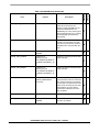
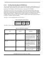
Table 2-1. archGetSetSaturationMode arguments
bSatMode
in
State of the saturation mode to be set.
false - set no saturation mode
true - set saturation mode
Description: The archGetSetSaturationMode inline function sets the saturation mode to a user specified
value. The function manipulates with the saturation (SA) bit - Bit 4 in the Operating Mode Register
(OMR).
Returns: Saturation mode prior to the new state (the return value is masked SA-bit from the previous
OMR value).
Example 2-16. archGetSetSaturationMode function usage
Word16 bSatMode;
bSatMode = archGetSetSaturationMode(true);
2.4.1.15
archDelay - delay
Call(s):
void archDelay(UWord16 Ticks);
Arguments:
Table 2-2. archDelay arguments
Ticks
in
Number of CPU cycles to delay (0 to 0xFFFF)
Description: The archDelay inline function delays the program execution by the specified number of CPU
cycles.
Returns: None.
Special Issues: The delay corresponds just roughly to the number of CPU cycles.
Example 2-17. archDelay function usage
archDelay(1000);
DSC56800EX Quick Start User’s Guide, Rev. 2, 04/2015
2-10
Freescale Semiconductor, Inc.
2.5
Macros for peripheral memory access
This section describes macros for peripheral memory access. The macros are used to read, write, set, clear,
change the memory mapped on-chip peripherals. Using these macros offers a greater portability than
simply referencing on-chip peripherals with direct memory accesses. All macros are defined in the
periph.h header file.
Required Header File(s):
#include “types.h“
#include “periph.h“
2.5.1
periphMemRead - memory read
Call(s):
UWord16 periphMemRead(UWord16 *pAddr);
Arguments:
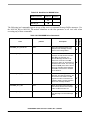
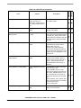
Table 2-3. periphMemRead arguments
pAddr
in
The memory address from which to read a 16-bit word.
Description: The periphMemRead macro reads a 16-bit word from the memory location addressed by
parameter pAddr.
Example 2-18. periphMemRead macro usage
UWord16 RegValue;
RegValue = periphMemRead(&ArchIO.TimerD.ch0.hold);
This code reads the content of the timer/counter D0 Hold Register (HOLD).
2.5.2
periphMemWrite - memory write
Call(s):
UWord16 periphMemWrite(UWord16 Data, UWord16 *pAddr);
Arguments:
Table 2-4. periphMemWrite arguments
Data
in
The 16-bit data to write to the memory.
pAddr
in
The memory address to which to write a 16-bit word.
DSC56800EX Quick Start User’s Guide, Rev. 2, 04/2015
Freescale Semiconductor, Inc.
2-11
Description: The periphMemWrite macro writes a 16-bit word (parameter Data) to the memory addressed
by parameter pAddr.
Example 2-19. periphMemWrite macro usage
periphMemWrite(0x1234, (UWord16 *) 0x0D60);
periphMemWrite(0xABCD, &ArchIO.TimerD.ch0.cmp1);
This code writes 0x1234 to the memory location at address 0x0D60 and value 0xABCD into the
timer/counter D0 Compare Register 1.
2.5.3
periphBitSet - set selected bits
Call(s):
void periphBitSet(UWord16 Mask, UWord16 *pAddr);
Arguments:
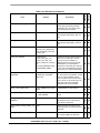
Table 2-5. periphBitSet arguments
Mask
in
Bit mask.
pAddr
in
The memory address.
Description: The periphBitSet macro sets the selected bits in a memory location addressed by parameter
pAddr.
Example 2-20. periphBitSet macro usage
periphBitSet(0xC000, &ArchIO.TimerD.ch0.scr);
This code sets bits 15 and 14 in the timer/counter D0 Status and Control Register (SCR).
2.5.4
periphMemInvBitSet - invert memory content and set selected bits
Call(s):
void periphMemInvBitSet(UWord16 Mask, UWord16 *pAddr);
Arguments:
Table 2-6. periphMemInvBitSet arguments
Mask
in
Bit mask.
DSC56800EX Quick Start User’s Guide, Rev. 2, 04/2015
2-12
Freescale Semiconductor, Inc.
Table 2-6. periphMemInvBitSet arguments
pAddr
in
The memory address.
Description: The periphMemInvBitSet macro reads the memory content, inverts its value and sets the
selected bits in a memory location addressed by parameter pAddr.
Note, that this macro can be used in some special purposes, e.g. for clearing the pending flags.
Example 2-21. periphMemInvBitSet macro usage
periphMemInvBitSet(0x0004, &ArchIO.Sim.rststs);
This code clears the Power On Reset flag in the RSTSTS register.
2.5.5
periphBitClear - clear selected bits
Call(s):
void periphBitClear(UWord16 Mask, UWord16 *pAddr);
Arguments:
Table 2-7. periphBitClear arguments
Mask
in
Bit mask.
pAddr
in
The memory address.
Description: The periphBitClear macro clears the selected bits in a memory location addressed by
parameter pAddr.
Example 2-22. periphBitClear macro usage
periphBitClear(0xC000, &ArchIO.TimerD.ch0.scr);
This code clears bits 15 and 14 in the timer/counter D0 Status and Control Register (SCR).
DSC56800EX Quick Start User’s Guide, Rev. 2, 04/2015
Freescale Semiconductor, Inc.
2-13
2.5.6
periphBitGrpSR - set bit group to given value
Call(s):
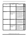
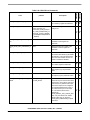
void periphBitGrpSR(UWord16 GroupMask, UWord16 Mask,
UWord16 *pAddr);
Arguments:
Table 2-8. periphBitSet arguments
GroupMask
in
Group mask
Mask
in
“ones” bit mask.
pAddr
in
The memory address.
Description: The periphBitGrpSR macro sets the bit group to a given value in a memory location
addressed by parameter pAddr. All bits specified by GroupMask are affected. These bits are either set if
the corresponding bits in Mask value are also set or they are cleared if the corresponding bits in Mask value
are cleared.
This macro uses a single instruction to execute the operation and allows only constants as GroupMask and
Mask arguments. If the application requires the variable as argument, the periphBitGrpSRVar macro must
be used instead.
Example 2-23. periphBitGrpSR macro usage
periphBitGrpSR(0x007f, 10, &ArchIO.Pll.plldb);
This code sets the lower 7 bits of PLL Divide-By register to the value 10. Other bits in the register are not
affected.
2.5.7
periphBitGrpSRVar - set bit group to given value
Call(s):
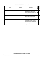
void periphBitGrpSRVar(UWord16 GroupMask, UWord16 Mask,
UWord16 *pAddr);
Arguments:
Table 2-9. periphBitSet arguments
GroupMask
in
Group mask
Mask
in
“ones” bit mask.
pAddr
in
The memory address.
DSC56800EX Quick Start User’s Guide, Rev. 2, 04/2015
2-14
Freescale Semiconductor, Inc.
Description: The periphBitGrpSRVar macro sets the bit group to a given value in a memory location
addressed by parameter pAddr. All bits specified by GroupMask are affected. These bits are either set if
the corresponding bits in Mask value are also set or they are cleared if the corresponding bits in Mask value
are cleared.
The “SR” variant uses two non-interruptible instructions bfset and bfclr to accomplish the requested
operation. The bfset first sets the “one” bits in the destination location, and bfclr then clears the “zero” bits
there.
Caution: This macro is the optimal way how to set the specified group of bits to given value. However, it
must be kept in mind that during the short time between these two bit operations, the target memory
location goes through the third state where the bit group might contain invalid value (“ones” already set
but “zeroes” not yet cleared).
Example 2-24. periphBitGrpSRVar macro usage
periphBitGrpSRVar(0x007f, 10, &ArchIO.Pll.plldb);
This code sets the lower 7 bits of PLL Divide-By register to the value 10. Other bits in the register are not
affected.
2.5.8
periphBitGrpRS - set bit group to given value
Call(s):
void periphBitGrpRS(UWord16 GroupMask, UWord16 Mask,
UWord16 *pAddr);
Arguments:
Table 2-10. periphBitSet arguments
GroupMask
in
Group mask
Mask
in
“ones” bit mask.
pAddr
in
The memory address.
Description: The periphBitGrpRS macro sets the bit group to a given value in a memory location
addressed by parameter pAddr. All bits specified by GroupMask are affected. These bits are either set if
the corresponding bits in Mask value are also set or they are cleared if the corresponding bits in Mask value
are cleared.
This macro uses a single instruction to execute the operation and allows only constants as GroupMask and
Mask arguments. If the application requires the variable as argument, the periphBitGrpRSVar macro must
be used instead.
Example 2-25. periphBitGrpRS macro usage
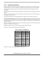
periphBitGrpRS(0x0F00, 0x0100, &ArchIO.Adc1.adctl1);
DSC56800EX Quick Start User’s Guide, Rev. 2, 04/2015
Freescale Semiconductor, Inc.
2-15
This code enables the High Limit exceeded interrupt if the current result value is greater than the high limit.
Other bits in the register are not affected.
2.5.9
periphBitGrpRSVar - set bit group to given value
Call(s):
void periphBitGrpRSVar(UWord16 GroupMask, UWord16 Mask,
UWord16 *pAddr);
Arguments:
Table 2-11. periphBitSet arguments
GroupMask
in
Group mask
Mask
in
“ones” bit mask.
pAddr
in
The memory address.
Description: The periphBitGrpRSVar macro sets the bit group to a given value in a memory location
addressed by parameter pAddr. All bits specified by GroupMask are affected. These bits are either set if
the corresponding bits in Mask value are also set or they are cleared if the corresponding bits in Mask value
are cleared.
The “RS” variant uses two non-interruptible instructions bfclr and bfset to accomplish the requested
operation. The bfclr first clears the “zero” bits in the destination location, and bfclr then sets the “one” bits
there.
Caution: This macro is the optimal way how to set the specified group of bits to given value. However, it
must be kept in mind that during the short time between these two bit operations, the target memory
location goes through the third state where the bit group might contain invalid value (“ones” already set
but “zeroes” not yet cleared).
Example 2-26. periphBitGrpRSVar macro usage
periphBitGrpRSVar(0x0F00, 0x0100, &ArchIO.Adc1.adctl1);
This code enables the High Limit exceeded interrupt if the current result value is greater than the high limit.
Other bits in the register are not affected.
2.5.10
periphBitGrpRS32 - set bit group to given value
Call(s):
void periphBitGrpRS32(UWord32 GroupMask, UWord132 Mask,
UWord16 *pAddr);
Arguments:
DSC56800EX Quick Start User’s Guide, Rev. 2, 04/2015
2-16
Freescale Semiconductor, Inc.
Table 2-12. periphBitSet arguments
GroupMask
in
Group mask
Mask
in
“ones” bit mask.
pAddr
in
The memory address.
Description: The periphBitGrpRS32 macro sets the bit group to a given value in a memory location
addressed by parameter pAddr. All bits specified by GroupMask are affected. These bits are either set if
the corresponding bits in Mask value are also set or they are cleared if the corresponding bits in Mask value
are cleared.
The “RS” variant uses two non-interruptible instructions bfclr and bfset to accomplish the requested
operation. The bfclr first clears the “zero” bits in the destination location, and bfclr then sets the “one” bits
there.
Caution: This macro is the optimal way how to set the specified group of bits to given value. However, it
must be kept in mind that during the short time between these two bit operations, the target memory
location goes through the third state where the bit group might contain invalid value (“ones” already set
but “zeroes” not yet cleared).
Example 2-27. periphBitGrpSR macro usage
periphBitGrpRS32(0x00000007, 3, &ArchIO.FCan.ctrl1);
This code set the length of the Propagation Segment in the bit time. The valid programmable values are
0–7. This field can be written only in Freeze mode because it is blocked by hardware in other modes.Other
bits in the register are not affected.
2.5.11
periphBitGrpZS - set bit group to given value
Call(s):
void periphBitGrpZS(UWord16 GroupMask, UWord16 Mask,
UWord16 *pAddr);
Arguments:
Table 2-13. periphBitSet arguments
GroupMask
in
Group mask
Mask
in
“ones” bit mask.
pAddr
in
The memory address.
Description: The periphBitGrpZS macro sets the bit group to a given value in a memory location
addressed by parameter pAddr. All bits specified by GroupMask are affected. The bits are either set if the
corresponding bits in Mask value are also set or they are cleared if the corresponding bits in Mask value
are cleared.
DSC56800EX Quick Start User’s Guide, Rev. 2, 04/2015
Freescale Semiconductor, Inc.
2-17
This macro uses a single instruction to execute the operation and allows only constants as GroupMask and
Mask arguments. If the application requires the variable as argument, the periphBitGrpZSVar macro must
be used instead.
Example 2-28. periphBitGrpZS macro usage
periphBitGrpZS(0x007f, 10, &ArchIO.Pll.plldb);
This code sets the lower 7 bits of PLL Divide-By register to the value 10. Other bits in the register are not
affected.
2.5.12
periphBitGrpZSVar - set bit group to given value
Call(s):
void periphBitGrpZSVar(UWord16 GroupMask, UWord16 Mask,
UWord16 *pAddr);
Arguments:
Table 2-14. periphBitSet arguments
GroupMask
in
Group mask
Mask
in
“ones” bit mask.
pAddr
in
The memory address.
Description: The periphBitGrpZSVar macro sets the bit group to a given value in a memory location
addressed by parameter pAddr. All bits specified by GroupMask are affected. The bits are either set if the
corresponding bits in Mask value are also set or they are cleared if the corresponding bits in Mask value
are cleared.
The “ZS” variant uses two non-interruptible instructions bfclr and bfset to accomplish the requested
operation. The bfclr first clears all bits in GroupMask and bfset then sets the “one” bits there.
Caution: This macro is the optimal way how to set the specified group of bits to given value. However, it
must be kept in mind that during the short time between these two bit operations, the target memory
location goes through the third state where the bit group contains zeroes.
Example 2-29. periphBitGrpZSVar macro usage
periphBitGrpZSVar(0x007f, 10, &ArchIO.Pll.plldb);
This code sets the lower 7 bits of PLL Divide-By register to the value 10. Other bits in the register are not
affected.
DSC56800EX Quick Start User’s Guide, Rev. 2, 04/2015
2-18
Freescale Semiconductor, Inc.
2.5.13
periphBitGrpSet - set bit group to given value
Call(s):
void periphBitGrpSet(UWord16 GroupMask, UWord16 Mask,
UWord16 *pAddr);
Arguments:
Table 2-15. periphBitSet arguments
GroupMask
in
Group mask
Mask
in
“ones” bit mask.
pAddr
in
The memory address.
Description: The periphBitGrpSet macro sets the bit group to a given value in a memory location
addressed by parameter pAddr. All bits specified by GroupMask are affected. The bits are either set if the
corresponding bits in Mask value are also set or they are cleared if the corresponding bits in Mask value
are cleared.
This macro uses a single instruction to execute the operation and allows only constants as GroupMask and
Mask arguments. If the application requires the variable as argument, the periphBitGrpSetVar macro must
be used instead.
Example 2-30. periphBitGrpSet macro usage
periphBitGrpSet(0x007f, 10, &ArchIO.Pll.plldb);
This code sets the lower 7 bits of PLL Divide-By register to the value 10. Other bits in the register are not
affected (but see “Caution” above).
2.5.14
periphBitGrpSetVar - set bit group to given value
Call(s):
void periphBitGrpSetVar(UWord16 GroupMask, UWord16 Mask,
UWord16 *pAddr);
Arguments:
Table 2-16. periphBitSet arguments
GroupMask
in
Group mask
Mask
in
“ones” bit mask.
pAddr
in
The memory address.
DSC56800EX Quick Start User’s Guide, Rev. 2, 04/2015
Freescale Semiconductor, Inc.
2-19
Description: The periphBitGrpSetVar macro sets the bit group to a given value in a memory location
addressed by parameter pAddr. All bits specified by GroupMask are affected. The bits are either set if the
corresponding bits in Mask value are also set or they are cleared if the corresponding bits in Mask value
are cleared.
This variant uses the accumulator and read-modify-write instructions to accomplish the requested
operation. The memory location is first read to accumulator, the bfclr and bfset instructions are performed
on accumulator and the result value is then written back to memory location.
Caution: It might seem this macro is the “proper” way how to set the group of bits to certain value as there
are no intermediate invalid values written in the target memory location. However, it is quite dangerous to
use this macro when interrupts may occur between the read and write operations. If the interrupt service
routine would write the other portion of the target memory location, the written value could be overwritten
back with its previous state by the write accumulator operation of periphBitGrpSetVar.
Example 2-31. periphBitGrpSetVar macro usage
periphBitGrpSetVar(0x007f, 10, &ArchIO.Pll.plldb);
This code sets the lower 7 bits of PLL Divide-By register to the value 10. Other bits in the register are not
affected (but see “Caution” above).
2.5.15
periphBitGrpSet32 - set bit group to given value
Call(s):
void periphBitGrpSet(UWord32 GroupMask, UWord32 Mask,
UWord16 *pAddr);
Arguments:
Table 2-17. periphBitSet arguments
GroupMask
in
Group mask
Mask
in
“ones” bit mask.
pAddr
in
The memory address.
Description: The periphBitGrpSet32 macro sets the bit group to a given value in a memory location
addressed by parameter pAddr. All bits specified by GroupMask are affected. The bits are either set if the
corresponding bits in Mask value are also set or they are cleared if the corresponding bits in Mask value
are cleared.
This variant uses the accumulator and read-modify-write instructions to accomplish the requested
operation. The memory location is first read to accumulator, the bfclr and bfset instructions are performed
on accumulator and the result value is then written back to memory location.
DSC56800EX Quick Start User’s Guide, Rev. 2, 04/2015
2-20
Freescale Semiconductor, Inc.
Caution: It might seem this macro is the “proper” way how to set the group of bits to certain value as there
are no intermediate invalid values written in the target memory location. However, it is quite dangerous to
use this macro when interrupts may occur between the read and write operations. If the interrupt service
routine would write the other portion of the target memory location, the written value could be overwritten
back with its previous state by the write accumulator operation of periphBitGrpSet32.
Example 2-32. periphBitGrpSet macro usage
periphBitGrpSet32(0x0C0000000, 0x040000000, &ArchIO.crc.ctrl);
This code sets the lower TOT bit 30 of CRC Control register. Other bits in the register are not affected (but
see “Caution” above).
2.5.16
periphSafeAckByOne - clear (acknowledge) bit flags which are
active-high and are cleared by write-one
Call(s):
void periphSafeAckByOne(UWord16 GroupMask, UWord16 Mask,
UWord16 *pAddr);
Arguments:
Table 2-18. periphSafeAckByOne arguments
GroupMask
in
Group mask
Mask
in
“ones” bit mask.
pAddr
in
The memory address.
Description: The periphSafeAckByOne macro clears (acknowledges) bit flags which are active-high and
are cleared by write-one in a peripheral memory location addressed by parameter pAddr. The GroupMask
specifies all flags which might be affected by clearing procedure. The Mask value specifies flag/flags to
be cleared.
This macro uses a single instruction to execute the operation and allows only constants as GroupMask and
Mask arguments. If the application requires the variable as argument, the periphSafeAckByOneVar macro
must be used instead.
Example 2-33. periphSafeAckByOne macro usage
periphSafeAckByOne(0x8000 | 0x0100 | 0x0010, 0x0100,
&ArchIO.Decoder0.deccr);
This code clears the Index Pulse Interrupt Request flag in the Decoder Control Register.
DSC56800EX Quick Start User’s Guide, Rev. 2, 04/2015
Freescale Semiconductor, Inc.
2-21
2.5.17
periphSafeAckByOneVar - clear (acknowledge) bit flags which are
active-high and are cleared by write-one
Call(s):
void periphSafeAckByOneVar(UWord16 GroupMask, UWord16 Mask,
UWord16 *pAddr);
Arguments:
Table 2-19. periphSafeAckByOneVar arguments
GroupMask
in
Group mask
Mask
in
“ones” bit mask.
pAddr
in
The memory address.
Description: The periphSafeAckByOneVar macro clears (acknowledges) bit flags which are active-high
and are cleared by write-one in a peripheral memory location addressed by parameter pAddr. The
GroupMask specifies all flags which might be affected by clearing procedure. The Mask value specifies
flag/flags to be cleared.
Caution: TBD
Example 2-34. periphSafeAckByOneVar macro usage
periphSafeAckByOne(0x8000 | 0x0100 | 0x0010, 0x0100,
&ArchIO.Decoder0.deccr);
This code clears the Index Pulse Interrupt Request flag in the Decoder Control Register.
2.5.18
periphSafeBitClear - clear bits and keep value of bit flags which are
cleared by write-one
Call(s):
void periphSafeBitClear(UWord16 FlagGroupMask, UWord16 Mask,
UWord16 *pAddr);
Arguments:
Table 2-20. periphSafeBitClear arguments
FlagGroupMask
in
Group mask of bit flags which are cleared by write-one
Mask
in
bit mask.
pAddr
in
The memory address.
DSC56800EX Quick Start User’s Guide, Rev. 2, 04/2015
2-22
Freescale Semiconductor, Inc.
Description: The periphSafeBitClear macro clears the selected bits and keeps value of the bit flags which
are cleared by write-one in a peripheral memory location addressed by parameter pAddr. The
FlagGroupMask specifies all flags which are cleared by write-one. The Mask value specifies bit/bits to be
cleared.
Caution: TBD
Example 2-35. periphSafeBitClear macro usage
periphSafeBitClear(0x0002 | 0x0010, 0x0004, &ArchIO.HscmpA.scr);
This code disables the falling edge HSCMP A module. The rising edge and falling edge interrupt flags are
not cleared
2.5.19
periphSafeBitSet - Set bits and keep value of bit flags which are
cleared by write-one
Call(s):
void periphSafeBitSet(UWord16 FlagGroupMask, UWord16 Mask,
UWord16 *pAddr);
Arguments:
Table 2-21. periphSafeBitSet arguments
FlagGroupMask
in
Group mask of bit flags which are cleared by write-one
Mask
in
bit mask.
pAddr
in
The memory address.
Description: The periphSafeBitSet macro sets the selected bits and keeps value of the bit flags which are
cleared by write-one in a peripheral memory location addressed by parameter pAddr. The FlagGroupMask
specifies all flags which are cleared by write-one. The Mask value specifies bit/bits to be set.
This macro uses a single instruction to execute the operation and allows only constants as GroupMask and
Mask arguments. If the application requires the variable as argument, the periphSafeBitSetVar macro must
be used instead.
Example 2-36. periphSafeBitSet macro usage
periphSafeBitSet(0x0002 | 0x0004, 0x0010, &ArchIO.HscmpA.scr);
This code enables the rising edge HSCMP A module. The rising edge and falling edge interrupt flags are
not cleared
DSC56800EX Quick Start User’s Guide, Rev. 2, 04/2015
Freescale Semiconductor, Inc.
2-23
2.5.20
periphSafeBitSetVar - Set bits and keep value of bit flags which are
cleared by write-one
Call(s):
void periphSafeBitSetVar(UWord16 FlagGroupMask, UWord16 Mask,
UWord16 *pAddr);
Arguments:
Table 2-22. periphSafeBitSetVar arguments
FlagGroupMask
in
Group mask of bit flags which are cleared by write-one
Mask
in
bit mask.
pAddr
in
The memory address.
Description: The periphSafeBitSetVar macro sets the selected bits and keeps value of the bit flags which
are cleared by write-one in a peripheral memory location addressed by parameter pAddr. The
FlagGroupMask specifies all flags which are cleared by write-one. The Mask value specifies bit/bits to be
set.
Caution: It might seem this macro is the “proper” way how to set the group of bits to certain value as there
are no intermediate invalid values written in the target memory location. However, it is quite dangerous to
use this macro when interrupts may occur between the read and write operations. If the interrupt service
routine would write the other portion of the target memory location, the written value could be overwritten
back with its previous state by the write accumulator operation of periphBitGrpSet.
Example 2-37. periphSafeBitSetVar macro usage
periphSafeBitSetVar(0x0002 | 0x0004, 0x0010, &ArchIO.HscmpA.scr);
This code enables the rising edge HSCMP A module. The rising edge and falling edge interrupt flags are
not cleared
2.5.21
periphSafeBitSet32 - Set bits and keep value of bit flags which are
cleared by write-one
Call(s):
void periphSafeBitSet(UWord32 FlagGroupMask, UWord32 Mask,
UWord16 *pAddr);
Arguments:
Table 2-23. periphSafeBitSet arguments
FlagGroupMask
in
Group mask of bit flags which are cleared by write-one
Mask
in
bit mask.
DSC56800EX Quick Start User’s Guide, Rev. 2, 04/2015
2-24
Freescale Semiconductor, Inc.
Table 2-23. periphSafeBitSet arguments
pAddr
in
The memory address.
Description: The periphSafeBitSet32 macro sets the selected bits and keeps value of the bit flags which
are cleared by write-one in a peripheral memory location addressed by parameter pAddr. The
FlagGroupMask specifies all flags which are cleared by write-one. The Mask value specifies bit/bits to be
set.
Caution: It might seem this macro is the “proper” way how to set the group of bits to certain value as there
are no intermediate invalid values written in the target memory location. However, it is quite dangerous to
use this macro when interrupts may occur between the read and write operations. If the interrupt service
routine would write the other portion of the target memory location, the written value could be overwritten
back with its previous state by the write accumulator operation of periphBitGrpSet32.
Example 2-38. periphSafeBitSet macro usage
periphSafeBitSet32(0x080808000, 0x000000080,&ArchIO.dma.reqc);
Clears the state machine for DMA channel 3.
2.5.22
periphSafeBitGrpSet - set bit group to given value and keep value of
bit flags which are cleared by write-one
Call(s):
void periphSafeBitGrpSet(UWord16 FlagGroupMask,
UWord16 GroupMask, UWord16 Mask,
UWord16 *pAddr);
Arguments:
Table 2-24. periphSafeBitGrpSet arguments
FlagGroupMask
in
Group mask of bit flags which are cleared by write-one
GroupMask
in
Group mask
Mask
in
bit mask.
pAddr
in
The memory address.
Description: The periphSafeBitGrpSet macro sets bit group to given value and keeps value of the bit flags
which are cleared by write-one in a peripheral memory location addressed by parameter pAddr. The
FlagGroupMask specifies all flags which are cleared by write-one. All bits specified by GroupMask are
affected. The bits are either set if the corresponding bits in Mask value are also set or they are cleared if
the corresponding bits in Mask value are cleared.
DSC56800EX Quick Start User’s Guide, Rev. 2, 04/2015
Freescale Semiconductor, Inc.
2-25
This macro uses a single instruction to execute the operation and allows only constants as GroupMask and
Mask arguments. If the application requires the variable as argument, the periphSafeBitGrpSetVar macro
must be used instead.
Example 2-39. periphSafeBitGrpSet macro usage
periphSafeBitGrpSet(0x0002 | 0x0004, 0x00C0, 0x0040, &ArchIO.HscmpA.scr);
This code sets the HSCMP A module input hysteresis to 1. The rising edge and falling edge interrupt flags
are not cleared
2.5.23
periphSafeBitGrpSetVar - set bit group to given value and keep
value of bit flags which are cleared by write-one
Call(s):
void periphSafeBitGrpSetVar(UWord16 FlagGroupMask,
UWord16 GroupMask, UWord16 Mask,
UWord16 *pAddr);
Arguments:
Table 2-25. periphSafeBitGrpSetVar arguments
FlagGroupMask
in
Group mask of bit flags which are cleared by write-one
GroupMask
in
Group mask
Mask
in
bit mask.
pAddr
in
The memory address.
Description: The periphSafeBitGrpSetVar macro sets bit group to given value and keeps value of the bit
flags which are cleared by write-one in a peripheral memory location addressed by parameter pAddr. The
FlagGroupMask specifies all flags which are cleared by write-one. All bits specified by GroupMask are
affected. The bits are either set if the corresponding bits in Mask value are also set or they are cleared if
the corresponding bits in Mask value are cleared.
Caution: It might seem this macro is the “proper” way how to set the group of bits to certain value as there
are no intermediate invalid values written in the target memory location. However, it is quite dangerous to
use this macro when interrupts may occur between the read and write operations. If the interrupt service
routine would write the other portion of the target memory location, the written value could be overwritten
back with its previous state by the write accumulator operation of periphBitGrpSetVar.
Example 2-40. periphSafeBitGrpSetVar macro usage
periphSafeBitGrpSet(0x0002 | 0x0004, 0x00C0, 0x0040, &ArchIO.HscmpA.scr);
DSC56800EX Quick Start User’s Guide, Rev. 2, 04/2015
2-26
Freescale Semiconductor, Inc.
This code sets the HSCMP A module input hysteresis to 1. The rising edge and falling edge interrupt flags
are not cleared
2.5.24
periphSafeBitGrpSet32 - set bit group to given value and keep value
of bit flags which are cleared by write-one
Call(s):
void periphSafeBitGrpSet(UWord32 FlagGroupMask,
UWord32 GroupMask, UWord32 Mask,
UWord16 *pAddr);
Arguments:
Table 2-26. periphSafeBitGrpSet arguments
FlagGroupMask
in
Group mask of bit flags which are cleared by write-one
GroupMask
in
Group mask
Mask
in
bit mask.
pAddr
in
The memory address.
Description: The periphSafeBitGrpSet32 macro sets bit group to given value and keeps value of the bit
flags which are cleared by write-one in a peripheral memory location addressed by parameter pAddr. The
FlagGroupMask specifies all flags which are cleared by write-one. All bits specified by GroupMask are
affected. The bits are either set if the corresponding bits in Mask value are also set or they are cleared if
the corresponding bits in Mask value are cleared.
Caution: It might seem this macro is the “proper” way how to set the group of bits to certain value as there
are no intermediate invalid values written in the target memory location. However, it is quite dangerous to
use this macro when interrupts may occur between the read and write operations. If the interrupt service
routine would write the other portion of the target memory location, the written value could be overwritten
back with its previous state by the write accumulator operation of periphBitGrpSet32.
Example 2-41. periphSafeBitGrpSet macro usage
periphSafeBitGrpSet32(0x080808080, 0x00F000000, 1 ,&ArchIO.dma.reqc);
This code selects the request 1 as the DMA source.
DSC56800EX Quick Start User’s Guide, Rev. 2, 04/2015
Freescale Semiconductor, Inc.
2-27
2.5.25
periphBitChange - change selected bits
Call(s):
void periphBitChange(UWord16 Mask, UWord16 *pAddr);
Arguments:
Table 2-27. periphBitChange arguments
Mask
in
Bit mask.
pAddr
in
The memory address.
Description: The periphBitChange macro complements the selected bits in a memory location addressed
by parameter pAddr.
Example 2-42. periphBitChange macro usage
periphBitChange(0xC000, &ArchIO.PortB.dr);
This code complements bits 15 and 14 in the Port B Data Register (DR).
2.5.26
periphBitTest - test selected bits
Call(s):
UWord16 periphBitTest(UWord16 Mask, UWord16 *pAddr);
Arguments:
Table 2-28. periphBitTest arguments
Mask
in
Bit mask.
pAddr
in
The memory address.
Description: The periphBitTest macro tests the selected bits if they are set in a memory location addressed
by parameter pAddr.
Example 2-43. periphBitTest macro usage
if (periphBitTest(0x8000, &ArchIO.TimerD.ch0.scr))
{
periphBitClear(0x8000, &ArchIO.TimerD.ch0.scr);
};
This code checks if Timer Compare Flag (Bit 15) in the timer/counter D0 Status and Control Register
(SCR) is set.
DSC56800EX Quick Start User’s Guide, Rev. 2, 04/2015
2-28
Freescale Semiconductor, Inc.
2.5.27
periphMemDummyRead - memory dummy read
Call(s):
void periphMemDummyRead(UWord16 *pAddr);
Arguments:
Table 2-29. periphMemDummyRead arguments
pAddr
in
The memory address from which to read a 16-bit word.
Description: The periphMemDummyRead macro reads a 16-bit word from the memory location addressed
by parameter pAddr. The result is thrown away.
Example 2-44. periphMemDummyRead macro usage
periphMemDummyRead(&ArchIO.Sci.scisr);
This code reads the SCI status register to clear SCI flags.
2.5.28
periphMemForcedRead- memory force read (Never optimized out)
Call(s):
UWord16 periphMemForcedRead(UWord16 *pAddr);
Arguments:
Table 2-30. periphMemForcedRead arguments
pAddr
in
The memory address from which to read a 16-bit word.
Description: The periphMemForcedRead macro reads a 16-bit word from the memory location addressed
by parameter pAddr. This macro is never optimized out.
Example 2-45. periphMemForcedRead macro usage
periphMemForcedRead(&ArchIO.Sci.scisr);
This code reads the SCI status register to clear SCI flags.
2.5.29
Miscellaneous Routines
This section describes some additional routines provided by the 56800EX_Quick_Start tool.
DSC56800EX Quick Start User’s Guide, Rev. 2, 04/2015
Freescale Semiconductor, Inc.
2-29
2.5.29.1
impyuu - integer multiply unsigned 16b x unsigned 16b
Call(s):
UWord32 impyuu(UWord16 unsigA, UWord16 unsigB);
Arguments:
Table 2-31. impyuu arguments
unsigA
in
first argument
unsigB
in
second argument
Description: The impyuu inline function multiplies a 16-bit unsigned integer with a 16-bit unsigned
integer and returns the 32-bit unsigned integer result.
Returns: result of multiplication unsigA unsigB
Example 2-46. impyuu function usage
UWord16 var1 = 65535U;
UWord16 var2 = 65535U;
UWord32 result;
result = impyuu(var1, var2); /* returns 4294836225 */
This code multiplies variables var1 and var2 and returns the result in result variable.
2.5.29.2
impysu - integer multiply signed 16b x unsigned 16b
Call(s):
Word32 impysu(Word16 sig, UWord16 unsig);
Arguments:
Table 2-32. impysu arguments
sig
in
first argument (signed)
unsig
in
second argument (unsigned)
Description: The impysu function multiplies 16-bit signed integer and 16-bit unsigned integer as an and
returns the 32-bit signed integer result.
Returns: result of multiplication sig unsig
Example 2-47. impysu function usage
Word16 var1 = -32768;
DSC56800EX Quick Start User’s Guide, Rev. 2, 04/2015
2-30
Freescale Semiconductor, Inc.
UWord16 var2 = 65535U;
Word32 result;
result = impysu(var1, var2); /* returns -2147450880 */
This code multiplies variables var1 and var2 and returns the result in result variable.
2.5.29.3
shl2 - optimized version of shl intrinsic function
Call(s):
Word16 shl2(Word16 num, UWord16 shifts);
Arguments:
Table 2-33. shl2 arguments
num
in
parameter to be shifted
shifts
in
number of shifts
Description: The shl2 function performs a multi-bit arithmetic shift of the first parameter to the left by the
amount specified in the second parameter. The result is returned as a 16-bit integer. This function is the
optimized version of the shl intrinsic function (see CodeWarrior Help for more information on shl).
Returns: num parameter shifted shifts times to the left
Example 2-48. shl2 function usage
Word16 var1 = 1;
UWord16 var2 = 15;
Word16 result;
result = shl2(var1, var2); /* returns 0x8000 */
This code shifts var1 variable var2 times to the left and returns the result in result variable.
2.5.29.4
shr2 - optimized version of shr intrinsic function
Call(s):
Word16 shr2(Word16 num, UWord16 shifts);
Arguments:
Table 2-34. shr2 arguments
num
in
parameter to be shifted
DSC56800EX Quick Start User’s Guide, Rev. 2, 04/2015
Freescale Semiconductor, Inc.
2-31
Table 2-34. shr2 arguments
shifts
in
number of shifts
Description: The shr2 function performs a multi-bit arithmetic shift of the first parameter to the right by
the amount specified in the second parameter. The result is returned as a 16-bit integer. This function is the
optimized version of the shr intrinsic function (see CodeWarrior Help for more information on shr).
Returns: num parameter shifted shifts times to the right
Example 2-49. shr2 function usage
Word16 var1 = 16;
Word16 result;
result = shr2(var1, 3); /* returns 0x0002 */
This code shifts var1 variable three times to the right and returns the result in the result variable.
2.5.30
Intrinsic Functions
The 56800EX_Quick_Start tool can exploit the system intrinsic functions defined in intrinsics_56800E.h
header file distributed with the CodeWarrior Development Studio 56800/EX Hybrid Controllers.
To preserve compatibility with the DSP56800_Quick_Start tool, the intrinsics_56800E.h is included in
core.h header file, if the macro __MWERKS__ is defined.
2.6
Interrupts
This section describes interrupt processing and interrupt configuration using the 56800EX_Quick_Start
tool. For detailed information on interrupts and interrupt processing for the 56F800EX, please see the
DSP56800E and DSP56800EX Reference Manual and the target processor’s Reference Manual.
2.6.1
Processing Interrupts
An interrupt is an event that is generated by a condition inside the microcontroller or from external sources.
When such event occurs, the interrupt processing transfers control from the currently executing program
to an interrupt service routine (ISR), with the ability to later return to the current program upon completion
of the ISR. Among the main uses of interrupts we can have data transfers between microcontroller memory
and a peripheral device, or begin of execution of an algorithm upon reception of a new sample. An
interrupt can also be used, for example, to exit the microcontroller’s low-power wait processing state.
2.6.1.1
Interrupt Vector Table
The interrupt system on 56F800E can be defined as vectored. Each interrupt source has its own program
memory location at a fixed address, to which program control is passed when an interrupt occurs. This
DSC56800EX Quick Start User’s Guide, Rev. 2, 04/2015
2-32
Freescale Semiconductor, Inc.
program memory location must contain a JSR instruction with the address of the interrupt service routine
(ISR). When this interrupt occurs, the JSR instruction is executed and the program control is passed to the
ISR. The program memory containing the JSR instructions with the addresses of the ISR is called interrupt
vector table.
The interrupt vector table might be located at base address 0x0000. During the code execution, the
interrupt vector table base address can be changed by modifying the VBA register of interrupt controller
unit (INTC).
In the 56800EX_Quick_Start tool, the full interrupt vector table is always located at address 0x0000. The
VBA register is set to zero during the startup code. See Section 2.1.1 on page -2 for closer description of
the booting process.
In the 56800EX_Quick_Start tool, the interrupt vector table is implemented in C code which enables to
effectively use the C preprocessor. The special macros defined in the global application configuration file
(appconfig.h) can be used to setup the interrupt vector and to assign the interrupt priorities.
The interrupt controller and its configuration are described in more details later in Section .
2.6.1.2
Interrupt Processing Flow
Figure 2-2 shows an interrupt processing flow. The 56800EX_Quick_Start tool does not provide any
intermediate step when calling the ISR. When an interrupt occurs, the currently executed program is
interrupted and the JSR instruction from the interrupt vector table is fetched. Executing the JSR instruction
results in the program changing its flow directly to an ISR. Also the status register and the program counter
are pushed onto the stack. When the user ISR finishes, it executes a Return from Interrupt (RTI)
instruction, which pops the program counter and the status register from the hardware stack. It puts the
User Code back into the same state as it was in before execution, assuming that the User ISR saved and
restored all the registers it had used.
DSC56800EX Quick Start User’s Guide, Rev. 2, 04/2015
Freescale Semiconductor, Inc.
2-33
Interrupt Vector Table
in Program Memory
JSR
Interrupt
Occurs
Isr1
JSR
Isr2
user code
Isr2()
PC and SR
saved
1) save used registers
2) user code
3) restore registers
4) RTI
JSR
Isr3
Return from Interrupt (PC and SR restored)
Figure 2-2. Interrupt Processing Flow
2.6.1.3
ISRs
An ISR is a program code that is executed when an interrupt is detected. An ISR is responsible for
servicing the cause of the interrupt, such as reading a sample from a port when it is full or transmitting a
sample to a port when it is empty. When an interrupt occurs, all other interrupts of the same or of a lower
priority are disabled from executing, until the current ISR finishes executing. For this reason, an ISR
should be as fast as possible to prevent any overflow or under run condition.
Inside the ISR it is necessary to save, and upon servicing the interrupt, to restore all used registers,
including registers from the register bank used by the compiler. The 56800EX_Quick_Start tool does not
provide any automatic saving/restoring of used registers.
The last instruction of an ISR must be “Return from Interrupt” (RTI) instruction. This instruction restores
the SR and the PC from the stack.
Both saving/restoring registers and using RTI instead of RTS are provided by the compiler directive
#pragma interrupt. #pragma interrupt is used when declaring a C function and it instructs the compiler to
save all registers used within a C function and to restore those register values upon exiting. Also it places
an RTI instruction instead of an RTS at the end of the function. See Section 2.6.3.
2.6.1.4
Interrupt Priority Levels
On 56F800EX hybrid microcontroller family, each interrupt can be assigned the interrupt priority level
(IPL). It is the number from 0 (lowest priority) to 3 (highest priority). When servicing the interrupt, until
the RTI instruction is executed, the other interrupts of the same and lower priority levels are masked
DSC56800EX Quick Start User’s Guide, Rev. 2, 04/2015
2-34
Freescale Semiconductor, Inc.
(temporarily disabled). If there is an interrupt request of the masked priority level, its processing is
postponed until the level is unmasked again.
This model assures that the interrupts of the same level can not “nest” one to each other. On the other hand,
the higher priority interrupts do nest to the lower priority interrupts.
2.6.1.5
Fast Interrupts
Up to 2 interrupt sources can be declared as Fast Interrupts. The Fast Interrupts jump directly to a service
routine based on values in the Fast Interrupt Vector Address registers without having to go to a jump table
first.
IRQs used as fast interrupts MUST be set to priority level 2. Unexpected results can occur if a fast interrupt
vector is set to any other priority.
Caution: A special Fast Interrupt Return instruction (frtid) must be used in order to return from the Fast
Interrupt service routine. There are also several limitations in the way how the Fast Interrupt service
routine can be coded. See the 56800E and 56800EX Reference Manual for more details.
2.6.1.6
Clearing Interrupt Flags
Each on-chip peripheral interrupt source has its own interrupt flag, which must be cleared after the
interrupt is serviced. For each peripheral module, the method of clearing the interrupt flag is different. As
the 56800EX_Quick_Start tool does not add any infrastructure code to the interrupt service routines, it also
does not clear the interrupt flag inside the ISR. See Example 2-50.
Example 2-50. Clearing Interrupt Flags inside ISR
/*******************************************************************************
PWM A Reload Interrupt Service Routine
********************************************************************************/
#pragma interrupt
void pwmAReloadISR(void)
{
/* ISR code */
...
/* clear Reload interrupt flag */
ioctl(PWM_A, PWM_CLEAR_RELOAD_FLAG, NULL);
}
This example shows the PWMA Reload Interrupt Service Routine. Note that the PWM_CLEAR_
RELOAD_FLAG ioctl() command is used to clear the Reload Interrupt Flag (Bit 5) in the PWM Control
Register and that this is the user’s responsibility.
2.6.2
Configuring Interrupts
This section describes the configuration of interrupts using the 56800EX_Quick_Start tool. Interrupt
configuration consists of installing the interrupt service routine (ISR) at the specified interrupt vector,
enabling the interrupt and setting the interrupt priority level.
Installing ISRs
DSC56800EX Quick Start User’s Guide, Rev. 2, 04/2015
Freescale Semiconductor, Inc.
2-35
The 56800EX_Quick_Start tool supports static (compile-time) installation of the ISRs, dynamic
installation (run-time) is not supported. In general, static installation of ISRs requires less program
memory and has a lower (or even no) time overhead.
The static installation of ISRs consists of writing the address of the ISR to the interrupt vector table for
given interrupt source at compilation time. The interrupt vector table is located in the vectors.c file. By
default all interrupt vectors are initialized with the address of the unhandled_interrupt() function in the
vectors.c file, which contains the debughlt instruction and provides an alarm to the user, that this interrupt
was not installed but has occurred, which is very useful when debugging. One exception to this is the
Hardware Reset vector, which contains the address of the startup code - Start() routine in the startup.c file.
To install a user’s ISR at the xxth interrupt vector add the following #define in appconfig.h:
#define INT_VECTOR_ADDR_xx userISRname
The conditional compilation then forces the compiler to use the userISRname() ISR instead of the default
unhandled_interrupt() at the position of the xxth interrupt vector in the interrupt vector table. The
userISRname is the placeholder for the name of interrupt service routine with prototype of
void userISRroutine (void)
In your source code, you then put the following code:
#pragma interrupt
void userISRname(void)
{
/* ISR code */
}
The range of interrupt vectors which can be installed (xx) is 1 to 80. Vector 0 is the Hardware Reset vector
and always refers to the Start() code.
2.6.2.1
Assigning Interrupt Priority Levels
As described in Section 2.6.1.4 on page -34, each enabled interrupt can be assigned to one interrupt priority
level in range from 0 to 3.
There are some exceptions from this rule for the particular interrupt sources which has assigned a fixed
priority levels. Also, as there are only two bits (four combinations) to encode five different states of the
interrupt source (disabled, level 0,..., level 3) there is always one priority level, which cannot be set for any
interrupt.
The 56800EX_Quick_Start tool hides these difficulties and implementation details described above and
simplifies the configuration of the interrupt priority levels to the maximal extent (while keeping the
generated code optimal).
To enable the interrupt servicing and to assign a certain priority level, the user defines the macro:
INT_PRIORITY_LEVEL_xx INTC_LEVELn
To explicitly disable the interrupt, the user can define the macro as
INT_PRIORITY_LEVEL_xx INTC_DISABLED
DSC56800EX Quick Start User’s Guide, Rev. 2, 04/2015
2-36
Freescale Semiconductor, Inc.
where xx is the interrupt number (from 1 to 110) and n is the interrupt level (from 0 to 3). The interrupt
sources configurations are then applied to a processor core by issuing the INTC_INIT ioctl command,
for example in the main function.
The C preprocessor and compiler check the validity of the selected priority level early during the
compilation and issues compilation errors if invalid combination of interrupt source number and interrupt
priority level is requested (or if priority level is requested to be set for the source with fixed priority level).
2.6.2.2
Installing Fast Interrupts
As described in Section 2.6.1.5 on page -35, two interrupt sources can be selected as “Fast Interrupts”. For
the fast interrupts, the interrupt controller does not fetch the jsr instruction from the vector table and
directly loads the program counter (PC) with address specified in dedicated Fast Interrupt Vector Address
(FIVA) registers.
In the 56800EX_Quick_Start tool, the fast interrupts are automatically configured by the INTC_INIT
code if the user defines the macros:
INTC_FIM0_INIT xx
or
INTC_FIM1_INIT xx
where xx specifies what interrupt source is to be selected as fast interrupt (0 or 1).
By default, the address of interrupt service routine defined by INT_VECTOR_ADDR_xx is then
automatically loaded into the FIVA registers during the INTC_INIT command. The preprocessor also
verifies the interrupt identified for a fast interrupt is configured to priority level 2 (which is required for
the proper operation).
Caution: A special Fast Interrupt Return instruction (frtid) must be used in order to return from the Fast
Interrupt service routine.
If there is another vector address to be used for the fast interrupt processing, instead of the default
INT_VECTOR_ADDR_xx, the following macros can be defined in appconfig.h
INTC_FIVA0_INIT fastint0ISR
or
INTC_FIVA1_INIT fastint1ISR
where fastint0ISR and fastint1ISR are the placeholders for the fast interrupt service routine
names.
2.6.2.3
Enabling Interrupts
In addition to the interrupt controller peripheral described above, the 56800EX core has its own method
how to enable and disable the interrupts of certain priority levels. So, regardless the interrupt setting
defined by macros in appconfig.h and initialization done by the INTC_INIT command, there is another
step to do to enable interrupt servicing in the application.
At the core level, the interrupts can be in four states:
DSC56800EX Quick Start User’s Guide, Rev. 2, 04/2015
Freescale Semiconductor, Inc.
2-37
•
•
•
•
All interrupts disabled (default state) - use archDisableInt() macro
All interrupts enabled - use archEnableInt() macro
Priority levels 1, 2 and 3 enabled, level 0 disabled - use archEnableIntLvl123() macro
Priority levels 2 and 3 enabled, levels 0 and 1 disabled - use archEnableIntLvl23() macro
2.6.3
Code Example
The following example shows the installation of the ISR into the interrupt vector table and shows how to
enable interrupts using the 56800EX_Quick_Start tool.
The following example shows the installation of the external interrupt IRQA, the timer/counter D2
interrupt and the PWM A reload interrupt. The example shows a part of the code, which must be included
in appconfig.h, all three ISRs and the initialization code. ISRs are declared as #pragma interrupt to instruct
the compiler to save/restore all used registers and to terminate the ISRs with an RTI instruction. Inside the
appconfig.h file, INT_VECTOR_ADDR_xx and ITCN_INT_PRIORITY_xx define statements are used
to install the ISR at the specified interrupt vector and to define the interrupt priority level. The
achEnableInt() macro and the ITCN driver commands ITCN_INIT_GPRS and ITCN_INIT_IPR are used
to enable interrupts.
Example 2-51. Installing ISRs and enabling interrupts
1) appconfig.h file
/*******************************************************************************
*
* File Name: appconfig.h
*
* Description: file for static configuration of the application
*
(initial values, interrupt vectors)
*
*****************************************************************************/
#ifndef __APPCONFIG_H
#define __APPCONFIG_H
/*.*************************************************************************
*
* File generated by Graphical Configuration Tool Thu, 18/Apr/2013, 10:30:51
*
****************************************************************************.*/
#define
#define
#define
#define
MC56F82748
EXTCLK 8000000L
APPCFG_DFLTS_OMITTED 1
APPCFG_GCT_VERSION 0x02060200L
/*.
OCCS Configuration
-------------------------------------------Use Factory Trim Value: Yes
DSC56800EX Quick Start User’s Guide, Rev. 2, 04/2015
2-38
Freescale Semiconductor, Inc.
Enable internal 32 kHz oscillator: No
Power Down crystal oscillator: Yes
Core frequency: 50 MHz
VCO frequency: 200 MHz
Loss of lock interrupt 0: Disable
Loss of lock interrupt 1: Disable
Loss of reference clock Interrupt: Disable
.*/
#define
#define
#define
#define
OCCS_CTRL_INIT
OCCS_DIVBY_INIT
OCCS_USE_FACTORY_TRIM
OCCS_USE_FACTORY_TRIM_TEMP
0x0081U
0x2018U
1
1
/*.
SYS Configuration
-------------------------------------------SIM: Power Saving Modes: Stop enabled
Wait enabled
OnCE clock to processor core: Enabled when core TAP enabled
DMA Enable in RUN and WAIT modes: DMA enabled in all power modes
Enable External Reset Padcell Input Filter : No , SIM - Clock on GPIO: Enable CLKO_0: No
SIM - Clock on GPIO: Enable CLKO_1: No
SIM - HS_PERF Peripheral Clk: PWM
SIM - Peripheral Clock Enable: GPIO F: Yes, GPIO E: Yes, GPIO D: No , GPIO C: Yes,
GPIO B: No , GPIO A: No , TMR A0: No
TMR A1: No , TMR A2: No , TMR A3: No , SCI0: No , SCI1:
No , QSPI0: No , QSPI1: No , IIC: No , MSCAN: No
CMP A: No , CMP B: No , CMP C: No , CMP D: No , CYC
ADC: No , CRC: No , QDC: No , PIT0: No , PIT1: No , DACA: No , DACB: No
PWMCH0: No , PWMCH1: No , PWMCH2: No , PWMCH3: No ,
SIM - Modules Enabled in Stop: GPIO F: No , SIM - Modules Enabled in Stop: GPIO E: No ,
SIM - Modules Enabled in Stop: GPIO D: No , SIM - Modules Enabled in Stop: GPIO C: No ,
SIM - Modules Enabled in Stop: GPIO B: No , SIM - Modules Enabled in Stop: GPIO A: No
SIM - Modules Enabled in Stop: TMR A0: No , TMR A1: No , TMR A2: No , TMR A3: No ,
SCI0: No , SCI1: No , QSPI0: No , QSPI1: No , IIC: No , MSCAN: No
CMP A: No , CMP B: No , CMP C: No , CMP D: No , CYC
ADC: No , CRC: No , QDC: No , PIT0: No , PIT1: No , DACA: No , DACB: No
PWMCH0: No , PWMCH1: No , PWMCH2: No , PWMCH3: No
Protection of IPS and GPSxx : Registers not protected
Protection of PCE, SD and PCR: Registers not protected
Protection of GPIO Port D: Registers not protected
Protection of PWRMODE: Registers not protected
GPIO Peripheral select registers (GPSn): ANA0/CMPA3
ANB1/CMPB_IN0
EXTAL
TXD0
TA0
TA1
DACA
TA2
SS0_B
MOSI0
SCLK0
MOSI0
Reserved
Reserved
TA3
DSC56800EX Quick Start User’s Guide, Rev. 2, 04/2015
Freescale Semiconductor, Inc.
2-39
SDA0
SCL0
PWMA_2B
PWMA_2A
PWMA_3B
PWMA_3A
XB_IN6
CLKOUT1
SCL0
SDA0
TXD1
RXD1
Reserved
CMPC_O
RXD0
Internal Peripheral Select Register 0 (IPS0): GPIOC3
GPIOC4
GPIOC6
GPIOC13
GPIOC3/GPIOC8/GPIOF8
GPIOC12/GPIOF5
Miscellaneous Register 0 (SIM_MISC0): Disable
Disable
CLKIN0 (GPIOC0 alt1)
PIT0 master, PIT1 slave
SIM - Interrupts: Low voltage 2.2V: Disable
Low voltage 2.7V: Disable
High voltage 2.2V: Disable
High voltage 2.7V: Disable
Enable Voltage Reference Buffer: No
Bandgap trim: 7, Use Factory Trim Value: No
.*/
#define
#define
#define
#define
#define
SIM_CLKOSR_INIT
SIM_PCE0_INIT
SIM_PCE1_INIT
SIM_PCE2_INIT
SIM_PCE3_INIT
0xD020U
0x0016U
0x0002U
0x0000U
0x0000U
/*.
INTC Configuration
-------------------------------------------.*/
#define INTC_ICTL_INIT
0x0000U
#define INT_VECTOR_ADDR_102
gpio_f_isr
#define INT_PRIORITY_LEVEL_102
INTC_LEVEL0
#define INT_VECTOR_ADDR_105
gpio_c_isr
#define INT_PRIORITY_LEVEL_105
INTC_LEVEL0
/*.
GPIO_C Configuration
-------------------------------------------Pin 0: Function: GPIO , Direction: Input , PullUp: Disable , Interrupt: Disable,
Int.Polarity: Active high ,
Pin 1: Function: GPIO , Direction: Input , PullUp: Disable , Interrupt: Disable,
Int.Polarity: Active high ,
Pin 2: Function: GPIO , Direction: Input , PullUp: Disable , Interrupt: Enable ,
Int.Polarity: Active high ,
DSC56800EX Quick Start User’s Guide, Rev. 2, 04/2015
2-40
Freescale Semiconductor, Inc.
Pin 3: Function: GPIO ,
Int.Polarity: Active high ,
Pin 4: Function: GPIO ,
Int.Polarity: Active high ,
Pin 5: Function: GPIO ,
Int.Polarity: Active high ,
Pin 6: Function: GPIO ,
Int.Polarity: Active high ,
Pin 7: Function: GPIO ,
Int.Polarity: Active high ,
Pin 8: Function: GPIO ,
Int.Polarity: Active high ,
Pin 9: Function: GPIO ,
Int.Polarity: Active high ,
Pin 10: Function: GPIO ,
Int.Polarity: Active high ,
Pin 11: Function: GPIO ,
Int.Polarity: Active high ,
Pin 12: Function: GPIO ,
Int.Polarity: Active high ,
Pin 13: Function: GPIO ,
Int.Polarity: Active high ,
Pin 14: Function: GPIO ,
Int.Polarity: Active high ,
Pin 15: Function: GPIO ,
Int.Polarity: Active high ,
.*/
#define GPIO_C_PER_INIT
#define GPIO_C_IENR_INIT
Direction: Input , PullUp: Disable , Interrupt: Disable,
Direction: Input , PullUp: Disable , Interrupt: Disable,
Direction: Input , PullUp: Disable , Interrupt: Disable,
Direction: Input , PullUp: Disable , Interrupt: Disable,
Direction: Input , PullUp: Disable , Interrupt: Disable,
Direction: Input , PullUp: Disable , Interrupt: Disable,
Direction: Input , PullUp: Disable , Interrupt: Disable,
Direction: Input , PullUp: Disable , Interrupt: Disable,
Direction: Input , PullUp: Disable , Interrupt: Disable,
Direction: Input , PullUp: Disable , Interrupt: Disable,
Direction: Input , PullUp: Disable , Interrupt: Disable,
Direction: Input , PullUp: Disable , Interrupt: Disable,
Direction: Input , PullUp: Disable , Interrupt: Disable,
0x0000U
0x0004U
/*.
GPIO_E Configuration
-------------------------------------------Pin 0: Function: GPIO , Direction: Output , Init.Value:
Int.Polarity: Active high , Output-Mode: Push-pull ,
Pin 1: Function: GPIO , Direction: Output , Init.Value:
Int.Polarity: Active high , Output-Mode: Push-pull ,
Pin 2: Function: GPIO , Direction: Output , Init.Value:
Int.Polarity: Active high , Output-Mode: Push-pull ,
Pin 3: Function: GPIO , Direction: Output , Init.Value:
Int.Polarity: Active high , Output-Mode: Push-pull ,
Pin 4: Function: GPIO , Direction: Output , Init.Value:
Int.Polarity: Active high , Output-Mode: Push-pull ,
Pin 5: Function: GPIO , Direction: Output , Init.Value:
Int.Polarity: Active high , Output-Mode: Push-pull ,
Pin 6: Function: GPIO , Direction: Output , Init.Value:
Int.Polarity: Active high , Output-Mode: Push-pull ,
Pin 7: Function: GPIO , Direction: Output , Init.Value:
Int.Polarity: Active high , Output-Mode: Push-pull ,
.*/
#define GPIO_E_DDR_INIT
0x00FFU
#define GPIO_E_PER_INIT
0x0000U
Low - 0 , Interrupt: Disable,
Low - 0 , Interrupt: Disable,
Low - 0 , Interrupt: Disable,
Low - 0 , Interrupt: Disable,
Low - 0 , Interrupt: Disable,
Low - 0 , Interrupt: Disable,
Low - 0 , Interrupt: Disable,
Low - 0 , Interrupt: Disable,
/*.
GPIO_F Configuration
--------------------------------------------
DSC56800EX Quick Start User’s Guide, Rev. 2, 04/2015
Freescale Semiconductor, Inc.
2-41
Pin 0: Function: GPIO ,
Int.Polarity: Active high ,
Pin 1: Function: GPIO ,
Int.Polarity: Active high ,
Pin 2: Function: GPIO ,
Int.Polarity: Active high ,
Pin 3: Function: GPIO ,
Int.Polarity: Active high ,
Pin 4: Function: GPIO ,
Int.Polarity: Active high ,
Direction: Input , PullUp: Disable , Interrupt: Disable,
Direction: Input , PullUp: Disable , Interrupt: Disable,
Direction: Input , PullUp: Disable , Interrupt: Disable,
Direction: Input , PullUp: Disable , Interrupt: Disable,
Direction: Input , PullUp: Disable , Interrupt: Disable,
2) application code (main.c file)
/*******************************************************************************
*
* File Name: main.c
*
* Description: Main application file generated automatically from the
*
DSP56800EX_Quick_Start stationery
*
* Target: MC56F82748 device
*
*******************************************************************************/
/* required DSP56F800E_Quick_Start header */
#include "qs.h"
/* low-level driver headers for each module used */
#include "sys.h"
#include "intc.h"
#include "gpio.h"
#include "cop.h"
/* few Tower Board 56F8200 specific defines */
/* three basic LEDs on a single port */
#define GPIO_LEDS
GPIO_E
#define LED_G
BIT_0
#define LED_Y
BIT_1
/* alternate LEDs, each may be on a separate port */
#define GPIO_LED_R2 GPIO_F
#define LED_R2
BIT_6
#define GPIO_LED_Y2 GPIO_E
#define LED_Y2
BIT_7
#define GPIO_LED_G2 GPIO_E
#define LED_G2
BIT_6
/* GPIO active-low buttons */
/* jumper J5 2-3 */
#define GPIO_BTN_0 GPIO_F
#define BTN_0
BIT_7
/* jumper J4 1-2 */
#define GPIO_BTN_1 GPIO_C
#define BTN_1
BIT_2
/* jumper J5 2-3 */
#define GPIO_BTN_0 GPIO_F
#define BTN_0
BIT_7
DSC56800EX Quick Start User’s Guide, Rev. 2, 04/2015
2-42
Freescale Semiconductor, Inc.
/* local prototypes */
void init_gpio(void);
/*
* The main function
*/
void main (void)
{
UWord16 i;
/* initialise SYS module */
ioctl(SYS, SYS_INIT, NULL);
/* configure COP module */
ioctl(COP, COP_INIT, NULL);
/* configure all GPIO modules */
ioctl(GPIO, GPIO_INIT_ALL, NULL);
/* initialize and configure GPIO ports */
init_gpio();
/* configure Interrupt Controller */
ioctl(INTC, INTC_INIT, NULL);
/* enable interrupts in SR */
archEnableInt();
while(1)
{
/* wait a while */
for(i=0; i<100; i++)
archDelay(0xffff);
/* toggle green indicator D8 */
ioctl(GPIO_LED_G2, GPIO_TOGGLE_PIN, LED_G2);
/* service COP */
ioctl(COP, COP_CLEAR_COUNTER, NULL);
}
}
/*
* GPIO port C
*/
interrupt service routine - toggles LED_Y2
#pragma interrupt on
void gpio_c_isr(void)
{
UWord16 irqs = ioctl(GPIO_BTN_1, GPIO_READ_INT_PENDING_REG, NULL);
/* toggle LEDs */
if(irqs & BTN_1)
ioctl(GPIO_LED_Y2, GPIO_TOGGLE_PIN, LED_Y2);
DSC56800EX Quick Start User’s Guide, Rev. 2, 04/2015
Freescale Semiconductor, Inc.
2-43
/* clear interrupt flags */
ioctl(GPIO_BTN_1, GPIO_CLEAR_INT_PENDING, irqs);
}
#pragma interrupt off
/*
* GPIO port F interrupt service routine - toggles LED_R2
*/
#pragma interrupt on
void gpio_f_isr(void)
{
UWord16 irqs = ioctl(GPIO_BTN_0, GPIO_READ_INT_PENDING_REG, NULL);
/* toggle LEDs */
if(irqs & BTN_0)
ioctl(GPIO_LED_R2, GPIO_TOGGLE_PIN, LED_R2);
/* clear interrupt flags */
ioctl(GPIO_BTN_0, GPIO_CLEAR_INT_PENDING, irqs);
}
#pragma interrupt off
/*
* Initialize the GPIO ports
*/
void init_gpio(void)
{
/* pins are already configured from the device_init;
this is an example of run-time configuration of LEDs outputs */
ioctl(GPIO_LED_R2, GPIO_SETAS_GPIO, LED_R2);
ioctl(GPIO_LEDS,
GPIO_SETAS_GPIO, LED_Y2 | LED_G2);
ioctl(GPIO_LED_R2, GPIO_SETAS_OUTPUT, LED_R2);
ioctl(GPIO_LEDS,
GPIO_SETAS_OUTPUT, LED_Y2 | LED_G2);
/* run-time configuration of button inputs */
ioctl(GPIO_BTN_0, GPIO_SETAS_GPIO, BTN_0);
ioctl(GPIO_BTN_1, GPIO_SETAS_GPIO, BTN_1);
ioctl(GPIO_BTN_0, GPIO_SETAS_INPUT, BTN_0);
ioctl(GPIO_BTN_1, GPIO_SETAS_INPUT, BTN_1);
ioctl(GPIO_BTN_0, GPIO_PULLUP_ENABLE, BTN_0);
ioctl(GPIO_BTN_1, GPIO_PULLUP_ENABLE, BTN_1);
ioctl(GPIO_BTN_0, GPIO_INT_ENABLE, BTN_0);
ioctl(GPIO_BTN_1, GPIO_INT_ENABLE, BTN_1);
}
DSC56800EX Quick Start User’s Guide, Rev. 2, 04/2015
2-44
Freescale Semiconductor, Inc.
2.7
Advanced Topics
This section describes the implementation details and the system code of each project created from the
56800EX_Quick_Start tool stationery for the 56F82xxx and 56F84xxx hybrid controllers.
2.7.1
Project Targets
Each created project contains several targets for different hardware configurations of the microcontroller
system. All targets are briefly described in the following tables:
Table 2-35. Targets of the MC56F82748EVM project.
Memory Used
Target Name
Data
Model
Code
Boot
Location
Data
Initial
Data
Constant
Data
EVM
Board
Jumpers
Target Description
FLASH_SDM
Small
pFlash
(0x0000)
0x0000
Int xRAM
(0x0000)
Int
xRAM
Int
xRAM
n/a
Stand Alone application
FLASH_LDM
Large
pFlash
(0x0000)
0x0000
Int xRAM
(0x0000)
Int
xRAM
Int
xRAM
n/a
Stand Alone application
There is a different linker command file (LCF) for each target, which defines the destination memory
ranges used by the linker. Although the syntax of the LCF and C header files are completely different. The
LCF for each target is also used as prefix1 header file in its target configuration. The macros defined in the
LCF identify the target for further conditional compilation of the project source files.
The trick which enables using a file with the LCF syntax as a header file is shown on Example 2-52. It
successfully exploits the fact that the ‘#’ sign is treated as a start of comment line in LCF syntax, so the
C-like #define statements do not cause the LCF syntax errors. On the other side, the #if 0 ... #endif block
excludes the LCF part of the file from C compilation.
Example 2-52. Internal_PFlash_SDM.cmd linker command file
#include "version.h"
#include "hawkcpu.h"
#define TARGET_SDM
#define TARGET_CODE_PFLASH
#define TARGET_CONSTDATA_INTRAM
#define TARGET_INITDATA_PFLASH
pFlash */
#define TARGET_DATA_INTRAM
/*
/*
/*
/*
Small Data Model */
Code located in internal flash */
Constants and const variables located in x RAM */
Initialization values for global variables located in
/* Variables located in internal RAM */
#pragma define_section fardata "fardata.data" "fardata.bss" RW /* can be used to put far data
(after 0x10000) */
#pragma define_section pramcode "pramcode.text" RWX /* can be used to put code to program ram */
#pragma define_section fast_interrupt "fast_interrupt.text" RX/* */
1. Prefix file is unconditionaly included at the begining of every compiled C file.
DSC56800EX Quick Start User’s Guide, Rev. 2, 04/2015
Freescale Semiconductor, Inc.
2-45
#if 0
/*
MEMORY
{
...
}
SECTIONS
{
...
}
...
#endif
/* end of code excluded by C-compiler */
2.7.2
Inside Startup Code
This section goes step-by-step through the processor initialization code described briefly in Section 2.1.2
on page -2. The startup code described here can be found in the startup.c file, located in the SystemConfig
subdirectory of any project created using the 56800EX_Quick_Start tool stationery.
2.7.2.1
2.7.2.1.1
Symbols Used in Startup Code
Included Header Files
The master Quick_Start header file qs.h is included in the startup code. This file further includes other
critical system files to define common C types, peripheral module base addresses and other types and
macros required by the startup code. The application configuration header file appconfig.h is also included
so the startup code is able to configure system modules like OCCS (PLL) and GPIO.
#include “qs.h”
2.7.2.1.2
Initial Value of Operation Mode Register (OMR)
Although it is not very common, the initial value of the Operation Mode Register (OMR) can be specified
in appconfig.h using the OMR_INIT macro.
The following startup.c statements define the default initial OMR value for the cases when the user had
not defined the OMR_INIT in appconfig.h:
#ifndef TARGET_OMR_INIT
#define TARGET_OMR_INIT 0
#endif
#ifndef OMR_INIT
#define OMR_INIT 0|(TARGET_OMR_INIT)
#endif
The default initialization value of the OMR is based on the TARGET_OMR_INIT value, which might be
defined in the prefix file (LCF) within the active compilation target. Currently, the TARGET_OMR_INIT
is not defined in the prefix file of any target, leaving the initial OMR value on 0x0000.
DSC56800EX Quick Start User’s Guide, Rev. 2, 04/2015
2-46
Freescale Semiconductor, Inc.
The following OMR bits are important for the proper operation of the C application:
• CM = 0 - optional for C application
• XP = 0 - enabling separate program and data buses (Harvard Architecture)
• R = 0 - rounding off, required for C applications
• SA = 0 - saturation off, required for C applications
• EX = 0 - complete X memory space as external, required by CodeWarrior debugger
The critical OMR bits are checked by the C preprocessor directive, issuing the compile-time warning when
found in the OMR_INIT value:
#if (OMR_INIT & (OMR_CM|OMR_XP|OMR_R|OMR_SA))
#warning Initial OMR value might be invalid for the C project
#endif
#if (OMR_INIT) & OMR_EX
#warning CodeWarrior cannot debug projects with OMR.EX bit set
#endif
2.7.2.1.3
Other appconfig.h Symbols
Using the OCCS_REQUIRED_LOCK_MODE macro, the user specifies in which lock state of the PLL the
setup code continues to the rest of the startup code:
• 0x20 (default) - continue when “coarse” lock mode is reached (bit LCK0 in PLLSR)
• 0x40 - continue when “fine” lock mode is reached (bit LCK1 in PLLSR)
#ifndef OCCS_REQUIRED_LOCK_MODE
#define OCCS_REQUIRED_LOCK_MODE 0x20 /* coarse (LCK0) by default */
#endif
#if (OCCS_REQUIRED_LOCK_MODE != 0x40) && (OCCS_REQUIRED_LOCK_MODE != 0x20)
#error OCCS_REQUIRED_LOCK_MODE must be one of 0x20 (coarse) or 0x40 (LCK1-fine)
#endif
One of the startup code optional features is to perform the internal data RAM checking. The checking
algorithm, fully described later in Section 2.7.2.2.6, uses two values which writes, reads and verifies to
check each memory location. By default the two values are 0xAAAA and 0x5555. If there is any reason
to change the values, the user can define the macros CONFIG_INTRAM_CHECKVALUE1 and
CONFIG_INTRAM_CHECKVALUE2 in the
appconfig.h file.
#ifndef
#define
#endif
#ifndef
#define
#endif
CONFIG_INTRAM_CHECKVALUE1
CONFIG_INTRAM_CHECKVALUE1 0xaaaa
CONFIG_INTRAM_CHECKVALUE2
CONFIG_INTRAM_CHECKVALUE2 0x5555
DSC56800EX Quick Start User’s Guide, Rev. 2, 04/2015
Freescale Semiconductor, Inc.
2-47
2.7.2.1.4
Linker Command File Symbols
While linking, the linker replaces any zeros generated by compiler for external symbols with proper values
calculated during linking process when the physical addresses of the symbols are known. Some values of
external symbols can be also specified directly by the directives in the linker command file.
The following symbols are specified by the LCF and provide physical address of memory segments used
in the startup code:
/* external constants defined in LCF */
extern _Lstack_addr;
extern _Ldata_size;
extern _Ldata_ROM_addr;
extern _Ldata_RAM_addr;
extern _Ldata2_size;
extern _Ldata2_ROM_addr;
extern _Ldata2_RAM_addr;
extern _Ldatap_size;
extern _Ldatap_ROM_addr;
extern _Ldatap_RAM_addr;
extern _Lbss_size;
extern _Lbss_start;
extern _Lbss2_size;
extern _Lbss2_start;
extern _Lbssp_size;
extern _Lbssp_start;
extern _Linternal_RAM_addr;
extern _Linternal_RAM_size;
extern _Linterrupt_vectors_addr;
2.7.2.2
Startup Source Code
The following subsections describe the source code of the Start assembly function.
asm void Start(void)
{
2.7.2.2.1
Initialize Interrupt Vectors Base Address
The vector table is located at the beginning of the Program Flash at the beginning of the Program RAM.
The startup code always updates the Vector Table Base Address (VBA) to beginning of
“.interrupt_vectors” section where the Quick_Start vector table is located. By default this table is always
put to the beginning of the Program RAM anyway.
By defining the ARCH_VECTBL_ADDR macro in the appconfig.h configuration file, the VBA may be
forced to a custom value.
/* relocate vector table properly */
#ifdef ARCH_VECTBL_ADDR
move.l ARCH_VECTBL_ADDR,A
#else
move.l #_Linterrupt_vectors_addr,A
#endif
#if (MC56F824x || MC56F825x || MC56F84xxx || MC56F82xxx)
asrr.l #8,A
DSC56800EX Quick Start User’s Guide, Rev. 2, 04/2015
2-48
Freescale Semiconductor, Inc.
#else
asrr.l #7,A
#endif
/* initialize Vector Base Address */
#if defined(INTC_VERSION)
move.w A0,ArchIO.Intc.vba
#elif defined(WINTC_VERSION)
move.w A0,ArchIO.Wintc.vba
#else
#warning Vector Base Address is not initialized
#endif
2.7.2.2.2
Clear COP Counter and Keep Clearing Values in Registers
On the newer 56F800EX-based devices, the COP Watchdog counter is enabled after reset, so it is
necessary to clear this counter periodically during any lengthy operation in the startup code. Early in the
startup, the COP counter is initially cleared and the clearing values are preserved in registers. The R5, C1
and D1 registers are not changed anywhere in the rest of the startup code and are used to clear the COP
without loading the constant values again.
/* clear COP watchdog counter, keep clearing values in registers C1,D1,R5 */
moveu.w #ArchIO.Cop.copctr,R5
move.w 0x5555,C1
move.w 0xAAAA,D1
move.w C1,X:(R5)
move.w D1,X:(R5)
2.7.2.2.3
Setup the Operation Mode Register (OMR)
The “one” bits in the OMR_INIT value are set in the Operating Mode Register.
/* setup the OMR */
bfset OMR_INIT,omr
nop
nop
2.7.2.2.4
Other Initialization
The M01 register is initialized to -1 to activate linear addressing mode with R0 and R1 registers.
/* setup the m01 register for linear addressing */
move.w
#-1,x0
moveu.w x0,m01
The values on the Hardware Stack are cleared (for proper debugger behavior).
/* clear (read-out) the hardware stack */
moveu.w
hws,la
moveu.w
hws,la
nop
nop
2.7.2.2.5
Core Clock Setup (OCCS)
The PLL Oscillator Control Register and the Divide-By Register are initialized with the appconfig.h
values if defined. The value in the Divide-By Register controls the prescaler and postscaler frequency
divisors and also multiplication factor of the PLL. Note that before the PLLCR register is written, the PLL
DSC56800EX Quick Start User’s Guide, Rev. 2, 04/2015
Freescale Semiconductor, Inc.
2-49
remains turned off and the system clock is still taken from a default clock source (now divided by prescaler
value). The default clock source is an external oscillator or an internal relaxation oscillator on some
devices.
/* configure external oscillator and clock mode */
#ifdef OCCS_OSCTL_INIT
#define OSCTL_TEMP (OCCS_OSCTL_INIT & 0x3fff) /* keep internal osc. enabled */
move.w #OSCTL_TEMP,ArchIO.Pll.osctl
/* OSCTL,even if PLL not used */
nop
nop
#endif
/* setup the PLL according to appconfig.h values */
#ifdef OCCS_PLLDB_INIT
move.w OCCS_PLLDB_INIT,ArchIO.Pll.plldb
nop
nop
#endif
/* PLLDB, even if PLL not used */
On the devices equipped with an internal relaxation oscillator, a user may want to initialize the trimming
value in the Oscillator Control Register by the factory-measured value which is saved in the SIM
Non-Volatile Memory Option Register 2 (High). For the new devices (e.g. 56F82xxx/56F84xxx) the
OCCS version 6 or 7 is valid.
/* load factory trimming value of the internal relaxation oscillator? */
#if OCCS_USE_FACTORY_TRIM
/* first move factory value to Y1 */
#if OCCS_VERSION <= 4
move.w ArchIO.Hfm.fmopt1,y1
#elif OCCS_VERSION <= 5 /* OCCS_VERSION == 5 */
move.w ArchIO.Hfm.fmopt0,y1
#else /* OCCS_VERSION >= 6 */
move.w ArchIO.Sim.sim_nvmopt2h,y1
#endif
bfclr
#0xfc00,y1
Then, if the PLL Control Register initial value is defined in appconfig.h, the PLL setup code is executed:
#ifdef OCCS_PLLCR_INIT
On the new devices (e.g. 56F82xxx/56F84xxx), all pins are in the GPIO mode after reset, including the
pins which may be needed as an external clock or crystal source. The startup code automatically
re-configures these pins to the required clock-related mode before switching to an external clock. The new
devices are identified by OCCS version 6 or 7 and SIM version 7 or 8 in the new code.
NOTE
The peripheral module version identifiers are defined in the arch.h file for each
device purely for an internal use in the DSP56800EX_Quick_Start code. The
version numbers do not rely to chip or silicon version.
DSC56800EX Quick Start User’s Guide, Rev. 2, 04/2015
2-50
Freescale Semiconductor, Inc.
/* on new devices, some external pins may be needed if PLLCR.PRESC=1 */
#if (defined(OCCS_VERSION_6) || defined(OCCS_VERSION_7)) &&
(defined(SIM_VERSION_7)||defined(SIM_VERSION_8)) && (OCCS_PLLCR_INIT & 0x4)
/* first get EXT_SEL and CLK_MODE values (see OSCTL register) */
#ifdef OCCS_OSCTL1_INIT
#define _OCCS_EXTSEL (((OCCS_OSCTL1_INIT) >> 10) & 0x1)
#define _OCCS_CLKMODE (((OCCS_OSCTL1_INIT) >> 12) & 0x1)
#else
#define _OCCS_EXTSEL 1 /* reset value is 1 */
#define _OCCS_CLKMODE 1 /* reset value is 1 */
#endif
#ifdef SIM_MISC0_INIT
#define _SIM_CLK1 (((SIM_MISC0_INIT) >> 1) & 0x1)
#else
#define _SIM_CLK1 0
#endif
//todo optimalise, check correct functionality (test all cases - CLKIN/EXTAL/CRYSTAL)
/* external clock on CLKIN (GPIO_C0) */
// EXTAL for black GPIOC1, XTAL=C0, EXTAL
for black GPIOC0, XTAL=C1
#if _OCCS_EXTSEL == 1
/* enable clock for GPIO_C*/
bfset 0x0010, ArchIO.Sim.sim_pce0
//enable CLKIN_0 or CLKIN_1
#if _SIM_CLK1
bfset 0x0002, ArchIO.Sim.sim_misc0
bfset 0x00C0, ArchIO.Sim.sim_gpscl
bfset 0x0008, ArchIO.PortC.per
#else
bfset 0x0001, ArchIO.Sim.sim_gpscl
bfset 0x0001, ArchIO.PortC.per
bfclr 0x0002, ArchIO.Sim.sim_misc0
#endif
/* external clock on XTAL (GPIO_C0)*/
#else
/* enable clock for GPIO_C*/
bfset 0x0010, ArchIO.Sim.sim_pce0
bfclr 0x0001, ArchIO.Sim.sim_gpscl
bfset 0x0001, ArchIO.PortC.per
/* crystal on EXTAL and XTAL pins (GPIO_C1 and GPIO_C0)*/
#if _OCCS_CLKMODE == 0
bfset 0x0002, ArchIO.PortC.per
/* give it some time until crystal/resonator stabilizes */
/* we now run from internal relaxation oscillator / 2 (i.e. 4MHz) */
move.w #5000,x0
/* wait 50ms */
do x0,waitosc
rep 36; nop;
/* sigle loop pass takes 40 cycles */
move.w C1,X:(R5) /* and also clears the watchdog */
move.w D1,X:(R5)
waitosc:
DSC56800EX Quick Start User’s Guide, Rev. 2, 04/2015
Freescale Semiconductor, Inc.
2-51
#endif
#endif
/* _OCCS_CLKMODE == 0 */
/* _OCCS_EXTSEL == 0 */
/* switch to external clock source (set PRESC=1) */
nop;
bfset 0x4,ArchIO.Pll.pllcr
nop
nop
#ifdef OCCS_OSCTL1_INIT
#define OSCTL_TEMP2 (OCCS_OSCTL1_INIT & 0xC000) /* shut down internal oscillator if
required */
bfset #OSCTL_TEMP2,ArchIO.Pll.osctl1
nop
nop
#endif
skip_set_ext:
#endif /* (defined(OCCS_VERSION_6) || defined(OCCS_VERSION_7)) &&
(defined(SIM_VERSION_7)||defined(SIM_VERSION_8)) && (OCCS_PLLCR_INIT & 0x4) */
When the PLL is to be turned on, it is first decided whether the code is running on real chip or in software
simulator. The simulator mode is identified by looking at the “clock source” bit-field value in the PLLCR
register. In the simulator mode, the PLL setup is skipped because the loop waiting for the PLL lock would
never finish.
#if (OCCS_PLLCR_INIT & 1) /* PLL active ? */
#define PLLCR_TEMP (OCCS_PLLCR_INIT & 0xfe) /* interrupts off and PLL bypassed */
brset 0,ArchIO.Pll.pllcr,skip_pll_lock /* skip PLL in simulator mode */
While still running from an external oscillator, the PLL lock detector is activated and it is waiting until the
PLL lock is detected. According to appcofing.h setting, the required lock state is either “coarse” or “fine”
- which corresponds to the PLLSR bits LCK1 and LCK0. Note that the COP counter is periodically cleared
while waiting in the loop.
move.w #PLLCR_TEMP,ArchIO.Pll.pllcr
pll_lock:
move.w C1,X:(R5)
move.w D1,X:(R5)
brclr
LCK0) */
/* PLL lock detector ON, core still on prescaler */
/* clear COP watchdog counter while waiting in the loop*/
OCCS_REQUIRED_LOCK_MODE,ArchIO.Pll.pllsr,pll_lock
/* test lock (LCK1 or
When the PLL is locked, the system clock is switched to PLL and the PLLCR is finally initialized with the
user defined value. As the last, the pending PLL interrupts are cleared.
nop
nop
move.w
OCCS_PLLCR_INIT,ArchIO.Pll.pllcr
/* PLL locked: final PLL setup */
DSC56800EX Quick Start User’s Guide, Rev. 2, 04/2015
2-52
Freescale Semiconductor, Inc.
skip_pll_lock:
move.w ArchIO.Pll.pllsr,x0
move.w x0,ArchIO.Pll.pllsr
nop
/* clear pending clkgen interrupts */
If the PLL is not to be enabled, the initial value of the PLL Control Register is simply written.
#else /* (OCCS_PLLCR_INIT & 1) PLL not active */
move.w
OCCS_PLLCR_INIT,ArchIO.Pll.pllcr
#endif /* (OCCS_PLLCR_INIT & 1) */
2.7.2.2.6
Internal Memory Checking
Checking the internal data RAM is an optional feature of the startup code. When the
INTXRAM_CHECK_ENABLED macro is defined in appconfig.h, this feature is activated.
The memory checking process consists of tree parts:
• Complete memory fill (value 0xAAAA) & read + compare
• Single write, read & compare for each memory location
• Two immediate reads from different memory locations & compare
1. All memory is filled with test value (0xAAAA)
0xAAAA
0xAAAA
0xAAAA
0xAAAA
0xAAAA
0xAAAA
2. Each memory location is read and compared with written value
0xAAAA
0xAAAA
0xAAAA
0xAAAA
0xAAAA
0xAAAA
TEST1: read & compare with 0xAAAA
3. Another test value (0x5555) is written. Then two consecutive locations are read
0x5555
0xAAAA
0xAAAA
0xAAAA
0xAAAA
0xAAAA
Both locations are read
TEST2: the newly written location is read & compared with 0x5555
TEST3: the second location should still contain the previous value (0xAAAA)
Figure 2-3. Memory Checking Process
In case if any of the three tests fails, the application execution is halted by debughlt and stop instructions.
The compile-time warning is issued when the internal memory checking is activated in targets that do not
use the internal memory.
DSC56800EX Quick Start User’s Guide, Rev. 2, 04/2015
Freescale Semiconductor, Inc.
2-53
/* internal RAM memory test */
#ifdef INTXRAM_CHECK_ENABLED
#ifndef TARGET_DATA_INTRAM
#warning Internal Memory Checking is active but variables go elsewhere
#endif
move.l
move.l
move.w
move.w
move.w
#>>_Linternal_RAM_addr,r1
#>>_Linternal_RAM_size,r2
CONFIG_INTRAM_CHECKVALUE1, x0
CONFIG_INTRAM_CHECKVALUE2, y0
#0,b
rep r2; move.w x0,x:(r1)+
move.l
do
*/
*/
*/
*/
*/
/* fill memory with value test1 */
#>>_Linternal_RAM_addr,r1
r2,end_intramcheck1
move.w C1,X:(R5)
move.w D1,X:(R5)
/* initialize verify memory pointer */
/* start verify loop */
/* clear COP watchdog counter */
cmp.w
x:(r1),x0
beq <t1passed
debughlt
t1passed:
move.w y0,x:(r1)
move.wx:(r1+1),y1
cmp.w
x:(r1),y0
beq <t2passed
/* memory pointer
/* memory size
/* x0=write/test value 1
/* y0=write/test value 2;
/* b0=0, b1 will be used as "b"
/* TEST1: read & compare */
/* TEST1: OK ? */
/* TEST2: write test2
/* read from incremented address (see TEST3)
/* read written value & compare (should be test2)
/* TEST2: OK ?
*/
*/
*/
*/
nop
debughlt /* !! MEMORY TEST FAILED !! */
stop
t2passed:
move.w lc,b
cmp.w
#1,b
ble <t3passed
cmp.wy1,x0
beq <t3passed
/* skip TEST3 for the last memory cell (when LC==1) */
/* TEST3: value from incremented addr. should be ==test1 */
/* TEST3: OK ? */
nop
debughlt /* !! MEMORY TEST FAILED !! */
stop
t3passed:
move.w b0,x:(r1)+
nop
nop
nop
/* clear checked memory location */
/* without nops, the branch to t3passed above */
/* could confuse the hardware loop unit */
end_intramcheck1:
#endif
DSC56800EX Quick Start User’s Guide, Rev. 2, 04/2015
2-54
Freescale Semiconductor, Inc.
2.7.2.2.7
Stack Pointer Initialization
The stack pointer (SP) register is initialized to the first odd value after _Lstack_addr symbol generated by
linker command file. The first stack location is then initialized to NULL.
/* initialize stack */
move.l #>>_Lstack_addr,r0
bftsth #$0001,r0
bcc <noinc
adda #1,r0
noinc:
tfra
r0,sp
move.w
#0,r1
nop
move.w
r1,x:(sp)
adda
#1,sp
2.7.2.2.8
Clearing .bss, .bss.pmem and fardata.bss Segments
The .bss is the memory segment containing the global or static C variables to which are not assigned initial
values (or the initial value is 0). This segment is cleared by the startup code so the global and static C
variables are initialized to 0.
Note that the COP counter is periodically cleared in all loops below.
/* clear BSS segment (can't use 'do' and its 16 bit loop counter) */
move.l #>>_Lbss_size,r2
tsta.l r2
beq <end_clearbss;
move.l #>>_Lbss_start,r1
move.w #0,x0
loop_clearbss:
move.w C1,X:(R5)
move.w D1,X:(R5)
move.w x0,x:(r1)+
dectsta r2;
bne <loop_clearbss;
end_clearbss:
/* bss size */
/* skip if size is 0 */
/* dest address */
/* clear COP watchdog counter */
/* clear value at r1 */
/* long loop counter */
The same is done with the .bss segment of the fardata section (addresses after 0x10000). The full name of
segment is .fardata.bss. In the startup code it is referenced as bss2.
/* clear BSS2 segment (can't use 'do' and its 16 bit loop counter) */
move.l #>>_Lbss2_size,r2 /* bss size */
tsta.l r2
beq <end_clearbss2;
/* skip if size is 0 */
move.l #>>_Lbss2_start,r1 /* dest address */
move.w #0,x0
loop_clearbss2:
move.w C1,X:(R5)
/* clear COP watchdog counter */
move.w D1,X:(R5)
move.w x0,x:(r1)+
/* clear value at r1 */
dectsta r2;
/* long loop counter */
DSC56800EX Quick Start User’s Guide, Rev. 2, 04/2015
Freescale Semiconductor, Inc.
2-55
bne <loop_clearbss2;
end_clearbss2:
And again the process is repeated for the Program RAM-based variables. In the startup code, this
.bss.pmem segment is referenced as bssp. Note that the move instruction accesses the P (program) space.
/* clear BSSP (program RAM) segment (can't use 'do' and its 16 bit loop counter) */
move.l #>>_Lbssp_size,r2
tsta.l r2
beq <end_clearbssp;
move.l #>>_Lbssp_start,r1
move.w #0,x0
loop_clearbssp:
move.w C1,X:(R5)
move.w D1,X:(R5)
move.w x0,p:(r1)+
dectsta r2;
bne <loop_clearbssp;
end_clearbssp:
2.7.2.2.9
/* bssp size */
/* skip if size is 0 */
/* dest address */
/* clear COP watchdog counter */
/* clear value at r1 */
/* long loop counter */
Initializing Global Variables
The C variables to which are assigned a non-zero initial values must be initialized using the data from a
non-volatile memory. Using the directives in the linker command file, the initial data are stored in the
internal Flash memory. The source and destination addresses are calculated by the linker and exported as
symbols. The P-Flash memory is used and the appropriate code is compiled.
Note that the COP counter is periodically cleared in all loops below.
/* copy variable initialization data from pFlash to destination (long loop) */
#ifdef TARGET_INITDATA_PFLASH
move.l #>>_Ldata_size,r2/* set
tsta.l r2
beq <end_prom2xram
move.l #>>_Ldata_ROM_addr,r3/*
move.l #>>_Ldata_RAM_addr,r1/*
loop_prom2xram:
move.w C1,X:(R5)
move.w D1,X:(R5)
move.w p:(r3)+,x0
move.w x0,x:(r1)+
dectsta r2
bne <loop_prom2xram
end_prom2xram:
data size */
src address -- xROM data start */
dest address -- xRAM data start */
/* clear COP watchdog counter */
/* fetch value at address r3 */
/* stash value at address r1 */
Next, the initialized program-RAM variables (those not in .bss.pmem section) and also the
program-RAM-based code (from the Quick_Start-specific pramcode section) is initialized using the
values from the program Flash.
/* in any flash-based target, do copy pram-variable initialization data
(and ram-based code) from pFlash storage to destination in program-ram */
#ifdef TARGET_CODE_PFLASH
move.l #>>_Ldatap_size,r2/* set data size */
DSC56800EX Quick Start User’s Guide, Rev. 2, 04/2015
2-56
Freescale Semiconductor, Inc.
tsta.l r2
beq <end_prom2pram
move.l #>>_Ldatap_ROM_addr,r3/* src address -- pROM data start */
move.l #>>_Ldatap_RAM_addr,r1/* dest address -- pRAM data start */
loop_prom2pram:
move.w C1,X:(R5)
/* clear COP watchdog counter */
move.w D1,X:(R5)
move.w p:(r3)+,x0
/* fetch value at address r3 */
move.w x0,p:(r1)+
/* stash value at address r1 */
dectsta r2
bne <loop_prom2pram
end_prom2pram:
#endif
2.7.2.2.10
Calling the main()
As the last step of the startup code, the userPreMain file and the main functions are called. The
userPreMain can be found in the arch.c file and contains architecture and peripheral specific initialization
code. It is empty in the current implementation.
In the case the main is prototyped with standard argc and argv arguments, the 0 and NULL values are
passed - as it makes no sense to use them in the embedded application.
/* call userPreMain() from appconfig.c */
jsr userPreMain
/* call main() */
move.w
#0,y0
move.w
#0,R2
move.w
#0,R3
/* pass parameters to main() */
jsr main
2.7.2.2.11
/* call the user program */
Never-Reached Finish Code
In case that the main ever returns - which would be very uncommon case - the userPostMain
de-initialization code (empty) from arch.c is called and the processor is halted.
If any of the debugging console I/O operations are used in the application, the calling of the internal fflush
and fflush_console functions can be un-commented to assure the internal console buffers get flushed.
/* call userPostMain() from appconfig.c */
jsr userPostMain
/*
/*
/*
The fflush calls where removed because they added code */
growth in cases where the user is not using any debugger IO. */
Users should make these calls at the end of main if they use debugger IO */
/*move.w #0,r2 */
/*jsr
fflush
/*jsr
fflush_console
; flush file IO */
; flush console IO */
/*end of program; halt CPU */
DSC56800EX Quick Start User’s Guide, Rev. 2, 04/2015
Freescale Semiconductor, Inc.
2-57
nop
debughlt
stop
}
DSC56800EX Quick Start User’s Guide, Rev. 2, 04/2015
2-58
Freescale Semiconductor, Inc.
Chapter 3
Directory Structure
This section describes the directory structure of the Freescale DSP56800EX_Quick_Start tool, located in
the <...>\Freescale\DSC56800EX_Quick_Start_r2.6 directory. Note that the root directory of the
DSP56800EX_Quick_Start may be changed during installation by the user. In general, the
DSP56800EX_Quick_Start software is organized by supported devices as it is explained in this chapter.
3.1
Root Directory
The root, or main, directory is organized as shown in Figure 3-1.
Figure 3-1. Root Directory Structure
Where:
• sample_applications contains simple application examples to demonstrate the usage of the
DSP56800EX_Quick_Start tool as well as the use of device or on-chip peripherals; see also
Section 3.2.
• src contains the C source files; see also Section 3.4.
• stationery contains the templates for the newly created projects. Note: this directory is also
installed directly into the CodeWarrior development tool, if the path to this tool was specified by
user.
• tools contains the Graphical Configuration Tool, its configuration files, device data sheets and
peripheral user manuals which can be opened directly from the GCT.
• user_manuals contains the DSP56800EX_Quick_Start User’s Manual and other documentation.
3.2
Sample Applications Directory
This directory contains simple application examples to demonstrate usage of the
DSP56800EX_Quick_Start tool as well as the usage of device or on-chip peripherals. The structure of the
sample_applications directory is illustrated in Figure 3-2.
DSC56800EX Quick Start User’s Guide, Rev. 2, 04/2015
Freescale Semiconductor, Inc.
3-1
Figure 3-2. Sample Applications Directory Structure
The sample applications reside on the directory corresponding to the target hardware - Freescale Tower
System boards. There are two Tower System boards used in examples:
• MC56F8200TWR based on MC56F82748 device
• MC56F8400TWR based on MC56F84789 device
Note: the individual application directories are further structured with project specific folders which hold
the configuration files, the project build files and the CodeWarrior private data files. The specific board
configuration is stored in board.h header files placed in MC56F8200TWR or MC56F8400TWR directory.
3.3
Tools Directory
The tools directory contains the Graphical Configuration Tool executable application, the needed .dll
libraries and the help files.
3.4
Src Directory
The src or “source” directory is intended to hold all source files. Its structure is shown in Figure 3-3. The
src directory is further divided into the following subdirectories:
• algorithms (optional) can contain the distributed algorithms and the user algorithms
• MC56F8xxxx is the directory specific for each of the supported devices. The subdirectory
peripheral contains the source code for all on-chip peripheral drivers and the system subdirectory
contains the device specific source files
• include contains the common DSP56800EX_Quick_Start header files, which define APIs and the
implementation of generally used macro’s
• support contains other common DSP56800EX_Quick_Start source files. The subdirectory
freemaster contains the source files to enable the FreeMASTER operation on the target board
application. The directory compat is there because of compatibility with older
DSP56800E_Quick_Start releases
DSC56800EX Quick Start User’s Guide, Rev. 2, 04/2015
3-2
Freescale Semiconductor, Inc.
.
Figure 3-3. Src Directory Structure
3.5
Stationery Directory
The stationery directory contains the templates for the newly created DSP56800EX_Quick_Start projects.
This directory is also copied into the CodeWarrior development tool directory if a proper path was
specified by the user. This directory is needed to be copied manually or import into CodeWarrior present
on the host computer.
Figure 3-4. Stationery Directory Structure
The device specific subdirectories MC56F8xxxx are covered by the DSP56800EX_Quick_Start directory
with the release version number. The device specific subdirectory contains all needed support files for the
proper memory, system and application configuration and initialization.
3.6
User_manuals Directory
The user_manuals directory contains this DSP56800EX_Quick_Start User’s Manual as well as other
relevant documentation.
DSC56800EX Quick Start User’s Guide, Rev. 2, 04/2015
Freescale Semiconductor, Inc.
3-3
Chapter 4
Developing Software
This chapter describes in detail how to develop the applications using the DSC56800EX_Quick_Start. It
describes how to create new applications using the DSC56800EX_Quick_Start tool, how to initialize
on-chip peripheral modules, how to access them in run-time by application code and an application
configuration by an application specific configuration file appconfig.h. At this point it is assumed that
CodeWarrior for Microcontrollers Development Tools and DSC56800EX_Quick_Start are successfully
installed and running (see Section 1.2.1 and Section 1.2.2 if you need information about installation of
these tools).
4.1
Creating a new project
To create a new project based on the DSC56800EX_Quick_Start project templates (stationery), two
options are available:
• Standalone C-application - all essential driver files are located in the project folder.
• C-application - driver files are linked to the project from DSC56800EX_Quick_Start depository.
Following steps suppose DSC56800EX_Quick_Start to be installed in a default installation folder
c:\Freescale\DSC56800EX_Quick_Start_X_Y to link properly driver files when the new project is based
on C-application template.
Creating a new project based on QuickStart C-application template:
1. Launch CodeWarrior IDE from the Start->Programs->Freescale CodeWarrior menu and open
existing or create new Workspace.
2. Choose File->Import command and select General->Existing Projects into Workspace and click
on Next.
Figure 4-1. Import Dialog Box
DSC56800EX Quick Start User’s Guide, Rev. 2, 04/2015
4-1
Freescale Semiconductor, Inc.
3. Select root directory of the project stationary, e.g. ..\DSC56800EX_Quick_Start
r2.6\stationary\DSC56800EX_Quick_Start_r2.6\MC56F82748\Standalone_C_application\. The
project template have to be copied into the CodeWarrior Workspace by ticking Copy project into
workspace tick box and click on Finish.
Figure 4-2. Project Import Settings
4. Other method to add the project template to the Workspace is to copy
..\DSC56800EX_Quick_Start_r2.6\stationary\DSC56800EX_Quick_Start_r2.6\MC56F82748\Sta
ndalone_C_application\ folder to your workspace directory and drag and drop .project file to the
CodeWarrior Workspace Project Tab.
DSC56800EX Quick Start User’s Guide, Rev. 2, 04/2015
Freescale Semiconductor, Inc.
4-2
Figure 4-3. Drag & Drop CodeWarrior Project File
NOTE
It is recommended to rename the new project directory something other than
default names (C_application or Standalone_C_application) to be able to add other
new projects later to the same workspace folder. This step has to be done either
prior to the project import or using drag & drop method to add the project to the
workspace.
5. Rename the project in CodeWarriror Project tab by right clicking the project and select Rename
command.
6. If a different directory path is used, the internal variable need to be modified in CodeWarrior
preferences. Open project properties Project->Properties.
7. Select Resource->Linked Reources
8. Modify the variable DSP56800_QS_SRC_260 according to the DSC56800EX_Quick_Start
installation folder location and click OK.
DSC56800EX Quick Start User’s Guide, Rev. 2, 04/2015
4-3
Freescale Semiconductor, Inc.
Figure 4-4. DSC56800EX_Quick_Start Variable
9. Clean the project right clicking on the project a choosing Clean command.
10. Build the application code by pressing Ctrl+B or choosing Project->Build All command. Check if
there is zero errors after the application building.
11. Run the application by pressing the green arrow (Run) or choose the Run->Run command from the
menu. Select a proper debug interface.
Upon completing all these actions the project window is displayed. The project window contains the
predefined file groups as follows:
• ApplicationConfig - contains the appconfig.h header file.
• SystemConfig - contains startup.c, appconfig.c, vectors.c, linker files and debug interface
configuration files.
— LinkerFiles - contains the target specific linker command files Internal_PFlash_LDM.cmd,
Internal_PFlash_SDM.cmd,
• src
— Include- contains header files for the driver source files.
— MC56F8xxx
– Peripheral - contains chip specific driver source files.
– System - contains arch.c and arch.h files
— Support
– FreeMASTER - contains FreeMASTER software support files.
Now, you can start writing your code in the C source file main.c and configuring the on-chip peripherals
into the include file appconfig.h, either manually or by using the Graphical Configuration Tool (GCT). See
Chapter 7 for GCT usage.
DSC56800EX Quick Start User’s Guide, Rev. 2, 04/2015
Freescale Semiconductor, Inc.
4-4
4.2
On-chip peripheral initialization
The DSC56800EX_Quick_Start provides a very effective mechanism on how to initialize statically all
on-chip peripherals. The static configuration of on-chip peripherals is provided by the application specific
configuration file appconfig.h, in cooperation with the ioctl driver commands xx_INIT (xx is the
peripheral prefix used in all ioctl commands). These commands are for example QT_INIT for Quad Timer,
EFPWM_INIT for Pulse Width Modulator, etc.
The configuration file appconfig.h is used to define the configuration items, which determine the
configuration of the on-chip peripheral. Each configuration item corresponds to one register of the
respective on-chip peripheral. The defined configuration items are written to peripheral registers by the
ioctl driver commands xx_INIT, which are called by the user somewhere in the initialization code of the
application.
The step by step procedure to statically initialize the on-chip peripheral, using the
DSC56800EX_Quick_Start, is the following:
1. Define configuration items (register values) in the configuration file appconfig.h. You can edit the
appconfig.h file manually or with the Graphical Configuration Tool (GCT). For more information
on the GCT, refer to Chapter 7, “Graphical Configuration Tool,” and predefined names of all
configuration items can be found in Chapter 5, “On-chip Drivers,” .
2. Initialize the selected on-chip peripheral by calling the xx_INIT ioctl command (xx is the
peripheral prefix, for example QT_INIT for Quad Timer, EFPWM_INIT for Pulse Width
Modulator etc.)
The DSC56800EX_Quick_Start also enables to dynamically initialize on-chip peripherals. The dynamic
configuration is fully supported by the ioctl commands. See Chapter 5, “On-chip Drivers,” where all ioctl
commands are described.
Tip: If you are editing the configuration file appconfig.h manually, you can copy the template of all
configuration items, intended for the appconfig.h file from the peripheral module header file
<name_of_driver>.h (e.g. intc.h - Interrupt Controller driver include file, pwm.h - Pulse Width
Modulation driver include file, etc.). See Example 4-1 where this template for interrupt controller,
extracted from the include file intc.h, is shown.
Example 4-1. Configuration items for interrupt controller- extract from the driver header file
*******************************************************************************
Defines for appconfig.h
********************************************************************************/
/*
#define INT_VECTOR_ADDR_n
interrupt handler for interrupt n
#define INT_PRIORITY_LEVEL_n
one of the INTC_DISABLED, INTC_LEVEL0,
INTC_LEVEL1, INTC_LEVEL2 or INTC_LEVEL3
#define INTC_ICTL_INIT
// initial value of INTC Control Register
#define INTC_FIM0_INIT
// initial value for
(interrupt number
// initial value for
(interrupt number
#define INTC_FIM1_INIT
Fast Interrupt Match register 0
1-80)
Fast Interrupt Match register 1
1-80)
DSC56800EX Quick Start User’s Guide, Rev. 2, 04/2015
4-5
Freescale Semiconductor, Inc.
#define INTC_FIVA0_INIT // [optional] addr of fast int. 0 handler
// - appropriate INT_VECTOR_ADDR_n used if this is not
specified
#define INTC_FIVA1_INIT // [optional] addr of fast int. 1 handler
// - appropriate INT_VECTOR_ADDR_n used if this is not
specified
*/
4.3
On-chip drivers - interface description
The DSC56800EX_Quick_Start includes a set of on-chip drivers which are used to initialize, to configure
and to access the on-chip peripherals. The on-chip drivers provide a C language Application Programming
Interface (API) to the peripheral module (see Figure 4-5). This interface is common for all input/output
operations.
User Application
On-chip Driver API
Peripheral Module
Figure 4-5. User Interface
This interface provides the following API statements:
ioctl - to initialize and to access peripheral module
read - e.g. to receive data
write - e.g. to transmit data
The philosophy of all input/output operations resides in these three statements (commands). These
commands provide better code portability between the processors from the same family, where the base
addresses of the peripheral modules are different. Therefore it is preferred to use ioctl, read and write
commands instead of the direct access to the peripheral module registers. The direct access to the
peripheral registers is performed by periphMemWrite, periphMemRead and other predefined macros
described in Section 2.5.
4.3.1
ioctl()
The ioctl command is used to initialize a peripheral module (see Section 4.2) and to access a peripheral
module. Use of the ioctl command provides a very efficient and easy way to access a peripheral module.
It increases the code portability and readability and, thus, decrease the number of bugs in the developed
code.
The general syntax of the ioctl command is as follows:
DSC56800EX Quick Start User’s Guide, Rev. 2, 04/2015
Freescale Semiconductor, Inc.
4-6
ioctl(peripheral_module_identifier, command, command_specific_parameter);
or (if ioctl command returns a value):
var = ioctl(peripheral_module_identifier, command, command_specific_parameter);
Where:
• Peripheral_module_identifier parameter is the base address of the peripheral module. Instead of
passing the raw base address (e.g. 0xF2D0) you can use the predefined symbolic constants OCCS,
QTIMER, INTC etc.
• Command parameter specifies the action, which will be performed on the peripheral module. The
list of all commands available can be found in Chapter 5, “On-chip Drivers,” .
• Command_specific_parameter parameter specifies other data required to execute the command.
Example 4-2. Using ioctl
ioctl(GPIO_B, GPIO_SET_PIN, BIT_1 | BIT_2);
ioctl(ADC_A, ADC_START, NULL);
ioctl(QTIMER_A1, QT_CLEAR_FLAG, QT_COMPARE_FLAG);
This example shows a miscellaneous ioctl commands. Note, the parameters are: the first one specifies the
peripheral module (GPIO_B - General Purpose Input Output B, ADC_A - Analog to Digital Converter A,
QTIMER_A1 - timer/counter A1), the second one is the command (GPIO_SET_PIN - to set pin,
ADC_START - to start A/D conversion, QT_CLEAR_FLAG - to clear flag) and the third one is the
command specific parameter (BIT_1 | BIT_2 - to specify that bits 1 and 2 will be set, NULL - no parameter
is used, QT_COMPARE_FLAG - to clear timer compare flag).
See Chapter 5, “On-chip Drivers,” where all ioctl commands and their detailed descriptions can be found.
Tip: To see all available ioctl commands and their parameters from within CodeWarrior IDE, just open the
appropriate <name_of_driver>.h include file (e.g. intc.h - Interrupt Controller driver include file, pwm.h
- Pulse Width Modulation driver include file, etc.) and, at the beginning of the file, there is a list of all
implemented ioctl commands.
4.3.2
read()
The read() function reads a specified number of words from the SCI or SPI module to an user allocated
buffer. This function can operate in Blocking mode (it waits till end of operation), NonBlocking mode (it
exits from the function immediately and the end of operation can be checked by testing the status word)
or in Buffered mode (characters are copied from the internal circular buffer).
The syntax of read() function call is as follows:
read(peripheral_module_identifier, mode_identifier, buffer_pointer, number_of_words);
DSC56800EX Quick Start User’s Guide, Rev. 2, 04/2015
4-7
Freescale Semiconductor, Inc.
Where:
• Peripheral_module_identifier parameter is the same as in ioctl(), i.e. the base address of the
peripheral module, which can be either SCI or SPI (because only these two peripheral modules can
transmit/receive data). The predefined symbolic constants SCI or SPI can be used.
• Mode_identifier parameter specifies the mode of operation, which can be BLOCKING,
NON_BLOCKING. or BUFFERED.
• Buffer_pointer and number_of_words parameters specifies the buffer pointer and the number of
words, which will be read.
4.3.3
write()
The write() function writes a specified number of words to the SCI or SPI module from the user allocated
buffer. This function can operate in Blocking mode (it waits for end of operation), NonBlocking mode (it
exits from the function immediately and the end of operation can be checked by testing the status word)
or in Buffered mode (characters are copied into the internal circular buffer).
The syntax of the write() function call is as follows:
write(peripheral_module_identifier, mode_identifier, buffer_pointer,
number_of_words);
Where:
• Peripheral_module_identifier parameter is the same as in ioctl(), i.e. the base address of the
peripheral module, which can be either SCI or SPI (because only these two peripheral modules can
transmit/receive data). The predefined symbolic constants SCI or SPI can be used.
• Mode_identifier parameter specifies the mode of operation, which can be BLOCKING,
NON_BLOCKING. or BUFFERED.
• Buffer_pointer and number_of_words parameters specifies the buffer pointer and the number of
words which will be transmitted.
4.4
Interrupts and Interrupt Service Routines
Handling interrupts using the DSC56800EX_Quick_Start is described in detail in Section 2.6. This section
contains also a practical guide on how to write a user interrupt service routine.
4.5
appconfig.h file
The appconfig.h (see the full listing in Example 4-3) include file is the application specific configuration
file. It is used to define configuration items and the addresses of the user interrupt service routines (ISRs).
The defined configuration items are then used by the ioctl() commands xx_INIT to initialize statically the
xx peripheral module (e.g. OCCS_INIT to initialize On-chip Clock Synthesis module, QT_INIT to
initialize quad timer/counter, etc.). The defined addresses of ISRs are used to install the ISR into the
desired interrupt vector, at compilation time.
DSC56800EX Quick Start User’s Guide, Rev. 2, 04/2015
Freescale Semiconductor, Inc.
4-8
See Section 4.2 to find out how to initialize on-chip peripheral modules using the appconfig.h file and the
respective ioctl xx_INIT command.
See Section 2.6.2, “Configuring Interrupts,” for information on installing ISRs and defining the interrupt
priorities through the appconfig.h file.
DSC56800EX Quick Start User’s Guide, Rev. 2, 04/2015
4-9
Freescale Semiconductor, Inc.
Example 4-3. appconfig.h from sample application
/*******************************************************************************
*
* File Name: appconfig.h
*
* Description: file for static configuration of the application
*
(initial values, interrupt vectors)
*
*****************************************************************************/
#ifndef __APPCONFIG_H
#define __APPCONFIG_H
/*.*************************************************************************
*
* File generated by Graphical Configuration Tool Wed, 06/Mar/2013, 17:23:57
*
****************************************************************************.*/
#define
#define
#define
#define
MC56F82748
EXTCLK 8000000L
APPCFG_DFLTS_OMITTED 1
APPCFG_GCT_VERSION 0x02060100L
/*.
OCCS Configuration
-------------------------------------------Use Factory Trim Value: Yes
Enable internal 32 kHz oscillator: No
Power Down crystal oscillator: Yes
Core frequency: 50 MHz
VCO frequency: 200 MHz
Loss of lock interrupt 0: Disable
Loss of lock interrupt 1: Disable
Loss of reference clock Interrupt: Disable
.*/
#define OCCS_CTRL_INIT
0x0081U
#define OCCS_DIVBY_INIT
0x2018U
#define OCCS_USE_FACTORY_TRIM
1
#define OCCS_USE_FACTORY_TRIM_TEMP
1
/*.
SYS Configuration
-------------------------------------------SIM: Power Saving Modes: Stop enabled
Wait enabled
OnCE clock to processor core: Enabled when core TAP enabled
DMA Enable in RUN and WAIT modes: DMA enabled in all power modes
Enable External Reset Padcell Input Filter : No , SIM - Clock on GPIO: Enable CLKO_0:
No
SIM - Clock on GPIO: Enable CLKO_1: No
SIM - Peripheral Clock Enable: GPIO F: Yes, GPIO E: Yes, GPIO D: No , GPIO C: No , GPIO
B: No , GPIO A: No , TMR A0: No
TMR A1: No , TMR A2: No , TMR A3: No , SCI0: No , SCI1: Yes, QSPI0: No , QSPI1: No , IIC0:
No , FLEXCAN: No
CMP A: No , CMP B: No , CMP C: No , CMP D: No , CYC ADC: No , CRC: No , QDC: No , PIT0:
No , PIT1: No , DACA: No , DACB: No
PWMCH0: Yes, PWMCH1: Yes, PWMCH2: Yes, PWMCH3: Yes, SIM - Modules Enabled in Stop: GPIO
F: No , SIM - Modules Enabled in Stop: GPIO E: No , SIM - Modules Enabled in Stop: GPIO
D: No , SIM - Modules Enabled in Stop: GPIO C: No , SIM - Modules Enabled in Stop: GPIO
B: No , SIM - Modules Enabled in Stop: GPIO A: No
SIM - Modules Enabled in Stop: TMR A0: No , TMR A1: No , TMR A2: No , TMR A3: No ,
SCI0: No , SCI1: No , QSPI0: No , QSPI1: No , IIC0: No , FLEXCAN: No
DSC56800EX Quick Start User’s Guide, Rev. 2, 04/2015
Freescale Semiconductor, Inc.
4-10
CMP A: No , CMP B: No , CMP C: No , CMP D: No , CYC ADC: No , CRC: No , QDC: No , PIT0:
No , PIT1: No , DACA: No , DACB: No
PWMCH0: No , PWMCH1: No , PWMCH2: No , PWMCH3: No
Protection of IPS and GPSxx : Registers not protected
Protection of PCE, SD and PCR: Registers not protected
Protection of GPIO Port D: Registers not protected
Protection of PWRMODE: Registers not protected
GPIO Peripheral select registers (GPSn): ANA0/CMPA3
ANB1/CMPB_IN0
EXTAL
TXD0
TA0
TA1
DACA
TA2
SS0_B
MOSI0
SCLK0
MOSI0
Reserved
Reserved
TA3
SDA0
SCL0
PWMA_2B
PWMA_2A
PWMA_3B
PWMA_3A
XB_IN6
CLKOUT1
SCL0
SDA0
TXD1
RXD1
Reserved
CMPC_O
RXD0
Internal Peripheral Select Register 0 (IPS0): GPIOC3
GPIOC4
GPIOC6
GPIOC13
GPIOC3/GPIOC8/GPIOF8
GPIOC12/GPIOF5
Miscellaneous Register 0 (SIM_MISC0): Disable
Disable
CLKIN0 (GPIOC0 alt1)
PIT0 master, PIT1 slave
SIM - Interrupts: Low voltage 2.2V: Disable
Low voltage 2.7V: Disable
High voltage 2.2V: Disable
High voltage 2.7V: Disable
Enable Voltage Reference Buffer: No
Bandgap trim: 7, Use Factory Trim Value: No
.*/
#define
#define
#define
#define
#define
SIM_CLKOSR_INIT
SIM_PCE0_INIT
SIM_PCE1_INIT
SIM_PCE2_INIT
SIM_PCE3_INIT
0x1020U
0x0006U
0x0802U
0x0000U
0x00F0U
/*.
INTC Configuration
-------------------------------------------DSC56800EX Quick Start User’s Guide, Rev. 2, 04/2015
4-11
Freescale Semiconductor, Inc.
.*/
#define INTC_ICTL_INIT
#define INT_VECTOR_ADDR_86
#define INT_PRIORITY_LEVEL_86
0x0000U
pwm_reload_isr
INTC_LEVEL0
/*.
GPIO_E Configuration
-------------------------------------------Pin 0: Function: PWM0B , PullUp: Disable ,
Pin 1: Function: PWM0A , PullUp: Disable ,
Pin 2: Function: PWM1B , PullUp: Disable ,
Pin 3: Function: PWM1A , PullUp: Disable ,
Pin 4: Function: PWM2B , PullUp: Disable ,
Pin 5: Function: PWM2A , PullUp: Disable ,
Pin 6: Function: PWM3B , PullUp: Disable ,
Pin 7: Function: PWM3A , PullUp: Disable ,
.*/
#define GPIO_E_PER_INIT
0x00FFU
/*.
GPIO_F Configuration
-------------------------------------------Pin 0: Function: GPIO , Direction: Input , PullUp: Disable , Interrupt: Disable,
Int.Polarity: Active high ,
Pin 1: Function: GPIO , Direction: Input , PullUp: Disable , Interrupt: Disable,
Int.Polarity: Active high ,
Pin 2: Function: GPIO , Direction: Input , PullUp: Disable , Interrupt: Disable,
Int.Polarity: Active high ,
Pin 3: Function: GPIO , Direction: Input , PullUp: Disable , Interrupt: Disable,
Int.Polarity: Active high ,
Pin 4: Function: TXD1 , PullUp: Disable ,
Pin 5: Function: RXD1 , PullUp: Disable ,
Pin 6: Function: GPIO , Direction: Output , Init.Value: Low - 0 , Interrupt: Disable,
Int.Polarity: Active high , Output-Mode: Push-pull ,
Pin 7: Function: GPIO , Direction: Input , PullUp: Disable , Interrupt: Disable,
Int.Polarity: Active high ,
Pin 8: Function: GPIO , Direction: Input , PullUp: Disable , Interrupt: Disable,
Int.Polarity: Active high ,
.*/
#define GPIO_F_DDR_INIT
0x0040U
#define GPIO_F_PER_INIT
0x0030U
/*.
PWM_A_Common Configuration
-------------------------------------------Monitor PLL State: Not locked. No PLL check
Fault0 Level: Low
Fault1 Level: Low
Fault2 Level: Low
Fault3 Level: Low
Fault0 Clearing: Manual
Fault1 Clearing: Manual
Fault2 Clearing: Manual
Fault3 Clearing: Manual
Fault0 Safety Mode: Normal
Fault1 Safety Mode: Normal
Fault2 Safety Mode: Normal
Fault3 Safety Mode: Normal
Fault Enable Mode: None
None: None
None
None
Fault Glitch Stretching: Enabled
DSC56800EX Quick Start User’s Guide, Rev. 2, 04/2015
Freescale Semiconductor, Inc.
4-12
Fault Filter
Fault Filter
Fault 0 Pin:
Fault 1 Pin:
Fault 2 Pin:
Fault 3 Pin:
Submodule 0:
Period: 0
Count: 3
Disable
Disable
Disable
Disable
Disable Pins
Disable Pins
Disable Pins
Disable Pins
Disable Pins
Disable Pins
Disable Pins
Disable Pins
Disable Pins
Disable Pins
Disable Pins
Disable Pins
Disable Pins
Disable Pins
Disable Pins
Submodule 1: Disable Pins
Disable Pins
Disable Pins
Disable Pins
Disable Pins
Disable Pins
Disable Pins
Disable Pins
Disable Pins
Disable Pins
Disable Pins
Disable Pins
Disable Pins
Disable Pins
Disable Pins
Submodule 2: Disable Pins
Disable Pins
Disable Pins
Disable Pins
Disable Pins
Disable Pins
Disable Pins
Disable Pins
Disable Pins
Disable Pins
Disable Pins
Disable Pins
Disable Pins
Disable Pins
Disable Pins
Submodule 3: Disable Pins
Disable Pins
Disable Pins
Disable Pins
Disable Pins
Disable Pins
Disable Pins
Disable Pins
Disable Pins
Disable Pins
Disable Pins
Disable Pins
PWMA
PWMA
PWMA
PWMA
PWMB
PWMB
PWMB
PWMB
PWMX
PWMX
PWMX
PWMX
PWMX
PWMX
PWMX
PWMA
PWMA
PWMA
PWMA
PWMB
PWMB
PWMB
PWMB
PWMX
PWMX
PWMX
PWMX
PWMX
PWMX
PWMX
PWMA
PWMA
PWMA
PWMA
PWMB
PWMB
PWMB
PWMB
PWMX
PWMX
PWMX
PWMX
PWMX
PWMX
PWMX
PWMA
PWMA
PWMA
PWMA
PWMB
PWMB
PWMB
PWMB
PWMX
PWMX
PWMX
PWMX
by
by
by
by
by
by
by
by
by
by
by
by
by
by
by
by
by
by
by
by
by
by
by
by
by
by
by
by
by
by
by
by
by
by
by
by
by
by
by
by
by
by
by
by
by
by
by
by
by
by
by
by
by
by
by
by
by
Fault:
Fault:
Fault:
Fault:
Fault:
Fault:
Fault:
Fault:
Fault:
Fault:
Fault:
Fault:
Fault:
Fault:
Fault:
Fault:
Fault:
Fault:
Fault:
Fault:
Fault:
Fault:
Fault:
Fault:
Fault:
Fault:
Fault:
Fault:
Fault:
Fault:
Fault:
Fault:
Fault:
Fault:
Fault:
Fault:
Fault:
Fault:
Fault:
Fault:
Fault:
Fault:
Fault:
Fault:
Fault:
Fault:
Fault:
Fault:
Fault:
Fault:
Fault:
Fault:
Fault:
Fault:
Fault:
Fault:
Fault:
Fault 0: No
Fault 1: No
Fault 2: No
Fault 3: No
Fault 0: No
Fault 1: No
Fault 2: No
Fault 3: No
Fault 0: No
Fault 1: No
Fault 2: No
Fault 3: No
PWMA Fault State:
PWMB Fault State:
PWMX Fault State:
Fault 0: No
Fault 1: No
Fault 2: No
Fault 3: No
Fault 0: No
Fault 1: No
Fault 2: No
Fault 3: No
Fault 0: No
Fault 1: No
Fault 2: No
Fault 3: No
PWMA Fault State:
PWMB Fault State:
PWMX Fault State:
Fault 0: No
Fault 1: No
Fault 2: No
Fault 3: No
Fault 0: No
Fault 1: No
Fault 2: No
Fault 3: No
Fault 0: No
Fault 1: No
Fault 2: No
Fault 3: No
PWMA Fault State:
PWMB Fault State:
PWMX Fault State:
Fault 0: No
Fault 1: No
Fault 2: No
Fault 3: No
Fault 0: No
Fault 1: No
Fault 2: No
Fault 3: No
Fault 0: No
Fault 1: No
Fault 2: No
Fault 3: No
Logic 0
Logic 0
Logic 0
Logic 0
Logic 0
Logic 0
Logic 0
Logic 0
Logic 0
DSC56800EX Quick Start User’s Guide, Rev. 2, 04/2015
4-13
Freescale Semiconductor, Inc.
Disable Pins PWMX by Fault: PWMA Fault State: Logic 0
Disable Pins PWMX by Fault: PWMB Fault State: Logic 0
Disable Pins PWMX by Fault: PWMX Fault State: Logic 0
.*/
#define PWM_A_MCTRL_INIT
#define PWM_A_MCTRL2_INIT
#define PWM_A_OUTEN_INIT
0x0F01U
0x0000U
0x0FF0U
/*.
PWM_A_0 Configuration
-------------------------------------------Debug Mode Operation: Stop
Wait Mode Operation: Stop
Load Mode: End cycle
Load OK: Yes
PWM Clock Enable: Yes
Clock Source: IPBus Clock
Prescaler: fclk/1
INIT register: -1700
VAL1 register: 1699
Fraction (FRACVAL1): 0
Sync. source: Local sync (PWMX)
Reload source: This module
Reload Frequency: Every 16 opportunity
Half Cycle Reload: Disable
Full Cycle Reload: Enable
PWMA Mask: Normal
PWMB Mask: Normal
PWMX Mask: Normal
PWMA Output Polarity: Active High
PWMB Output Polarity: Active High
PWMX Output Polarity: Active High
PWMA Output enable: Enabled
PWMB Output enable: Enabled
PWMX Output enable: Disabled
PWMA and PWMB Pair Operation: Complementary
Initialize value registers: Disable
Value 0: Disable
Value1: Disable
Value 2: Disable
Value3: Disable
Value 4: Disable
Value5: Disable
Double Switching: PWM23
Deadtime count 1: 0
Software Controlled Output: Logic 0
Logic 0
Force Initialization Enable: No
Source of FORCE OUTPUT signal: Local force CTRL2[FORCE]
Dead Time Source 23: PWM23
Dead Time Source 45: PWM45
PWM45 Initial Value: Logic 0
Logic 0
PWMX Initial Value: Logic 0
Reload: Enable
Reload Error: Disable
Value 0 Compare: Disable
Value 1 Compare: Disable
Value 2 Compare: Disable
Value 3 Compare: Disable
Value 4 Compare: Disable
Value 5 Compare: Disable
Capture A0: Disable
DSC56800EX Quick Start User’s Guide, Rev. 2, 04/2015
Freescale Semiconductor, Inc.
4-14
Capture A1: Disable
Capture B0: Disable
Capture B1: Disable
Capture X0: Disable
Capture X1: Disable
Capture A Input select: Raw PWMA input
Capture B Input select: Raw PWMA input
Capture X Input select: Raw PWMA input
One Shot mode enable: Disable
Disable
Disable
Edge Counter Enable: Disable
Disable
Disable
Edge Compare A Value: 0
Edge Compare B Value: 0
Edge Compare X Value: 0
Capture A0 Edge Select: Disabled
Capture A1 Edge Select: Disabled
Capture B0 Edge Select: Disabled
Capture B1 Edge Select: Disabled
Capture X0 Edge Select: Disabled
Capture X1 Edge Select: Disabled
PWMX Double Switching Enable: Disable
Capture A0: Disable
Capture A1: Disable
Capture B0: Disable
Capture B1: Disable
Capture X0: Disable
Capture X1: Disable
Source of capture DMA: DMA disabled
Enable DMA Write Requests For alue Registers: No
Output Trigger 0 Source: PWM_OUT_TRIG0
Output Trigger 1 Source: PWM_OUT_TRIG1
.*/
#define
#define
#define
#define
#define
#define
#define
#define
#define
#define
#define
#define
#define
#define
#define
#define
#define
PWM_A_0_CTRL_INIT
PWM_A_0_CTRL2_INIT
PWM_A_0_INIT_INIT
PWM_A_0_VAL1_INIT
PWM_A_0_VAL0_INIT
PWM_A_0_VAL2_INIT
PWM_A_0_VAL3_INIT
PWM_A_0_VAL4_INIT
PWM_A_0_VAL5_INIT
PWM_A_0_FRACVAL2_INIT
PWM_A_0_FRACVAL3_INIT
PWM_A_0_FRACVAL4_INIT
PWM_A_0_FRACVAL5_INIT
PWM_A_0_DTCNT0_INIT
PWM_A_0_DTCNT1_INIT
PWM_A_0_INTEN_INIT
PWM_A_0_DISMAP0_INIT
0xF400U
0x0000U
0xF95CU
0x06A3U
0x0000U
0x0000U
0x0000U
0x0000U
0x0000U
0x0000U
0x0000U
0x0000U
0x0000U
0x0000U
0x0000U
0x1000U
0xF000U
/*.
PWM_A_1 Configuration
-------------------------------------------Debug Mode Operation: Stop
Wait Mode Operation: Stop
Load Mode: End cycle
Load OK: No
PWM Clock Enable: Yes
Clock Source: PWM_0 clock
Prescaler: fclk/1
DSC56800EX Quick Start User’s Guide, Rev. 2, 04/2015
4-15
Freescale Semiconductor, Inc.
INIT register: -1700
VAL1 register: 1699
Fraction (FRACVAL1): 0
Sync. source: Master sync (PWM_0)
Reload source: PWM_0 module
Reload Frequency: Every opportunity
Half Cycle Reload: Disable
Full Cycle Reload: Enable
PWMA Mask: Normal
PWMB Mask: Normal
PWMX Mask: Normal
PWMA Output Polarity: Active High
PWMB Output Polarity: Active High
PWMX Output Polarity: Active High
PWMA Output enable: Enabled
PWMB Output enable: Enabled
PWMX Output enable: Disabled
PWMA and PWMB Pair Operation: Complementary
Initialize value registers: Disable
Value 0: Disable
Value1: Disable
Value 2: Disable
Value3: Disable
Value 4: Disable
Value5: Disable
Double Switching: PWM23
Deadtime count 1: 0
Software Controlled Output: Logic 0
Logic 0
Force Initialization Enable: No
Source of FORCE OUTPUT signal: Local force CTRL2[FORCE]
Dead Time Source 23: PWM23
Dead Time Source 45: PWM45
PWM45 Initial Value: Logic 0
Logic 0
PWMX Initial Value: Logic 0
Reload: Disable
Reload Error: Disable
Value 0 Compare: Disable
Value 1 Compare: Disable
Value 2 Compare: Disable
Value 3 Compare: Disable
Value 4 Compare: Disable
Value 5 Compare: Disable
Capture A0: Disable
Capture A1: Disable
Capture B0: Disable
Capture B1: Disable
Capture X0: Disable
Capture X1: Disable
Capture A Input select: Raw PWMA input
Capture B Input select: Raw PWMA input
Capture X Input select: Raw PWMA input
One Shot mode enable: Disable
Disable
Disable
Edge Counter Enable: Disable
Disable
Disable
Edge Compare A Value: 0
Edge Compare B Value: 0
Edge Compare X Value: 0
Capture A0 Edge Select: Disabled
DSC56800EX Quick Start User’s Guide, Rev. 2, 04/2015
Freescale Semiconductor, Inc.
4-16
Capture A1 Edge Select: Disabled
Capture B0 Edge Select: Disabled
Capture B1 Edge Select: Disabled
Capture X0 Edge Select: Disabled
Capture X1 Edge Select: Disabled
PWMX Double Switching Enable: Disable
Capture A0: Disable
Capture A1: Disable
Capture B0: Disable
Capture B1: Disable
Capture X0: Disable
Capture X1: Disable
Source of capture DMA: DMA disabled
Enable DMA Write Requests For alue Registers: No
Output Trigger 0 Source: PWM_OUT_TRIG0
Output Trigger 1 Source: PWM_OUT_TRIG1
.*/
#define
#define
#define
#define
#define
#define
#define
#define
#define
#define
#define
#define
#define
#define
#define
#define
PWM_A_1_CTRL_INIT
PWM_A_1_CTRL2_INIT
PWM_A_1_INIT_INIT
PWM_A_1_VAL1_INIT
PWM_A_1_VAL0_INIT
PWM_A_1_VAL2_INIT
PWM_A_1_VAL3_INIT
PWM_A_1_VAL4_INIT
PWM_A_1_VAL5_INIT
PWM_A_1_FRACVAL2_INIT
PWM_A_1_FRACVAL3_INIT
PWM_A_1_FRACVAL4_INIT
PWM_A_1_FRACVAL5_INIT
PWM_A_1_DTCNT0_INIT
PWM_A_1_DTCNT1_INIT
PWM_A_1_DISMAP0_INIT
0x0400U
0x0206U
0xF95CU
0x06A3U
0x0000U
0x0000U
0x0000U
0x0000U
0x0000U
0x0000U
0x0000U
0x0000U
0x0000U
0x0000U
0x0000U
0xF000U
/*.
PWM_A_2 Configuration
-------------------------------------------Debug Mode Operation: Stop
Wait Mode Operation: Stop
Load Mode: End cycle
Load OK: No
PWM Clock Enable: Yes
Clock Source: PWM_0 clock
Prescaler: fclk/1
INIT register: -1700
VAL1 register: 1699
Fraction (FRACVAL1): 0
Sync. source: Master sync (PWM_0)
Reload source: PWM_0 module
Reload Frequency: Every opportunity
Half Cycle Reload: Disable
Full Cycle Reload: Enable
PWMA Mask: Normal
PWMB Mask: Normal
PWMX Mask: Normal
PWMA Output Polarity: Active High
PWMB Output Polarity: Active High
PWMX Output Polarity: Active High
PWMA Output enable: Enabled
PWMB Output enable: Enabled
PWMX Output enable: Disabled
PWMA and PWMB Pair Operation: Complementary
Initialize value registers: Disable
DSC56800EX Quick Start User’s Guide, Rev. 2, 04/2015
4-17
Freescale Semiconductor, Inc.
Value 0: Disable
Value1: Disable
Value 2: Disable
Value3: Disable
Value 4: Disable
Value5: Disable
Double Switching: PWM23
Deadtime count 1: 0
Software Controlled Output: Logic 0
Logic 0
Force Initialization Enable: No
Source of FORCE OUTPUT signal: Local force CTRL2[FORCE]
Dead Time Source 23: PWM23
Dead Time Source 45: PWM45
PWM45 Initial Value: Logic 0
Logic 0
PWMX Initial Value: Logic 0
Reload: Disable
Reload Error: Disable
Value 0 Compare: Disable
Value 1 Compare: Disable
Value 2 Compare: Disable
Value 3 Compare: Disable
Value 4 Compare: Disable
Value 5 Compare: Disable
Capture A0: Disable
Capture A1: Disable
Capture B0: Disable
Capture B1: Disable
Capture X0: Disable
Capture X1: Disable
Capture A Input select: Raw PWMA input
Capture B Input select: Raw PWMA input
Capture X Input select: Raw PWMA input
One Shot mode enable: Disable
Disable
Disable
Edge Counter Enable: Disable
Disable
Disable
Edge Compare A Value: 0
Edge Compare B Value: 0
Edge Compare X Value: 0
Capture A0 Edge Select: Disabled
Capture A1 Edge Select: Disabled
Capture B0 Edge Select: Disabled
Capture B1 Edge Select: Disabled
Capture X0 Edge Select: Disabled
Capture X1 Edge Select: Disabled
PWMX Double Switching Enable: Disable
Capture A0: Disable
Capture A1: Disable
Capture B0: Disable
Capture B1: Disable
Capture X0: Disable
Capture X1: Disable
Source of capture DMA: DMA disabled
Enable DMA Write Requests For alue Registers: No
Output Trigger 0 Source: PWM_OUT_TRIG0
Output Trigger 1 Source: PWM_OUT_TRIG1
.*/
#define PWM_A_2_CTRL_INIT
#define PWM_A_2_CTRL2_INIT
0x0400U
0x0206U
DSC56800EX Quick Start User’s Guide, Rev. 2, 04/2015
Freescale Semiconductor, Inc.
4-18
#define
#define
#define
#define
#define
#define
#define
#define
#define
#define
#define
#define
#define
#define
PWM_A_2_INIT_INIT
PWM_A_2_VAL1_INIT
PWM_A_2_VAL0_INIT
PWM_A_2_VAL2_INIT
PWM_A_2_VAL3_INIT
PWM_A_2_VAL4_INIT
PWM_A_2_VAL5_INIT
PWM_A_2_FRACVAL2_INIT
PWM_A_2_FRACVAL3_INIT
PWM_A_2_FRACVAL4_INIT
PWM_A_2_FRACVAL5_INIT
PWM_A_2_DTCNT0_INIT
PWM_A_2_DTCNT1_INIT
PWM_A_2_DISMAP0_INIT
0xF95CU
0x06A3U
0x0000U
0x0000U
0x0000U
0x0000U
0x0000U
0x0000U
0x0000U
0x0000U
0x0000U
0x0000U
0x0000U
0xF000U
/*.
PWM_A_3 Configuration
-------------------------------------------Debug Mode Operation: Stop
Wait Mode Operation: Stop
Load Mode: End cycle
Load OK: No
PWM Clock Enable: Yes
Clock Source: IPBus Clock
Prescaler: fclk/1
INIT register: 0
VAL1 register: 3700
Fraction (FRACVAL1): 0
Sync. source: Master sync (PWM_0)
Reload source: PWM_0 module
Reload Frequency: Every opportunity
Half Cycle Reload: Disable
Full Cycle Reload: Enable
PWMA Mask: Normal
PWMB Mask: Normal
PWMX Mask: Normal
PWMA Output Polarity: Active High
PWMB Output Polarity: Active High
PWMX Output Polarity: Active High
PWMA Output enable: Enabled
PWMB Output enable: Enabled
PWMX Output enable: Disabled
PWMA and PWMB Pair Operation: Independent
Initialize value registers: Disable
Value 0: Disable
Value1: Disable
Value 2: Disable
Value3: Disable
Value 4: Disable
Value5: Disable
Software Controlled Output: Logic 0
Logic 0
Force Initialization Enable: No
Source of FORCE OUTPUT signal: Local force CTRL2[FORCE]
Dead Time Source 23: PWM23
Dead Time Source 45: PWM45
PWM45 Initial Value: Logic 0
Logic 0
PWMX Initial Value: Logic 0
Reload: Disable
Reload Error: Disable
Value 0 Compare: Disable
Value 1 Compare: Disable
DSC56800EX Quick Start User’s Guide, Rev. 2, 04/2015
4-19
Freescale Semiconductor, Inc.
Value 2 Compare: Disable
Value 3 Compare: Disable
Value 4 Compare: Disable
Value 5 Compare: Disable
Capture A0: Disable
Capture A1: Disable
Capture B0: Disable
Capture B1: Disable
Capture X0: Disable
Capture X1: Disable
Capture A Input select: Raw PWMA input
Capture B Input select: Raw PWMA input
Capture X Input select: Raw PWMA input
One Shot mode enable: Disable
Disable
Disable
Edge Counter Enable: Disable
Disable
Disable
Edge Compare A Value: 0
Edge Compare B Value: 0
Edge Compare X Value: 0
Capture A0 Edge Select: Disabled
Capture A1 Edge Select: Disabled
Capture B0 Edge Select: Disabled
Capture B1 Edge Select: Disabled
Capture X0 Edge Select: Disabled
Capture X1 Edge Select: Disabled
PWMX Double Switching Enable: Disable
Capture A0: Disable
Capture A1: Disable
Capture B0: Disable
Capture B1: Disable
Capture X0: Disable
Capture X1: Disable
Source of capture DMA: DMA disabled
Enable DMA Write Requests For alue Registers: No
Output Trigger 0 Source: PWM_OUT_TRIG0
Output Trigger 1 Source: PWM_OUT_TRIG1
.*/
#define
#define
#define
#define
#define
#define
#define
#define
#define
#define
#define
#define
#define
#define
PWM_A_3_CTRL_INIT
PWM_A_3_CTRL2_INIT
PWM_A_3_INIT_INIT
PWM_A_3_VAL1_INIT
PWM_A_3_VAL0_INIT
PWM_A_3_VAL2_INIT
PWM_A_3_VAL3_INIT
PWM_A_3_VAL4_INIT
PWM_A_3_VAL5_INIT
PWM_A_3_FRACVAL2_INIT
PWM_A_3_FRACVAL3_INIT
PWM_A_3_FRACVAL4_INIT
PWM_A_3_FRACVAL5_INIT
PWM_A_3_DISMAP0_INIT
0x0400U
0x2204U
0x0000U
0x0E74U
0x0000U
0x0000U
0x0000U
0x0000U
0x0000U
0x0000U
0x0000U
0x0000U
0x0000U
0xF000U
/*.
SCI_1 Configuration
-------------------------------------------Baudrate: 9601 bps
Enable Receiver: Enable
Enable Transmitter: Enable
Data word length: 8 bits
Parity: None
DSC56800EX Quick Start User’s Guide, Rev. 2, 04/2015
Freescale Semiconductor, Inc.
4-20
Polarity: True polarity
Loop mode: Disable
Function in Wait Mode: SCI module enabled in Wait Mode
Interrupts: RX Full: Disable
RX Error: Disable
TX Empty: Disable
TX Empty: Disable
Enable RX and TX FIFO Queues: Disable
RX Active Edge: Disable
Enable TX DMA: Disable
Enable RX DMA: Disable
Hold off entry to stop mode: No
Rx Idle Interrupt enabled: Disable
.*/
#define
#define
#define
#define
#define
#define
SCI_1_SCIBR_INIT
SCI_1_SCICR_INIT
SCI_1_SCICR2_INIT
SCI_1_RX_BUFFER_OKLIMIT
SCI_1_RX_BUFFER_LOWLIMIT
SCI_1_SCICR3_INIT
0x0A2CU
0x000CU
0x0000U
0x000FU
0x000AU
0x0000U
/*.
FMSTR Configuration
-------------------------------------------.*/
#define FMSTR_COMM_INTERFACE
2
#define FMSTR_LONG_INTR
0
#define FMSTR_SHORT_INTR
0
#define FMSTR_POLL_DRIVEN
1
#define FMSTR_USE_SCOPE
1
#define FMSTR_USE_RECORDER
1
/*.
End of autogenerated code
********************************************************************** ..*/
#endif
DSC56800EX Quick Start User’s Guide, Rev. 2, 04/2015
4-21
Freescale Semiconductor, Inc.
Chapter 5 On-chip Drivers
One of the DSP56800EX_Quick_Start tool strengths is that it provides a high degree of architectural and
hardware independence for the application code. This portability is achieved by the modular design of
DSP56800EX_Quick_Start, which in this case, isolates all chip-specific functionality into a set of defined,
tested, and documented Application Programming Interface (API).
This chapter describes the API for on-chip drivers, forming the interface between hardware and
application software. The source code - implementation can be found at <...>\src\MC56F8xxx\peripheral
of the DSP56800EX_Quick_Start. It defines the API by identifying all public interface
functions-commands and data structures.
The DSP56800EX_Quick_Start on-chip driver’s API is implemented as a low level device driver
interface. The low level device driver interface was chosen mainly for its efficiency and also because it
enables the complete use of the hardware functionality. Yet another reason is the non standardized
approach regarding the usage of most of the on-chip peripheral modules. The portability of the low level
device driver interface is not influenced so much by the lower abstraction level, but mainly by the
capability of the peripheral module hardware. In other words, the portability between devices is ensured,
and involves the same or a very similar implementation of the peripheral module hardware. When the
peripheral modules on target devices are significantly different, the portability is much lower.
Nevertheless, even in this case, the overall application might be built differently to reflect the hardware
capability.
The general introductory description of on-chip drivers can be found in Section 4.3. The following list
contains useful tips.
On-chip drivers usage considerations:
• Peripheral module hardware and functionality knowledge.
The only efficient and, in some cases, safe usage of the on-chip peripheral module is based on the
user knowledge about the module itself. A comprehensive description can be found in the
MC56F8xxx Reference Manual, MC56F8xxx Data Sheet and in various Freescale Application
Notes (ANs). The way in which the on-chip driver’s API is designed takes into consideration the
entire hardware capability. The self-explaining names of the driver commands help users find the
desired hardware feature.
• On-chip driver commands implemented as macros.
Almost all commands are implemented as efficient C function-like macros. The exceptions are the
initialization commands and the read/write commands of the SPI and the SCI, which are
implemented as regular functions. This is documented in every detailed description of each
command.
Implementation of most commands as macros is not only done for the sake of efficiency. The other
advantage is ease of use within the interrupt service routine, where the unwanted overhead (i.e.
jump/return to/from function plus context store/restore) is eliminated. Further, the consistent
implementation of commands takes care of the used instructions, mainly as a result of the proper
usage of the read-modify-write instructions. These uninterruptible instructions are essential for
safety when accessing the control and peripheral registers.
DSC56800EX Quick Start User’s Guide, Rev. 2, 04/2015
Freescale Semiconductor, Inc.
5-1
•
Efficient use of the driver commands.
The general form of the driver command is the following:
ioctl(peripheral_module_identifier,command,command_specific_parameter);
Where, the Peripheral_module_identifier parameter is the base address of the peripheral module.
The predefined symbolic constants, like OCCS, PWM_A, INTC, ENC etc., should be used.
The Command parameter specifies the action, which will be performed on the peripheral module.
It represents the command name as it is implemented for each on-chip driver.
The Command_specific_parameter parameter specifies other data required to execute the
command. Generally speaking, it can be a pointer to the structure, the NULL value, or a
variable-value depending on the specific command. If the required parameter is a variable-value,
users should make use of a constant value if possible, because it affects the efficiency of the
resulting code. The efficiency is illustrated by the following examples:
ioctl( PWM_A, PWM_SET_MODULO, 0x30ff ); //constant used
results in:
move.l
move.w
0xf145,R0
#12543,X:(R0)
or:
move.w
#12543,X:0xf145
or:
move.w
move.w
#32767,A
A1,X:0xf145
while the following code sequence
val = 32767;
...
ioctl( PWM_A, PWM_SET_MODULO, val ); //variable used
results in:
move.w
...
move.l
move.l
move.w
move.w
#32767,X:0x003012
0x003012,R1
0xf145,R0
X:(R1),A
A1,X:(R0)
Another possibility is to use the predefined symbolic constants to express the desired action, like:
ioctl( PWM_A, PWM_RELOAD_INT, PWM_ENABLE );
which results in:
move.l
bfset
0xf140,R0
#0x20,X:(R0)
or:
bfset
#0x20,X:0xf140
The predefined symbols or constants should be used whenever possible.
DSC56800EX Quick Start User’s Guide, Rev. 2, 04/2015
5-2
Freescale Semiconductor, Inc.
NOTE
Some macros expand to a single assembly instruction (as illustrated above).
Other macros expand to a more assembly instructions, e.g. the different
mode setting where it is necessary to clear the previous setting and then, to
set the new mode. Assembly insructions are illustrated by the following
example:
ioctl( PWM_A, PWM_SET_PRESCALER, PWM_PRESCALER_DIV_2 );
move.l
bfclr
bfset
0xf140,R0
#0xc0,X:(R0)
#0x40,X:(R0)
or:
bfclr
bfset
#0xc0,X:0xf140
#0x40,X:0xf140
Note that the generated code depends on the selected compiler optimizations, on the rest of the source
code, and on the selected target.
Even longer commands can be implemented. These commands incorporate a functionality that is higher
than a simple access to the peripheral registers. An example of a higher functionality are commands which
perform the mathematical calculations for data scaling to fit the results into the desired data range.
Specifically, a higher functionality is exemplified by recounting of the PWM duty cycle in percentage of
the actual value to be written to the PWM Value register.
Example 5-1. Implementation details
Figure 5-1 is intended to illustrate the macro expansion process. In this example, each corresponding item
is represented by its matching color.
Figure 5-1. Macro Expansion Process
DSC56800EX Quick Start User’s Guide, Rev. 2, 04/2015
Freescale Semiconductor, Inc.
5-3
5.1
API Specification
This section briefly describes API macros and functions.
Function arguments for each routine are described as in, out, or inout.
1. in argument means that the parameter value is an input to the function only.
2. out argument means that the parameter value is an output from the function only.
3. inout argument means that a parameter value is an input to the function, but the same parameter is
also an output from the function.
Note: inout parameters are typically input pointer variables in which the caller passes the address of a
pre-allocated data structure to a function. The function stores its results within that data structure. The
actual value of the inout pointer parameter is not changed.
ioctl call(s):
The ioctl call is generally represented by the following form:
UWord16 ioctl(const int *pModuleBase, void cmd, UWord16 param);
UWord16 ioctl(const int *pModuleBase, void cmd, void *pParam);
Description: The ioctl call “changes” peripheral module modes or accesses the module register(s). Keep
in mind that ioctl is treated as macro and that in result it is mostly compiled to an optimal inline code.
NOTE
There are three types of ioctl commands:
1. Single-Instruction ioctl commands are translated into one assembler instruction. These
commands write parameter configuration directly into the peripheral register.
2. Multi-Instruction ioctl commands are translated into several assembler instructions. The
performing of these commands can be broken by the interrupt occurrence. These
commands write parameter configuration directly into the peripheral register.
3. Software Layer ioctl commands are translated into several assembler instructions. The
performing of these commands can be broken by the interrupt occurrence. These
commands represent additional software functionality for complex peripheral control.
Arguments:
Table 5-1. Driver Arguments - ioctl
pModuleBase
in
Module identifier e.g. OCCS.
cmd
in
Command name
pParam
in, inout
Used to pass the relevant data to ioctl
function call.
Items Separators Convention:
/
only one of the specified items is allowed
DSC56800EX Quick Start User’s Guide, Rev. 2, 04/2015
5-4
Freescale Semiconductor, Inc.
| consolidation of items is allowed ( item1 | item2 | item3 ) &
allowed ( item1 & item2 & item3 )
intersection of items is
Device Driver Support
Command tables contain two columns “56F82xxx” and “56F84xxx”. The tick defines the command support for
particular DSC members.
DSC56800EX Quick Start User’s Guide, Rev. 2, 04/2015
Freescale Semiconductor, Inc.
5-5
5.1.1
12-bit Cyclic Analog-to-Digital Converter (ADC) Driver
The analog-to-digital (ADC) converter function consists of two separate analog-to-digital converters, each
with eight analog inputs and its own sample and hold circuit. A common digital control module configures
and controls the functioning of the converters.
The Table 5-2 shows module identifiers for ADC Driver.
Table 5-2. Identifiers for ADC Driver
Module identifier
56F82xxx 56F84xxx
ADC
ADC_1
The Table 5-3 shows all commands dedicated for ADC Driver.
pParam
Description
56F84xxx
Cmd
56F82xxx
Table 5-3. ADC Driver Commands
Switch on/off ADC Auto Power Down
saving mode in the Power Control
Register.
ADC_AUTO_POWERDOWN_MOD
E
ADC_ON/ADC_OFF
ADC_AUTO_STANDBY_MODE
ADC_ON/ADC_OFF
Enable/disable Auto Standby Mode in
the Power Control Register
ADC_CLEAR_HIGH_LIMIT_STATU
S12_BITS
UWord32; any combination
of ADC_HLSx bits (x=0-19)
Clear selected bits in the ADC High
Limit Status Registers 1 and 2.
ADC_CLEAR_HIGH_LIMIT_STATU
S2_BITS
UWord16; any combination
of ADC_HLSx bits (x=16-19)
Clear selected bits in the ADC High
Limit Status Register 2.
ADC_CLEAR_LIMIT_STATUS_HLS
UWord16 sample number
0-15
Clear the Low Limit Status Register
LLSx bit (Low Limit Sample x flag).
ADC_CLEAR_LIMIT_STATUS_LLS
UWord16 sample number
0-15
Clear the High Limit Status Register
HLSx bit (High Limit Sample x flag).
ADC_CLEAR_LIMIT_STATUS12_H
LS
UWord16 sample number
0-19
Clear all bits of the ADC high limit status register 1 and 2
ADC_CLEAR_LIMIT_STATUS12_L
LS
UWord16 sample number
0-19
Clear all bits of the ADC low limit status register 1 and 2
ADC_CLEAR_LIMIT_STATUS2_HL
S
UWord16 sample number
16-19
Clear the High Limit Status Register
HLSx bit (High Limit Sample x flag).
ADC_CLEAR_LIMIT_STATUS2_LL
S
UWord16 sample number
16-19
Clear the Low Limit Status Register
LLSx bit (Low Limit Sample x flag).
DSC56800EX Quick Start User’s Guide, Rev. 2, 04/2015
5-6
Freescale Semiconductor, Inc.
pParam
Description
ADC_CLEAR_LOW_LIMIT_STATU
S12_BITS
UWord32; any combination
of ADC_LLSx bits (x=0-19)
Clear selected bits in the ADC Low
Limit Status Registers 1 and 2.
ADC_CLEAR_LOW_LIMIT_STATU
S2_BITS
UWord16; any combination
of ADC_LLSx bits (x=16-19)
Clear selected bits in the ADC Low
Limit Status Register 2.
ADC_CLEAR_STATUS_EOSI
NULL /
ADC_CONVERTER_0|ADC_
CONVERTER_1
Clear selected ADC EOSI status in the
Control Register.
ADC_CLEAR_STATUS_HLMTI
NULL
ADC_CLEAR_STATUS_LLMTI
56F84xxx
Cmd
56F82xxx
Table 5-3. ADC Driver Commands
Clear all HILIM status bits in the High
Limit Status Register.
NULL
Clear all LOLIM status bits in the Low
Limit Status Register.
ADC_CLEAR_STATUS_ZCI
NULL
Clear all ZCI status bits in the Zero
Crossing Status Register.
ADC_CLEAR_STATUS12_HLMTI
NULL
Clear all HILIM status bits for all samples 0-19 in the High Limit Status Registers 1 and 2.
Clear all LOLIM status bits for all samples 0-19 in the Low Limit Status Registers 1 and 2.
Clear all ZCI status bits for all samples
0-19 in the Zero Crossing Status Registers 1 and 2.
Clear all HILIM status bits for samples
16-19 in the High Limit Status Register
2.
Clear all LOLIM status bits for samples 16-19 in the Low Limit Status
Register 2.
Clear all ZCI status bits for samples
16-19 in the Zero Crossing Status
Register 2.
ADC_CLEAR_STATUS12_LLMTI
ADC_CLEAR_STATUS12_ZCI
NULL
NULL
ADC_CLEAR_STATUS2_HLMTI
ADC_CLEAR_STATUS2_LLMTI
ADC_CLEAR_STATUS2_ZCI
NULL
NULL
NULL
ADC_CLEAR_ZERO_CROSS_STA
TUS_ZCS
UWord16 sample number
0-15
Clear the High Limit Status Register
ZCSx bit (Zero Crossing x flag).
ADC_CLEAR_ZERO_CROSS_STA
TUS12_ZCS
UWord16 sample number
0-19
Clear all bits of the ADC zero crossing
status register 2
ADC_CLEAR_ZERO_CROSS_STA
TUS2_ZCS
UWord16 sample number
16-19
Clear the Zero Cross Status Register
ZCSx bit (Zero Cross Sample x flag).
DSC56800EX Quick Start User’s Guide, Rev. 2, 04/2015
Freescale Semiconductor, Inc.
5-7
pParam
Description
56F82xxx
56F84xxx
Table 5-3. ADC Driver Commands
ADC_DMAEN
ADC_CONVERTER_0/ADC_
CONVERTER_1
Enable ADC DMA in the Control Register.
ADC_END_OF_SCAN_INT
ADC_ENABLE_CONVERTE
R_0/ADC_DISABLE_CONV
ERTER_0/ADC_ENABLE_C
ONVERTER_1/ADC_DISAB
LE_CONVERTER_1
Enable/disable the ADC End of Scan
interrupt; this command has no effect
in loop mode.
ADC_GET_LIMIT_STATUS_HLS
UWord16 sample number
0-15
Read the High Limit Status Register
HLSx bit (High Limit Sample x flag).
ADC_GET_LIMIT_STATUS_LLS
UWord16 sample number
0-15
Read the Low Limit Status Register
LLSx bit (Low Limit Sample x flag).
ADC_GET_LIMIT_STATUS12_HLS
UWord16 sample number
0-19
Read the Low Limit Status Register
HLSx bit (High Limit Sample x flag).
ADC_GET_LIMIT_STATUS12_LLS
UWord16 sample number
0-19
Read the Low Limit Status Register
LLSx bit (Low Limit Sample x flag).
ADC_GET_LIMIT_STATUS2_HLS
UWord16 sample number
16-19
Read the Low Limit Status Register
HLSx bit (High Limit Sample x flag).
ADC_GET_LIMIT_STATUS2_LLS
UWord16 sample number
16-19
Read the Low Limit Status Register
LLSx bit (Low Limit Sample x flag).
ADC_GET_POWER_STATUS
ADC_CONVERTER_0|ADC_
CONVERTER_1
Read and test the power status of
selected ADC converters.
ADC_GET_STATUS_CIP
NULL
Read the Status Register CIP bit in
the Status Register.
ADC_GET_STATUS_EOSI
NULL /
ADC_CONVERTER_0|ADC_
CONVERTER_1
Read the Status Register EOSI bit in
the Status Register.
ADC_GET_STATUS_HLMTI
NULL
Read the Status Register HLMTI bit in
the Status Register.
ADC_GET_STATUS_LLMTI
NULL
Read the Status Register LLMTI bit in
the Status Register.
ADC_GET_STATUS_RDY
UWord16 sample number
0-15
Read the Status Register 1 RDYx bit
(Ready Sample 0-15 flag).
ADC_GET_STATUS_RDY12
UWord16 sample number
0-19
Read the Status Register 1 and 2
RDYx bit (Ready Sample 0-19 flag).
ADC_GET_STATUS_RDY2
UWord16 sample number
16-19
Read the Status Register 2 RDYx bit
(Ready Sample 16-19 flag).
Cmd
DSC56800EX Quick Start User’s Guide, Rev. 2, 04/2015
5-8
Freescale Semiconductor, Inc.
pParam
Description
56F84xxx
Cmd
56F82xxx
Table 5-3. ADC Driver Commands
ADC_GET_STATUS_RDY2
UWord16 sample number
16-19
Read the Status Register 2 RDYx bit
(Ready Sample 16-19 flag).
ADC_GET_STATUS_ZCI
NULL
Read the Status Register ZCI bit in the
Status Register.
ADC_GET_ZERO_CROSS_STATU
S_ZCS
UWord16 sample number
0-15
Read the Zero Crossing Status Register ZCSx bit (Zero Crossing x flag).(
ADC_ZXSTAT->_)
ADC_GET_ZERO_CROSS_STATU
S12_ZCS
UWord16 sample number
0-19
Read the Zero Crossing Status Register ZCSx bit (Zero Crossing x flag).
ADC_GET_ZERO_CROSS_STATU
S2_ZCS
UWord16 sample number
16-19
Read the Zero Crossing Status Register ZCSx bit (Zero Crossing x flag).
ADC_INIT
NULL
Initialize ADC periheral registers using
the appconfig.h _INIT values.
ADC_INT_DISABLE
ADC_END_OF_SCAN|ADC_
ZERO_CROSS|ADC_LOW_
LIMIT|ADC_HIGH_LIMIT|AD
C_END_OF_SCAN_CONVE
RTER_0|ADC_END_OF_SC
AN_CONVERTER_1
Disable selected ADC interrupts.
ADC_END_OF_SCAN|ADC_
ZERO_CROSS|ADC_LOW_
LIMIT|ADC_HIGH_LIMIT|AD
C_END_OF_SCAN_CONVE
RTER_0|ADC_END_OF_SC
AN_CONVERTER_1
Enable selected ADC interrupts.
ADC_POWER_DOWN
ADC_CONVERTER_0|ADC_
CONVERTER_1
Power down the selected ADC converters and the voltage reference.
ADC_POWER_UP
ADC_CONVERTER_0|ADC_
CONVERTER_1
Power up the selected ADC converters and the voltage reference.
ADC_READ_ALL_SAMPLES
adc_tBuff* (pointer to results
buffer)
Read the first 16 sample results at a
time. Sample results are copied to
user allocated 16 word buffer.
adc_tBuff* (pointer to results
buffer)
Read sample results 16-19 at a time.
Sample results are copied to user allocated 4 word buffer.
NULL
Read and return the value of Gain
Control Register 1.
ADC_INT_ENABLE
ADC_READ_ALL_SAMPLES2
ADC_READ_GAIN_CONTROL_1_R
EG
DSC56800EX Quick Start User’s Guide, Rev. 2, 04/2015
Freescale Semiconductor, Inc.
5-9
56F82xxx
56F84xxx
Table 5-3. ADC Driver Commands
ADC_READ_GAIN_CONTROL_2_R
EG
NULL
Read and return the value of Gain
Control Register 2.
ADC_READ_GAIN_CONTROL_3_R
EG
NULL
Read and return the value of Gain
Control Register 3.
ADC_READ_HIGH_LIMIT
UWord16 sample number
0-15
Read and return the value of ADC
High Limit Register for sample defined
by parameter.
ADC_READ_HIGH_LIMIT_STATUS
12
NULL
Read and return values of ADC High
Limit Status registers 1 and 2
ADC_READ_HIGH_LIMIT_STATUS
2
NULL
Read and return the value of High
Limit Status Register 2
ADC_READ_HIGH_LIMIT12
UWord16 sample number
0-19
Read and return the value of ADC
High Limit Register for sample defined
by parameter.
UWord16 sample number
16-19
Read and return the value of ADC
High Limit Register for sample defined
by parameter.
UWord16 sample number
0-15
Read and return the value of ADC
Low Limit Register for sample defined
by parameter.
ADC_READ_LOW_LIMIT_STATUS
12
NULL
Read and return values of ADC Low
Limit Status registers 1 and 2
ADC_READ_LOW_LIMIT_STATUS
2
NULL
Read and return the value of Low
Limit Status Register 2
ADC_READ_LOW_LIMIT12
UWord16 sample number
0-19
Read and return the value of ADC
Low Limit Register for sample defined
by parameter.
UWord16 sample number
16-19
Read and return the value of ADC
Low Limit Register for sample defined
by parameter.
UWord16
Read and return the value of ADC Offset Register. The number of the sample which the offset value belongs to is
determined by the parameter.
Read and return the value of ADC Offset Register for sample defined by
parameter.
Cmd
pParam
ADC_READ_HIGH_LIMIT2
ADC_READ_LOW_LIMIT
ADC_READ_LOW_LIMIT2
ADC_READ_OFFSET
ADC_READ_OFFSET12
UWord16 sample number
0-19
Description
DSC56800EX Quick Start User’s Guide, Rev. 2, 04/2015
5-10
Freescale Semiconductor, Inc.
UWord16 sample number
16-19
Read and return the value of ADC Offset Register for sample defined by the
parameter.
ADC_READ_POWER_CONTROL_
2_REG
NULL
Read and return value of Power Control Register 2.
ADC_READ_POWER_CONTROL_
REG
NULL
Read and return the value of ADC
Power Control Register.
ADC_READ_SAMPLE
UWord16 sample number
(0-15)
Read Result Register. The sample
number is determined by parameter
0-15.
UWord16 sample number
(0-19)
Read Result Register. This is universal command and works for samples
0-19.
UWord16 sample number
(16-19)
Read Result Register for extended
sample numbers. The sample number is determined by parameter 16-19.
ADC_READ_SCAN_CONTROL_RE
G
NULL
Read and return the value of Scan
Control Register.
ADC_READ_SCAN_CONTROL_RE
G2
NULL
Read and return the value of Scan
Control Register 2.
ADC_READ_SCAN_HALTED_INTE
RRUPT_REG
NULL
Read and return the value of Scan
Halted Interrupt Enable Register.
ADC_READ_SCAN_HALTED_INTE
RRUPT_REG2
NULL
Read and return the value of Scan
Halted Interrupt Enable Register 2.
ADC_READ_STATUS
NULL
Read and return the value of ADC
Status Register.
ADC_READ_ZERO_CROSS_STAT
US
NULL
Read the ADC Zero Crossing Status
Register.
ADC_READ_ZERO_CROSS_STAT
US12
NULL
Read and return values of ADC Zero
Cross Status registers 1 and 2
ADC_READ_ZERO_CROSS_STAT
US2
NULL
Read and return the value of Zero
Cross Status Register 2
ADC_SET_ADCA6_INPUT
ADC_ANALOG_INPUT|ADC
_NORMAL_OPERATION
Set On-Chip Analog Input Alternate
Source.
Cmd
pParam
ADC_READ_OFFSET2
ADC_READ_SAMPLE12
ADC_READ_SAMPLE2
56F84xxx
Description
56F82xxx
Table 5-3. ADC Driver Commands
DSC56800EX Quick Start User’s Guide, Rev. 2, 04/2015
Freescale Semiconductor, Inc.
5-11
pParam
ADC_SET_ADCA7_INPUT
Description
56F84xxx
Cmd
56F82xxx
Table 5-3. ADC Driver Commands
ADC_TEMPERATURE_SEN
SOR|ADC_NORMAL_OPER
ATION
Set On-Chip Analog Input Alternate
Source.
ADC_SET_ADCB_DIVISOR_PARA
LEL_MODE
UWord16 or one of
ADC_DIVx
Set ADC module ANB clock divisor in
parallel mode which determines ADC
conversion speed.
ADC_SET_ADCB6_INPUT
ADC_ANALOG_INPUT|ADC
_NORMAL_OPERATION
Set On-Chip Analog Input Alternate
Source.
ADC_SET_ADCB7_INPUT
ADC_TEMPERATURE_SEN
SOR|ADC_NORMAL_OPER
ATION
Set On-Chip Analog Input Alternate
Source.
ADC_SET_ANA0_GAIN
ADC_GAIN_x (x=1/2/4)
Selects channel gain for ANA0 input.
ADC_SET_ANA1_GAIN
ADC_GAIN_x (x=1/2/4)
Selects channel gain for ANA1 input.
ADC_SET_ANA10_GAIN
ADC_GAIN_x (x=1/2/4)
Selects channel gain for ANA10 input.
ADC_SET_ANA16_GAIN
ADC_GAIN_x (x=1/2/4)
Selects channel gain for ANA16 input.
ADC_SET_ANA17_GAIN
ADC_GAIN_x (x=1/2/4)
Selects channel gain for ANA17 input.
ADC_SET_ANA2_GAIN
ADC_GAIN_x (x=1/2/4)
Selects channel gain for ANA2 input.
ADC_SET_ANA3_GAIN
ADC_GAIN_x (x=1/2/4)
Selects channel gain for ANA3 input.
ADC_SET_ANA4_GAIN
ADC_GAIN_x (x=1/2/4)
Selects channel gain for ANA4 input.
ADC_SET_ANA5_GAIN
ADC_GAIN_x (x=1/2/4)
Selects channel gain for ANA5 input.
ADC_SET_ANA6_GAIN
ADC_GAIN_x (x=1/2/4)
Selects channel gain for ANA6 input.
ADC_SET_ANA7_GAIN
ADC_GAIN_x (x=1/2/4)
Selects channel gain for ANA7 input.
ADC_SET_ANA9_GAIN
ADC_GAIN_x (x=1/2/4)
Selects channel gain for ANA9 input.
ADC_SET_ANB0_GAIN
ADC_GAIN_x (x=1/2/4)
Selects channel gain for ANB0 input.
ADC_SET_ANB1_GAIN
ADC_GAIN_x (x=1/2/4)
Selects channel gain for ANB1 input.
ADC_SET_ANB10_GAIN
ADC_GAIN_x (x=1/2/4)
Selects channel gain for ANB10 input.
ADC_SET_ANB18_GAIN
ADC_GAIN_x (x=1/2/4)
Selects channel gain for ANB18 input.
DSC56800EX Quick Start User’s Guide, Rev. 2, 04/2015
5-12
Freescale Semiconductor, Inc.
pParam
Description
56F84xxx
Cmd
56F82xxx
Table 5-3. ADC Driver Commands
ADC_SET_ANB19_GAIN
ADC_GAIN_x (x=1/2/4)
Selects channel gain for ANB19 input.
ADC_SET_ANB2_GAIN
ADC_GAIN_x (x=1/2/4)
Selects channel gain for ANB2 input.
ADC_SET_ANB3_GAIN
ADC_GAIN_x (x=1/2/4)
Selects channel gain for ANB3 input.
ADC_SET_ANB4_GAIN
ADC_GAIN_x (x=1/2/4)
Selects channel gain for ANB4 input.
ADC_SET_ANB5_GAIN
ADC_GAIN_x (x=1/2/4)
Selects channel gain for ANB5 input.
ADC_SET_ANB6_GAIN
ADC_GAIN_x (x=1/2/4)
Selects channel gain for ANB6 input.
ADC_SET_ANB7_GAIN
ADC_GAIN_x (x=1/2/4)
Selects channel gain for ANB7 input.
ADC_SET_ANB9_GAIN
ADC_GAIN_x (x=1/2/4)
Selects channel gain for ANB9 input.
ADC_SET_CALIB_SOURCE
ADC_ANA7_xxx or
ADC_ANB7_xxx (xxx=NORMAL/FROM_DAC0/FROM_D
AC0_PASSTHRU)
Select internal source of ANA7 and
ANB7 inputs in the ADC Calibration
Register.
ADC_ANAx_ANAy_zzz
(xy=01|23|45|67;
zzz=SE|DIFF)
Configure the analog inputs for either
single ended or differential conversions.
ADC_SET_DIVISOR
UWord16 5-bit value or one
of ADC_DIVxx
Clock Divisor Select.
ADC_SET_DMA_TRIGGER
ADC_DMA_TRIGGER_END
_SCAN/ADC_DMA_TRIGGE
R_RDY
Select between EOSI0 and RDY bits
as the DMA source.
ADC_SET_LIST_SAMPLE0
one of
ADC_ANAx/ADC_ANBx
ADC_SET_LIST_SAMPLE1
Set mapping of the physical ADC input
to the sample 0.
one of
ADC_ANAx/ADC_ANBx
Set mapping of the physical ADC input
to the sample 1.
ADC_SET_LIST_SAMPLE10
one of
ADC_ANAx/ADC_ANBx
Set mapping of the physical ADC input
to the sample 10.
ADC_SET_LIST_SAMPLE11
one of
ADC_ANAx/ADC_ANBx
Set mapping of the physical ADC input
to the sample 11.
ADC_SET_LIST_SAMPLE12
one of
ADC_ANAx/ADC_ANBx
Set mapping of the physical ADC input
to the sample 12.
ADC_SET_LIST_SAMPLE13
one of
ADC_ANAx/ADC_ANBx
Set mapping of the physical ADC input
to the sample 13.
ADC_SET_CHANNEL_CONFIG
DSC56800EX Quick Start User’s Guide, Rev. 2, 04/2015
Freescale Semiconductor, Inc.
5-13
56F82xxx
56F84xxx
Table 5-3. ADC Driver Commands
ADC_SET_LIST_SAMPLE14
one of
ADC_ANAx/ADC_ANBx
Set mapping of the physical ADC input
to the sample 14.
ADC_SET_LIST_SAMPLE15
one of
ADC_ANAx/ADC_ANBx
Set mapping of the physical ADC input
to the sample 15.
ADC_SET_LIST_SAMPLE16
ADCx_TEMPERATURE_SE
NSOR|ADCx_ANALOG_INP
UT (x=A,B)
Set mapping of the physical ADC input
to the sample 16.
ADCx_TEMPERATURE_SE
NSOR|ADCx_ANALOG_INP
UT (x=A,B)
Set mapping of the physical ADC input
to the sample 17.
ADCx_TEMPERATURE_SE
NSOR|ADCx_ANALOG_INP
UT (x=A,B)
Set mapping of the physical ADC input
to the sample 18.
ADCx_TEMPERATURE_SE
NSOR|ADCx_ANALOG_INP
UT (x=A,B)
Set mapping of the physical ADC input
to the sample 19.
ADC_SET_LIST_SAMPLE2
one of
ADC_ANAx/ADC_ANBx
Set mapping of the physical ADC input
to the sample 2.
ADC_SET_LIST_SAMPLE3
one of
ADC_ANAx/ADC_ANBx
Set mapping of the physical ADC input
to the sample 3.
ADC_SET_LIST_SAMPLE4
one of
ADC_ANAx/ADC_ANBx
Set mapping of the physical ADC input
to the sample 4.
ADC_SET_LIST_SAMPLE5
one of
ADC_ANAx/ADC_ANBx
Set mapping of the physical ADC input
to the sample 5.
ADC_SET_LIST_SAMPLE6
one of
ADC_ANAx/ADC_ANBx
Set mapping of the physical ADC input
to the sample 6.
ADC_SET_LIST_SAMPLE7
one of
ADC_ANAx/ADC_ANBx
Set mapping of the physical ADC input
to the sample 7.
ADC_SET_LIST_SAMPLE8
one of
ADC_ANAx/ADC_ANBx
Set mapping of the physical ADC input
to the sample 8.
ADC_SET_LIST_SAMPLE9
one of
ADC_ANAx/ADC_ANBx
Set mapping of the physical ADC input
to the sample 9.
ADC_SET_MAX_SPEED_ADCA
ADC_SPEED_xxx
(xxx=5MHZ/10MHZ/15MHZ/
20MHZ)
Set maximum clock speed of the part
ADCA
Cmd
pParam
ADC_SET_LIST_SAMPLE17
ADC_SET_LIST_SAMPLE18
ADC_SET_LIST_SAMPLE19
Description
DSC56800EX Quick Start User’s Guide, Rev. 2, 04/2015
5-14
Freescale Semiconductor, Inc.
56F84xxx
Cmd
56F82xxx
Table 5-3. ADC Driver Commands
pParam
Description
ADC_SPEED_xxx
(xxx=5MHZ/10MHZ/15MHZ/
20MHZ)
Set maximum clock speed of the part
ADCB
ADC_SET_POWER_UP_DELAY
UWord16 value 0-63
Set power up delay in Power Control
Register.
ADC_SET_SAMPLE_BY_SYNC
ADC_SAMPLEx (x=0-15)
Set converter to delay sample x until a
new sync signal occurs.
ADC_SET_SAMPLE_BY_SYNC12
ADC_SAMPLEx (x=0-19)
Set converter to delay sample x until a
new sync signal occures.
ADC_SET_SAMPLE_BY_SYNC2
ADC_SAMPLEx (x=16-19)
Set converter to delay sample x until a
new sync signal occures.
ADC_SET_SAMPLE_IMMEDIATEL
Y
ADC_SAMPLEx (x=0-15)
Clear the delay condition and set converter to immediately take the sample
x after completion of previous sample.
ADC_SET_SAMPLE_IMMEDIATEL
Y12
ADC_SAMPLEx (x=0-19)
Clear the delay condition and set converter to immediately take the sample
x after completion of previous sample.
ADC_SET_SAMPLE_IMMEDIATEL
Y2
ADC_SAMPLEx (x=16-19)
Clear the delay condition and set converter to immediately take the sample
x after completion of previous sample.
ADC_SET_SCAN_HALTED_INTER
RUPT_DISABLE
Any combination of
ADC_SAMPLEx (x=0-15)
Disable Scan Halted Interrupt for
selected samples.
ADC_SET_SCAN_HALTED_INTER
RUPT_DISABLE12
Any combination of
ADC_SAMPLEx (x=0-19)
Disable Scan Halted Interrupt for
selected samples.
ADC_SET_SCAN_HALTED_INTER
RUPT_DISABLE2
Any combination of
ADC_SAMPLEx (x=16-19)
Disable Scan Halted Interrupt for
selected samples.
ADC_SET_SCAN_HALTED_INTER
RUPT_ENABLE
Any combination of
ADC_SAMPLEx (x=0-15)
Enable Scan Halted Interrupt for
selected samples.
ADC_SET_SCAN_HALTED_INTER
RUPT_ENABLE12
Any combination of
ADC_SAMPLEx (x=0-19)
Enable Scan Halted Interrupt for
selected samples.
ADC_SET_SCAN_HALTED_INTER
RUPT_ENABLE2
Any combination of
ADC_SAMPLEx (x=16-19)
Enable Scan Halted Interrupt for
selected samples.
ADC_SET_MAX_SPEED_ADCB
DSC56800EX Quick Start User’s Guide, Rev. 2, 04/2015
Freescale Semiconductor, Inc.
5-15
pParam
ADC_SET_SCAN_MODE
ADC_SET_UNIPOLAR_CHANNEL
ADC_SIMULT
Description
56F84xxx
Cmd
56F82xxx
Table 5-3. ADC Driver Commands
ADC_SCAN_xxx
(xxx=ONCE_SEQUENTIAL/
ONCE_SIMULTANEOUS/LO
OP_SEQUENTIAL/LOOP_SI
MULTANEOUS/TRIG_SEQUENTIA
L/TRIG_SIMULTANEOUS)
Set Scan Mode Control.
ADC_ANAx_ANAy_zzz_DIF
F (xy=01|23|45|67;
zzz=FULLY/UNIPOLAR)
Enable the Unipolar differential or
Fully differential mode according to
the parameter.
ADC_ON/ADC_OFF
Select simultaneous or independent
parallel scan mode in the Control Register 2.
ADC_START
NULL/ADC_CONVERTER_0
/ADC_CONVERTER_1
Start ADC conversion in software.
ADC_STOP
ADC_ON/ADC_OFF/ADC_O
N_CONVERTER_0/ADC_O
N_CONVERTER_1/ADC_OF
F_CONVERTER_0/ADC_OF
F_CONVERTER_1
Set the ADC to normal operation
(ADC_ON) or to stop mode
(ADC_OFF).
ADC_ON/ADC_OFF/ADC_O
N_CONVERTER_0/ADC_O
N_CONVERTER_1/ADC_OF
F_CONVERTER_0/ADC_OF
F_CONVERTER_1
Select the ADC conversion START
source - SYNC input (ADC_ON) or
ADC_START command (ADC_OFF).
ADC_END_OF_SCAN/ADC_
ZERO_CROSS/ADC_LOW_
LIMIT/ADC_HIGH_LIMIT/AD
C_END_OF_SCAN_CONVE
RTER_0/ADC_END_OF_SC
AN_CONVERTER_1
Return non-zero if any of interrupts
specified in parameter are enabled.
ADC_ANAx_Sy (x=0-7;
y=0-3) |
ADC_ANBx_Sy(x=0-7;
y=0-3)
Configures mapping of the physical
inputs ANA0-ANA7 or ANA0-ANA7 to
samples 0-3.
ADC_ANAx_Sy (x=0-7;
y=4-7) |
ADC_ANBx_Sy(x=0-7;
y=4-7)
Configures mapping of the physical
inputs ANA0-ANA7 or ANA0-ANA7 to
samples 4-7.
ADC_SYNC
ADC_TEST_INT_ENABLED
ADC_WRITE_CHANNEL_LIST1
ADC_WRITE_CHANNEL_LIST2
DSC56800EX Quick Start User’s Guide, Rev. 2, 04/2015
5-16
Freescale Semiconductor, Inc.
pParam
ADC_WRITE_CHANNEL_LIST3
Description
56F84xxx
Cmd
56F82xxx
Table 5-3. ADC Driver Commands
ADC_ANAx_Sy (x=0-7;
y=8-11) |
ADC_ANBx_Sy(x=0-7;
y=8-11)
Configures mapping of the physical
inputs ANA0-ANA7 or ANA0-ANA7 to
samples 8-11.
ADC_ANAx_Sy (x=0-7;
y=12-15) |
ADC_ANBx_Sy(x=0-7;
y=12-15)
Configures mapping of the physical
inputs ANA0-ANA7 or ANA0-ANA7 to
samples 12-15.
ADCx_yyy_Sz (x=A,B;
yyy=TEMPERATURE_SENS
OR/ANALOG_INPUT;
z=16-19)
Write ADC channel list 5 register.
Modify the ADC Channel List Register
5
ADC_WRITE_GAIN_CONTROL_1_
REG
UWord16
Write the Gain Control Register 1.
ADC_WRITE_GAIN_CONTROL_2_
REG
UWord16
Write the Gain Control Register 2.
ADC_WRITE_GAIN_CONTROL_3_
REG
UWord16
Write the Gain Control Register 3.
ADC_WRITE_HIGH_LIMIT0
UWord16
Write High Limit Register for sample 0.
ADC_WRITE_HIGH_LIMIT1
UWord16
Write High Limit Register for sample 1.
ADC_WRITE_HIGH_LIMIT10
UWord16
Write High Limit Register for sample
10.
ADC_WRITE_HIGH_LIMIT11
UWord16
Write High Limit Register for sample
11.
ADC_WRITE_HIGH_LIMIT12
UWord16
Write High Limit Register for sample
12.
ADC_WRITE_HIGH_LIMIT13
UWord16
Write High Limit Register for sample
13.
ADC_WRITE_HIGH_LIMIT14
UWord16
Write High Limit Register for sample
14.
ADC_WRITE_HIGH_LIMIT15
UWord16
Write High Limit Register for sample
15.
ADC_WRITE_HIGH_LIMIT16
UWord16
Write High Limit Register for sample
16.
ADC_WRITE_HIGH_LIMIT17
UWord16
Write High Limit Register for sample
17.
ADC_WRITE_CHANNEL_LIST4
ADC_WRITE_CHANNEL_LIST5
DSC56800EX Quick Start User’s Guide, Rev. 2, 04/2015
Freescale Semiconductor, Inc.
5-17
pParam
Description
56F84xxx
Cmd
56F82xxx
Table 5-3. ADC Driver Commands
ADC_WRITE_HIGH_LIMIT18
UWord16
Write High Limit Register for sample
18.
ADC_WRITE_HIGH_LIMIT19
UWord16
Write High Limit Register for sample
19.
ADC_WRITE_HIGH_LIMIT2
UWord16
Write High Limit Register for sample 2.
ADC_WRITE_HIGH_LIMIT3
UWord16
Write High Limit Register for sample 3.
ADC_WRITE_HIGH_LIMIT4
UWord16
Write High Limit Register for sample 4.
ADC_WRITE_HIGH_LIMIT5
UWord16
Write High Limit Register for sample 5.
ADC_WRITE_HIGH_LIMIT6
UWord16
Write High Limit Register for sample 6.
ADC_WRITE_HIGH_LIMIT7
UWord16
Write High Limit Register for sample 7.
ADC_WRITE_HIGH_LIMIT8
UWord16
Write High Limit Register for sample 8.
ADC_WRITE_HIGH_LIMIT9
UWord16
Write High Limit Register for sample 9.
ADC_WRITE_LOW_LIMIT0
UWord16
Write Low Limit Register for sample 0.
ADC_WRITE_LOW_LIMIT1
UWord16
Write Low Limit Register for sample 1.
ADC_WRITE_LOW_LIMIT10
UWord16
Write Low Limit Register for sample
10.
ADC_WRITE_LOW_LIMIT11
UWord16
Write Low Limit Register for sample
11.
ADC_WRITE_LOW_LIMIT12
UWord16
Write Low Limit Register for sample
12.
ADC_WRITE_LOW_LIMIT13
UWord16
Write Low Limit Register for sample
13.
ADC_WRITE_LOW_LIMIT14
UWord16
Write Low Limit Register for sample
14.
ADC_WRITE_LOW_LIMIT15
UWord16
Write Low Limit Register for sample
15.
ADC_WRITE_LOW_LIMIT16
UWord16
Write Low Limit Register for sample
16.
DSC56800EX Quick Start User’s Guide, Rev. 2, 04/2015
5-18
Freescale Semiconductor, Inc.
pParam
Description
56F84xxx
Cmd
56F82xxx
Table 5-3. ADC Driver Commands
ADC_WRITE_LOW_LIMIT17
UWord16
Write Low Limit Register for sample
17.
ADC_WRITE_LOW_LIMIT18
UWord16
Write Low Limit Register for sample
18.
ADC_WRITE_LOW_LIMIT19
UWord16
Write Low Limit Register for sample
19.
ADC_WRITE_LOW_LIMIT2
UWord16
Write Low Limit Register for sample 2.
ADC_WRITE_LOW_LIMIT3
UWord16
Write Low Limit Register for sample 3.
ADC_WRITE_LOW_LIMIT4
UWord16
Write Low Limit Register for sample 4.
ADC_WRITE_LOW_LIMIT5
UWord16
Write Low Limit Register for sample 5.
ADC_WRITE_LOW_LIMIT6
UWord16
Write Low Limit Register for sample 6.
ADC_WRITE_LOW_LIMIT7
UWord16
Write Low Limit Register for sample 7.
ADC_WRITE_LOW_LIMIT8
UWord16
Write Low Limit Register for sample 8.
ADC_WRITE_LOW_LIMIT9
UWord16
Write Low Limit Register for sample 9.
ADC_WRITE_OFFSET0
UWord16
Write Offset Register for sample 0.
ADC_WRITE_OFFSET1
UWord16
Write Offset Register for sample 1.
ADC_WRITE_OFFSET10
UWord16
Write Offset Register for sample 10.
ADC_WRITE_OFFSET11
UWord16
Write Offset Register for sample 11.
ADC_WRITE_OFFSET12
UWord16
Write Offset Register for sample 12.
ADC_WRITE_OFFSET13
UWord16
Write Offset Register for sample 13.
ADC_WRITE_OFFSET14
UWord16
Write Offset Register for sample 14.
ADC_WRITE_OFFSET15
UWord16
Write Offset Register for sample 15.
ADC_WRITE_OFFSET16
UWord16
Write Offset Register for sample 16.
ADC_WRITE_OFFSET17
UWord16
Write Offset Register for sample 17.
DSC56800EX Quick Start User’s Guide, Rev. 2, 04/2015
Freescale Semiconductor, Inc.
5-19
pParam
Description
56F84xxx
Cmd
56F82xxx
Table 5-3. ADC Driver Commands
ADC_WRITE_OFFSET18
UWord16
Write Offset Register for sample 18.
ADC_WRITE_OFFSET19
UWord16
Write Offset Register for sample 19.
ADC_WRITE_OFFSET2
UWord16
Write Offset Register for sample 2
ADC_WRITE_OFFSET3
UWord16
Write Offset Register for sample 3.
ADC_WRITE_OFFSET4
UWord16
Write Offset Register for sample 4.
ADC_WRITE_OFFSET5
UWord16
Write Offset Register for sample 5.
ADC_WRITE_OFFSET6
UWord16
Write Offset Register for sample 6.
ADC_WRITE_OFFSET7
UWord16
Write Offset Register for sample 7.
ADC_WRITE_OFFSET8
UWord16
Write Offset Register for sample 8.
ADC_WRITE_OFFSET9
UWord16
Write Offset Register for sample 9.
ADC_WRITE_POWER_CONTROL_
2_REG
UWord16
Write Power Control Register 2.
ADC_WRITE_SAMPLE_DISABLE
UWord16 0-15 or any combination of ADC_SAMPLEx
(x=0-15)
Set the number of samples in scan
sequence.
ADC_WRITE_SAMPLE_DISABLE1
2
UWord16 0-19 or any combination of ADC_SAMPLEx
(x=0-19)
Set the number of samples in scan
sequence.
ADC_WRITE_SAMPLE_DISABLE2
UWord16 16-19 or any combination of ADC_SAMPLEx
(x=15-19)
Set the number of samples in scan
sequence.
ADC_WRITE_SCAN_CONTROL_R
EG
UWord16
Write Scan Control Register.
ADC_WRITE_SCAN_CONTROL_R
EG2
UWord16
Write Scan Control Register 2.
ADC_WRITE_SCAN_HALTED_INT
ERRUPT_REG
UWord16
Write Scan Halted Interrupt Enable
Register.
ADC_WRITE_SCAN_HALTED_INT
ERRUPT_REG2
UWord16
Write Scan Halted Interrupt Enable
Register 2.
DSC56800EX Quick Start User’s Guide, Rev. 2, 04/2015
5-20
Freescale Semiconductor, Inc.
56F82xxx
56F84xxx
Table 5-3. ADC Driver Commands
Configure zero crossing detection
logic for sample 0.
ADC_ZC_xxx (xxx=DISABLE/POS2NEG/NEG2POS/
BOTH)
Configure zero crossing detection
logic for sample 1.
ADC_ZC_xxx (xxx=DISABLE/POS2NEG/NEG2POS/
BOTH)
Configure zero crossing detection
logic for sample 10.
ADC_ZC_xxx (xxx=DISABLE/POS2NEG/NEG2POS/
BOTH)
Configure zero crossing detection
logic for sample 11.
ADC_ZC_xxx (xxx=DISABLE/POS2NEG/NEG2POS/
BOTH)
Configure zero crossing detection
logic for sample 12.
ADC_ZC_xxx (xxx=DISABLE/POS2NEG/NEG2POS/
BOTH)
Configure zero crossing detection
logic for sample 13.
ADC_ZC_xxx (xxx=DISABLE/POS2NEG/NEG2POS/
BOTH)
Configure zero crossing detection
logic for sample 14.
ADC_ZC_xxx (xxx=DISABLE/POS2NEG/NEG2POS/
BOTH)
Configure zero crossing detection
logic for sample 15.
Cmd
pParam
ADC_WRITE_ZERO_CROSS_CNT
RL
ADC_Sx_ZC_xxx (x=0-7;
xxx=DISABLE/POSITIVE_NEGATIVE
/NEGATIVE_POSITIVE/ANY
_CROSS)
Configure zero crossing detection
logic for selected samples.
ADC_Sx_ZC1_xxx (x=0-7;
xxx=DISABLE/POSITIVE_NEGATIVE
/NEGATIVE_POSITIVE/ANY
_CROSS)
Configure zero crossing detection
logic for selected samples.
ADC_Sx_ZC2_xxx (x=8-15;
xxx=DISABLE/POSITIVE_NEGATIVE
/NEGATIVE_POSITIVE/ANY
_CROSS)
Configure zero crossing detection
logic for selected samples.
ADC_ZC_xxx (xxx=DISABLE/POS2NEG/NEG2POS/
BOTH)
ADC_WRITE_ZERO_CROSS_CNT
RL1
ADC_WRITE_ZERO_CROSS_CNT
RL2
ADC_ZERO_CROSS_CH0
ADC_ZERO_CROSS_CH1
ADC_ZERO_CROSS_CH10
ADC_ZERO_CROSS_CH11
ADC_ZERO_CROSS_CH12
ADC_ZERO_CROSS_CH13
ADC_ZERO_CROSS_CH14
ADC_ZERO_CROSS_CH15
Description
DSC56800EX Quick Start User’s Guide, Rev. 2, 04/2015
Freescale Semiconductor, Inc.
5-21
ADC_ZERO_CROSS_CH2
ADC_ZERO_CROSS_CH3
ADC_ZERO_CROSS_CH4
ADC_ZERO_CROSS_CH5
ADC_ZERO_CROSS_CH6
ADC_ZERO_CROSS_CH7
ADC_ZERO_CROSS_CH8
ADC_ZERO_CROSS_CH9
56F84xxx
Cmd
56F82xxx
Table 5-3. ADC Driver Commands
ADC_ZC_xxx (xxx=DISABLE/POS2NEG/NEG2POS/
BOTH)
Configure zero crossing detection
logic for sample 2.
ADC_ZC_xxx (xxx=DISABLE/POS2NEG/NEG2POS/
BOTH)
Configure zero crossing detection
logic for sample 3.
ADC_ZC_xxx (xxx=DISABLE/POS2NEG/NEG2POS/
BOTH)
Configure zero crossing detection
logic for sample 4.
ADC_ZC_xxx (xxx=DISABLE/POS2NEG/NEG2POS/
BOTH)
Configure zero crossing detection
logic for sample 5.
ADC_ZC_xxx (xxx=DISABLE/POS2NEG/NEG2POS/
BOTH)
Configure zero crossing detection
logic for sample 6.
ADC_ZC_xxx (xxx=DISABLE/POS2NEG/NEG2POS/
BOTH)
Configure zero crossing detection
logic for sample 7.
ADC_ZC_xxx (xxx=DISABLE/POS2NEG/NEG2POS/
BOTH)
Configure zero crossing detection
logic for sample 8.
ADC_ZC_xxx (xxx=DISABLE/POS2NEG/NEG2POS/
BOTH)
Configure zero crossing detection
logic for sample 9.
pParam
Description
DSC56800EX Quick Start User’s Guide, Rev. 2, 04/2015
5-22
Freescale Semiconductor, Inc.
5.1.2
16-bit SAR Analog-to-Digital Converter (ADC16)
The 16-bit analog-to-digital (ADC16) converter is based on the linear successive approximation algorithm
with up to 16-bit resolution. The ADC16 resolution can be set to 16-bit, 12-bit, 10-bit, and 8-bit modes.
The results are right-justified unsigned format for single-ended. The converter includes up to 24
single-ended external analog inputs.
The ADC16 provides the following features:
•
Single or continuous conversion which means the automatic return to idle after a single conversion
•
Configurable sample time and conversion speed/power
•
Conversion complete/hardware average complete flag and interrupt
•
Input clock selectable from up to four sources
•
Operation in Low-Power modes for lower noise
•
Asynchronous clock source for lower noise operation with option to output the clock
•
Selectable hardware conversion trigger with hardware channel select
•
Automatic compare with interrupt for less-than, greater-than or equal-to, within range, or out-of-range,
programmable value
•
Temperature sensor
•
Hardware average function
•
Selectable voltage reference: external or alternate
•
Self-Calibration mode
The Table 5-4 shows module identifiers for ADC16 Driver.
Table 5-4. Identifiers for ADC16 Driver
Module identifier
56F82xxx 56F84xxx
ADC16
The Table 5-5 shows all commands dedicated for ADC16 Driver.
pParam
Description
56F84xxx
Cmd
56F82xxx
Table 5-5. ADC16 Driver Command
ADC16_CALIBRATION_START
NULL
Start the calibration sequence.
ADC16_CLEAR_CALIBRATION_FA
ILED_FLAG
NULL
Clear the Calibration Failed flag.
DSC56800EX Quick Start User’s Guide, Rev. 2, 04/2015
Freescale Semiconductor, Inc.
5-23
pParam
ADC16_INIT
NULL
Description
56F84xxx
Cmd
56F82xxx
Table 5-5. ADC16 Driver Command
Initialize the ADC16 peripheral registers using the appconfig.h _INIT values.
ADC16_READ_CFG1_REG
NULL
Read and return value of the Configuration register 1 as UWord16.
ADC16_READ_CFG2_REG
NULL
Read and return value of the Configuration register 2 as UWord16.
ADC16_READ_CLP0_REG
NULL
Read and return the Plus-Side General Calibration Value 0 register as
Uword16.
Read and return the Plus-Side General Calibration Value 1 register as
UWord16.
Read and return the Plus-Side General Calibration Value 2 register as
UWord16.
Read and return the Plus-Side General Calibration Value 3 register as
UWord16.
Read and return the Plus-Side General Calibration Value 4 register as
UWord16.
Read and return the Plus-Side General Calibration Value register as
UWord16.
Read and return the Plus-Side General Calibration Value register as
UWord16.
ADC16_READ_CLP1_REG
NULL
ADC16_READ_CLP2_REG
NULL
ADC16_READ_CLP3_REG
NULL
ADC16_READ_CLP4_REG
NULL
ADC16_READ_CLPD_REG
NULL
ADC16_READ_CLPS_REG
NULL
ADC16_READ_CV1_REG
NULL
Read and return value of Compare
Value 1 register as UWord16.
ADC16_READ_CV2_REG
NULL
Read and return value of Compare
Value 2 register as UWord16.
ADC16_READ_OFS_REG
NULL
Read and return the Offset register as
UWord16.
ADC16_READ_PLUS_SIDE_GAIN_
REG
NULL
Read and return the Plus-Side Gain
register as UWord16.
DSC56800EX Quick Start User’s Guide, Rev. 2, 04/2015
5-24
Freescale Semiconductor, Inc.
pParam
ADC16_READ_RESULT
NULL
Description
56F84xxx
Cmd
56F82xxx
Table 5-5. ADC16 Driver Command
Read and return the ADC data result
(RA register) as UWord16. The return
value contains the result of an ADC
conversion of the channel selected by
the ADC16_SET_INPUT_CHANNEL
ioctl command.
ADC16_READ_SC1_REG
NULL
Read and return value of the Status
and Control register 1 as UWord16.
ADC16_READ_SC2_REG
NULL
Read and return value of the Status
and Control register 2 as UWord16.
ADC16_READ_SC3_REG
NULL
Read and return value of the Status
and Control register 3 as UWord16.
ADC16_SELECT_LONG_SAMPLE_
TIME
ADC16_xxx
(xxx=24ADCK/16ADCK/10A
DCK/6ADCK)
Select between the extended sample
times when long sample time is
enabled by using
ADC16_SET_LONG_SAMPLE_TIME
ioctl command.
ADC16_ENABLE/ADC16_DI
SABLE
Enable/disable writes to ADCSC1
COCO bit to be reflected on ADTRG
register bit.
ADC16_ENABLE/ADC16_DI
SABLE
Enable/disable the asynchronous
clock source and output regardless of
the conversion and status of
CFG1[ADICLK]. Based on MCU configuration, the asynchronous clock
may be used by other modules. See
the chip configuration information.
ADC16_SET_ASSIST_TRIGGER
ADC16_SET_ASYNCH_CLOCK_O
UT
ADC16_SET_CLOCK_INPUT
ADC16_CLOCK_SEL_xxx
(xxx=BUS/BUS_DIV2/ALTCLK/ADATCK)
Select the ADC input clock source to
generate the internal ADCK clock.
ADC16_SET_COMPARE_FUNCTI
ON
ADC16_ENABLE/ADC16_DI
SABLE
Enable/disable the compare function
of the conversion result.
ADC16_SET_COMPARE_FUNCTI
ON_MODE
ADC16_xxx
(xxx=LESS_THAN/GREATE
R_THAN_OR_EQUAL/RAN
GE_NON_INCLUSIVE/RAN
GE_INCLUSIVE)
Set compare function mode. For the
RANGE modes, the selection whether
inside or outside of range is compared
depends on relation of CV1 and CV2
values.
ADC16_CONV_xxx
(xxx=SINGLE/CONTINUOUS)
Select the conversion mode. When
the HW average is enabled, the conversion is completed when the average is calculated and COCO is set.
ADC16_SET_CONVERSION_MOD
E
DSC56800EX Quick Start User’s Guide, Rev. 2, 04/2015
Freescale Semiconductor, Inc.
5-25
56F84xxx
56F82xxx
Table 5-5. ADC16 Driver Command
Cmd
pParam
Description
ADC16_SET_CONVERSION_TRIG
GER
ADC16_SW_TRIGGER/ADC
16_HW_TRIGGER
Set the type of trigger used for initiating a conversion. Use
ADC16_SW_TRIGGER when a conversion is initiated by writing to SC1A
register. Use ADC16_HW_TRIGGER
when a conversion is initiated by the
assertion of the ADHWT input after a
pulse of the ADHWTSn input.
ADC16_CLOCK_DIVIDER_x
xx (xxx=1/2/4/8)
Select the divide ratio used by the
ADC to generate the internal clock
ADCK.
ADC16_ENABLE/ADC16_DI
SABLE
Enable/disable the ADC DMA request.
When DMA is enabled assert the DMA
request on an ADC conversion complete event.
ADC16_ENABLE/ADC16_DI
SABLE
Enable/disable the hardware average
function of the ADC. The number of
samples is set by the
ADC16_SET_HARDWARE_AVERAG
E_SAMPLES ioctl command.
ADC16_SET_DIVIDER
ADC16_SET_DMA
ADC16_SET_HARDWARE_AVERA
GE
ADC16_SET_HARDWARE_AVERA
GE_SAMPLES
ADC16_xxx
(xxx=4_SAMPLES/8_SAMPL
ES/16_SAMPLES/32_SAMP
LES)
Select how many ADC conversions
will be averaged to create the ADC
average result.
ADC16_SET_HIGH_SPEED
ADC16_ENABLE/ADC16_DI
SABLE
Enable/disable the ADC for very
high-speed operation. The conversion
sequence is altered with 2 ADCK
cycles added to the conversion time to
allow higher speed conversion clocks.
ADC16_xxx
(xxx=AD0-AD23/VREFH/VR
EFL/DEACTIVATE/BANDGAP/TEMP_SENSOR)
Select one of the ADC input channels.
Note: Some of the input channel
options might not be available for all
devices or packages.
ADC16_ENABLE/ADC16_DI
SABLE
Enable/disable the conversion complete interrupt. An interrupt is asserted
when COCO becomes set while the
AIEN is high.
ADC16_ENABLE/ADC16_DI
SABLE
Select between long and short sample
time. When long sample time is
selected, the sample time might be
selected by the
ADC16_SELECT_LONG_SAMPLE_T
IME ioctl command.
ADC16_SET_INPUT_CHANNEL
ADC16_SET_INT
ADC16_SET_LONG_SAMPLE_TIM
E
DSC56800EX Quick Start User’s Guide, Rev. 2, 04/2015
5-26
Freescale Semiconductor, Inc.
pParam
ADC16_SET_LOW_POWER_CFG
Description
56F84xxx
Cmd
56F82xxx
Table 5-5. ADC16 Driver Command
ADC16_xxx
(xxx=HIGH_SPEED/LOW_P
OWER)
Select between the high sample rate
or the power consumption-optimized
sample rate.
ADC16_MODE_xxx
(xxx=8BIT/10BIT/12BIT/16BI
T)
Set the converter's resolution.
ADC16_SET_VOLTAGE_REFERE
NCE
ADC16_SOURCE_xxx
(xxx=VREF/ALT/BANDGAP)
Select the voltage reference source
used for conversions.
ADC16_TEST_CALIBRATION_FAIL
ED_FLAG
NULL
Return a non-zero value when the calibration failed and zero when passed.
The calibration sequence fails if the
HW trigger is enabled, any ADC register is written, or any stop mode is
entered before the calibration
sequence completes.
Return a non-zero value when the calibration sequence is in progress and
zero when is completed.
Return a non-zero value when a ADC
conversion or hardware averaging is
in progress and zero when a conversion is completed or aborted.
Return a non-zero value when the
conversion complete (COCO) flag is
set. The COCO flag is cleared when
the ADC Status and Control register 1
(SC1A) is written or when the respective ADC Result register (Rn) is read.
ADC16_SET_RESOLUTION
ADC16_TEST_CALIBRATION_STA
RT
NULL
ADC16_TEST_CONVERSION_ACT
IVE
NULL
ADC16_TEST_CONVERSION_CO
MPLETE
NULL
ADC16_WRITE_CFG1_REG
UWord16
Write the parameter value to the Configuration register 1.
ADC16_WRITE_CFG2_REG
UWord16
Write the parameter value to the Configuration register 2.
ADC16_WRITE_CLP0_REG
UWord16
Write the parameter value to the ADC
Plus-Side General Calibration Value 0
register.
Write the parameter value to the ADC
Plus-Side General Calibration Value 1
register.
ADC16_WRITE_CLP1_REG
UWord16
DSC56800EX Quick Start User’s Guide, Rev. 2, 04/2015
Freescale Semiconductor, Inc.
5-27
pParam
ADC16_WRITE_CLP2_REG
UWord16
ADC16_WRITE_CLP3_REG
UWord16
ADC16_WRITE_CLP4_REG
UWord16
Description
56F84xxx
Cmd
56F82xxx
Table 5-5. ADC16 Driver Command
Write the parameter value to the ADC
Plus-Side General Calibration Value 2
register.
Write the parameter value to the ADC
Plus-Side General Calibration Value 3
register.
Write the parameter value to the ADC
Plus-Side General Calibration Value 4
register.
ADC16_WRITE_CLPD_REG
UWord16
Write the parameter value to the
Plus-Side General Calibration Value
register.
ADC16_WRITE_CLPS_REG
UWord16
Write the parameter value to the
Plus-Side General Calibration Value
register.
ADC16_WRITE_CV1_REG
UWord16
Write the parameter value to the Compare Value 1 register. This register is
formatted in the same way as the
Result Rn register in different modes
of operation for both bit position definition and value format using unsigned
or sign-extended 2's complement.
ADC16_WRITE_CV2_REG
UWord16
Write the parameter value to the Compare Value 2 register. This register is
used only when the compare function
is set to one of RANGE modes. The
relation of CV1 and CV2 register values determine whether
inside-of-range or outside-of-range
condition is evaluated.
ADC16_WRITE_OFS_REG
UWord16
Write the parameter value to the Offset register.
ADC16_WRITE_PLUS_SIDE_GAIN
_REG
UWord16
Write the parameter value to the
Plus-Side Gain register.
ADC16_WRITE_SC1_REG
UWord16
Write the parameter value to the Status and Control register 1. This operation clears the conversion complete
flag.
ADC16_WRITE_SC2_REG
UWord16
Write the parameter value to the Status and Control register 2.
DSC56800EX Quick Start User’s Guide, Rev. 2, 04/2015
5-28
Freescale Semiconductor, Inc.
ADC16_WRITE_SC3_REG
pParam
UWord16
Description
Write the parameter value to the Status and Control register 3. Note: an
inappropriate write to the register can
clear Write-1-to-Clear (CALF) flag.
56F84xxx
Cmd
56F82xxx
Table 5-5. ADC16 Driver Command
DSC56800EX Quick Start User’s Guide, Rev. 2, 04/2015
Freescale Semiconductor, Inc.
5-29
5.1.3
Crossbar AND/OR/INVERT (AOI) Driver
The AND/OR/INVERT module (known simply as the AOI module) supports the generation of a
configurable number of EVENT signals. Each output EVENTn is a configurable and/or/invert function of
four associated AOI inputs: An, Bn, Cn, and Dn.
The Table 5-6 shows module identifiers for AOI Driver.
Table 5-6. Identifiers for AOI Driver
Module identifier
56F82xxx 56F84xxx
AOI
The Table 5-7 shows all commands dedicated for AOI Driver.
56F82xxx
56F84xxx
Table 5-7. AOI Driver Commands
AOI_INIT
NULL
Initialize AOI peripheral registers
using the appconfig.h _INIT values.
AOI_READ_BFCRT010
NULL
Return UWord16 value of AOI Boolean Function Term register.
AOI_READ_BFCRT011
NULL
Return UWord16 value of AOI Boolean Function Term register.
AOI_READ_BFCRT012
NULL
Return UWord16 value of AOI Boolean Function Term register.
AOI_READ_BFCRT013
NULL
Return UWord16 value of AOI Boolean Function Term register.
AOI_READ_BFCRT230
NULL
Return UWord16 value of AOI Boolean Function Term register.
AOI_READ_BFCRT231
NULL
Return UWord16 value of AOI Boolean Function Term register.
AOI_READ_BFCRT232
NULL
Return UWord16 value of AOI Boolean Function Term register.
AOI_READ_BFCRT233
NULL
Return UWord16 value of AOI Boolean Function Term register.
AOI_SET_EVENT0_TERM_0
combination of
AOI_INPUT_n_xxx (n = A/B
/C/D; xxx =
LOG0/INVERT/NOTINVER/LOG1 )
Set all inputs at once of the Term 0 for
EVENT0.
Cmd
pParam
Description
DSC56800EX Quick Start User’s Guide, Rev. 2, 04/2015
5-30
Freescale Semiconductor, Inc.
Cmd
pParam
56F82xxx
56F84xxx
Table 5-7. AOI Driver Commands
AOI_SET_EVENT0_TERM_0_INPU
T_A
AOI_LOG0/AOI_INVERT/AO
I_NOTINVERT/AOI_LOG1
Set INPUT_A of the Term 0 for
EVENT0.
AOI_SET_EVENT0_TERM_0_INPU
T_B
AOI_LOG0/AOI_INVERT/AO
I_NOTINVERT/AOI_LOG1
Set INPUT_B of the Term 0 for
EVENT0.
AOI_SET_EVENT0_TERM_0_INPU
T_C
AOI_LOG0/AOI_INVERT/AO
I_NOTINVERT/AOI_LOG1
Set INPUT_C of the Term 0 for
EVENT0.
AOI_SET_EVENT0_TERM_0_INPU
T_D
AOI_LOG0/AOI_INVERT/AO
I_NOTINVERT/AOI_LOG1
Set INPUT_D of the Term 0 for
EVENT0.
AOI_SET_EVENT0_TERM_1
combination of
AOI_INPUT_n_xxx (n = A/B
/C/D; xxx =
LOG0/INVERT/NOTINVER/LOG1 )
Set all inputs at once of the Term 1 for
EVENT0.
AOI_SET_EVENT0_TERM_1_INPU
T_A
AOI_LOG0/AOI_INVERT/AO
I_NOTINVERT/AOI_LOG1
Set INPUT_A of the Term 1 for
EVENT0.
AOI_SET_EVENT0_TERM_1_INPU
T_B
AOI_LOG0/AOI_INVERT/AO
I_NOTINVERT/AOI_LOG1
Set INPUT_B of the Term 1 for
EVENT0.
AOI_SET_EVENT0_TERM_1_INPU
T_C
AOI_LOG0/AOI_INVERT/AO
I_NOTINVERT/AOI_LOG1
Set INPUT_C of the Term 1 for
EVENT0.
AOI_SET_EVENT0_TERM_1_INPU
T_D
AOI_LOG0/AOI_INVERT/AO
I_NOTINVERT/AOI_LOG1
Set INPUT_D of the Term 1 for
EVENT0.
AOI_SET_EVENT0_TERM_2
combination of
AOI_INPUT_n_xxx (n = A/B
/C/D; xxx =
LOG0/INVERT/NOTINVER/LOG1 )
Set all inputs at once of the Term 2 for
EVENT0.
AOI_SET_EVENT0_TERM_2_INPU
T_A
AOI_LOG0/AOI_INVERT/AO
I_NOTINVERT/AOI_LOG1
Set INPUT_A of the Term 2 for
EVENT0.
AOI_SET_EVENT0_TERM_2_INPU
T_B
AOI_LOG0/AOI_INVERT/AO
I_NOTINVERT/AOI_LOG1
Set INPUT_B of the Term 2 for
EVENT0.
AOI_SET_EVENT0_TERM_2_INPU
T_C
AOI_LOG0/AOI_INVERT/AO
I_NOTINVERT/AOI_LOG1
Set INPUT_C of the Term 2 for
EVENT0.
AOI_SET_EVENT0_TERM_2_INPU
T_D
AOI_LOG0/AOI_INVERT/AO
I_NOTINVERT/AOI_LOG1
Set INPUT_D of the Term 2 for
EVENT0.
Description
DSC56800EX Quick Start User’s Guide, Rev. 2, 04/2015
Freescale Semiconductor, Inc.
5-31
56F82xxx
56F84xxx
Table 5-7. AOI Driver Commands
Set INPUT_A of the Term 3 for
EVENT0.
AOI_LOG0/AOI_INVERT/AO
I_NOTINVERT/AOI_LOG1
Set INPUT_B of the Term 3 for
EVENT0.
AOI_SET_EVENT0_TERM_3_INPU
T_C
AOI_LOG0/AOI_INVERT/AO
I_NOTINVERT/AOI_LOG1
Set INPUT_C of the Term 3 for
EVENT0.
AOI_SET_EVENT0_TERM_3_INPU
T_D
AOI_LOG0/AOI_INVERT/AO
I_NOTINVERT/AOI_LOG1
Set INPUT_D of the Term 3 for
EVENT0.
AOI_SET_EVENT1_TERM_0
combination of
AOI_INPUT_n_xxx (n = A/B
/C/D; xxx =
LOG0/INVERT/NOTINVER/LOG1 )
Set all inputs at once of the Term 0 for
EVENT1.
AOI_SET_EVENT1_TERM_0_INPU
T_A
AOI_LOG0/AOI_INVERT/AO
I_NOTINVERT/AOI_LOG1
Set INPUT_A of the Term 0 for
EVENT1.
AOI_SET_EVENT1_TERM_0_INPU
T_B
AOI_LOG0/AOI_INVERT/AO
I_NOTINVERT/AOI_LOG1
Set INPUT_B of the Term 0 for
EVENT1.
AOI_SET_EVENT1_TERM_0_INPU
T_C
AOI_LOG0/AOI_INVERT/AO
I_NOTINVERT/AOI_LOG1
Set INPUT_C of the Term 0 for
EVENT1.
AOI_SET_EVENT1_TERM_0_INPU
T_D
AOI_LOG0/AOI_INVERT/AO
I_NOTINVERT/AOI_LOG1
Set INPUT_D of the Term 0 for
EVENT1.
AOI_SET_EVENT1_TERM_1
combination of
AOI_INPUT_n_xxx (n = A/B
/C/D; xxx =
LOG0/INVERT/NOTINVER/LOG1 )
Set all inputs at once of the Term 1 for
EVENT1.
AOI_SET_EVENT1_TERM_1_INPU
T_A
AOI_LOG0/AOI_INVERT/AO
I_NOTINVERT/AOI_LOG1
Set INPUT_A of the Term 1 for
EVENT1.
AOI_SET_EVENT1_TERM_1_INPU
T_B
AOI_LOG0/AOI_INVERT/AO
I_NOTINVERT/AOI_LOG1
Set INPUT_B of the Term 1 for
EVENT1.
AOI_SET_EVENT1_TERM_1_INPU
T_C
AOI_LOG0/AOI_INVERT/AO
I_NOTINVERT/AOI_LOG1
Set INPUT_C of the Term 1 for
EVENT1.
Cmd
pParam
Description
combination of
AOI_INPUT_n_xxx (n = A/B
/C/D; xxx =
LOG0/INVERT/NOTINVER/LOG1 )
Set all inputs at once of the Term 3 for
EVENT0.
AOI_SET_EVENT0_TERM_3_INPU
T_A
AOI_LOG0/AOI_INVERT/AO
I_NOTINVERT/AOI_LOG1
AOI_SET_EVENT0_TERM_3_INPU
T_B
AOI_SET_EVENT0_TERM_3
DSC56800EX Quick Start User’s Guide, Rev. 2, 04/2015
5-32
Freescale Semiconductor, Inc.
56F82xxx
56F84xxx
Table 5-7. AOI Driver Commands
Set INPUT_A of the Term 2 for
EVENT1.
AOI_LOG0/AOI_INVERT/AO
I_NOTINVERT/AOI_LOG1
Set INPUT_B of the Term 2 for
EVENT1.
AOI_SET_EVENT1_TERM_2_INPU
T_C
AOI_LOG0/AOI_INVERT/AO
I_NOTINVERT/AOI_LOG1
Set INPUT_C of the Term 2 for
EVENT1.
AOI_SET_EVENT1_TERM_3
combination of
AOI_INPUT_n_xxx (n = A/B
/C/D; xxx =
LOG0/INVERT/NOTINVER/LOG1 )
Set all inputs at once of the Term 3 for
EVENT1.
combination of
AOI_INPUT_n_xxx (n = A/B
/C/D; xxx =
LOG0/INVERT/NOTINVER/LOG1 )
Set all inputs at once of the Term 0 for
EVENT2.
combination of
AOI_INPUT_n_xxx (n = A/B
/C/D; xxx =
LOG0/INVERT/NOTINVER/LOG1 )
Set all inputs at once of the Term 1 for
EVENT2.
combination of
AOI_INPUT_n_xxx (n = A/B
/C/D; xxx =
LOG0/INVERT/NOTINVER/LOG1 )
Set all inputs at once of the Term 2 for
EVENT2.
combination of
AOI_INPUT_n_xxx (n = A/B
/C/D; xxx =
LOG0/INVERT/NOTINVER/LOG1 )
Set all inputs at once of the Term 3 for
EVENT2.
Cmd
pParam
AOI_SET_EVENT1_TERM_1_INPU
T_D
AOI_LOG0/AOI_INVERT/AO
I_NOTINVERT/AOI_LOG1
Set INPUT_D of the Term 1 for
EVENT1.
AOI_SET_EVENT1_TERM_2
combination of
AOI_INPUT_n_xxx (n = A/B
/C/D; xxx =
LOG0/INVERT/NOTINVER/LOG1 )
Set all inputs at once of the Term 2 for
EVENT1.
AOI_SET_EVENT1_TERM_2_INPU
T_A
AOI_LOG0/AOI_INVERT/AO
I_NOTINVERT/AOI_LOG1
AOI_SET_EVENT1_TERM_2_INPU
T_B
AOI_SET_EVENT2_TERM_0
AOI_SET_EVENT2_TERM_1
AOI_SET_EVENT2_TERM_2
AOI_SET_EVENT2_TERM_3
Description
DSC56800EX Quick Start User’s Guide, Rev. 2, 04/2015
Freescale Semiconductor, Inc.
5-33
56F82xxx
56F84xxx
Table 5-7. AOI Driver Commands
Write in to AOI Boolean Function
Term register.
UWord16
Write in to AOI Boolean Function
Term register.
AOI_WRITE_BFCRT012
UWord16
Write in to AOI Boolean Function
Term register.
AOI_WRITE_BFCRT013
UWord16
Write in to AOI Boolean Function
Term register.
AOI_WRITE_BFCRT230
UWord16
Write in to AOI Boolean Function
Term register.
AOI_WRITE_BFCRT231
UWord16
Write in to AOI Boolean Function
Term register.
AOI_WRITE_BFCRT232
UWord16
Write in to AOI Boolean Function
Term register.
AOI_WRITE_BFCRT233
UWord16
Write in to AOI Boolean Function
Term register.
Cmd
pParam
Description
combination of
AOI_INPUT_n_xxx (n = A/B
/C/D; xxx =
LOG0/INVERT/NOTINVER/LOG1 )
Set all inputs at once of the Term 0 for
EVENT3.
combination of
AOI_INPUT_n_xxx (n = A/B
/C/D; xxx =
LOG0/INVERT/NOTINVER/LOG1 )
Set all inputs at once of the Term 1 for
EVENT3.
combination of
AOI_INPUT_n_xxx (n = A/B
/C/D; xxx =
LOG0/INVERT/NOTINVER/LOG1 )
Set all inputs at once of the Term 2 for
EVENT3.
combination of
AOI_INPUT_n_xxx (n = A/B
/C/D; xxx =
LOG0/INVERT/NOTINVER/LOG1 )
Set all inputs at once of the Term 3 for
EVENT3.
AOI_WRITE_BFCRT010
UWord16
AOI_WRITE_BFCRT011
AOI_SET_EVENT3_TERM_0
AOI_SET_EVENT3_TERM_1
AOI_SET_EVENT3_TERM_2
AOI_SET_EVENT3_TERM_3
DSC56800EX Quick Start User’s Guide, Rev. 2, 04/2015
5-34
Freescale Semiconductor, Inc.
5.1.4
Computer Operating Properly (COP) Driver
The computer operating properly (COP) module is used to help software recover from runaway code. The
COP is a free-running down counter that, once enabled, is designed to generate a reset upon reaching zero.
Software must periodically service the COP in order to reload the counter and prevent a reset.
The Table 5-8 shows module identifiers for COP Driver.
Table 5-8. Identifiers for COP Driver
Module identifier
56F82xxx 56F84xxx
COP
The Table 5-9 shows all commands dedicated for COP Driver.
56F82xxx
56F84xxx
Table 5-9. COP Driver Commands
COP_CLEAR_COUNTER
NULL
Clear COP counter (both steps are
performed).
COP_CLEAR_COUNTER_PART1
NULL
Clear COP counter (1st step of the
sequence).
COP_CLEAR_COUNTER_PART2
NULL
Clear COP counter (2nd step of the
sequence).
COP_DEVICE
COP_ENABLE/COP_DISAB
LE
Enable/disable COP watchdog
counter.
COP_INIT
NULL
Initialize COP peripheral registers
using the appconfig.h _INIT values.
COP_LOR_WATCHDOG
COP_ENABLE/COP_DISAB
LE
Enable/disable Loss-of-reference
clock watchdog.
COP_READ_COUNTER
NULL
Read current value of COP counter.
COP_RUN_IN_STOP
COP_ENABLE/COP_DISAB
LE
Control the state of COP in WAIT
mode.
Cmd
pParam
COP_RUN_IN_WAIT
COP_ENABLE/COP_DISAB
LE
COP_SET_CLOCK_PRESCALER
COP_xxx
(xxx=DIV1024/DIV256/DIV16
/DIV1)
Description
Control the state of COP in STOP
mode.
Select COP clock source prescaler.
DSC56800EX Quick Start User’s Guide, Rev. 2, 04/2015
Freescale Semiconductor, Inc.
5-35
COP_SET_CLOCK_SOURCE
COP_SET_INT_VAL
pParam
56F84xxx
Cmd
56F82xxx
Table 5-9. COP Driver Commands
Set COP interrupt value; When the
count value is equal to the COP interrupt value an interrupt is generated.
Description
COP_xxx
(xxx=1KHZ/IPBUS/COSC/R
OSC)
Select COP clock source.
UWord16
COP_SET_TIMEOUT
UWord16
Set COP Timeout Value.
COP_SET_WINDOW_VAL
UWord16
Set upper bound of the CNTR value
that must be crossed prior to the
CNTR being serviced. If CNTR is
above this value when a service
occurs, then a COP window reset is
generated. If the CNTR value is less
than or equal to this value at the time
of the service, then the service is
allowed to occur normally.
Write-protect COP settings (until
Reset).
COP_WRITE_PROTECT
NULL
DSC56800EX Quick Start User’s Guide, Rev. 2, 04/2015
5-36
Freescale Semiconductor, Inc.
5.1.5
Cyclic Redundancy Check (CRC) Driver
The Cyclic Redundancy Check (CRC) generator module uses the 16-bit CRC-CCITT polynomial, x16 +
x12 + x5 + 1, to generate a CRC code for error detection. The 16-bit code is calculated for 8 bits of data
at a time and provides a simple check for all accessible memory locations, whether they be in a flash
memory or RAM.
The Table 5-10 shows module identifiers for CRC Driver.
Table 5-10. Identifiers for CRC Driver
Module identifier
56F82xxx 56F84xxx
CRC
The Table 5-11 shows all commands dedicated for CRC Driver.
pParam
Description
56F84xxx
Cmd
56F82xxx
Table 5-11. CRC Driver Commands
CRC_READ_16BIT_CHECKSUM
NULL
Read and return the value low Word of
the CRC Data register.
CRC_READ_32BIT_CHECKSUM
NULL
Read and return the value of the
whole CRC Data register.
CRC_READ_CRC_HIGH_REG
NULL
Read and return the value of CRC
High Byte register. This register represents high byte of the CRC Generator
result.
Read and return the value of CRC
Low byte register. This register represents low byte of the CRC Generator
result.
CRC_READ_CRC_LOW_REG
NULL
CRC_READ_CRC_REG
NULL
Read and return value of CRC Data
register.
CRC_READ_CRC_RESULT
NULL
Read and return the value of CRC
result bytes.
CRC_READ_CRC_TRANSPOSE
NULL
Read and return value of the CRC
Transpose register. This register is
using to convert data from MSb to
LSb.
CRC_READ_CTRL_REG
NULL
Read and return value of CRC Control
register.
DSC56800EX Quick Start User’s Guide, Rev. 2, 04/2015
Freescale Semiconductor, Inc.
5-37
pParam
Description
56F84xxx
Cmd
56F82xxx
Table 5-11. CRC Driver Commands
CRC_READ_GPOLY_REG
NULL
Read and return value of CRC Polynomial register.
CRC_SET_COMPLEMENT_READ_
OF_DATA_REG
CRC_ENABLE/CRC_DISAB
LE
Enable/disable on-the-fly complementing the read data. Some CRC
protocols require the final checksum
to be XORed with 0xFFFFFFFF or
0xFFFF.
CRC_SET_PROTOCOL_WIDTH
CRC_16_BIT/CRC_32_BIT
Set the width of CRC protocol.
CRC_SET_TRANSPOSE_TYPE_F
OR_READ
CRC_xxx
(xxx=NO_TRANSPOSITION/
BITS_TRANSPOSED/BITS_
AND_BYTES_TRANSPOSE
D/BYTES_TRANSPOSED)
Set the transpose configuration of the
value read from the CRC Data register.
CRC_xxx
(xxx=NO_TRANSPOSITION/
BITS_TRANSPOSED/BITS_
AND_BYTES_TRANSPOSE
D/BYTES_TRANSPOSED)
Set the transpose configuration of the
data written into the CRC data register.
CRC_ENABLE/CRC_DISAB
LE
When enabled, any value written to
the CRC data register is considered to
be a seed value. When deasserted, a
value written is taken as data for CRC
computation.
CRC_SET_TRANSPOSE_TYPE_F
OR_WRITES
CRC_SET_WRITE_AS_SEED
CRC_WRITE_16BIT_CRC_VALUE
UWord32 value 0-65535
Write seed or data value used for
CRC checksum generation.
CRC_WRITE_32BIT_CRC_VALUE
UWord32 value 0-65535
Write seed or data value used for
CRC checksum generation.
CRC_WRITE_8BIT_CRC_VALUE
UWord32 value 0-255
Write seed or data value used for
CRC checksum generation.
CRC_WRITE_CRC_DATA
UWord16 value 0-255
Write the parameter value into the
CRC Low byte register. This register is
using for finish the CRC generator initialization and for writing the data to
generate CRC error check code.
Write the parameter value into the
CRC High byte register. To complete
the CRC generator initialization the
module expects writing the low part of
the initialization byte to the CRC Low
byte register.
CRC_WRITE_CRC_HIGH_REG
UWord16 value 0-255
DSC56800EX Quick Start User’s Guide, Rev. 2, 04/2015
5-38
Freescale Semiconductor, Inc.
pParam
CRC_WRITE_CRC_LOW_REG
UWord16 value 0-255
Description
Write the parameter value into the
CRC Low byte register. This register is
using for the CRC generator initialization and for writing the data to generate CRC error check code.
CRC_WRITE_CRC_REG
UWord32
Write the CRC Data register.
CRC_WRITE_CRC_TRANSPOSE
UWord16
Write the CRC Transpose register.
This register is used to convert data
from MSb to LSb.
Write the parameter value (data) in to
transpose register, transposed data
are written into CRC low byte.
56F84xxx
Cmd
56F82xxx
Table 5-11. CRC Driver Commands
CRC_WRITE_CRC_TRANSPOSED
_DATA
UWord16 value 0-255
CRC_WRITE_CTRL_REG
UWord32
Write the CRC Control register.
CRC_WRITE_GPOLY_REG
UWord32
Write the CRC Polynomial register.
CRC_WRITE_HIGH_POLYNOMINA
L
UWord16
Write the parameter value into higher
Word of the CRC Polynominal register.
CRC_WRITE_INIT_VALUE
UWord16
Initialize the CRC function.
CRC_WRITE_LOW_POLYNOMINA
L
UWord16
Write the parameter value into lower
Word of the CRC Polynominal register.
DSC56800EX Quick Start User’s Guide, Rev. 2, 04/2015
Freescale Semiconductor, Inc.
5-39
5.1.6
12-bit Digital-to-Analog Converter (DAC) Driver
The 12-bit digital-to-analog converter (DAC) provides a voltage reference to on-chip modules or an output
to a package pin. It can also be used as a waveform generator to generate square, triangle, and sawtooth
waveforms. The DAC can be put in powerdown mode if needed.
The Table 5-12 shows module identifiers for DAC Driver.
Table 5-12. Identifiers for DAC Driver
Module identifier
56F82xxx 56F84xxx
DAC_A
DAC_B
DAC
The Table 5-13 shows all commands dedicated for DAC Driver.
DAC_DISABLE_FILTER
pParam
NULL
56F84xxx
Cmd
56F82xxx
Table 5-13. DAC Driver Commands
Disable the glitch-suppression filter.
See more details about the filter at
DAC_ENABLE_FILTER.
Description
DAC_DMA_ENABLE
DAC_ENABLE/DAC_DISAB
LE
Enable/disable the DMA to feed the
DAC output.
DAC_ENABLE_FILTER
NULL
Enable the glitch-suppression filter on
the DAC output. The glitch suppression filter introduces a latency
between the DATA Register update
(both manual or automatic) and the
actual DAC output update.
DAC_INIT
NULL
Initialize DAC peripheral registers
using the appconfig.h _INIT values.
DAC_MODULE
DAC_ENABLE/DAC_DISAB
LE
Enable/disable the DAC module.
Before the DAC module is used; the
DAC device should be configured (in
disabled state) and then enabled.
DAC_READ_CONTROL_REG
NULL
Read and return the value of the DAC
Control Register.
DAC_READ_DATA
NULL
Read and return a value of the DAC
Data Register.
DSC56800EX Quick Start User’s Guide, Rev. 2, 04/2015
5-40
Freescale Semiconductor, Inc.
56F82xxx
56F84xxx
Table 5-13. DAC Driver Commands
DAC_READ_FIFO_EMPTY
NULL
Read and return the empty status of
FIFO.
DAC_READ_FIFO_FULL
NULL
Read and return the full status of
FIFO.
DAC_READ_MAXVAL
NULL
Read and return a value of the DAC
Maximum Value Register.
DAC_READ_MINVAL
NULL
Read and return a value of the DAC
Minimum Value Register.
DAC_READ_STEP
NULL
Read and return a value of the DAC
Step Register.
DAC_SET_AUTO_MODE
DAC_AUTO_xxx
(xxx=OFF/SAWTOOTH1/SA
WTOOTH2/TRIANGLE)
Set generation of a shaped analog
signal on the DAC output.
DAC_RIGHT_ALIGNED_FM
T/DAC_LEFT_ALIGNED_FM
T
Configure the data alignment for the
DATA, STEP, MINVAL, and MAXVAL
Registers. The alignment defines what
bits of the registers contain the 12-bit
DAC value.
UWord16 value 0-31
Set the number of IP Bus clock cycles
for which the DAC output is held
unchanged after new data is presented to the analog DAC's inputs.
The number of clock cycles for which
DAC output is held unchanged is
equal to the value of FILT_CNT.
Select between speed and power
while operating in normal mode. Setting this input low selects high speed
mode, in which the settling time of the
DAC is 1 ?s (faster response) but at
the expense of higher power consumption.
Select the DAC trigger signal to be
used to trigger an update of the buffered data to the analog DAC output.
Restriction: Do not set SYNC_EN low
when DMA_EN is set high.
Cmd
DAC_SET_DATA_FORMAT
DAC_SET_FILTER
DAC_SET_SPEED
DAC_SET_SYNC_SOURCE
pParam
DAC_LOW_SPEED/DAC_HI
GH_SPEED
DAC_IPBUS_SOURCE/DAC
_SYNCIN_SOURCE
Description
DSC56800EX Quick Start User’s Guide, Rev. 2, 04/2015
Freescale Semiconductor, Inc.
5-41
pParam
DAC_SET_WATER_MARK_LEVEL
DAC_LEVEL_x (x=0/2/4/6)
Description
56F84xxx
Cmd
56F82xxx
Table 5-13. DAC Driver Commands
Select DAC water mark level. When
the level of FIFO is less than or equal
to this field, a DMA request should be
sent. The FIFO used for DMA support
generates a watermark signal depending on the value of WTMK_LVL, which
is used for asserting a DMA request.
DAC_WRITE_CONTROL_REG
UWord16
Write the parameter value into the
DAC Control Register.
DAC_WRITE_DATA
UWord16
Write the parameter value into the
DAC DATA Register. This causes the
DAC output to be changed after the
next update-trigger signal which is
either SYNC_IN or IP Bus clock.
Write the parameter value into the
DAC Maximum Value Register. This
value is used anytime the DAC is
switched to an automatic mode.
Write the parameter value into the
DAC Minimum Value Register. This
value is used anytime the DAC is
switched to an automatic mode.
Write the parameter value into the
DAC STEP Register. This value is
used anytime the DAC is switched to
an automatic mode.
DAC_WRITE_MAXVAL
DAC_WRITE_MINVAL
DAC_WRITE_STEP
UWord16
UWord16
UWord16
DSC56800EX Quick Start User’s Guide, Rev. 2, 04/2015
5-42
Freescale Semiconductor, Inc.
5.1.7
DMA Controller (DMA ) Driver
The DMA controller module enables fast transfers of data, providing an efficient way to move blocks of
data with minimal processor interaction. The DMA module, shown in the following figure, has four
channels that allow byte, word, or longword data transfers. Each channel has a dedicated source address
register (SARn), destination address register (DARn), status register (DSRn), byte count register (BCRn),
and control register (DCRn). Collectively, the combined program-visible registers associated with each
channel define a transfer control descriptor (TCD). All transfers are dual address, moving data from a
source memory location to a destination memory location with the module operating as a 32-bit bus master
connected to the system bus. The programming model is accessed through a 32-bit connection with the
slave peripheral bus. DMA data transfers may be explicitly initiated by software or by peripheral hardware
requests.
The Table 5-14 and Table 5-16 show module identifiers for DMA Driver.
Table 5-14. Identifiers for DMA Driver
Module identifier
56F82xxx 56F84xxx
DMA
The Table 5-15 shows commands dedicated for DMA Driver.
56F82xxx
56F84xxx
Table 5-15. DMA Driver Commands
DMA_CH0_CLEAR_STATE_MACHI
NE_CONTROL
NULL
Clear the state machine for DMA
channel 0.
DMA_CH0_SELECT_SOURCE
DMA_REQUEST_xxx
(xxx=0-15)
Select DMA request which will be
routed to the DMA channel 0.
DMA_CH1_CLEAR_STATE_MACHI
NE_CONTROL
NULL
Clear the state machine for DMA
channel 1.
DMA_CH1_SELECT_SOURCE
DMA_REQUEST_xxx
(xxx=0-15)
Select DMA request which will be
routed to the DMA channel 1.
DMA_CH2_CLEAR_STATE_MACHI
NE_CONTROL
NULL
Clear the state machine for DMA
channel 2.
DMA_CH2_SELECT_SOURCE
DMA_REQUEST_xxx
(xxx=0-15)
Select DMA request which will be
routed to the DMA channel 2.
DMA_CH3_CLEAR_STATE_MACHI
NE_CONTROL
NULL
Clear the state machine for DMA
channel 3.
Cmd
pParam
Description
DSC56800EX Quick Start User’s Guide, Rev. 2, 04/2015
Freescale Semiconductor, Inc.
5-43
56F82xxx
56F84xxx
Table 5-15. DMA Driver Commands
DMA_CH3_SELECT_SOURCE
DMA_REQUEST_xxx
(xxx=0-15)
Select DMA request which will be
routed to the DMA channel 3.
DMA_INIT
NULL
Initialization of the DMA peripheral
registers using appconfig.h _INIT values.
Cmd
pParam
Description
Table 5-16. Identifiers for DMA Driver
Module identifier
56F82xxx 56F84xxx
DMA_0
DMA_1
DMA_2
DMA_3
The Table 5-17 incorporates commands where DMA_x should be used as the device (unlike the previous
table where DMA is used as the module).
pParam
Description
56F84xxx
Cmd
56F82xxx
Table 5-17. DAC_x Driver Commands
Clear DMA transaction status bit. Use
in an interrupt service routine to clear
the DMA interrupt flag and error bits.
DMA_CLEAR_TRANSACTION_DO
NE
NULL
DMA_DISABLE_REQUEST
DMA_ENABLE/DMA_DISAB
LE
If enabled, the DMA hardware automatically clears the corresponding
DCRn[ERQ] bit when the byte count
register reaches zero.
DMA_GET_DESTINATION_ADDRE
SS
NULL
Read and return the destination
address used by the DMA channel.
DMA_GET_LINK_CHANNEL_1
NULL
Get the DMA channel assigned as link
channel 1. The link channel number
cannot be the same as the currently
executing channel.
DSC56800EX Quick Start User’s Guide, Rev. 2, 04/2015
5-44
Freescale Semiconductor, Inc.
DMA_GET_LINK_CHANNEL_2
NULL
Description
56F84xxx
pParam
56F82xxx
Cmd
Get the DMA channel assigned as link
channel 2. The link channel number
cannot be the same as the currently
executing channel.
DMA_GET_SOURCE_ADDRESS
NULL
Read and return the source address
used by the DMA channel.
DMA_READ_BUS_ERROR_DESTI
NATION
NULL
Get the bus error on destination [BED]
flag; cleared at hardware reset or by
writing a 1 to the [DONE] bit.
DMA_READ_BUS_ERROR_SOUR
CE
NULL
Get the bus error on source [BES]
flag; cleared at hardware reset or by
writing a 1 to the [DONE] bit.
DMA_READ_BUSY
NULL
Get the busy [BSY] bit; the bit is
cleared when the DMA completes the
last transaction and it is set the first
time that the channel is enabled after
a transfer is initiated.
DMA_READ_BYTES_TO_BE_TRA
NSFERRED
NULL
Return number of bytes yet to be
transferred for a given block.
DMA_READ_CONFIG_ERROR
NULL
Get the configuration error [CE] flag; A
configuration error occurs when any of
the following conditions occurs: BCR,
SAR, or DAR does not match the
requested transfer size; SSIZE or
DSIZE is set to an unsupported value;
BCR equals 0 when the DMA receives
a start condition.
DMA_READ_DCR
NULL
Read and return channel n DMA_DCR
register.
DMA_READ_DSR_BCR
NULL
Read and return channel n
DMA_DSR_BCR register.
DMA_READ_REQUEST
NULL
Get the request pending [REQ] bit; the
DMA channel has a transfer remaining, Cleared when the channel is
selected.
DMA_READ_TRANSACTION_DON
E
NULL
Get the DMA transfer completed
[DONE] flag.
DMA_SET_AUTO_ALIGN
DMA_ENABLE/DMA_DISAB
LE
Set optimized transfers based on the
address and size.
DSC56800EX Quick Start User’s Guide, Rev. 2, 04/2015
Freescale Semiconductor, Inc.
5-45
56F82xxx
56F84xxx
Enable/disable interrupt to be generated when completing a transfer or by
an error condition.
DMA_CH_xxx (xxx=0-3)
Set the DMA channel assigned as link
channel 1.
DMA_SET_LINK_CHANNEL_2
DMA_CH_xxx (xxx=0-3)
Set the DMA channel assigned as link
channel 2.
DMA_SET_LINK_CHANNEL_MOD
E
DMA_xxx
(xxx=NO_LINKING/LCH1_T
HEN_LCH2/LCH1_AFTER_
CS/LCH1_WHEN_BCR_0)
Set the DMA channels to have their
transfers linked. The current DMA
channel triggers a DMA request to the
linked channels (LCH1 or LCH2)
depending on the condition described
by the parameter.
DMA_SET_PERIPHERAL_REQUE
ST
DMA_ENABLE/DMA_DISAB
LE
Enable peripheral request to initiate
the DMA transfer.
DMA_SET_SOURCE_ADDRESS
UWord32 source address
Set the source address used by the
DMA channel to read data.
DMA_SET_SOURCE_ADDRESS_
MODULO
DMA_xxx (xxx=DISABLE/16B/32B/64B/128B/25
6B/512B/1KB/2KB/4KB/8KB/
16KB/32KB/64KB/128KB/25
6KB)
Set the size of the source data circular
buffer used by the DMA channel.
DMA_SET_SOURCE_INCREMENT
DMA_ENABLE/DMA_DISAB
LE
Set source address increment after
each successful transfer.
DMA_SET_SOURCE_SIZE
DMA_xxx
(xxx=BYTE/WORD/LONGWORD)
Set the data size of the source bus
cycle for the DMA channel.
Cmd
pParam
Description
DMA_SET_DESTINATION_ADDRE
SS
UWord32 destination
address
Set the destination address used by
the DMA channel to write data.
DMA_SET_DESTINATION_ADDRE
SS_MODULO
DMA_xxx (xxx=DISABLE/16B/32B/64B/128B/25
6B/512B/1KB/2KB/4KB/8KB/
16KB/32KB/64KB/128KB/25
6KB)
Set the size of the destination data circular buffer used by the DMA channel.
DMA_SET_DESTINATION_INCRE
MENT
DMA_ENABLE/DMA_DISAB
LE
Set destination address increment
after each successful transfer.
DMA_SET_DESTINATION_SIZE
DMA_xxx
(xxx=BYTE/WORD/LONGWORD)
Set the data size of the destination
bus cycle for the DMA channel.
DMA_SET_INTERRUPT_COMPLE
TED
DMA_ENABLE/DMA_DISAB
LE
DMA_SET_LINK_CHANNEL_1
DSC56800EX Quick Start User’s Guide, Rev. 2, 04/2015
5-46
Freescale Semiconductor, Inc.
56F82xxx
56F84xxx
DMA_SET_START_TRANSFER
DMA_ENABLE/DMA_DISAB
LE
DMA begins the transfer in accordance to the values in the TCDn.
DMA_SET_TRANSFER_MODE
DMA_SINGLE/DMA_CONTI
NUOUS
Select single read/write transfers per
request or continuous read/write
transfers until the BCR decrements to
zero.
DMA_WRITE_DCR
UWord32
Write the parameter value into channel n DMA_DCR register.
DMA_WRITE_DSR_BCR
UWord32
Write the parameter value into the
channel n DMA_DSR_BCR register.
Cmd
pParam
Description
DSC56800EX Quick Start User’s Guide, Rev. 2, 04/2015
Freescale Semiconductor, Inc.
5-47
5.1.8
Enhanced Flexible Pulse Width Modulator (EFPWM) Driver
The enhanced flexible pulse width modulator (EFPWM) module contains EFPWM submodules, each of
which is set up to control a single half-bridge power stage. Fault channel support is provided. PWM
module can generate various switching patterns including highly sophisticated waveforms. It can be used
to control all known motor types and is ideal for controlling different Switched Mode Power Supplies
(SMPS) topologies.
The Table 5-18 shows module identifiers for EFPWM Driver.
Table 5-18. Identifiers for EFPWM Driver
Module identifier
56F82xxx 56F84xxx
EFPWMA
EFPWMA_SUB0
EFPWMA_SUB1
EFPWMA_SUB2
EFPWMA_SUB3
EFPWMB
EFPWMB_SUB0
EFPWMB_SUB1
EFPWMB_SUB2
EFPWMB_SUB3
The Table 5-19 shows all commands for EFPWM Driver.
Cmd
pParam
Description
56F82xxx
56F84xxx
Table 5-19. EFPWM Driver Commands
EFPWM_CENTER_ALIGN_UPDAT
E_VALUE_REGS_COMPL_012
pwm_sComplementaryValue
s*
Set PWM Submodule 0, 1, and 2 outputs in complementary mode and set
LDOK bit afterwards.
EFPWM_CENTER_ALIGN_UPDAT
E_VALUE_REGS_COMPL_013
pwm_sComplementaryValue
s*
Set PWM Submodule 0, 1, and 3 outputs in complementary mode and set
LDOK bit afterwards.
DSC56800EX Quick Start User’s Guide, Rev. 2, 04/2015
5-48
Freescale Semiconductor, Inc.
Cmd
pParam
Description
56F82xxx
56F84xxx
Table 5-19. EFPWM Driver Commands
EFPWM_CENTER_ALIGN_UPDAT
E_VALUE_REGS_COMPL_023
pwm_sComplementaryValue
s*
Set PWM Submodule 0, 2, and 3 outputs in complementary mode and set
LDOK bit afterwards.
EFPWM_CLEAR_FAULT_FLAGS
EFPWM_FAULT_X(0|1|2|3)
Clear selected fault flags.
EFPWM_CLEAR_FAULT_TEST
NULL
Clear simulated fault condition.
EFPWM_CLEAR_FAULT0_FLAGS
EFPWM_FAULT_X(0|1|2|3)
Clear selected fault flags.
EFPWM_CLEAR_FAULT0_TEST
NULL
Clear simulated fault condition.
EFPWM_CLEAR_FAULT1_FLAGS
EFPWM_FAULT_X(0|1|2|3)
Clear selected fault flags.
EFPWM_CLEAR_FAULT1_TEST
NULL
Clear simulated fault condition.
EFPWM_CLEAR_LOAD_OK
EFPWM_SUBMODULE_0|E
FPWM_SUBMODULE_1|EF
PWM_SUBMODULE_2|EFP
WM_SUBMODULE_3
Clear selected LDOK request.
EFPWM_EDGE_ALIGN_UPDATE_
VALUE_REGS_INDEP_012
pwm_sIndependentValues*
Set PWM Submodule 0, 1, and 2 outputs in independent mode and set
LDOK bit afterwards.
EFPWM_EDGE_ALIGN_UPDATE_
VALUE_REGS_INDEP_013
pwm_sIndependentValues*
Set PWM Submodule 0, 1, and 3 outputs in independent mode and set
LDOK bit afterwards.
EFPWM_EDGE_ALIGN_UPDATE_
VALUE_REGS_INDEP_023
pwm_sIndependentValues*
Set PWM Submodule 0, 1, and 3 outputs in independent mode and set
LDOK bit afterwards.
EFPWM_FAULT_FILTER_COUNTE
R
EFPWM_SAMPLES_X
(3/4/5/6/7/8/9/10)
Set number of samples to the input filter accepting an input transition.
EFPWM_FAULT_FILTER_PERIOD
UWord16
Value 0 to 255
EFPWM_FAULT_GLITCH_STRETC
H
EFPWM_ENABLE/EFPWM_
DISABLE
Enable/disable Fault glitch stretching.
EFPWM_FAULT_INT_DISABLE
EFPWM_FAULT_X(0|1|2|3)
Disable fault interrupt.
EFPWM_FAULT_INT_ENABLE
EFPWM_FAULT_X(0|1|2|3)
Enable fault interrupt.
EFPWM_FAULT0_FILTER_COUNT
ER
EFPWM_SAMPLES_X
(3/4/5/6/7/8/9/10)
Set number of samples to the input filter accepting an input transition.
DSC56800EX Quick Start User’s Guide, Rev. 2, 04/2015
Freescale Semiconductor, Inc.
5-49
56F82xxx
56F84xxx
Table 5-19. EFPWM Driver Commands
EFPWM_FAULT0_FILTER_PERIO
D
UWord16
Value 0 to 255.
EFPWM_FAULT0_GLITCH_STRET
CH
EFPWM_ENABLE/EFPWM_
DISABLE
Enable/disable Fault glitch stretching.
EFPWM_FAULT0_INT_DISABLE
EFPWM_FAULT_X(0|1|2|3)
Disable fault interrupt.
EFPWM_FAULT0_INT_ENABLE
EFPWM_FAULT_X(0|1|2|3)
Enable fault interrupt.
EFPWM_FAULT0_TEST
EFPWM_ENABLE/EFPWM_
DISABLE
Activates simulated fault condition for
fault 0. Simulated fault to be sent into
all of the fault filters.
EFPWM_FAULT1_FILTER_COUNT
ER
EFPWM_SAMPLES_X
(3/4/5/6/7/8/9/10)
Set number of samples to the input filter accepting an input transition.
EFPWM_FAULT1_FILTER_PERIO
D
UWord16
Value 0 to 255.
EFPWM_FAULT1_GLITCH_STRET
CH
EFPWM_ENABLE/EFPWM_
DISABLE
Enable/disable Fault glitch stretching.
EFPWM_FAULT1_INT_DISABLE
EFPWM_FAULT_X(0|1|2|3)
Disable fault interrupt.
EFPWM_FAULT1_INT_ENABLE
EFPWM_FAULT_X(0|1|2|3)
Enable fault interrupt.
EFPWM_FAULT1_TEST
EFPWM_ENABLE/EFPWM_
DISABLE
Activates simulated fault condition for
fault 1. Simulated fault to be sent into
all of the fault filters.
EFPWM_INIT
NULL
Initialization of the peripheral registers using appconfig.h _INIT values
EFPWM_MONITOR_PLL
EFPWM_ENABLE(_PERMA
NENT)/EFPWM_DISABLE(_
PERMANENT)
Enable/disable PLL monitor.
EFPWM_READ_DEADTIME_SOUR
CE_REG
NULL
Return value of the Deadtime Source
Select Register.
EFPWM_READ_FAULT_CONTROL
_REG
NULL
Return value of the Fault Register.
EFPWM_READ_FAULT_STATUS_
REG
NULL
Return value of the Fault Status Register.
EFPWM_READ_FAULT0_CONTRO
L_REG
NULL
Return value of the Fault Register.
Cmd
pParam
Description
DSC56800EX Quick Start User’s Guide, Rev. 2, 04/2015
5-50
Freescale Semiconductor, Inc.
56F82xxx
56F84xxx
Table 5-19. EFPWM Driver Commands
EFPWM_READ_FAULT0_STATUS
_REG
NULL
Return value of the Fault Status Register.
EFPWM_READ_FAULT1_CONTRO
L_REG
NULL
Return value of the Fault Register.
EFPWM_READ_FAULT1_STATUS
_REG
NULL
Return value of the Fault Status Register.
EFPWM_READ_MASK_REG
NULL
Return value of the Mask Register.
EFPWM_READ_MASTER_CONTR
OL_REG
NULL
Return value of the Master Control
Register.
EFPWM_READ_OUTPUT_ENABLE
_REG
NULL
Return value of the Output Enable
Register.
EFPWM_READ_SW_CONTROL_O
UT_REG
NULL
Return value of the Software Controlled Output Register.
EFPWM_SET_ACTIVE_HIGH_FAU
LTS
EFPWM_FAULT_X(0|1|2|3)
Set active fault level to high at
selected fault inputs.
EFPWM_SET_ACTIVE_HIGH_FAU
LTS0
EFPWM_FAULT_X(0|1|2|3)
Set active fault level to high at
selected fault inputs.
EFPWM_SET_ACTIVE_HIGH_FAU
LTS1
EFPWM_FAULT_X(0|1|2|3)
Set active fault level to high at
selected fault inputs.
EFPWM_SET_ACTIVE_LOW_FAU
LTS
EFPWM_FAULT_X(0|1|2|3)
Set active fault level to low at selected
fault inputs.
EFPWM_SET_ACTIVE_LOW_FAU
LTS0
EFPWM_FAULT_X(0|1|2|3)
Set active fault level to low at selected
fault inputs.
EFPWM_SET_ACTIVE_LOW_FAU
LTS1
EFPWM_FAULT_X(0|1|2|3)
Set active fault level to low at selected
fault inputs.
EFPWM_SET_AUTOMATIC_FAUL
T_CLEAR
EFPWM_FAULT_X(0|1|2|3)
Set automatic fault clearing.
EFPWM_SET_AUTOMATIC_FAUL
T0_CLEAR
EFPWM_FAULT_X(0|1|2|3)
Set automatic fault clearing.
EFPWM_SET_AUTOMATIC_FAUL
T1_CLEAR
EFPWM_FAULT_X(0|1|2|3)
Set automatic fault clearing.
EFPWM_SET_CURRENT_POLARI
TY_TO_PWM23
EFPWM_SUBMODULE_0|E
FPWM_SUBMODULE_1|EF
PWM_SUBMODULE_2|EFP
WM_SUBMODULE_3
Set PWM23 output as PWM source in
complementary mode.
Cmd
pParam
Description
DSC56800EX Quick Start User’s Guide, Rev. 2, 04/2015
Freescale Semiconductor, Inc.
5-51
56F82xxx
56F84xxx
Table 5-19. EFPWM Driver Commands
Set re-enabling PWM outputs at start
of a full cycle.
EFPWM_FAULT_X(0|1|2|3)
Set re-enabling PWM outputs at start
of a half or full cycle.
EFPWM_SET_FAULT_NORMAL_M
ODE
EFPWM_FAULT_X(0|1|2|3)
Set fault normal mode.
EFPWM_SET_FAULT_SAFETY_M
ODE
EFPWM_FAULT_X(0|1|2|3)
Set fault safety mode.
EFPWM_SET_FAULT0_FULL_CYC
LE
EFPWM_FAULT_X(0|1|2|3)
Set re-enabling PWM outputs at start
of a full cycle.
EFPWM_SET_FAULT0_HALF_FUL
L_CYCLE
EFPWM_FAULT_X(0|1|2|3)
Set re-enabling PWM outputs at start
of a half or full cycle.
EFPWM_SET_FAULT0_NORMAL_
MODE
EFPWM_FAULT_X(0|1|2|3)
Set fault normal mode.
EFPWM_SET_FAULT0_SAFETY_
MODE
EFPWM_FAULT_X(0|1|2|3)
Set fault safety mode.
EFPWM_SET_FAULT1_FULL_CYC
LE
EFPWM_FAULT_X(0|1|2|3)
Set re-enabling PWM outputs at start
of a full cycle.
EFPWM_SET_FAULT1_HALF_FUL
L_CYCLE
EFPWM_FAULT_X(0|1|2|3)
Set re-enabling PWM outputs at start
of a half or full cycle.
EFPWM_SET_FAULT1_NORMAL_
MODE
EFPWM_FAULT_X(0|1|2|3)
Set fault normal mode.
EFPWM_SET_FAULT1_SAFETY_
MODE
EFPWM_FAULT_X(0|1|2|3)
Set fault safety mode.
Cmd
pParam
Description
EFPWM_SET_CURRENT_POLARI
TY_TO_PWM45
EFPWM_SUBMODULE_0|E
FPWM_SUBMODULE_1|EF
PWM_SUBMODULE_2|EFP
WM_SUBMODULE_3
Set PWM45 output as PWM source in
complementary mode.
EFPWM_SET_FAULT_FULL_CYCL
E
EFPWM_FAULT_X(0|1|2|3)
EFPWM_SET_FAULT_HALF_FULL
_CYCLE
DSC56800EX Quick Start User’s Guide, Rev. 2, 04/2015
5-52
Freescale Semiconductor, Inc.
pParam
EFPWM_SET_FORCE_OUT
56F84xxx
Cmd
56F82xxx
Table 5-19. EFPWM Driver Commands
Set manual fault clearing.
Set manual fault clearing.
Description
EFPWM_SUB3_PWM23_SO
URCE_xxx(PWM/
INV_PWM/ SWOUT/
EXT)|EFPWM_SUB3_PWM4
5_SOURCE_xxx(PWM/
INV_PWM/ SWOUT/
EXT)|EFPWM_SUB2_PWM2
3_SOURCE_xxx(PWM/
INV_PWM/ SWOUT/
EXT)|EFPWM_SUB2_PWM4
5_SOURCE_xxx(PWM/
INV_PWM/ SWOUT/
EXT)|EFPWM_SUB1_PWM2
3_SOURCE_xxx(PWM/
INV_PWM/ SWOUT/
EXT)|EFPWM_SUB1_PWM4
5_SOURCE_xxx(PWM/
INV_PWM/ SWOUT/
EXT)|EFPWM_SUB0_PWM2
3_SOURCE_xxx(PWM/
INV_PWM/ SWOUT/
EXT)|EFPWM_SUB0_PWM4
5_SOURCE_xxx(PWM/
INV_PWM/ SWOUT/ EXT)
Set Force Out mode.
EFPWM_SUB0_PWMXX
(23|45)|EFPWM_SUB1_PW
MXX (23|45)|
EFPWM_SUB2_PWMXX
(23|45)|EFPWM_SUB3_PW
MXX (23|45)
Set Force Out software level to high.
EFPWM_SUB0_PWMXX
(23|45)|
EFPWM_SUB1_PWMXX
(23|45)|EFPWM_SUB2_PW
MXX
(23|45)|EFPWM_SUB3_PW
MXX (23|45)
Set Force Out software level to high.
EFPWM_SUBMODULE_0|E
FPWM_SUBMODULE_1|EF
PWM_SUBMODULE_2|EFP
WM_SUBMODULE_3
Set selected LDOK request.
EFPWM_SET_MANUAL_FAULT_C
LEAR
EFPWM_FAULT_X(0|1|2|3)
EFPWM_SET_MANUAL_FAULT0_
CLEAR
EFPWM_FAULT_X(0|1|2|3)
EFPWM_SET_FORCE_OUT_SW_
SOURCE_TO_HIGH
EFPWM_SET_FORCE_OUT_SW_
SOURCE_TO_LOW
EFPWM_SET_LOAD_OK
DSC56800EX Quick Start User’s Guide, Rev. 2, 04/2015
Freescale Semiconductor, Inc.
5-53
pParam
Description
EFPWM_SET_MANUAL_FAULT1_
CLEAR
EFPWM_FAULT_X(0|1|2|3)
Set manual fault clearing.
EFPWM_SET_MASK_DISABLE
EFPWM_SUB0_PWM_X
(A|B|X)|EFPWM_SUB1_PW
M_X
(A|B|X)|EFPWM_SUB2_PW
M_X
(A|B|X)|EFPWM_SUB3_PW
M_X (A|B|X)
Set normal PWM outputs.
EFPWM_SUB0_PWM_X
(A|B|X)|EFPWM_SUB1_PW
M_X
(A|B|X)|EFPWM_SUB2_PW
M_X
(A|B|X)|EFPWM_SUB3_PW
M_X (A|B|X)
Masks selected PWM outputs.
EFPWM_SUB0_PWM_X_EN
ABLE
(A|B|X)|EFPWM_SUB0_PW
M_X_DISABLE
(A|B|X)|EFPWM_SUB1_PW
M_X_ENABLE
(A|B|X)|EFPWM_SUB1_PW
M_X_DISABLE
(A|B|X)|EFPWM_SUB2_PW
M_X_ENABLE
(A|B|X)|EFPWM_SUB2_PW
M_X_DISABLE
(A|B|X)|EFPWM_SUB3_PW
M_X_ENABLE
(A|B|X)|EFPWM_SUB3_PW
M_X_ENABLE (A|B|X)|
Enable/disable selected PWM outputs at selected submodules.
EFPWM_SUB0_PWM_X
(A|B|X)|EFPWM_SUB1_PW
M_X
(A|B|X)|EFPWM_SUB2_PW
M_X
(A|B|X)|EFPWM_SUB3_PW
M_X (A|B|X)
Disable selected PWM outputs at
selected submodules.
EFPWM_SET_MASK_ENABLE
EFPWM_SET_OUTPUTS
EFPWM_SET_OUTPUTS_DISABL
E
56F84xxx
Cmd
56F82xxx
Table 5-19. EFPWM Driver Commands
DSC56800EX Quick Start User’s Guide, Rev. 2, 04/2015
5-54
Freescale Semiconductor, Inc.
pParam
Description
EFPWM_SET_OUTPUTS_ENABLE
EFPWM_SUB0_PWM_X
(A|B|X)|EFPWM_SUB1_PW
M_X
(A|B|X)|EFPWM_SUB2_PW
M_X
(A|B|X)|EFPWM_SUB3_PW
M_X (A|B|X)
Enable selected PWM outputs at
selected submodules.
EFPWM_SET_PWM_CLOCK_DISA
BLE
EFPWM_SUBMODULE_0|E
FPWM_SUBMODULE_1|EF
PWM_SUBMODULE_2|EFP
WM_SUBMODULE_3
Set PWM generator clock disable.
EFPWM_SET_PWM_CLOCK_ENA
BLE
EFPWM_SUBMODULE_0|E
FPWM_SUBMODULE_1|EF
PWM_SUBMODULE_2|EFP
WM_SUBMODULE_3
Set PWM generator clock enable.
EFPWM_SET_SUB0_FORCE_OUT
_PWM23
EFPWM_SOURCE_XXX
(PWM/INV_PWM/SWOUT/E
XT)
Set force out source.
EFPWM_SET_SUB0_FORCE_OUT
_PWM45
EFPWM_SOURCE_XXX
(PWM/INV_PWM/SWOUT/E
XT)
Set force out source.
EFPWM_SET_SUB1_FORCE_OUT
_PWM23
EFPWM_SOURCE_XXX
(PWM/INV_PWM/SWOUT/E
XT)
Set force out source.
EFPWM_SET_SUB1_FORCE_OUT
_PWM45
EFPWM_SOURCE_XXX
(PWM/INV_PWM/SWOUT/E
XT)
Set force out source.
EFPWM_SET_SUB2_FORCE_OUT
_PWM23
EFPWM_SOURCE_XXX
(PWM/INV_PWM/SWOUT/E
XT)
Set force out source.
EFPWM_SET_SUB2_FORCE_OUT
_PWM45
EFPWM_SOURCE_XXX
(PWM/INV_PWM/SWOUT/E
XT)
Set force out source.
EFPWM_SET_SUB3_FORCE_OUT
_PWM23
EFPWM_SOURCE_XXX
(PWM/INV_PWM/SWOUT/E
XT)
Set force out source.
EFPWM_SET_SUB3_FORCE_OUT
_PWM45
EFPWM_SOURCE_XXX
(PWM/INV_PWM/SWOUT/E
XT)
Set force out source.
EFPWM_TEST_FAULT_FLAGS
EFPWM_FAULT_X(0|1|2|3)
Return state of selected fault flags.
56F84xxx
Cmd
56F82xxx
Table 5-19. EFPWM Driver Commands
DSC56800EX Quick Start User’s Guide, Rev. 2, 04/2015
Freescale Semiconductor, Inc.
5-55
56F82xxx
56F84xxx
Table 5-19. EFPWM Driver Commands
EFPWM_TEST_FAULT_PINS
EFPWM_FAULT_X(0|1|2|3)
Return state of filtered fault pins.
EFPWM_TEST_FAULT0_FLAGS
EFPWM_FAULT_X(0|1|2|3)
Return state of selected fault flags.
EFPWM_TEST_FAULT0_PINS
EFPWM_FAULT_X(0|1|2|3)
Return state of filtered fault pins.
EFPWM_TEST_FAULT1_FLAGS
EFPWM_FAULT_X(0|1|2|3)
Return state of selected fault flags.
EFPWM_TEST_FAULT1_PINS
EFPWM_FAULT_X(0|1|2|3)
Return state of filtered fault pins.
EFPWM_UPDATE_MASK_BITS_IM
MEDIATELY
EFPWM_SUB0_PWM_X
(A|B|X)|EFPWM_SUB1_PW
M_X
(A|B|X)|EFPWM_SUB2_PW
M_X
(A|B|X)|EFPWM_SUB3_PW
M_X (A|B|X)
Masks selected PWM outputs.
EFPWM_WRITE_DEADTIME_SOU
RCE_REG
UWord16
Writes prepared data in to the Deadtime Source Select Register.
EFPWM_WRITE_FAULT_CONTRO
L_REG
UWord16
Writes prepared data in to the Fault
Register.
EFPWM_WRITE_FAULT_STATUS_
REG
UWord16
Writes prepared data in to the Fault
Status Register.
EFPWM_WRITE_FAULT0_CONTR
OL_REG
UWord16
Writes prepared data in to the Fault
Register.
EFPWM_WRITE_FAULT0_STATUS
_REG
UWord16
Writes prepared data in to the Fault
Status Register.
EFPWM_WRITE_FAULT1_CONTR
OL_REG
UWord16
Writes prepared data in to the Fault
Register.
EFPWM_WRITE_FAULT1_STATUS
_REG
UWord16
Writes prepared data in to the Fault
Status Register.
EFPWM_WRITE_MASK_REG
UWord16
Writes prepared data in to the Mask
Register.
EFPWM_WRITE_MASTER_CONT
ROL_REG
UWord16
Writes prepared data to the Master
Control Register.
EFPWM_WRITE_OUTPUT_ENABL
E_REG
UWord16
Writes prepared data in to the Output
Enable Register.
EFPWM_WRITE_SW_CONTROL_
OUT_REG
UWord16
Writes prepared data in to the Software Controlled Output Register.
Cmd
pParam
Description
DSC56800EX Quick Start User’s Guide, Rev. 2, 04/2015
5-56
Freescale Semiconductor, Inc.
56F82xxx
56F84xxx
Table 5-19. EFPWM Driver Commands
EFPWMS_ACTIVE_CAPTURE_A
NULL
Actives capture A operation.
EFPWMS_ACTIVE_CAPTURE_B
NULL
Actives capture B operation.
EFPWMS_ACTIVE_CAPTURE_X
NULL
Actives capture B operation.
EFPWMS_ACTIVE_FORCE_INIT
NULL
Active force initialization.
EFPWMS_CAPTURE_A_DISABLE
NULL
Disable capture A operation.
EFPWMS_CAPTURE_B_DISABLE
NULL
Disable capture B operation.
EFPWMS_CAPTURE_X_DISABLE
NULL
Disable capture B operation.
EFPWMS_CENTER_ALIGN_UPDA
TE_CHANNEL_23
Word16 in Signed Fractional
representation
Range 0 to 1, Set Value2 and Value3
registers.
EFPWMS_CENTER_ALIGN_UPDA
TE_CHANNEL_23_FRAC
Word16 in Signed Fractional
representation
Range 0 to 1, Modulo register can be
maximally 1024, Set Value2,
Fractional2, Value3 and Fractional3
registers.
EFPWMS_CENTER_ALIGN_UPDA
TE_CHANNEL_45
Word16 in Signed Fractional
representation
Range 0 to 1, Set Value4 and Value5
registers.
EFPWMS_CENTER_ALIGN_UPDA
TE_CHANNEL_45_FRAC
Word16 in Signed Fractional
representation
Range 0 to 1, Modulo register can be
maximally 1024, Set Value2,
Fractional2, Value3 and Fractional3
registers.
EFPWMS_CENTER_ALIGN_WRIT
E_CHANNEL_23
UWord16
Range 0 to 32767, Set Value2 and
Value3 registers to generate center
align output signal.
EFPWMS_CENTER_ALIGN_WRIT
E_CHANNEL_45
UWord16
Range 0 to 32767, Set Value4 and
Value5 registers to generate center
align output signal.
EFPWMS_CLEAR_SUBMODULE_
FLAGS
EFPWM_xxx
(RELOAD_ERROR|RELOAD
|COMPARE_VAL0|COMPAR
E_VAL1|COMPARE_VAL2|C
OMPARE_VAL3|COMPARE
_VAL4|COMPARE_VAL5|CA
PTURE_A1|CAPTURE_A0|C
APTURE_B1|CAPTURE_B0|
CAPTURE_X1|CAPTURE_X
0)
Cmd
pParam
Description
Clear selected interrupt flags. note:
All parameters are not supported in all
PWM submodules, see documentation
DSC56800EX Quick Start User’s Guide, Rev. 2, 04/2015
Freescale Semiconductor, Inc.
5-57
pParam
Description
EFPWMS_DEBUG_OPERATION
EFPWM_STOP/EFPWM_RU
N
Set PWM operation during chip
debugging.
EFPWMS_DMA_CAPTURE_DISAB
LE
EFPWM_DMA_FIFO_X0|EF
PWM_DMA_FIFO_B0|EFPW
M_DMA_FIFO_A0|EFPWM_
DMA_FIFO_X1|EFPWM_DM
A_FIFO_B1|EFPWM_DMA_
FIFO_A1
Disable DMA read requests for the
Capture (A0/A1/B0/B1/X0/X1) FIFO
data in the DMA Enable Register
EFPWM_DMA_FIFO_X0|EF
PWM_DMA_FIFO_B0|EFPW
M_DMA_FIFO_A0|EFPWM_
DMA_FIFO_X1|EFPWM_DM
A_FIFO_B1|EFPWM_DMA_
FIFO_A1
Enable DMA read requests for the
Capture (A0/A1/B0/B1/X0/X1) FIFO
data in the DMA Enable Register.
EFPWMS_DMA_CAPTURE_ENAB
LE
EFPWMS_DMA_FIFO_WATERMA
RK_CONTROL
EFPWMS_DMA_SET_CLOCK_SO
URCE
EFPWM_DMA_WRITE_FIF
O_WATERMARK_AND/EFP
WM_DMA_WRITE_FIFO_W
ATERMARK_OR
Select whether FIFO watermarks are
OR'ed or AND'ed together. Modify the
DMA Enable Register.
56F84xxx
Cmd
56F82xxx
Table 5-19. EFPWM Driver Commands
EFPWM_DMA_REQUEST_
DISABLE/EFPWM_DMA_REQU
EST_FIFO_WATERMARK/E
FPWM_DMA_REQUEST_L
OCAL_SYNC/EFPWM_DMA
_REQUEST_LOCAL_RELO
AD
Enable Source for Capture DMA
according to command parameter.
Modify the DMA Enable Register.
EFPWMS_DMA_VALUE_REGISTE
RS
EFPWM_DMA_WRITE_REQ
UEST_ENABLE/EFPWM_D
MA_WRITE_REQUEST_DIS
SABLE
Enable/disable DMA write requests for
the VALx and FRACVALx registers.
Modify the DMA Enable Register.
EFPWMS_EDGE_ALIGN_UPDATE
_CHANNEL_23
Word16 in Signed Fractional
representation
Range 0 to 1, Set Value2 and Value3
registers.
EFPWMS_EDGE_ALIGN_UPDATE
_CHANNEL_23_FRAC
Word16 in Signed Fractional
representation
Range 0 to 1, Modulo register can be
maximally 1024, Set Value2,
Fractional2, Value3 and Fractional3
registers.
EFPWMS_EDGE_ALIGN_UPDATE
_CHANNEL_45
Word16 in Signed Fractional
representation
Range 0 to 1, Set Value2 and Value3
registers.
DSC56800EX Quick Start User’s Guide, Rev. 2, 04/2015
5-58
Freescale Semiconductor, Inc.
Cmd
pParam
Description
56F82xxx
56F84xxx
Table 5-19. EFPWM Driver Commands
EFPWMS_EDGE_ALIGN_UPDATE
_CHANNEL_45_FRAC
Word16 in Signed Fractional
representation
Range 0 to 1, Modulo register can be
maximally 1024, Set Value4,
Fractional4, Value5 and Fractional5
registers.
EFPWMS_EDGE_ALIGN_WRITE_
CHANNEL_23
UWord16
Range 0 to 32767, Set Value2 and
Value3 registers to generate edge
align output signal.
EFPWMS_EDGE_ALIGN_WRITE_
CHANNEL_45
UWord16
Range 0 to 32767, Set Value4 and
Value5 registers to generate edge
align output signal.
EFPWMS_FULL_CYCLE_RELOAD
EFPWM_ENABLE/EFPWM_
DISABLE
Enable/disable full cycle reload.
EFPWMS_HALF_CYCLE_RELOAD
EFPWM_ENABLE/EFPWM_
DISABLE
Enable/disable middle cycle reload.
EFPWMS_INT_DISABLE
EFPWM_xxx
(RELOAD_ERROR|RELOAD
|COMPARE_VAL0|COMPAR
E_VAL1|COMPARE_VAL2|C
OMPARE_VAL3|COMPARE
_VAL4|COMPARE_VAL5|CA
PTURE_A1|CAPTURE_A0|C
APTURE_B1|CAPTURE_B0|
CAPTURE_X1|CAPTURE_X
0)
Enable selected interrupts. note: All
parameters are not supported in all
PWM submodules, see documentation
EFPWM_xxx
(RELOAD_ERROR|RELOAD
|COMPARE_VAL0|COMPAR
E_VAL1|COMPARE_VAL2|C
OMPARE_VAL3|COMPARE
_VAL4|COMPARE_VAL5|CA
PTURE_A1|CAPTURE_A0|C
APTURE_B1|CAPTURE_B0|
CAPTURE_X1|CAPTURE_X
0)
Enable selected interrupts. note: All
parameters are not supported in all
PWM submodules, see documentation
EFPWMS_OUTPUT_TRIGGER_DI
SABLE
EFPWM_TRIG0_VALx(0|2|4)
|EFPWM_TRIG1_VALx(1|3|5
)
Disconnect selected output triggers
from OUT_TRIG0 and OUT_TRIG1
signals.
EFPWMS_OUTPUT_TRIGGER_EN
ABLE
EFPWM_TRIG0_VALx(0|2|4)
|EFPWM_TRIG1_VALx(1|3|5
)
Connect selected output triggers in to
OUT_TRIG0 and OUT_TRIG1 signals.
EFPWMS_PWMA_FAULT_DISABL
E
EFPWM_FAULT_X(0|1|2|3)
Disable selected faults at PWM A pin.
EFPWMS_INT_ENABLE
DSC56800EX Quick Start User’s Guide, Rev. 2, 04/2015
Freescale Semiconductor, Inc.
5-59
56F82xxx
56F84xxx
Table 5-19. EFPWM Driver Commands
EFPWMS_PWMA_FAULT_ENABLE
EFPWM_FAULT_X(0|1|2|3)
Enable selected faults at PWM A pin.
EFPWMS_PWMA_FAULT0_DISAB
LE
EFPWM_FAULT_X(0|1|2|3)
Disable selected faults at PWM A pin.
EFPWMS_PWMA_FAULT0_ENABL
E
EFPWM_FAULT_X(0|1|2|3)
Enable selected faults at PWM A pin.
EFPWMS_PWMA_FAULT1_DISAB
LE
EFPWM_FAULT_X(0|1|2|3)
Disable selected faults at PWM A pin.
EFPWMS_PWMA_FAULT1_ENABL
E
EFPWM_FAULT_X(0|1|2|3)
Enable selected faults at PWM A pin.
EFPWMS_PWMB_FAULT_DISABL
E
EFPWM_FAULT_X(0|1|2|3)
Disable selected faults at PWM B pin.
EFPWMS_PWMB_FAULT_ENABLE
EFPWM_FAULT_X(0|1|2|3)
Enable selected faults at PWM B pin.
EFPWMS_PWMB_FAULT0_DISAB
LE
EFPWM_FAULT_X(0|1|2|3)
Disable selected faults at PWM B pin.
EFPWMS_PWMB_FAULT0_ENABL
E
EFPWM_FAULT_X(0|1|2|3)
Enable selected faults at PWM B pin.
EFPWMS_PWMB_FAULT1_DISAB
LE
EFPWM_FAULT_X(0|1|2|3)
Disable selected faults at PWM B pin.
EFPWMS_PWMB_FAULT1_ENABL
E
EFPWM_FAULT_X(0|1|2|3)
Enable selected faults at PWM B pin.
EFPWMS_PWMX_FAULT_DISABL
E
EFPWM_FAULT_X(0|1|2|3)
Disable selected faults at PWM X pin.
EFPWMS_PWMX_FAULT_ENABLE
EFPWM_FAULT_X(0|1|2|3)
Enable selected faults at PWM X pin.
EFPWMS_PWMX_FAULT0_DISAB
LE
EFPWM_FAULT_X(0|1|2|3)
Disable selected faults at PWM X pin.
EFPWMS_PWMX_FAULT0_ENABL
E
EFPWM_FAULT_X(0|1|2|3)
Enable selected faults at PWM X pin.
EFPWMS_PWMX_FAULT1_DISAB
LE
EFPWM_FAULT_X(0|1|2|3)
Disable selected faults at PWM X pin.
EFPWMS_PWMX_FAULT1_ENABL
E
EFPWM_FAULT_X(0|1|2|3)
Enable selected faults at PWM X pin.
EFPWMS_READ_CAPTURE_A0_FI
FO_COUNT
NULL
Return value of FIFO counter.
Cmd
pParam
Description
DSC56800EX Quick Start User’s Guide, Rev. 2, 04/2015
5-60
Freescale Semiconductor, Inc.
56F82xxx
56F84xxx
Table 5-19. EFPWM Driver Commands
EFPWMS_READ_CAPTURE_A1_FI
FO_COUNT
NULL
Return value of FIFO counter.
EFPWMS_READ_CAPTURE_B0_FI
FO_COUNT
NULL
Return value of FIFO counter.
EFPWMS_READ_CAPTURE_B1_FI
FO_COUNT
NULL
Return value of FIFO counter.
EFPWMS_READ_CAPTURE_CYCL
E_VAL0
NULL
Return Capture Value 0.
EFPWMS_READ_CAPTURE_CYCL
E_VAL1
NULL
Return Capture Value 1.
EFPWMS_READ_CAPTURE_CYCL
E_VAL2
NULL
Return Capture Value 2.
EFPWMS_READ_CAPTURE_CYCL
E_VAL3
NULL
Return Capture Value 3.
EFPWMS_READ_CAPTURE_CYCL
E_VAL4
NULL
Return Capture Value 4.
EFPWMS_READ_CAPTURE_CYCL
E_VAL5
NULL
Return Capture Value 5.
EFPWMS_READ_CAPTURE_VAL0
NULL
Return Capture Value 0.
EFPWMS_READ_CAPTURE_VAL1
NULL
Return Capture Value 1.
EFPWMS_READ_CAPTURE_VAL2
NULL
Return Capture Value 2.
EFPWMS_READ_CAPTURE_VAL3
NULL
Return Capture Value 3.
EFPWMS_READ_CAPTURE_VAL4
NULL
Return Capture Value 4.
EFPWMS_READ_CAPTURE_VAL5
NULL
Return Capture Value 5.
EFPWMS_READ_CAPTURE_X0_FI
FO_COUNT
NULL
Return value of FIFO counter.
EFPWMS_READ_CAPTURE_X1_FI
FO_COUNT
NULL
Return value of FIFO counter.
EFPWMS_READ_COUNTER_REG
NULL
Return value from the Counter Register.
Cmd
pParam
Description
DSC56800EX Quick Start User’s Guide, Rev. 2, 04/2015
Freescale Semiconductor, Inc.
5-61
56F82xxx
56F84xxx
Table 5-19. EFPWM Driver Commands
EFPWMS_READ_EDGE_COUNTE
R_A
NULL
Return Edge counter value.
EFPWMS_READ_EDGE_COUNTE
R_B
NULL
Return Edge counter value
EFPWMS_READ_EDGE_COUNTE
R_X
NULL
Return Edge counter value.
EFPWMS_READ_INIT_REG
NULL
Return Word16 from the Init Register.
EFPWMS_READ_VALUE_REG_0
NULL
Return Word16 from Value Register 0.
EFPWMS_READ_VALUE_REG_1
NULL
Return Word16 from Value Register 1.
EFPWMS_READ_VALUE_REG_2
NULL
Return Word16 from Value Register 2.
EFPWMS_READ_VALUE_REG_3
NULL
Return Word16 from Value Register 3.
EFPWMS_READ_VALUE_REG_4
NULL
Return Word16 from Value Register 4.
EFPWMS_READ_VALUE_REG_5
NULL
Return Word16 from Value Register 5.
EFPWMS_SET_CAPTURE_A_0
EFPWM_CAPTURE_0_XXX
(DISABLE/FALLING_EDGE/RISI
NG_EDGE/ANY_EDGE)
Set input capture A 0 edge sensitivity.
EFPWM_CAPTURE_1_XXX
(DISABLE/FALLING_EDGE/RISI
NG_EDGE/ANY_EDGE)
Set input capture A 1 edge sensitivity.
EFPWMS_SET_CAPTURE_A_FIFO
_WATERMARK
UWord16
Value 0 to 3 (in 824x5x value 0 to 1 ).
EFPWMS_SET_CAPTURE_A_INP
UT
EFPWM_RAW_INPUT/EFP
WM_EDGE_COUNTER
Set input capture A source.
EFPWMS_SET_CAPTURE_A_MO
DE
EFPWM_FREE_RUNNING/
EFPWM_ONE_SHOT
Set capture mode.
EFPWMS_SET_CAPTURE_B_0
EFPWM_CAPTURE_0_XXX
(DISABLE/FALLING_EDGE/RISI
NG_EDGE/ANY_EDGE)
Set input capture B 0 edge sensitivity.
Cmd
pParam
EFPWMS_SET_CAPTURE_A_1
Description
DSC56800EX Quick Start User’s Guide, Rev. 2, 04/2015
5-62
Freescale Semiconductor, Inc.
56F82xxx
56F84xxx
Table 5-19. EFPWM Driver Commands
Value 0 to 3 (in 824x5x value 0 to 1 ).
EFPWM_RAW_INPUT/EFP
WM_EDGE_COUNTER
Set input capture B source.
EFPWMS_SET_CAPTURE_B_MO
DE
EFPWM_FREE_RUNNING/
EFPWM_ONE_SHOT
Set capture mode.
EFPWMS_SET_CAPTURE_X_0
EFPWM_CAPTURE_0_XXX
(DISABLE/FALLING_EDGE/RISI
NG_EDGE/ANY_EDGE)
Set input capture X 0 edge sensitivity.
EFPWM_CAPTURE_1_XXX
(DISABLE/FALLING_EDGE/RISI
NG_EDGE/ANY_EDGE)
Set input capture X 1 edge sensitivity.
EFPWMS_SET_CAPTURE_X_FIFO
_WATERMARK
UWord16
Value 0 to 3 (in 824x5x value 0 to 1 ).
EFPWMS_SET_CAPTURE_X_INP
UT
EFPWM_RAW_INPUT/EFP
WM_EDGE_COUNTER
Set input capture X source.
Cmd
pParam
Description
EFPWM_CAPTURE_1_XXX
(DISABLE/FALLING_EDGE/RISI
NG_EDGE/ANY_EDGE)
Set input capture B 1 edge sensitivity.
EFPWMS_SET_CAPTURE_B_FIFO
_WATERMARK
UWord16
EFPWMS_SET_CAPTURE_B_INP
UT
EFPWMS_SET_CAPTURE_B_1
EFPWMS_SET_CAPTURE_X_1
EFPWMS_SET_CAPTURE_X_MO
DE
Set capture mode.
EFPWM_FREE_RUNNING/
EFPWM_ONE_SHOT
EFPWMS_SET_CENTER_ALIGN_
MODULO_INIT_REG
UWord16
Range 0 to 2^16-2, writes modulo
value in to Var1 register and Init register to prepare generating Center Align
output signal.
EFPWMS_SET_CLOCK_SOURCE
EFPWM_XXX_CLOCK
(IPBUS/EXT/SUB0)
Set reload PWM clock source.
EFPWMS_SET_COMPARE_A
UWord16
Set Edge Compare A value, value 0 to
255.
EFPWMS_SET_COMPARE_B
UWord16
Edge Compare B value, value 0 to
255
EFPWMS_SET_COMPARE_X
UWord16
Edge Compare X value, value 0 to
255.
DSC56800EX Quick Start User’s Guide, Rev. 2, 04/2015
Freescale Semiconductor, Inc.
5-63
56F82xxx
56F84xxx
Table 5-19. EFPWM Driver Commands
EFPWMS_SET_COMPLEMENTAR
Y_MODE
NULL
Set pair operation to complementary.
EFPWMS_SET_DEADTIME_0
UWord16
Deadtime 0 logic; value 0 to 2048.
Modify Deadtime Count Register 0.
EFPWMS_SET_DEADTIME_1
UWord16
Deadtime 1 logic; value 0 to 2048.
Modify Deadtime Count Register 1.
EFPWMS_SET_DOUBLE_SWITCH
ING
EFPWM_ENABLE/EFPWM_
DISABLE
Enable/disable double switching
mode.
EFPWMS_SET_EDGE_ALIGN_MO
DULO_INIT_REG
UWord16
Range 0 to 32767, writes modulo
value in to Var1 register and Init register to prepare generating Edge Align
output signal.
EFPWMS_SET_EDGE_COUNTER
_A
EFPWM_ENABLE/EFPWM_
DISABLE
Enable/disable edge counter A.
EFPWMS_SET_EDGE_COUNTER
_B
EFPWM_ENABLE/EFPWM_
DISABLE
Enable/disable edge counter B.
EFPWMS_SET_EDGE_COUNTER
_X
EFPWM_ENABLE/EFPWM_
DISABLE
Enable/disable edge counter X.
EFPWMS_SET_FORCE_INIT
EFPWM_ENABLE/EFPWM_
DISABLE
Enable/disable force initialization.
EFPWMS_SET_FORCE_INIT_PW
MOUT_TO_HIGH
EFPWM_CHANNEL_45|EFP
WM_CHANNEL_23|EFPWM
_CHANNEL_X
Determine the initial value and the
value to which it is forced when
FORCE_INIT;Control 2 Register.
EFPWMS_SET_FORCE_INIT_PW
MOUT_TO_LOW
EFPWM_CHANNEL_45|EFP
WM_CHANNEL_23|EFPWM
_CHANNEL_X
Determine the initial value and the
value to which it is forced when
FORCE_INIT;Control 2 Register.
EFPWMS_SET_FORCE_INIT_SOU
RCE
EFPWM_FORCE_XXX
(LOCAL_FORCE/MASTER_
FORCE/LOCAL_RELOAD/M
ASTER_RELOAD/LOCAL_S
YNC/MASTER_SYNC/EXT_
SYNC)
Select force initialization source.
EFPWMS_SET_FRACTIONAL_DEL
AY_DISABLE
EFPWM_FRAC_DELAY_X
(1|23|45|POWERUP)
Disable selected fractional delay
block.
EFPWMS_SET_FRACTIONAL_DEL
AY_ENABLE
EFPWM_FRAC_DELAY_X
(1|23|45|POWERUP)
Enable selected fractional delay block.
Cmd
pParam
Description
DSC56800EX Quick Start User’s Guide, Rev. 2, 04/2015
5-64
Freescale Semiconductor, Inc.
56F82xxx
56F84xxx
Table 5-19. EFPWM Driver Commands
EFPWMS_SET_INDEPENDENT_M
ODE
NULL
Set pair operation to independent.
EFPWMS_SET_LOAD_MODE
EFPWM_LOAD_xx (IMMEDIATE/END_CYCLE)
Select load mode.
EFPWMS_SET_PAIR_OPERATION
EFPWM_XXX (COMPLEMENTARY/INDEPENDENT)
Set pair operation.
EFPWMS_SET_PRESCALER
EFPWM_PRESCALER_DIV
_X (1/2/4/8/16/32/64/128)
Set reload PWM submodule prescaler.
EFPWMS_SET_PWM_FAULT_STA
TEOUT_A
EFPWM_XXX
(LOG_0/LOG_1/TRISTATED
)
Set level of output pin PWMA during
fault state.
EFPWMS_SET_PWM_FAULT_STA
TEOUT_B
EFPWM_XXX
(LOG_0/LOG_1/TRISTATED
)
Set level of output pin PWMB during
fault state.
EFPWMS_SET_PWM_FAULT_STA
TEOUT_X
EFPWM_XXX
(LOG_0/LOG_1/TRISTATED
)
Set level of output pin PWMX during
fault state.
EFPWMS_SET_PWM_POLARITY_
HIGH_ACTIVE
EFPWM_OUTPUT_X
(A|B|X)
Set output polarity to non inverted,
where high is active state.
EFPWMS_SET_PWM_POLARITY_
LOW_ACTIVE
EFPWM_OUTPUT_X
(A|B|X)
Set output polarity to inverted, where
low is active state
EFPWMS_SET_RELOAD_FREQUE
NCY
EFPWM_RELOAD_OPPOR
TUNITY_X(1 to 16)
Set reload period.
EFPWMS_SET_RELOAD_SOURC
E
EFPWM_RELOAD_XXX
(LOCAL/MASTER)
Select PWM reload source.
EFPWMS_SET_SYNC_SOURCE
EFPWM_XXX
(LOCAL_SYNC/MASTER_R
ELOAD/MASTER_SYNC/EX
T_SYNC)
Set reload PWM sync source.
EFPWMS_SPLIT_DBLPWM
EFPWM_ENABLE/EFPWM_
DISABLE
Enable/disable splitting one pulse on
PWMA and one on PWMB.
EFPWMS_TEST_DEADTIME_SAM
PLE_BITS
EFPWM_DEADTIME_0_BIT|
EFPWM_DEADTIME_1_BIT
Return sampled PWMX inputs at
dealdtime 0/1.
EFPWMS_TEST_PWM_INPUTS
EFPWM_INPUT_X (A|B|X)
Return actual state of selected PWM
pins.
Cmd
pParam
Description
DSC56800EX Quick Start User’s Guide, Rev. 2, 04/2015
Freescale Semiconductor, Inc.
5-65
56F82xxx
56F84xxx
Table 5-19. EFPWM Driver Commands
Set PWM operation during the wait
mode.
UWord16
Write directly in to the fault Disable
Mapping Register.
EFPWMS_WRITE_FAULT0_MAPPI
NG_REG
UWord16
Write directly in to the fault Disable
Mapping Register.
EFPWMS_WRITE_FAULT1_MAPPI
NG_REG
UWord16
Write directly in to the fault Disable
Mapping Register.
EFPWMS_WRITE_FRAC_VALUE_
REG_1
Word16
Write fractional Value to Fractional
Value Register 1.
EFPWMS_WRITE_FRAC_VALUE_
REG_2
Word16
Write fractional Value to Fractional
Value Register 2.
EFPWMS_WRITE_FRAC_VALUE_
REG_3
Word16
Write fractional Value to Fractional
Value Register 3.
EFPWMS_WRITE_FRAC_VALUE_
REG_4
Word16
Write fractional Value to Fractional
Value Register 4.
EFPWMS_WRITE_FRAC_VALUE_
REG_5
Word16
Write fractional Value to Fractional
Value Register 5.
EFPWMS_WRITE_INIT_REG
Word16
Write value to the Init Register.
EFPWMS_WRITE_OUTPUT_CONT
ROL_REG
UWord16
Writes in to Output Control Register
EFPWMS_WRITE_VALUE_REG_0
Word16
Write Value to Value Register 0.
EFPWMS_WRITE_VALUE_REG_1
Word16
Write Value to Value Register 1.
EFPWMS_WRITE_VALUE_REG_2
Word16
Write Value to Value Register 2.
Cmd
pParam
Description
EFPWMS_TEST_SUBMODULE_FL
AGS
EFPWM_xxx
(REGISTER_UPDATE|RELO
AD_ERROR|RELOAD|COM
PARE_VAL0|COMPARE_VA
L1|COMPARE_VAL2|COMP
ARE_VAL3|COMPARE_VAL
4|COMPARE_VAL5|CAPTU
RE_A1|CAPTURE_A0|CAPT
URE_B1|CAPTURE_B0|CAP
TURE_X1|CAPTURE_X0)
Return state of selected interrupt
flags. note: All parameters are not
supported in all PWM submodules,
see documentation
EFPWMS_WAIT_OPERATION
EFPWM_STOP/EFPWM_RU
N
EFPWMS_WRITE_FAULT_MAPPIN
G_REG
DSC56800EX Quick Start User’s Guide, Rev. 2, 04/2015
5-66
Freescale Semiconductor, Inc.
56F82xxx
56F84xxx
Table 5-19. EFPWM Driver Commands
EFPWMS_WRITE_VALUE_REG_3
Word16
Write Value to Value Register 3.
EFPWMS_WRITE_VALUE_REG_4
Word16
Write Value to Value Register 4.
EFPWMS_WRITE_VALUE_REG_5
Word16
Write Value to Value Register 5.
Cmd
pParam
Description
DSC56800EX Quick Start User’s Guide, Rev. 2, 04/2015
Freescale Semiconductor, Inc.
5-67
5.1.9
Enhanced Quadrature Encoder/Decoder (ENC)
The enhanced quadrature encoder/decoder module provides interfacing capability to position/speed
sensors used in industrial motor control applications. It has four input signals: PHASEA, PHASEB,
INDEX, and HOME. This module is used to decode shaft position, revolution count and speed.
The Table 5-20 shows module identifiers for ENC Driver.
Table 5-20. Identifiers for ENC Driver
Module identifier
56F82xxx 56F84xxx
ENC
The Table 5-21 shows all commands for ENC Driver.
pParam
ENC_CALCULATE_SCALE_COEF
pointer to
decoder_sEncScale type
Description
56F84xxx
Cmd
56F82xxx
Table 5-21. ENC Driver Command
Calculate the scaling coefficients
needed for correct functionality of the
ENC_GET_SCALED_POSITION and
the
ENC_GET_SCALED_POSITION_DIF
FERENCE commands. This command must be executed before using
the scaling position commands. The
EncPulses and RevolutionScale
members of the decoder_sEncScale
structure should be set prior to calling
this command. EncPulses represents
the nominal number of Encoder
pulses per revolution and RevolutionScale represents the number of revolutions to be reflected by the 16 bit
register full range: RevolutionScale =
n represents a range +/- 2^(n)*PI.
ENC_DIRECTION_COUNTING_EN
ABLE
ENC_REVERSE/ENC_NOR
MAL
Reverse the interpretation of the
quadrature signal. It changes the
direction of count.
ENC_GET_COUNT_DIRECTION_F
LAG
NULL
Get the direction flag of the last count
(return 0/1 for the down/up direction).
DSC56800EX Quick Start User’s Guide, Rev. 2, 04/2015
5-68
Freescale Semiconductor, Inc.
pParam
ENC_GET_FILTERED_ENCSIGNA
LS
ENC_GET_RAW_ENCSIGNALS
ENC_GET_SCALED_POSITION
ENC_GET_SCALED_POSITION_DI
FFERENCE
ENC_GET_TEST_COUNT
ENC_GET_TEST_PERIOD
ENC_HOME_EDGE
NULL
NULL
pointer to
decoder_sEncScale type
pointer to
decoder_sEncScale type
NULL
NULL
ENC_NEGATIVE/ENC_POSI
TIVE
Description
56F84xxx
Cmd
56F82xxx
Table 5-21. ENC Driver Command
Read and return the filtered version of
HOME (Bit0), INDEX (Bit1), PHASEB
(Bit2) and PHASEA (Bit3) encoder
signals from the Input Monitor Register (IMR) as UWord16 or as
decoder_sEncSignals structure members.
Read and return the raw version of
HOME (Bit0), INDEX (Bit1), PHASEB
(Bit2) and PHASEA (Bit3) encoder
signals from the Input Monitor Register (IMR) as UWord16 or as
decoder_sEncSignals structure members.
Calculate and return absolute position
as Word32, where the MSB part represents the number of revolutions
(equals to the content of the Revolution Register) while the LSB part represents the portion of the current
revolution, scaled into the range of a
16bit unsigned data. The
DEC_CALCULATE_SCALE_COEF
command must be executed prior to
this command.
Calculate and return a relative position
difference as Word16. The
DEC_CALCULATE_SCALE_COEF
command must be executed prior to
this command. This command reads
the content of the Position Difference
Counter Register (POSD).
Get the number of quadrature
advances to generate during self-test
operation.
Get the number of quadrature
advances to generate during self-test
operation.
Set the rising or falling edge of the
HOME signal to trigger the initialization of the Upper and the Lower Position Counter Registers (UPOS,
LPOS).
DSC56800EX Quick Start User’s Guide, Rev. 2, 04/2015
Freescale Semiconductor, Inc.
5-69
56F84xxx
Cmd
56F82xxx
Table 5-21. ENC Driver Command
pParam
Description
ENC_ENABLE/ENC_DISAB
LE
Enable/disable the initialization of the
Upper and Lower Position Counter
Registers (UPOS, LPOS) with the
HOME signal.
ENC_NEGATIVE/ENC_POSI
TIVE
Set the rising or falling edge of the
INDEX pulse to trigger the initialization
of the Upper and Lower Position
Counter Registers (UPOS, LPOS).
ENC_ENABLE/ENC_DISAB
LE
Enable/disable the initialization of the
Upper and the Lower Position Counter
Registers (UPOS, LPOS) using the
INDEX pulse.
ENC_INIT
NULL
Initialize the ENC peripheral registers
using the appconfig.h _INIT values.
ENC_INT_DISABLE
combination of ENC_xxx
(xxx=HOME|INDEX|WDTIMEOUT|COMPARE)
Disable the selected interrupt.
combination of ENC_xxx
(xxx=HOME|INDEX|WDTIMEOUT|COMPARE)
Enable the selected interrupt.
combination of ENC_xxx
(xxx=HOME|INDEX|WDTIMEOUT|COMPARE)
Clear the selected interrupt flag.
combination of
ENC_ROLL_xxx
(xxx=OVER|UNDER)
Disable the selected interrupt.
combination of
ENC_ROLL_xxx
(xxx=OVER|UNDER)
Enable the selected interrupt.
combination of
ENC_ROLL_xxx
(xxx=OVER|UNDER)
Clear the selected interrupt request
flag. The roll-over interrupt request is
set when the position counter (POS)
rolls over from the MOD value to the
INIT value or from 0xffffffff to
0x00000000. The roll-under interrupt
request is set when the position
counter (POS) rolls under from the
INIT value to the MOD value or from
0x00000000 to 0xffffffff.
Read and return the value of the Control register (CTRL) as UWord16.
ENC_HOME_TRIGGERED_INIT
ENC_INDEX_EDGE
ENC_INDEX_TRIGGERED_INIT
ENC_INT_ENABLE
ENC_INT_REQUEST_CLEAR
ENC_INT_ROLL_DISABLE
ENC_INT_ROLL_ENABLE
ENC_INT_ROLL_REQUEST_CLEA
R
ENC_READ_CONTROL_REG
NULL
DSC56800EX Quick Start User’s Guide, Rev. 2, 04/2015
5-70
Freescale Semiconductor, Inc.
pParam
Description
56F84xxx
Cmd
56F82xxx
Table 5-21. ENC Driver Command
ENC_READ_CTRL2_REG
NULL
Read and return the value of the Control 2 register as UWord16.
ENC_READ_HOLD_DATA_REGS
pointer to decoder_sState
type
Read consistent snapshot of values of
the Upper and Lower Position Counter
Registers (UPOS, LPOS), the Position
Difference Counter Register (POSD)
and the Revolution Counter Register
(REV). The values are filled to structure passed to a parameter.
Read and return the content of the
Input Monitor Register (IMR) as
UWord16.
pointer to the
decoder_uReg32bit type or
to UWord32
Read the content of the Upper and the
Lower Position Counter registers
(UPOS, LPOS).
ENC_READ_POSITION_DIFFERE
NCE
NULL
Read and return the value of the Position Difference Counter register
(POSD) as UWord16.
ENC_READ_REVOLUTION
NULL
Read and return the value of the Revolution Counter register (REV) as
UWord16.
Select the revolution counter (REV)
source. By default REV is controlled
based on the count direction and the
INDEX pulse. REV can be controlled
using the roll-over/under detection
during modulo counting.
Set the polarity of the quadrature
decoder signal.
ENC_READ_MONITOR_REG
NULL
ENC_READ_POSITION
ENC_REVOLUTION_COUNTER_M
OD_ENABLE
ENC_SET_DECODER_SIGNAL_P
OLARITY
ENC_REV_INDEX/ENC_RE
V_MODULUS
ENC_POSITIVE/ENC_NEGA
TIVE
DSC56800EX Quick Start User’s Guide, Rev. 2, 04/2015
Freescale Semiconductor, Inc.
5-71
ENC_SET_MODULO_COUNTING
ENC_SET_POSMATCH_OUTPUT
ENC_SET_TEST_COUNT
pParam
Description
ENC_ENABLE/ENC_DISAB
LE
Enable/disable the position counters
(UPOS and LPOS) to count in a modulo fashion using MOD and INIT as
the upper and lower bounds of the
counting range. During modulo counting when a count up is indicated and
the position counter is equal to MOD,
then the postion counter will be
reloaded with the value of INIT. When
a count down is indicated and the
position counter is equal to INIT, then
the position counter will be reloaded
with the value of MOD. When clear,
then the values of MOD and INIT are
ignored and the position counter
wraps around the 0 value.
Select the behavior of the POSMATCH output signal. The POSMATCH output can be used to trigger
a timer channel to record the time
stamp. Use
ENC_POS_COMP_MATCH - to
record the time stamp when a match
occurs between the position counters
(POS) and the compare value
(COMP). Use ENC_REGS_READ - to
record the time stamp when the
UPOS, LPOS, REV, or POSD registers are read.
Set the number of quadrature
advances to generate during self-test
operation.
ENC_ENABLE/ENC_DISAB
LE
Enable/disable the test counter to
generate the quadrature signal used
for self-test.
ENC_ENABLE/ENC_DISAB
LE
Enable/disable the connection of
self-test signals to the inputs of the
quadrature decoder module.
Uword16 value 0-31
Set the period of quadrature phase in
IPBus clock cycles for the self-test
operation.
Enable/disable the rising edge of
TRIGGER input to clear POSD, REV,
UPOS and LPOS registers.
ENC_POS_COMP_MATCH/
ENC_REGS_READ
UWord16 value 0-255
ENC_SET_TEST_COUNTER
ENC_SET_TEST_MODE
ENC_SET_TEST_PERIOD
ENC_SET_TRG_CLEAR_POSITIO
N_REGISTERS
56F84xxx
Cmd
56F82xxx
Table 5-21. ENC Driver Command
ENC_ENABLE/ENC_DISAB
LE
DSC56800EX Quick Start User’s Guide, Rev. 2, 04/2015
5-72
Freescale Semiconductor, Inc.
56F84xxx
56F82xxx
Table 5-21. ENC Driver Command
Cmd
pParam
Description
ENC_SET_TRG_UPDATE_HOLD_
REGISTERS
ENC_ENABLE/ENC_DISAB
LE
Enable/disable the rising edge of the
TRIGGER input to cause an update of
the POSDH, REVH, UPOSH, and
LPOSH registers. Note: Updating the
POSDH register will also cause the
POSD register to be cleared.
Enable/disable the Quadrature
Decoder logic. When the Quadrature
Decoder logic is bypassed, the
PHASEA signal is used as a single
phase pulse stream and PHASEB is
ignored.
Initialize the Upper and the Lower
Position Counter Registers (UPOS,
LPOS) by the values stored in the
Upper and the Lower Initialization
Registers.
ENC_ENABLE/ENC_DISAB
LE
Enable/disable the watchdog timer to
monitor PHASEA and PHASEB inputs
changes.
UWord16
Write to the Control 2 register the
parameter value. Note: an inappropriate write to register may cause accidental clear of Write-1-to-Clear flags
(ROIRQ/RUIRQ).
ENC_SINGLE_PHASE_COUNT
ENC_SOFTWARE_TRIGGERED_I
NIT
ENC_WATCHDOG
ENC_WRITE_CTRL2_REG
ENC_ENABLE/ENC_DISAB
LE
NULL
ENC_WRITE_FILTER
UWord16 value 0-255
Set the filter interval periods in number
of IP Bus clock periods.
ENC_WRITE_FILTER_COUNT_SA
MPLES_COUNT
UWord16 value 0-7
Set the number of consecutive samples that must agree prior to the input
filter accepting an input transition. A
value of 0x0 represents 3 samples. A
value of 0x7 represents 10 samples.
This value affects the input signal
latency.
Writes the parameter value to the
Lower and the Upper Initialization
Registers (UINIT, LINIT). This value
represents the initialization number of
encoder pulses.
Write the parameter value to the
Lower Modulus register.
ENC_WRITE_INIT_STATE
Word32
ENC_WRITE_LOWER_MODULUS_
REG
UWord16
DSC56800EX Quick Start User’s Guide, Rev. 2, 04/2015
Freescale Semiconductor, Inc.
5-73
pParam
Description
56F84xxx
Cmd
56F82xxx
Table 5-21. ENC Driver Command
ENC_WRITE_LOWER_POSITION_
COMPARE_REG
UWord16
Write the parameter value to the
Lower Position Compare register.
ENC_WRITE_POSITION
Word32
Write the parameter value to the
Lower and the Upper Position Counter
Registers (UPOS, LPOS). This value
represents the required number of
encoder pulses. This command writes
the value to the Upper and the Lower
Initialization Register followed by initialization of the position registers with
the software trigger command.
Write the parameter value to the Revolution Counter register (REV). This
value represents the required number
of revolutions.
ENC_WRITE_REVOLUTION
Word16
ENC_WRITE_UPPER_MODULUS_
REG
UWord16
Write the parameter value to the
Upper Modulus register.
ENC_WRITE_UPPER_POSITION_
COMPARE_REG
UWord16
Write the parameter value to the
Upper Position Compare register.
ENC_WRITE_WATCHDOG_TIMEO
UT
UWord16
Set the number of clock cycles (plus
one added by hardware) that the
watchdog timer counts before timing
out and optionally generating an interrupt.
DSC56800EX Quick Start User’s Guide, Rev. 2, 04/2015
5-74
Freescale Semiconductor, Inc.
5.1.10
External Watchdog Monitor (EWM) Driver
For safety, a redundant watchdog system, External Watchdog Monitor (EWM), is designed to monitor
external circuits and the MCU software flow. This provides a back-up mechanism to the internal watchdog
that resets the MCU's CPU and peripherals. The EWM differs from the internal watchdog in that it does
not reset the MCU's CPU and peripherals. The EWM, if allowed to time-out, provides an independent
EWM_out pin that when asserted resets or places an external circuit into a safe mode. The CPU resets the
EWM counter that is logically ANDed with an external digital input pin. This pin allows an external circuit
to influence the reset_out signal.
The Table 5-22 shows module identifiers for EWM Driver.
Table 5-22. Identifiers for EWM Driver
Module identifier
56F82xxx 56F84xxx
EWM
The Table 5-23 shows all commands for EWM Driver.
56F82xxx
56F84xxx
Table 5-23. EWM Driver Commands
EWM_CLEAR_COUNTER
NULL
Clear/service the EWM counter (both
steps are performed).
EWM_DEVICE_CONFIG
combination of EWM_xxx
(xxx=INPUT_ENABLED|EW
M_INT_ENABLED|EWM_AS
ERTION_ONE|EWM_DEVIC
E_ENABLE)
Configure the EWM device. The command may be used only once, for the
next time the reset is needed,
because the register can be written to
only once after the CPU reset. Modifying these bits more than once, generates a bus transfer error.
NULL
Initialize the EWM (External watchdog monitor) peripheral registers
using the appconfig.h _INIT values.
Cmd
pParam
EWM_INIT
Description
EWM_READ_COMPAREH_REG
NULL
Read and return the value of the Compare High Register.
EWM_READ_COMPAREL_REG
NULL
Read and return the value of the Compare Low Register.
EWM_SELECT_CLK
EWM_xxx
(xxx=ROSC_8M/XTAL_OSC/
EWM_BUS_CLK/EWM_ROS
C_32K)
Select the low power clock sources for
running the EWM counter. Register
can be written only once after the CPU
reset. Modifying these bits more than
once, generates a bus transfer error.
DSC56800EX Quick Start User’s Guide, Rev. 2, 04/2015
Freescale Semiconductor, Inc.
5-75
pParam
EWM_SET_PRESCALER
UWORD16 value 0-255
EWM_WRITE_COMPAREH_REG
EWM_WRITE_COMPAREL_REG
EWM_WRITE_SERVICE_REG
UWord16 value 0-255
UWord16 value 0-255
UWord16 value 0-255
Description
56F84xxx
Cmd
56F82xxx
Table 5-23. EWM Driver Commands
Set the EWM the prescaler value. Call
this command before enabling the
EWM. The register can be written to
only once after the CPU reset. Modifying these bits more than once, generates a bus transfer error.
Set the maximum time to service the
EWM counter. The expiration happens
only if EWM counter is greater than
CMPH. This register can be written
only once after the CPU reset.
Set the minimum time to service the
EWM counter. This register can be
written only once after the CPU reset.
Write the Service register. The EWM
service mechanism requires the CPU
to write two values to the SERV register: a first data byte of 0xB4, followed
by a second data byte of 0x2C.
DSC56800EX Quick Start User’s Guide, Rev. 2, 04/2015
5-76
Freescale Semiconductor, Inc.
5.1.11
FlexCAN (FCAN) Driver
This driver has only 56F84xxx devices. The FlexCAN module is a communication controller
implementing the CAN protocol according to the CAN 2.0B protocol specification. A general block
diagram is shown in the following figure, which describes the main sub-blocks implemented in the
FlexCAN module, including one associated memory for storing Message Buffers, Rx Global Mask
Registers, Rx Individual Mask Registers, Rx FIFO and Rx FIFO ID Filters. The functions of the
sub-modules are described in subsequent sections.
The Table 5-24 shows module identifiers for FCAN Driver.
Table 5-24. Identifiers for FCAN Driver
Module identifier
56F82xxx 56F84xxx
FCAN
The Table 5-25 shows commands dedicated for FCAN Driver.
pParam
Description
56F84xxx
Cmd
56F82xxx
Table 5-25. FCAN Driver Command
FCAN_INIT
NULL
Initialize FlexCAN peripheral registers
using the appconfig.h _INIT values.
FCAN_MODULE
FCAN_ENABLE/FCAN_DIS
ABLE
Enable or disable the FlexCAN module.
FCAN_DOZE_MODE
FCAN_ENABLE/FCAN_DIS
ABLE
Enable/disable Low-power Doze
(Stop) Mode.
FCAN_STOP_MODE
FCAN_ENABLE/FCAN_DIS
ABLE
Backward compatibility alias for
FCAN_DOZE_MODE.
FCAN_DEBUG_MODE
FCAN_ENABLE/FCAN_DIS
ABLE
Enter/Leave Freeze (Debug/halt)
mode.
FCAN_SOFT_RESET
NULL
Trigger the soft-reset of the FlexCAN
module. Do not use in when FlexCAN
is in low power mode.
FCAN_SELF_WAKEUP_MODE
FCAN_ENABLE/FCAN_DIS
ABLE
Enable or disable Self-Wakeup mode
when bus activity is detected.
FCAN_TEST_READY
NULL
Test if FlexCAN module is ready
(MCR.NOTRDY bit cleared).
FCAN_TEST_DEBUG
NULL
Test if FlexCAN is in the Freeze mode
(MCR.FREEZ_ACK bit).
DSC56800EX Quick Start User’s Guide, Rev. 2, 04/2015
Freescale Semiconductor, Inc.
5-77
pParam
Description
56F84xxx
Cmd
56F82xxx
Table 5-25. FCAN Driver Command
FCAN_TEST_STOP
NULL
Test if FlexCAN module is in the
Low-power mode (MCR.LPMACK bit).
FCAN_INT_ENABLE
FCAN_xxx_INT
(xxx=BUSOFF|ERROR|WAK
EUP|TX_WARNING|RX_WA
RNING)
Enable selected interrupts. Note that
the RX and TX Warning interrupts first
need to be enabled by the
FCAN_WARNING_INTERRUPT command.
FCAN_INT_DISABLE
FCAN_xxx_INT
(xxx=BUSOFF|ERROR|WAK
EUP|TX_WARNING|RX_WA
RNING)
Disable selected interrupts.
FCAN_WARNING_INTERRUPT
FCAN_ENABLE/FCAN_DIS
ABLE
Enable or disable occurrence of warning interrupts; when enabled, the RX
and/or TX warning interrupts still need
to be enabled by the
FCAN_INT_ENABLE command.
FCAN_LOOPBACK_MODE
FCAN_ENABLE/FCAN_DIS
ABLE
Enable or disable test loopback mode.
FCAN_TIMER_SYNC_MODE
FCAN_ENABLE/FCAN_DIS
ABLE
Enable or disable Timer Sync mode.
In this mode the free-running timer is
reset each time a message is received
in Message Buffer 0.
FCAN_LISTEN_ONLY_MODE
FCAN_ENABLE/FCAN_DIS
ABLE
Enable or disable Listen Only mode.
No acknowledge signal is generated.
Only messages acknowledged by
other CAN nodes are received.
FCAN_SET_TX_FIRST_SCHEME
FCAN_HIGHEST_PRIORITY
/FCAN_LOWEST_MB_NUM
BER
Set ordering mechanism for Message
Buffer transmission. Either a buffer
with highest assigned priority or a
buffer with the lowest number is transmitted first.
FCAN_INDIVIDUAL_RX_MASKING
FCAN_ENABLE/FCAN_DIS
ABLE
Enable or disable Individual RX mask
registers.
FCAN_SET_CLOCK_SOURCE
FCAN_OSCILATOR_CLOCK
/FCAN_PERIPHERAL_CLO
CK
Set Clock Source for CAN engine.
FCAN_SUPERVISOR_MODE
FCAN_ENABLE/FCAN_DIS
ABLE
Enable or disable Supervisor Mode. In
Supervisor mode certain registers are
only accessible when CPU operates in
privileged mode.
DSC56800EX Quick Start User’s Guide, Rev. 2, 04/2015
5-78
Freescale Semiconductor, Inc.
pParam
Description
56F84xxx
Cmd
56F82xxx
Table 5-25. FCAN Driver Command
FCAN_WAKEUP_SOURCE
FCAN_UNFILTERED_RX /
FCAN_FILTERED_RX
Select Wake Up Source.
FCAN_SELF_RECEPTION
FCAN_ENABLE/FCAN_DIS
ABLE
Enable or disable reception of
self-transmitted frames.
FCAN_LOCAL_PRIORITY
FCAN_ENABLE/FCAN_DIS
ABLE
Enable or disable TX priority to be set
in individual MBs by using
FCANMB_SET_TX_PRIORITY command. Note that this requires the
FCAN_HIGHEST_PRIORITY mode to
be set by the
FCAN_SET_TX_FIRST_SCHEME
command.
FCAN_TX_ABORT_OPERATION
FCAN_ENABLE/FCAN_DIS
ABLE
Enable or disable TX Abort operation.
FCAN_SET_SAMPLING
FCAN_1SAMP_PER_BIT /
FCAN_3SAMPS_PER_BIT
Set number of hardware samples per
bit.
FCAN_SET_PRESCALER
UWord (0-255)
Set PRES_DIV prescaler divisor.
FCAN_SET_RJW
FCAN_RJW_x (x=1-4)
Set RJW bit time parameter.
FCAN_SET_PROP_SEG
FCAN_PROPSEG_n
(n=1...8) or UWord16 (value
0-7)
Set PROP_SEG bit time parameter.
FCAN_SET_PHASE_SEG1
FCAN_PSEG_n (n=1...8) or
UWord16 (value 0-7)
Set PHASE_SEG1 bit time parameter.
FCAN_SET_PHASE_SEG2
FCAN_PSEG_n (n=1...8) or
UWord16 (value 0-7)
Set PHASE_SEG2 bit time parameter.
FCAN_UNLOCK_ALL_MB
NULL
Unlocks all message boxes by reading
the free running timer register.
FCAN_GET_MAXMB
NULL
Get maximum number of MB used.
FCAN_SET_MAXMB
UWord16 (number 0-15)
Set maximum number of MB used.
FCAN_READ_ERR_AND_STATUS
NULL
Read value of error and status register
(error bits are self-cleared by reading).
FCAN_CLEAR_INT
FCAN_ESR1_xxx
(BOFFINT|ERRINT|WAKINT|TWRNINT|RWRNINT)
Clear selected interrupt flags.
FCAN_CLEAR_BOFF_INT
NULL
Clear BusOff interrupt flag.
DSC56800EX Quick Start User’s Guide, Rev. 2, 04/2015
Freescale Semiconductor, Inc.
5-79
pParam
Description
56F84xxx
Cmd
56F82xxx
Table 5-25. FCAN Driver Command
FCAN_CLEAR_ERR_INT
NULL
Clear Error interrupt flag.
FCAN_CLEAR_WAKE_INT
NULL
Clear WakeUp interrupt flag.
FCAN_CLEAR_RX_WARNING_INT
NULL
Clear Rx Warning Interrupt flag.
FCAN_CLEAR_TX_WARNING_INT
NULL
Clear Tx Warning Interrupt flag.
FCAN_MBINT_ENABLE
UWord16 with MB bits or
combination of
FCAN_MBINT_x
(x=0...MAXMB)
Enable selected MB interrupts.
FCAN_MBINT_DISABLE
UWord16 with MB bits or
combination of
FCAN_MBINT_x
(x=0...MAXMB)
Disable selected MB interrupts.
FCAN_READ_MBINT_FLAGS
NULL
Get all MB interrupt flags.
FCAN_CLEAR_MBINT_FLAGS
UWord16 with MB bits or
combination of
FCAN_MBINT_x
(x=0...MAXMB)
Clear selected MB interrupts.
FCAN_SET_RXMGMASK
UWord32 mask value;
optionally combined with
FCAN_ID_EXT or
FCAN_ID_RTR flags
Set Global RX mask which affects the
MB0-MB13. Logic ones in the mask
determines bits which are compared
in ID filtering process. Logic zeros
identify don't care bits.
FCAN_SET_RXMGMASK_V
UWord32 mask value;
optionally combined with
FCAN_ID_EXT or
FCAN_ID_RTR flags
Set Global RX mask, implemented as
a function call. Use when passing a
variable as a parameter.
FCAN_SET_RXMGMASK_RAW
UWord32 mask value in raw
register format
Set Global RX mask register directly.
FCAN_SET_RX14MASK
UWord32 mask value;
optionally combined with
FCAN_ID_EXT or
FCAN_ID_RTR flags
Set MB14 RX mask. Logic ones in the
mask determines bits which are compared in ID filtering process. Logic
zeros identify don't care bits.
FCAN_SET_RX14MASK_V
UWord32 mask value;
optionally combined with
FCAN_ID_EXT or
FCAN_ID_RTR flags
Set MB14 RX mask, implemented as
a function call. Use when passing a
variable as a parameter.
FCAN_SET_RX14MASK_RAW
UWord32 mask value in raw
register format
Set MB14 RX mask register directly.
DSC56800EX Quick Start User’s Guide, Rev. 2, 04/2015
5-80
Freescale Semiconductor, Inc.
pParam
Description
56F84xxx
Cmd
56F82xxx
Table 5-25. FCAN Driver Command
FCAN_SET_RX15MASK
UWord32 mask value;
optionally combined with
FCAN_ID_EXT or
FCAN_ID_RTR flags
Set MB15 RX mask. Logic ones in the
mask determines bits which are compared in ID filtering process. Logic
zeros identify don't care bits.
FCAN_SET_RX15MASK_V
UWord32 mask value;
optionally combined with
FCAN_ID_EXT or
FCAN_ID_RTR flags
Set MB15 RX mask, implemented as
a function call. Use when passing a
variable as a parameter.
FCAN_SET_RX15MASK_RAW
UWord32 mask value in raw
register format
Set MB15 RX mask register directly.
FCAN_GET_RX_ERR_COUNT
NULL
Read RX error counter.
FCAN_GET_TX_ERR_COUNT
NULL
Read TX error counter.
FCAN_GET_MB_MODULE
UWord16 with MB index
Get pointer to specified MB module.
Use the return value with any
FCANMB_ commands.
FCAN_RXFIFO_OPERATION
FCAN_ENABLE/FCAN_DIS
ABLE
Enable or disable the Receiver FIFO.
Beware, this option breaks a compatibility with older FlexCAN modules.
The FIFO mode is not supported by
the 56F800EX_Quick_Start.
FCAN_ID_ACCEPTANCE_MODE
FCAN_ONE_FULL_ID/
FCAN_TWO_FULL_STD_ID
S/FCAN_FOUR_PARTIAL_I
DS/FCAN_ALL_FRAMES_R
EJECTED
Set FIFO ID filter Acceptance Mode.
Note that FIFO mode is not supported
by this version of the FCAN driver.
FCAN_RXFIFO_INT_ENABLE
FCAN_RXFIFO_OVERFLO
W_INT|FCAN_RXFIFO_WA
RNING_INT|FCAN_FRAME
S_IN_RXFIFO_INT
Enable interrupts when operating in
FIFO mode. Note that FIFO mode is
not supported by this version of the
FCAN driver.
FCAN_RXFIFO_INT_DISABLE
FCAN_RXFIFO_OVERFLO
W_INT|FCAN_RXFIFO_WA
RNING_INT|FCAN_FRAME
S_IN_RXFIFO_INT
Disable interrupts when operating in
FIFO mode. Note that FIFO mode is
not supported by this version of the
FCAN driver.
FCAN_READ_RXFIFO_FLAGS
FCAN_RXFIFO_OVERFLO
W_INT|FCAN_RXFIFO_WA
RNING_INT|FCAN_FRAME
S_IN_RXFIFO_INT
Read and test specified FIFO interrupts when operating in FIFO mode.
Note that FIFO mode is not supported
by this version of the FCAN driver.
DSC56800EX Quick Start User’s Guide, Rev. 2, 04/2015
Freescale Semiconductor, Inc.
5-81
FCAN_CLEAR_RXFIFO_FLAGS
pParam
Description
FCAN_RXFIFO_OVERFLO
W_INT|FCAN_RXFIFO_WA
RNING_INT|FCAN_FRAME
S_IN_RXFIFO_INT
Clear FIFO interrupts when operating
in FIFO mode. Note that FIFO mode is
not supported by this version of the
FCAN driver.
56F84xxx
Cmd
56F82xxx
Table 5-25. FCAN Driver Command
This table shows the MB-specific commands. Use the FCAN_MBx constants or the value returned from
FCAN_GET_MB_MODULE as the module identifier.
The Table 5-26 shows all MB-specific commands dedicated for FCAN driver.
pParam
Description
56F84xxx
Cmd
56F82xxx
Table 5-26. FCAN driver - MB-specific commands
FCANMB_GET_ID
NULL
Parse the ID from the appropriate bits
in given MB. The returned value is
numerical ID, with FCAN_ID_EXT bit
set for extended frames.
FCANMB_SET_ID
UWord32 ID value
Optionally combined with
FCAN_ID_EXT or FCAN_ID_RTR
flags,
FCANMB_SET_ID_V
UWord32 ID value
Optionally combined with
FCAN_ID_EXT or FCAN_ID_RTR
flags,
FCANMB_SET_RTR
FCAN_ON/FCAN_OFF
Set or clear RTR bit in given MB. Use
before a frame is transmitted.
FCANMB_SET_LEN
UWord16 frame length (value
0-8)
Set data length field of the MB. Use
before a frame is transmitted.
FCANMB_SET_ID_RAW
UWord32 ID value in raw register format
Set 32bit raw value into the ID register
of the MB.
FCANMB_GET_LEN
NULL
Get data length field of the MB. Use
after a frame is received.
FCANMB_GET_ID_RAW
NULL
Get raw 32bit ID register value. Use
FCANMB_GET_ID command when a
numerical value is required instead of
a raw register value.
FCANMB_GET_TIMESTAMP
NULL
Get MB Time Stamp value. The time
stamp is a value of the Free Running
Timer captured at the moment of
frame reception or transmission.
DSC56800EX Quick Start User’s Guide, Rev. 2, 04/2015
5-82
Freescale Semiconductor, Inc.
pParam
Description
56F84xxx
Cmd
56F82xxx
Table 5-26. FCAN driver - MB-specific commands
FCANMB_SET_TX_PRIORITY
UWord16 (value 0-7)
Set MB transmission priority. Only
applicable when local priority is
enabled with
FCAN_LOCAL_PRIORITY command.
FCANMB_SET_CODE
FCAN_MB_CODE_xxx
(xxx=RXVOID/RXEMPTY/RX
FULL/TXABORT/TXVOID/TX
ONCE/TXRTR/TXRALWAYS)
Set code field of the MB. This command controls the reception or transmission of the MB.
FCANMB_GET_CODE
NULL
Get code field of the MB to determine
its operation status. Compare the
value with one of
FCAN_MB_CODE_xxx constants.
FCANMB_REORDER_BYTES
NULL
Swap bytes in both 32bit data words
of the MB. This switches data from
CPU-ordered to bus-ordered format
and vice versa.
FCANMB_REORDER_WORDS
NULL
Swap 16bit words in both 32bit data
words of the MB. This switches data
between legacy DSC 16bit FlexCAN
implementation and the new 32bit
implementation.
FCANMB_GET_DATAPTR
NULL
This command is not implemented
intentionally. The behavior would not
be backward compatible with the
same command implemented in 16bit
FlexCAN module driver. To get
access to frame data, use the
FCANMB_GET_DATAPTR32 command and be aware of different data
byte endianness format.
FCANMB_GET_DATAPTR32
NULL
Get a pointer to data buffer of the MB
as a pointer to UWord32 word. Note
that the endianness of the data register is different than the one of the CAN
bus. Use the
FCANMB_REORDER_BYTES command to switch between different data
formats.
DSC56800EX Quick Start User’s Guide, Rev. 2, 04/2015
Freescale Semiconductor, Inc.
5-83
5.1.12
Flash Memory Module (FTFA) Driver
The driver has only 56F82xxx devices. The flash memory module includes the following accessible
memory regions:
• Program flash memory for vector space and code store
Flash memory is ideal for single-supply applications, permitting in-the-field erase and reprogramming
operations without the need for any external high voltage power sources. The flash memory module
includes a memory controller that executes commands to modify flash memory contents. An erased bit
reads '1' and a programmed bit reads '0'. The programming operation is unidirectional; it can only move
bits from the '1' state (erased) to the '0' state (programmed). Only the erase operation restores bits from '0'
to '1'; bits cannot be programmed from a '0' to a '1'.
CAUTION
A flash memory location must be in the erased state before being programmed. Cumulative programming
of bits (back-to-back program operations without an intervening erase) within a flash memory location is
not allowed. Re-programming of existing 0s to 0 is not allowed as this overstresses the device. The
standard shipping condition for flash memory is erased with security disabled. Data loss over time may
occur due to degradation of the erased ('1') states and/or programmed ('0') states. Therefore, it is
recommended that each flash block or sector be re-erased immediately prior to factory programming to
ensure that the full data retention capability is achieved.
The Table 5-27 shows module identifiers for FTFA Driver.
Table 5-27. Identifiers for FTFA Driver
Module identifier
56F82xxx 56F84xxx
FTFL
The Table 5-28 shows all commands dedicated for FTFA Driver.
FTFL_INIT
pParam
NULL
Description
Initialize the FTFL peripheral registers
using the appconfig.h _INIT values.
56F84xxx
Cmd
56F82xxx
Table 5-28. FTFA Driver Command
DSC56800EX Quick Start User’s Guide, Rev. 2, 04/2015
5-84
Freescale Semiconductor, Inc.
5.1.13
Flash Memory Module (FTFL) Driver
The driver has only 56F84xxx devices. The flash memory module includes the following accessible
memory regions:
• Program flash memory for vector space and code store
• FlexNVM for data store and additional code store
• FlexRAM for high-endurance data store or traditional RAM
Flash memory is ideal for single-supply applications, permitting in-the-field erase and reprogramming
operations without the need for any external high voltage power sources. The flash memory module
includes a memory controller that executes commands to modify flash memory contents. An erased bit
reads '1' and a programmed bit reads '0'. The programming operation is unidirectional; it can only move
bits from the '1' state (erased) to the '0' state (programmed). Only the erase operation restores bits from '0'
to '1'; bits cannot be programmed from a '0' to a '1'.
CAUTION
A flash memory location must be in the erased state before being programmed. Cumulative programming
of bits (back-to-back program operations without an intervening erase) within a flash memory location is
not allowed. Re-programming of existing 0s to 0 is not allowed as this overstresses the device. The
standard shipping condition for flash memory is erased with security disabled. Data loss over time may
occur due to degradation of the erased ('1') states and/or programmed ('0') states. Therefore, it is
recommended that each flash block or sector be re-erased immediately prior to factory programming to
ensure that the full data retention capability is achieved.
The Table 5-29 shows module identifiers for FTFL Driver.
Table 5-29. Identifiers for FTFL Driver
Module identifier
56F82xxx 56F84xxx
FTFL
The Table 5-30 shows all commands dedicated for FTFL Driver.
FTFL_INIT
pParam
NULL
Description
Initialize the FTFL peripheral registers
using the appconfig.h _INIT values.
56F84xxx
Cmd
56F82xxx
Table 5-30. FTFL Driver Command
DSC56800EX Quick Start User’s Guide, Rev. 2, 04/2015
Freescale Semiconductor, Inc.
5-85
5.1.14
Flash Memory Controller (FMC) Driver
The Flash Memory Controller (FMC) is a memory acceleration unit that provides:
• an interface between the device and the dual-bank nonvolatile memory. Bank 0 consists of program
flash memory, and bank 1 consists of FlexNVM.
• buffers that can accelerate flash memory transfers.
The Flash Memory Controller manages the interface between the device and the dual-bank flash memory.
The FMC receives status information detailing the configuration of the memory and uses this information
to ensure a proper interface.
In addition, for bank 0, the FMC provides three separate mechanisms for accelerating the interface
between the device and the flash memory. A 64-bit speculation buffer can prefetch the next 64-bit flash
memory location, and both a 4-way, 8-set cache and a single-entry 64-bit buffer can store previously
accessed flash memory data for quick access times.
The Table 5-31 shows module identifiers for FMC Driver.
Table 5-31. Identifiers for FMC Driver
Module identifier
56F82xxx 56F84xxx
FMC
The Table 5-32 shows all commands dedicated for FMC Driver.
FMC_INIT
pParam
NULL
Description
Initialize the FMC peripheral registers
using the appconfig.h _INIT values.
56F84xxx
Cmd
56F82xxx
Table 5-32. FMC Driver Command
DSC56800EX Quick Start User’s Guide, Rev. 2, 04/2015
5-86
Freescale Semiconductor, Inc.
5.1.15
General-Purpose Input/Output (GPIO) Driver
The general-purpose input/output (GPIO) module allows direct read or write access to pin values or the
ability to assign a pin to be used as an external interrupt. GPIO pins are multiplexed with other peripherals
on the package. The device's data sheet specifies the assigned GPIO ports and the multiplexed pin package.
GPIOs are placed on the device in groups of one to sixteen bits, called ports and designated as A, B, C,
and so on. Refer to the device's data sheet for the specific definition of each of the GPIO ports on the chip.
The Table 5-33 shows module identifiers for GPIO Driver.
Table 5-33. Identifiers for GPIO Driver
Module identifier
56F82xxx 56F84xxx
GPIO_A
GPIO_B
GPIO_C
GPIO_D
GPIO_E
GPIO_F
GPIO_G
The Table 5-34 shows all commands dedicated for GPIO Driver.
56F84xxx
Cmd
56F82xxx
Table 5-34. GPIO Driver Commands
combination of BIT_x
(x=0|1|...|15)
Clear the selected interrupt request
flags generated by the GPIO by
writing ones to the Interrupt Edge
Sensitive Register.
combination of BIT_x
(x=0|1|...|15)
Clear the selected GPIO pins by
modifying the content of the Data
Register.
combination of BIT_x
(x=0|1|...|15)
Disable a software generated interrupt
request by modifying the content of
the Interrupt Assert Register.
combination of BIT_x
(x=0|1|...|15)
Disable a software generated interrupt
request by modifying the content of
the Interrupt Assert Register.
pParam
GPIO_CLEAR_INT_PENDING
GPIO_CLEAR_PIN
GPIO_CLEAR_SW_INT_PENDING
GPIO_CLEAR_SW_INT_PENDING
Description
DSC56800EX Quick Start User’s Guide, Rev. 2, 04/2015
Freescale Semiconductor, Inc.
5-87
Description
56F82xxx
56F84xxx
Table 5-34. GPIO Driver Commands
combination of BIT_x
(x=0|1|...|15)
Read and return the selected interrupt
pending flag(s) from the Interrupt
Pending Register.
NULL
Initialize the selected GPIO port
registers using appconfig.h _INIT
values.
Initialize all available GPIO ports
registers using appconfig.h _INIT
values.
Cmd
pParam
GPIO_GET_INT_PENDING_FLAG
GPIO_INIT
GPIO_INIT_ALL
NULL
GPIO_INT_DETECTION_ACTIVE_
HIGH
combination of BIT_x
(x=0|1|...|15)
Set the selected GPIO pins to be
active high by modifying the content of
the Interrupt Polarity Register.
GPIO_INT_DETECTION_ACTIVE_L
OW
combination of BIT_x
(x=0|1|...|15)
Set the selected GPIO pins to be
active low by modifying the content of
the Interrupt Polarity Register.
GPIO_INT_DISABLE
combination of BIT_x
(x=0|1|...|15)
Disable an interrupt request generated
by a GPIO pin by modifying the
content of the Interrupt Enable
Register.
combination of BIT_x
(x=0|1|...|15)
Enable an interrupt request generated
by a GPIO pin by modifying the
content of the Interrupt Enable
Register.
combination of BIT_x
(x=0|1|...|15)
Disable pull-up on the selected pins by
modifying the content of the Pull-Up
Enable Register.
combination of BIT_x
(x=0|1|...|15)
Enable pull-up on the selected pins by
modifying the content of the Pull-Up
Enable Register.
GPIO_READ_DATA
NULL
Read and return the whole GPIO port
by reading the GPIO Data Register.
GPIO_READ_INT_PENDING_REG
NULL
Read and return the whole content of
the Interrupt Pending Register.
GPIO_READ_RAW_DATA
NULL
Read and return the logic value of
each GPIO pin from the GPIO Raw
Data Register; even when pins are not
in GPIO mode. This command reads
the.
GPIO_INT_ENABLE
GPIO_PULLUP_DISABLE
GPIO_PULLUP_ENABLE
DSC56800EX Quick Start User’s Guide, Rev. 2, 04/2015
5-88
Freescale Semiconductor, Inc.
56F82xxx
56F84xxx
Table 5-34. GPIO Driver Commands
GPIO_SET_HIGH_DRIVE_STREN
GTH
combination of BIT_x
(x=0|1|...|15)
Set the high strength (8mA) of the
selected GPIO pin output driver by
modifying the content of the Drive
Strength Control Register (DRIVE->).
GPIO_SET_LOW_DRIVE_STRENG
TH
combination of BIT_x
(x=0|1|...|15)
Set the low strength (4mA) of the
selected GPIO pin output driver by
modifying the content of the Drive
Strength Control Register (DRIVE->).
GPIO_SET_LOW_PASS_FILTER_
DISABLE
combination of BIT_x
(x=0|1|...|15)
Disable the low pass input filter of the
selected GPIO pin by modifying the
content of the Input Filter Control
Register.
GPIO_SET_LOW_PASS_FILTER_E
NABLE
combination of BIT_x
(x=0|1|...|15)
Enable the low pass input filter of the
selected GPIO pin by modifying the
content of the Input Filter Control
Register.
GPIO_SET_PIN
combination of BIT_x
(x=0|1|...|15)
Set the selected GPIO pins by
modifying the content of the Data
Register.
combination of BIT_x
(x=0|1|...|15)
Enable pull-down on the selected pins
by modifying the content of the Pull
Resistor Enable Register.
combination of BIT_x
(x=0|1|...|15)
Enable pull-up on the selected pins by
modifying the content of the Pull
Resistor Enable Register.
GPIO_SET_SLEW_RATE_DISABL
E
combination of BIT_x
(x=0|1|...|15)
Disable the slew rate mode of the
selected GPIO pin output driver by
modifying the content of the Slew Rate
Control Register.
GPIO_SET_SLEW_RATE_ENABLE
combination of BIT_x
(x=0|1|...|15)
Enable the slew rate mode of the
selected GPIO pin output driver by
modifying the content of the Slew Rate
Control Register.
combination of BIT_x
(x=0|1|...|15)
Set the selected GPIO pins of the
GPIO port as GPIO pins by modifying
content of the Peripheral Enable
Register.
combination of BIT_x
(x=0|1|...|15)
Set the selected GPIO pins as an
input pins by modifying the content of
the Data Direction Register.
Cmd
pParam
GPIO_SET_PULL_DOWN
GPIO_SET_PULL_UP
GPIO_SETAS_GPIO
GPIO_SETAS_INPUT
Description
DSC56800EX Quick Start User’s Guide, Rev. 2, 04/2015
Freescale Semiconductor, Inc.
5-89
Description
56F82xxx
56F84xxx
Table 5-34. GPIO Driver Commands
combination of BIT_x
(x=0|1|...|15)
Set the output driver of the selected
GPIO pins to open drain mode by
modifying the content of the Push-Pull
Mode Register.
combination of BIT_x
(x=0|1|...|15)
Set the output driver of the selected
GPIO pins to open drain mode by
modifying the content of the Push-Pull
Mode Register.
combination of BIT_x
(x=0|1|...|15)
Set the selected GPIO pins as an
output pins by modifying the content of
the Data Direction Register.
combination of BIT_x
(x=0|1|...|15)
Assign the selected GPIO pins of the
GPIO to a peripheral by modifying the
content of the Peripheral Enable
Register.
combination of BIT_x
(x=0|1|...|15)
Set the output driver of the selected
GPIO pins to push-pull mode by
modifying the content of the Push-Pull
Mode Register.
combination of BIT_x
(x=0|1|...|15)
Set the output driver of the selected
GPIO pins to push-pull mode by
modifying the content of the Push-Pull
Mode Register.
combination of BIT_x
(x=0|1|...|15)
Enable a software generated interrupt
request by modifying the content of
the Interrupt Assert Register.
combination of BIT_x
(x=0|1|...|15)
Enable a software generated interrupt
request by modifying the content of
the Interrupt Assert Register.
combination of BIT_x
(x=0|1|...|15)
Test the selected interrupt pending
flag(s) from the Interrupt Pending
Register.
combination of BIT_x
(x=0|1|...|15)
Toggle the selected GPIO pins by
modifying the content of the Data
Register.
UWord16
Write to the whole port by writing to
the GPIO Data Register.
Cmd
GPIO_SETAS_OPENDRAIN
GPIO_SETAS_OPENDRAIN
GPIO_SETAS_OUTPUT
GPIO_SETAS_PERIPHERAL
GPIO_SETAS_PUSHPULL
GPIO_SETAS_PUSHPULL
GPIO_SW_INT_ASSERT
GPIO_SW_INT_ASSERT
GPIO_TEST_INT_PENDING
GPIO_TOGGLE_PIN
GPIO_WRITE_DATA
pParam
DSC56800EX Quick Start User’s Guide, Rev. 2, 04/2015
5-90
Freescale Semiconductor, Inc.
5.1.16
High Speed Comparator (HSCMP) Driver
The high speed comparator (HSCMP) module provides a circuit for comparing two analog input voltages.
The comparator circuit is designed to operate across the full range of the supply voltage, known as
rail-to-rail operation.
The Analog MUX (ANMUX) provides a circuit for selecting an analog input signal from eight channels.
One signal is provided by the 6-bit digital-to-analog converter (DAC). The mux circuit is designed to
operate across the full range of the supply voltage.
The Table 5-35 shows module identifiers for HSCMP Driver.
Table 5-35. Identifiers for HSCMP Driver
Module identifier
56F82xxx 56F84xxx
HSCMP_A
HSCMP_B
HSCMP_C
HSCMP_D
The Table 5-36 shows all commands dedicated for HSCMP Driver
.
pParam
HSCMP_CLEAR_INT_FLAGS
HSCMP_FLAG_RISING_ED
GE/HSCMP_FLAG_FALLIN
G_EDGE
HSCMP_DAC
HSCMP_ENABLE/HSCMP_
DISABLE
56F84xxx
Cmd
56F82xxx
Table 5-36. HSCMP Driver Commands
Clear the selected comparator interrupt flag.
Enable/disable the 6-bit DAC comparator reference.
Description
HSCMP_DAC_OUT_VOLTAGE_SE
LECT
UWord16 value 0-63
Set the "VOSEL" DAC output voltage
DACO = V_in /64 * (VOSEL + 1).
HSCMP_HARD_BLOCK_HYSTERE
SIS
HSCMP_HYST_LEVEL_x
(x=0/1/2/3)
Set the programmable hysteresis
level.
HSCMP_INIT
NULL
Initialize the HSCMP peripheral registers using the appconfig.h _INIT values.
Enable/disable the falling edge interrupt.
HSCMP_INT_FALLING_EDGE
HSCMP_ENABLE/HSCMP_
DISABLE
DSC56800EX Quick Start User’s Guide, Rev. 2, 04/2015
Freescale Semiconductor, Inc.
5-91
56F82xxx
56F84xxx
Table 5-36. HSCMP Driver Commands
HSCMP_INT_RISING_EDGE
HSCMP_ENABLE/HSCMP_
DISABLE
Enable/disable the rising edge interrupt.
HSCMP_MINUS_INPUT
HSCMP_INx (x=0-7)
Select the negative input of the comparator.
HSCMP_MODULE
HSCMP_ENABLE/HSCMP_
DISABLE
Enable/disable the HSCMP module.
HSCMP_PASS_THROUGH_MODE
HSCMP_ENABLE/HSCMP_
DISABLE
Enable/disable the MUX pass through
mode.
HSCMP_PLUS_INPUT
HSCMP_INx (x=0-7)
Select the positive input of the comparator.
HSCMP_READ_FILT_COUNTER
NULL
Read and return the value of the filter
counter.
HSCMP_READ_FILT_REG
NULL
Read and return the value of the Output Filter register as UWord16.
HSCMP_REFERENCE_SELECT
HSCMP_VIN1IN /
HSCMP_VIN2IN
Select the supply voltage for the comparator reference source.
HSCMP_SET_HIGH_SPEED
HSCMP_ENABLE/HSCMP_
DISABLE
If enabled, the comparator is put to the
high speed comparison mode. If disabled, the comparator is put to power
saving mode.
HSCMP_SET_INVERT
HSCMP_ENABLE/HSCMP_
DISABLE
Enable/disable the logic-level inverter
at the high speed comparator output.
HSCMP_SET_OUTPUT_ACTIVE
HSCMP_ENABLE/HSCMP_
DISABLE
Enable/disable the comparator ouput
pin.
HSCMP_SET_OUTPUT_PIN
HSCMP_COUT/HSCMP_CO
UTA
The parameter HSCMP_COUT sets
CMPO to filtered comparator output
(COUT). The HSCMP_COUTA
selects unfiltered comparator output
(COUTA).
Cmd
pParam
Description
HSCMP_SET_SAMPLE
HSCMP_ENABLE/HSCMP_
DISABLE
Enable/disable the sample mode at
the high speed comparator module.
HSCMP_SET_WINDOWING
HSCMP_ENABLE/HSCMP_
DISABLE
Enable/disable the windowing mode at
the high speed comparator output.
HSCMP_TEST_INT_FLAGS
HSCMP_FLAG_RISING_ED
GE/HSCMP_FLAG_FALLIN
G_EDGE
Test and returns the value of the
selected comparator interrupt flag.
DSC56800EX Quick Start User’s Guide, Rev. 2, 04/2015
5-92
Freescale Semiconductor, Inc.
56F82xxx
56F84xxx
Table 5-36. HSCMP Driver Commands
HSCMP_TEST_OUTPUT
NULL
Return zero/nonzero current comparator output state.
HSCMP_WRITE_FILT_COUNTER
HSCMP_FILTER_COUNTE
R_x (x=0-7)
Set the filter counter.
HSCMP_WRITE_FILT_REG
UWord16
Write directly to the Filter Period Register. The comparator output signal
can be filtered by applying a digital
counting filter. The FPR register contains the filter sample period value so
this command may be used to reconfigure the filter in run-time.
Cmd
pParam
Description
DSC56800EX Quick Start User’s Guide, Rev. 2, 04/2015
Freescale Semiconductor, Inc.
5-93
5.1.17
Inter-Integrated Circuit (IIC) Driver
The inter-integrated circuit (I2C, I2C, or IIC) module provides a method of communication between a
number of devices. The interface is designed to operate up to 100 kbit/s with maximum bus loading and
timing. The I2C device is capable of operating at higher baud rates, up to a maximum of clock/20, with
reduced bus loading.
The Table 5-37 shows module identifiers for I2C Driver.
Table 5-37. Identifiers for I2C Driver
Module identifier
56F82xxx 56F84xxx
IIC | I2C
IIC_0
IIC_1
The Table 5-38 shows all commands dedicated for IICDriver.
56F82xxx
56F84xxx
Table 5-38. IIC Driver Commands
IIC_CLEAR_ARBITRATION_LOST
NULL
Clear arbitration lost flag.
IIC_CLEAR_HIGH_TIMEOUT_FLA
G2
NULL
Clear the High Timeout flag 2 by writing 1 to it.
IIC_CLEAR_I_BUS_INT
NULL
Clear the I-Bus interrupt flag.
IIC_CLEAR_LOW_TIMEOUT_FLAG
NULL
Clear low timeout flags.
IIC_CLEAR_STOP_START_FLAGS
combination of
IIC_xxx_FLAG
(xxx=STOP|START)
Clear the start/stop detection flags.
combination of IIC_xxx
(xxx=LOW_TIMEOUT|HIGH_
TIMEOUT2)
Clear selected timeout flags by writing
1 to them.
IIC_GET_10BIT_ADDRESS
NULL
Read and return the 10-bit slave
address.
IIC_GET_ADDRESS
NULL
Read and return the IIC Address
(0-127) which is currently active for
the slave operation.
Cmd
pParam
IIC_CLEAR_TIMEOUT_FLAGS
Description
DSC56800EX Quick Start User’s Guide, Rev. 2, 04/2015
5-94
Freescale Semiconductor, Inc.
56F82xxx
56F84xxx
Table 5-38. IIC Driver Commands
IIC_GET_ADDRESSED_AS_SLAV
E
NULL
Get the addressed as-a-slave flag.
IIC_GET_ARBITRATION_LOST
NULL
Get arbitration lost status.
IIC_GET_BUS_BUSY
NULL
Get the bus busy status.
IIC_GET_I_BUS_INT
NULL
Get the I-Bus interrupt flag.
IIC_GET_MASTER_MODE
NULL
Return non-zero if IIC Master mode is
set.
IIC_GET_RANGE_SLAVE_ADDRE
SS
NULL
Get the slave address range.
IIC_GET_RX_ACK
NULL
Get the received acknowledge flag.
IIC_GET_SLAVE_TRANSMIT
NULL
Get slave read/write status.
IIC_GET_SMBUS_ADDRESS
NULL
Read and return the IIC SMBus slave
address of the node in the range
0..127 as UWord16.
Cmd
pParam
Description
IIC_GET_TRANSFER_COMPLETE
NULL
Get the data transferring status.
IIC_GET_TX_MODE
NULL
Return non-zero if transmit mode is
set.
IIC_I_BUS
IIC_ENABLE/IIC_DISABLE
Enable/Disable the IIC module as a
whole.
IIC_I_BUS_INT
IIC_ENABLE/IIC_DISABLE
Enable/Disable the IIC Interrupt. The
core receives the interrupt provided if
it is enabled in the INTC Interrupt Controller module and also when interrupts are enabled globally in the core
Status Register (SR).
Initialize the IIC peripheral registers
using the appconfig.h _INIT values.
IIC_INIT
NULL
DSC56800EX Quick Start User’s Guide, Rev. 2, 04/2015
Freescale Semiconductor, Inc.
5-95
pParam
IIC_MASTER_SLAVE_MODE
IIC_MASTER/IIC_SLAVE
Description
56F84xxx
Cmd
56F82xxx
Table 5-38. IIC Driver Commands
Select the mode the IIC module operates in. When used as a master mode
in a single-master application, this
command may be used once after the
IIC initialization to set the Master
mode. In a multi-master application,
the IIC is typically set to Slave (listen)
mode by default and is momentarily
switched to the Master mode when
needed.
IIC_READ_ADDRESS2_REG
NULL
Read and return the IIC-Bus Address
Register 2 as UWord16.
IIC_READ_CONTROL_REG
NULL
Read and return the IIC-Bus Control
Register as UWord16.
IIC_READ_CONTROL2_REG
NULL
Read and return the IIC-Bus Control
Register 2 as UWord16.
IIC_READ_DATA
NULL
Read and return the fetched byte
received from the IIC bus by directly
reading the IIC Data I/O Register. Typically, reading of the byte is done in
the IIC interrupt service routine.
IIC_READ_FREQ_DIV_REG
NULL
Read and return the IIC-Bus Frequency Divider Register as UWord16.
IIC_READ_GLITCH_FILTER_REG
NULL
Read and return the IIC-bus Programmable Input Glitch Filter Register as
UWord16.
IIC_READ_RANGE_ADDRESS_RE
G
NULL
Read and return the IIC-Bus Range
Address Register as UWord16.
IIC_READ_SCL_LOW_TIMEOUT
NULL
Read and return the SCL low timeout
value.
IIC_READ_SCL_LOW_TIMEOUT_H
IGH_REG
NULL
Read and return the IIC-Bus SCL Low
Timeout MSByte Register as
UWord16.
IIC_READ_SCL_LOW_TIMEOUT_L
OW_REG
NULL
Read and return the IIC-Bus SCL Low
Timeout LSByte Register as
UWord16.
IIC_READ_SMBUS_REG
NULL
Read and return the IIC-Bus SMBus
Control and Status as UWord16.
DSC56800EX Quick Start User’s Guide, Rev. 2, 04/2015
5-96
Freescale Semiconductor, Inc.
56F82xxx
56F84xxx
Table 5-38. IIC Driver Commands
IIC_READ_STATUS_REG
NULL
Read and return the IIC Bus Status
Register as UWord16.
IIC_REPEAT_START
NULL
Generate a repeated START condition
on the bus, provided the node is active
bus Master (otherwise the Arbitration
Lost status flag is set).
Write to the 10-bit slave address to the
IIC Bus Address Register and the
upper three bits to the Control Register 2 (0-1023).
Set the IIC node (slave) address. The
IIC address is used in the slave mode
only to detect it is being addressed in
an IIC transaction. Typically, it is not
necessary to change the slave
address once it is set e.g. by the
IIC_INIT call.
Cmd
pParam
IIC_SET_10BIT_ADDRESS
UWord16 value 0-1023
IIC_SET_ADDRESS
UWord16 value 0-127
Description
IIC_SET_ADDRESS_EXTENSION
UWord16 value of the 10bit
address >> 8
Set the upper three bits of the slave
address in the 10-bit address scheme.
IIC_SET_ADDRESS_EXTENSION_
MODE
IIC_nBIT (n=7/10)
Set the number of bits used for the
slave address.
IIC_SET_DMA_TRANSFER
IIC_ENABLE/IIC_DISABLE
Enable/disable the DMA function, see
documentation how FAST_ACK mode
affects the DMA receive and transmit
functions.
IIC_SET_FAST_ACK_NACK
IIC_ENABLE/IIC_DISABLE
Enable/disable the fast set up
ACK/NACK response.
IIC_SET_GENERAL_CALL_ADDRE
SS
IIC_ENABLE/IIC_DISABLE
Enable/disable the general call
address.
IIC_SET_GLITCH_FILTER
UWord16 value 0 (=disable)
or 1-7 (=enable)
Enable/disable the glitch filter. The
value 1-7 represents the number of filter glitches up to width of n bus clock
cycles.
IIC_SET_HIGH_DRIVE_PADS
IIC_ENABLE/IIC_DISABLE
Enable/disable the high drive capability of the I2C pads.
IIC_SET_HIGH_TIMEOUT2_INTER
RUPT
IIC_ENABLE/IIC_DISABLE
Enable/disable the high timeout 2
interrupt.
DSC56800EX Quick Start User’s Guide, Rev. 2, 04/2015
Freescale Semiconductor, Inc.
5-97
pParam
IIC_SET_HOLD_OFF_TO_STOP
IIC_SET_PRESCALER
IIC_ENABLE/IIC_DISABLE
UWord16
IIC_SET_RANGE_MODE
IIC_ENABLE/IIC_DISABLE
56F84xxx
Cmd
56F82xxx
Table 5-38. IIC Driver Commands
Enable/disable waiting to finish currently transferred data, then enter to
the stop mode.
Write directly into the IIC Bus Frequency Divider Register register,
which controls several prescalers and
delays applied to the IIC bit-sampling
and bit-transmission process.
Enable/disable the slave address
matching between the values of the
A1 and RA registers.
Set the slave address range to by
used by the IIC module, any nonzero
write enables this register.
Description
IIC_SET_RANGE_SLAVE_ADDRE
SS
UWord16 value 0-127
IIC_SET_SECOND_IIC_ADDRESS
IIC_ENABLE/IIC_DISABLE
Enable/disable the SMBus device
default address.
IIC_SET_SLAVE_BAUD_RATE_CT
RL
IIC_MASTER_INDEPENDE
NT/IIC_MASTER_FOLLOW
Enable/disable the slave baud rate (0 slave follows master baud rate).
IIC_SET_SMBUS_ADDRESS
UWord16 value 0-127
Write the value into the Secondary IIC
Bus Address Register.
IIC_SET_SMBUS_RESPONSE_AD
DRESS
IIC_ENABLE/IIC_DISABLE
Enable/disable the SMBUS alert
response address.
IIC_SET_STOP_START_INT
IIC_ENABLE/IIC_DISABLE
Enable/disable the interrupt for the IIC
bus stop or the start detection.
IIC_SET_TIME_OUT_CLOCK
IIC_DIV64/IIC_DIV1
Select the clock sources of the timeout
counter.
IIC_SET_WAKEUP_IN_STOP
IIC_ENABLE/IIC_DISABLE
Enable/disable the wake up function in
stop mode.
IIC_TEST_STATUS_REG
combination of IIC_xxx
(xxx=TRANSFER_COMPLE
TE|ADDRESSED_AS_SLAV
E|BUS_BUSY|ARBITRATIO
N_LOST|SLAVE_TRANSMIT
|IBUS_INT|RX_ACK)
Test IIC Bus Status Register for
selected bits.
combination of
IIC_xxx_FLAG
(xxx=STOP|START)
Test the state of the start/stop detection flags.
IIC_TEST_STOP_START_FLAGS
DSC56800EX Quick Start User’s Guide, Rev. 2, 04/2015
5-98
Freescale Semiconductor, Inc.
56F82xxx
56F84xxx
Table 5-38. IIC Driver Commands
Enable/Disable transmitting of the
acknowledge signal after a data byte
is received (matching address byte is
always acknowledged). By disabling
an acknowledge signal a receiver
informs the transmitting node that it
wants to finish the transaction.
IIC_TRANSMIT/IIC_RECEIV
E
Select the direction of data transfers.
The Receive/Transmit mode selection
should not be confused with the Master/Slave selection.
IIC_WRITE_ADDRESS2_REG
UWord16 value 2-255
Write to the IIC-Bus Address Register
2.
IIC_WRITE_CONTROL_REG
UWord16
Write the value to IIC-Bus Control
Register 1.
IIC_WRITE_CONTROL2_REG
UWord16 value 0-255
Write to the IIC-Bus Control Register
2.
IIC_WRITE_DATA
UWord16 value 0-255
Write the value to the IIC Bus Data I/O
Register. Typically, writing the data
register is done in the IIC interrupt service routine.
Cmd
pParam
IIC_TEST_TIMEOUT_FLAGS
IIC_TX_ACK
IIC_TX_RX_MODE
Description
combination of IIC_xxx
(xxx=LOW_TIMEOUT|HIGH_
TIMEOUT|HIGH_TIMEOUT2 )
Test and return the state of the
selected timeout flags.
IIC_NO_ACK/IIC_ACK
IIC_WRITE_FREQ_DIV_REG
UWord16 value 0-255
Write to the IIC-Bus Frequency
Divider Register.
IIC_WRITE_GLITCH_FILTER_REG
UWord16
Write to the IIC-bus Programmable
Input Glitch Filter register.
IIC_WRITE_RANGE_ADDRESS_R
EG
UWord16
Write to the IIC-Bus Range Address
Register.
IIC_WRITE_SCL_LOW_TIMEOUT
UWord16
Set the SCL low timeout . This command writes directly into the SSLT
bit-fields in the IIC_SLTH register and
in the IIC_SLTL register.
IIC_WRITE_SCL_LOW_TIMEOUT_
HIGH_REG
UWord16 value 0-255
Write to the IIC-Bus SCL Low Timeout
MSByte of Register.
IIC_WRITE_SCL_LOW_TIMEOUT_
LOW_REG
UWord16 value 0-255
Write to the IIC-Bus SCL Low Timeout
LSByte of Register.
DSC56800EX Quick Start User’s Guide, Rev. 2, 04/2015
Freescale Semiconductor, Inc.
5-99
IIC_WRITE_SMBUS_REG
pParam
UWord16 value 0-255
Description
56F84xxx
Cmd
56F82xxx
Table 5-38. IIC Driver Commands
Write to the IIC-Bus SMBus Control
and Status register. Note: an inappropriate write to register can clear
Write-1-to-Clear (SLTF/SHTF2) flags.
DSC56800EX Quick Start User’s Guide, Rev. 2, 04/2015
5-100
Freescale Semiconductor, Inc.
5.1.18
Interrupt Controller (INTC) Driver
The Interrupt Controller (INTC) module arbitrates among the various interrupt requests (IRQs). The
module supports unique interrupt vectors and programmable interrupt priority. It signals to the DSC core
when an interrupt of sufficient priority exists and to what address to jump to service this interrupt.
The INTC module design has these distinctive features:
• Programmable priority levels for each IRQ
• Two programmable fast interrupts
• Notification to System Integration Module (SIM) to restart clocks when exiting wait and stop
modes
• Driving of initial address on the address bus after reset
The Table 5-39 shows module identifiers for INTC Driver.
Table 5-39. Identifiers for INTC Driver
Module identifier
56F82xxx 56F84xxx
INTC
The Table 5-40 shows all commands dedicated for INTC Driver.
INTC_GET_INT_LEVEL
INTC_GET_INT_NUMBER
INTC_GET_INT_STATE
pParam
NULL
NULL
NULL
56F84xxx
Cmd
56F82xxx
Table 5-40. INTC Driver Commands
Read and return the current level of
the interrupt which is currently being
sent to the processor core.
Read and return the number of the
currently processed interrupt which is
the value of VAB field of the INTC
Control Register.
Read and return the nonzero value if
the interrupt which is currently being
sent to the processor core.
Description
INTC_GET_IPL_n_RAW
n = given interrupt; use NULL
as parameter
Return two-bit IPL value for given
interrupt.
INTC_GET_PENDING_FLAG
UWord16 value of the
selected interrupt.
Read and return the bit in the INTC
Pending Register for requested interrupt.
NULL
Initialize the INTC peripheral registers
using the appconfig.h _INIT values.
INTC_INIT
DSC56800EX Quick Start User’s Guide, Rev. 2, 04/2015
Freescale Semiconductor, Inc.
5-101
56F82xxx
56F84xxx
Table 5-40. INTC Driver Commands
INTC_INIT
NULL
Initialize the INTC peripheral registers
using the appconfig.h _INIT values.
INTC_INTERRUPTS
INTC_ENABLE/INTC_DISAB
LE
Enable/disable the interrupt processing by the INTC module.
INTC_READ_CONTROL_REG
NULL
Read and return the immediate value
of the INTC Control Register.
INTC_READ_IRQPINS
combination of INTC_IRQxxx
(xxx=A|B)
Read and return the immediate state
of the selected external interrupt pins
as UWord16.
INTC_SELECT_EDGE_MODE
combination of INTC_IRQxxx
(xxx=A|B)
Set the selected interrupts to be an
falling-edge-sensitive.
INTC_SELECT_LEVEL_MODE
combination of INTC_IRQxxx
(xxx=A|B)
Set the selected interrupts to be an
low-level-sensitive.
INTC_SET_FASTINT0
NULL
Register the specified interrupt as the
fast interrupt 0.
INTC_SET_FASTINT0_VEC
ISR address
Set the fast interrupt 0 ISR handler
address.
INTC_SET_FASTINT1
NULL
Register the specified interrupt as the
fast interrupt 1.
INTC_SET_FASTINT1_VEC
ISR address
Set the fast interrupt 1 ISR handler
address.
INTC_SET_IPL_n
n = given interrupt; parameter
is one of INTC_DISABLED or
INTC_LEVELx (x=0/1/2/3)
Set the interrupt priority level for given
interrupt. The command writes the IPL
bits in the Interrupt Priority Register for
the interrupt number n.
n = given interrupt; parameter
is a two-bit IPL value in the
IPR register.
Set one of priority levels: Disabled,
Level 0, 1, and 2. Note that for some
system interrupts the Level 0 is not
allowed and the two bit value assigns
priority levels.
Cmd
INTC_SET_IPL_n_RAW
pParam
Description
DSC56800EX Quick Start User’s Guide, Rev. 2, 04/2015
5-102
Freescale Semiconductor, Inc.
5.1.19
Miscellaneous Control Module (MCM) Driver
The Miscellaneous Control Module (MCM) provides a myriad of miscellaneous control functions.
The MCM provides the following features :
• Program-visible information about the configuration and revision of the core and select system
peripherals
• Registers for capturing information on platform bus errors, if enabled
• Control and configuration of memory resource protection (MRP)
Restriction:
The MCM is a supervisor-only space. All MCM registers must be accessed by supervisor code. In addition,
each MCM register must be written in an access size equal to the register's width. For example, a 32-bit
register must be written using a 32-bit access.
The Table 5-41 shows module identifiers for MCM Driver.
Table 5-41. Identifiers for MCM Driver
Module identifier
56F82xxx 56F84xxx
MCM
The Table 5-42 shows all commands dedicated for MCM Driver.
MCM_INIT
pParam
NULL
Description
56F84xxx
Cmd
56F82xxx
Table 5-42. MCM Driver Command
Initialize the MCM peripheral registers
using the appconfig.h _INIT values.
DSC56800EX Quick Start User’s Guide, Rev. 2, 04/2015
Freescale Semiconductor, Inc.
5-103
5.1.20
Modular/Scalable Controller Area Network (MSCAN) Driver
The module is a communication controller implementing the CAN 2.0A/B protocol as defined in the
Bosch specification dated September 1991. For users to fully understand the MSCAN specification, it is
recommended that the Bosch specification be read first to familiarize the reader with the terms and
concepts contained within this document.
Though not exclusively intended for automotive applications, CAN protocol is designed to meet the
specific requirements of a vehicle serial data bus: real-time processing, reliable operation in the EMI
environment of a vehicle, cost-effectiveness, and required bandwidth.
MSCAN uses an advanced buffer arrangement resulting in predictable real-time behavior and simplified
application software.
The Table 5-43 and Table 5-45 show module identifiers for MSCAN Driver.
Table 5-43. Identifiers for MSCAN Driver
Module identifier
56F82xxx 56F84xxx
MSCAN
The Table 5-44 shows all commands dedicated for MSCAN Driver.
pParam
MSCAN_ABORT_TRANSMIT
combination of
MSCAN_TXBUFFERxxx
(xxx=0|1|2)
Description
Cancel (abort) the transmission of the
selected buffers. The cancellation is
successful if the message is not
already in transmission, or if the transmission is not successful (lost arbitration or error). When a message is
aborted, the associated buffer is
marked as empty and is reported in
the abort acknowledge register.
MSCAN_AUTO_WAKEUP
MSCAN_ENABLE/MSCAN_
DISABLE
Enable/disable the automatic wakeup.
MSCAN_CLEAR_EINT_FLAGS
combination of
MSCAN_xxx_INT
(xxx=STATCHNG|OVERRUN)
Clear the selected error (status
change or receiver overrun) interrupt
flags.
combination of
MSCAN_xxx_INT
(xxx=WAKEUP|STATCHNG|
OVERRUN|RXFULL)
Clear the selected wake-up|status
change|receiver overrun|receiver full
interrupt flags.
MSCAN_CLEAR_ERINT_FLAGS
56F84xxx
Cmd
56F82xxx
Table 5-44. MSCAN Driver Commands
DSC56800EX Quick Start User’s Guide, Rev. 2, 04/2015
5-104
Freescale Semiconductor, Inc.
pParam
MSCAN_CLEAR_RINT_FLAG
NULL
Description
Clear the receiver buffer full interrupt
flag. Typically, this command is used
in the receiver interrupt service routine
to clear and acknowledge the interrupt.
MSCAN_CLEAR_RXFRM
NULL
Clear the frame-received flag.
MSCAN_CLEAR_WINT_FLAG
NULL
Clear the wakeup interrupt flag. Typically, this command is used in the
CAN wake-up interrupt service routine
to clear and acknowledge the interrupt.
MSCAN_DEVICE
MSCAN_ENABLE/MSCAN_
DISABLE
Enable/disable the MSCAN peripheral.
MSCAN_ERINT_DISABLE
combination of
MSCAN_xxx_INT
(xxx=WAKEUP|STATCHNG|
OVERRUN|RXFULL)
Disable the selected MSCAN interrupts.
combination of
MSCAN_xxx_INT
(xxx=WAKEUP|STATCHNG|
OVERRUN|RXFULL)
Enable the selected MSCAN interrupts.
NULL
Return the mask of all Transmit Buffer
Empty interrupts which are currently
enabled. The result value can then be
used to determine which transmit
buffer needs servicing.
MSCAN_ERINT_ENABLE
MSCAN_GET_ENABLED_TINT
MSCAN_GET_RX_ERR_COUNT
NULL
Return the 8-bit value of the MSCAN
Receive Error Counter (CANRXERR).
MSCAN_GET_SLEEP_MODE
NULL
Return a non-zero value as UWord16;
if the MSCAN is in the sleep mode.
This command returns zero when the
MSCAN module is active (not-sleeping).
Return the 8-bit value of the MSCAN
Transmit Error Counter Register
(CANTXERR).
Return an index of the acceptance filter as UWord16 value 0-7; which was
hit during reception of a message currently available in the receive buffer.
MSCAN_GET_TX_ERR_COUNT
MSCAN_GET_WINNING_ACC_FIL
TER
NULL
NULL
56F84xxx
Cmd
56F82xxx
Table 5-44. MSCAN Driver Commands
DSC56800EX Quick Start User’s Guide, Rev. 2, 04/2015
Freescale Semiconductor, Inc.
5-105
Initialize the MSCAN peripheral registers using the appconfig.h _INIT values.
MSCAN_ENABLE/MSCAN_
DISABLE
Enable/disable the listen only mode in
which the module does not drive the
ACK signal.
MSCAN_LOOPBACK_MODE
MSCAN_ENABLE/MSCAN_
DISABLE
Enable/disable the test loopback
mode.
MSCAN_MANUAL_BOFF_RECOV
ERY
MSCAN_ENABLE/MSCAN_
DISABLE
Enable/disable the manual bus-off
recovery mode.
MSCAN_READ_ABORT_ACK
NULL
Read and return the transmission
abort acknowledge flags for those
buffers which were not transmitted
due to a call of the
MSCAN_ABORT_TRANSMIT ioctl
command. The returned value may be
tested for occurrence of
MSCAN_TXBUFFERx flags.
Return the Error interrupt flags. This
command is typically used in the
MSCAN error interrupt service routine
to retrieve the error interrupt events to
be handled. The
MSCAN_CLEAR_EINT_FLAGS command can then be used to clear such
events by using the
MSCAN_READ_EINT_FLAGS return
value as a parameter.
Cmd
pParam
MSCAN_INIT
NULL
MSCAN_LISTEN_ONLY_MODE
MSCAN_READ_EINT_FLAGS
NULL
56F84xxx
Description
56F82xxx
Table 5-44. MSCAN Driver Commands
DSC56800EX Quick Start User’s Guide, Rev. 2, 04/2015
5-106
Freescale Semiconductor, Inc.
pParam
MSCAN_READ_ERINT_FLAGS
NULL
Description
Return a value of the Error and
Receive interrupt flags. This command
can be used to poll the state of the
error and receiver interrupts. The
value returned by this command may
be used as a parameter to the
MSCAN_CLEAR_ERINT_FLAGS ioctl
command to acknowledge and clear
the polled interrupt sources. This command may also be used for read-clear
sequence within the interrupt service
routine, if this routine is used to handle
both the error and receive interrupts.
Note that this command is not suitable
for read-clear sequence within the
interrupt service routine when two different service routines exist for the
error and receive interrupts. If this is
the case, use the
MSCAN_READ_EINT_FLAGS and
MSCAN_CLEAR_EINT_FLAGS commands for the error interrupt and the
MSCAN_CLEAR_RINT_FLAGS command for the receiver interrupt.
MSCAN_READ_TINT_FLAGS
NULL
Get the transmitter interrupt status (all
TXEn bits).
MSCAN_RECOVER_BUSOFF_STA
TE
NULL
Request a recovery from the bus-off
state. This command needs to be
used to recover from the bus-off state
if manual bus-off recovery mode was
configured for the MSCAN module
and the bus-off state is detected using
the MSCAN_TEST_BUSOFF_HOLD
command.
Find an empty TX buffer, select it into
address space and return its bit;
returns 0 when no buffer is available.
MSCAN_SELECT_NEXT_TXBUFF
NULL
56F84xxx
Cmd
56F82xxx
Table 5-44. MSCAN Driver Commands
DSC56800EX Quick Start User’s Guide, Rev. 2, 04/2015
Freescale Semiconductor, Inc.
5-107
MSCAN_SELECT_TXBUFF
pParam
combination of
MSCAN_TXBUFFERxxx
(xxx=0|1|2) or
MSCAN_ANY_TXBUFFER
Description
Look for an empty transmit buffer(s)
from the ones specified by a parameter value. If at least one empty buffer
is found, it is selected (mapped) to the
MSCAN peripheral space and made
available for the CPU access. A flag
identifying such a "winning" buffer is
then returned to the caller. The zero
value is returned when no of the specified transmit buffers is empty. In this
case the buffer mapping is not
changed.
MSCAN_SET_ACC_IDR_16_0
UWord16 portion of the ID
acceptance value
Set 16bit acceptance ID 0. The value
includes the RTR/SRR and IDE bits.
MSCAN_SET_ACC_IDR_16_1
UWord16 portion of the ID
acceptance value
Set 16bit acceptance ID 1. The value
includes the RTR/SRR and IDE bits.
MSCAN_SET_ACC_IDR_16_2
UWord16 portion of the ID
acceptance value
Set 16bit acceptance ID 2. The value
includes the RTR/SRR and IDE bits.
MSCAN_SET_ACC_IDR_16_3
UWord16 portion of the ID
acceptance value
Set 16bit acceptance ID 3. The value
includes the RTR/SRR and IDE bits.
MSCAN_SET_ACC_IDR_32_0
UWord32 ID acceptance
value
Set 32bit acceptance ID 0. The value
includes the RTR(ex), RTR/SRR and
IDE bits.
UWord32 ID acceptance
value
Set 32bit acceptance ID 1. The value
includes the RTR(ex), RTR/SRR and
IDE bits.
UWord16 portion of the ID
acceptance value (lower byte
only).
Set 8bit acceptance ID 0.
UWord16 portion of the ID
acceptance value (lower byte
only).
Set 8bit acceptance ID 1.
UWord16 portion of the ID
acceptance value (lower byte
only).
Set 8bit acceptance ID 2.
UWord16 portion of the ID
acceptance value (lower byte
only).
Set 8bit acceptance ID 3.
MSCAN_SET_ACC_IDR_32_1
MSCAN_SET_ACC_IDR_8_0
MSCAN_SET_ACC_IDR_8_1
MSCAN_SET_ACC_IDR_8_2
MSCAN_SET_ACC_IDR_8_3
56F84xxx
Cmd
56F82xxx
Table 5-44. MSCAN Driver Commands
DSC56800EX Quick Start User’s Guide, Rev. 2, 04/2015
5-108
Freescale Semiconductor, Inc.
pParam
MSCAN_SET_ACC_IDR_8_4
MSCAN_SET_ACC_IDR_8_5
MSCAN_SET_ACC_IDR_8_6
MSCAN_SET_ACC_IDR_8_7
MSCAN_SET_ACC_MASKR_16_0
MSCAN_SET_ACC_MASKR_16_1
MSCAN_SET_ACC_MASKR_16_2
MSCAN_SET_ACC_MASKR_16_3
MSCAN_SET_ACC_MASKR_32_0
Description
UWord16 portion of the ID
acceptance value (lower byte
only).
Set 8bit acceptance ID 4.
UWord16 portion of the ID
acceptance value (lower byte
only).
Set 8bit acceptance ID 5.
UWord16 portion of the ID
acceptance value (lower byte
only).
Set 8bit acceptance ID 6.
UWord16 portion of the ID
acceptance value (lower byte
only).
Set 8bit acceptance ID 7.
UWord16 portion of the mask
value including the RTR/SRR
and IDE bits
Set 16bit acceptance mask 0 for the
case when using 16-bit mask
(MSCAN_SET_ACC_MODE used
with the MSCAN_ACC_MODE_4X16
parameter). The 0 bits in the mask
determine which bits are matched with
the acceptance value. The bits set to 1
in the mask are the "don't care" bits.
The mask and ID values for the 4x16
mask mode affect all Standard-ID bits
and/or Extended-ID bits 28:15.
56F84xxx
Cmd
56F82xxx
Table 5-44. MSCAN Driver Commands
UWord16 portion of the mask
value including the RTR/SRR
and IDE bits
Set 16bit acceptance mask 1 for the
case when using 16-bit mask.
UWord16 portion of the mask
value including the RTR/SRR
and IDE bits
Set 16bit acceptance mask 2 for the
case when using 16-bit mask.
UWord16 portion of the mask
value including the RTR/SRR
and IDE bits
Set 16bit acceptance mask 3 for the
case when using 16-bit mask.
UWord32 mask value, including the RTR_EX, RTR/SRR
and IDE bits
Set 32bit acceptance mask 0 for the
case when using 32-bit mask
(MSCAN_SET_ACC_MODE used
with the MSCAN_ACC_MODE_4X16
parameter). The 0 bits in the mask
determine which bits are matched with
the acceptance value. The bits set to 1
in the mask are the "don't care" bits.
The mask and ID values for the 2x32
mask mode affect all Standard-ID bits
and all Extended-ID bits.
DSC56800EX Quick Start User’s Guide, Rev. 2, 04/2015
Freescale Semiconductor, Inc.
5-109
pParam
MSCAN_SET_ACC_MASKR_32_1
MSCAN_SET_ACC_MASKR_8_0
Description
UWord32 mask value, including the RTR_EX, RTR/SRR
and IDE bits
Set 32bit acceptance mask 1 for the
case when using 32-bit mask.
UWord16 portion of the mask
value (only lower byte)
Set 8bit acceptance mask 0 for the
case when using 8-bit mask
(MSCAN_SET_ACC_MODE used
with the MSCAN_ACC_MODE_8X8
parameter). The 0 bits in the mask
determine which bits are matched with
the acceptance value. The bits set to 1
in the mask are the "don't care" bits.
The mask and ID values for 8x8 mask
mode affect the Standard-ID bits 10:3
and/or Extended-ID bits 28:21.
56F84xxx
Cmd
56F82xxx
Table 5-44. MSCAN Driver Commands
MSCAN_SET_ACC_MASKR_8_1
UWord16 portion of the mask
value (only lower byte)
Set 8bit acceptance mask 1 for the
case when using 8-bit mask.
MSCAN_SET_ACC_MASKR_8_2
UWord16 portion of the mask
value (only lower byte)
Set 8bit acceptance mask 2 for the
case when using 8-bit mask.
MSCAN_SET_ACC_MASKR_8_3
UWord16 portion of the mask
value (only lower byte)
Set 8bit acceptance mask 3 for the
case when using 8-bit mask.
MSCAN_SET_ACC_MASKR_8_4
UWord16 portion of the mask
value (only lower byte)
Set 8bit acceptance mask 4 for the
case when using 8-bit mask.
MSCAN_SET_ACC_MASKR_8_5
UWord16 portion of the mask
value (only lower byte)
Set 8bit acceptance mask 5 for the
case when using 8-bit mask.
MSCAN_SET_ACC_MASKR_8_6
UWord16 portion of the mask
value (only lower byte)
Set 8bit acceptance mask 6 for the
case when using 8-bit mask.
MSCAN_SET_ACC_MASKR_8_7
UWord16 portion of the mask
value (only lower byte)
Set 8bit acceptance mask 7 for the
case when using 8-bit mask.
MSCAN_SET_ACC_MODE
MSCAN_ACC_MODE_xxx
(xxx=2X32/4X16/8X8/CLOS
ED)
Set the receive acceptance filter configuration. The ID acceptance filtering
is applied any time a new message is
received.
MSCAN_SET_CLOCK_SOURCE
MSCAN_IPBUS/MSCAN_XT
AL
Select the MSCAN clock source.
MSCAN_SET_PRESCALER
UWord16 value 1-64
Set the ratio between the CANCLK
signal frequency and the time quanta
clock frequency of the MSCAN module.
DSC56800EX Quick Start User’s Guide, Rev. 2, 04/2015
5-110
Freescale Semiconductor, Inc.
pParam
Description
MSCAN_SET_SAMPLING
MSCAN_1SAMP_PER_BIT/
MSCAN_3SAMPS_PER_BIT
Select number of times the line is
sampled to get the bit value.
MSCAN_SET_SJW
UWord16 value 1-4
Set the Synchronization Jump Width
(SJW) parameter of the CAN bit timing
machine. The SJW is specified in the
time-quanta units and is always at
least 1 tq. See the CAN standard document for more information.
The Time Segment 1 parameter of the
CAN bit timing machine. The Time
Segment 1 is specified in time-quanta
units and is always at least 1 tq. See
the CAN standard document for more
information.
Set the Time Segment 2 parameter of
the CAN bit timing machine. The Time
Segment 2 is specified in time-quanta
units and is always at least 1 tq. See
the CAN standard document for more
information.
MSCAN_SET_TSEG1
UWord16 value 4-16
MSCAN_SET_TSEG2
UWord16 value 2-8
MSCAN_SLEEP
MSCAN_ON/MSCAN_OFF
Enter (ON) or leave (OFF) the sleep
state of the MSCAN module.
MSCAN_SOFT_RESET
MSCAN_ON/MSCAN_OFF
Enter/leave the internal soft-reset
state of the MSCAN module. In case
of entering the reset state, any ongoing transmission or reception is quit
and synchronization to the bus is lost.
MSCAN_ENABLE/MSCAN_
DISABLE
Enable/disable the low-power sleep
mode of the MSCAN module in the
CPU wait mode.
NULL
Return a non-zero value when the
MSCAN module is stuck in the bus-off
state. This may happen if manual
bus-off recovery mode was configured
for the MSCAN module. The bus-off
state may be recovered using the
MSCAN_RECOVER_BUSOFF_STAT
E ioctl command.
Return a non-zero value if the MSCAN
module is just receiving the CAN message.
MSCAN_STOP_IN_WAIT
MSCAN_TEST_BUSOFF_HOLD
MSCAN_TEST_RXACT
NULL
56F84xxx
Cmd
56F82xxx
Table 5-44. MSCAN Driver Commands
DSC56800EX Quick Start User’s Guide, Rev. 2, 04/2015
Freescale Semiconductor, Inc.
5-111
MSCAN_TEST_RXFRM
MSCAN_TEST_SYNCH
pParam
NULL
NULL
Description
Return a non-zero value if a CAN
frame was received since the
MSCAN_CLEAR_RXFRM ioctl command was called last time. The
RXFRM flag can not be used to generate the CPU interrupt. Do not confuse
the RXFRM flag with the RXFULL
interrupt flag.
Return a non-zero value if the MSCAN
module is synchronized to the CAN
bus. When synchronized, it is able to
participate in the communication process.
MSCAN_TIMESTAMP_TIMER
MSCAN_ENABLE/MSCAN_
DISABLE
Enable/disable the timestamp timer.
MSCAN_TINT_DISABLE
combination of
MSCAN_xxx_INT
(xxx=TXEMPTY0|TXEMPTY
1|TXEMPTY2|TXEMPTY_AL
L)
Disable the selected transmitter buffer
empty interrupts.
combination of
MSCAN_xxx_INT
(xxx=TXEMPTY0|TXEMPTY
1|TXEMPTY2|TXEMPTY_AL
L)
Enable the selected transmitter buffer
empty interrupts.
combination of
MSCAN_TXBUFFERxxx
(xxx=0|1|2)
Submit the transmit buffer(s) selected
by the parameter value for a transmission onto the CAN bus. Once submitted, the buffers are marked as full and
should not be accessed by CPU. Submitted buffer(s) go empty either if
transmission is aborted or successfully completed.
MSCAN_TINT_ENABLE
MSCAN_TRANSMIT
56F84xxx
Cmd
56F82xxx
Table 5-44. MSCAN Driver Commands
MSCAN_WAIT_SLEEP
NULL
Wait until sleep mode is entered.
MSCAN_WAKEUP_FILTER
MSCAN_ENABLE/MSCAN_
DISABLE
Enable/disable the low-pass filter on
the wake-up condition.
DSC56800EX Quick Start User’s Guide, Rev. 2, 04/2015
5-112
Freescale Semiconductor, Inc.
Table 5-45. Identifiers for MSCAN Driver
Module identifier
56F82xxx 56F84xxx
MSCAN_RB
MSCAN_TB
The following ioctl commands operate on top of the receive or transmit Message Buffer structures. Use
the MSCAN_RB or MSCAN_TB module identifiers as the first parameter to all ioctl calls when
executing any of these commands.
MSCANMB_GET_DATAPTR
MSCANMB_GET_ID
MSCANMB_GET_ID_RAW
MSCANMB_GET_LEN
MSCANMB_GET_RTR
pParam
NULL
NULL
NULL
NULL
NULL
Description
Return the UWord16 pointer to the
data part of the message currently
stored in the message buffer.
Return the CAN frame identifier of the
message currently stored in the Message Buffer as UWord32. The
returned Message Identifier is converted from a raw form of the MB
structure so that it can be treated as a
standard 32-bit number. The most significant bit (MSB) of the return value is
set for the extended 29-bit identifiers.
The MSB is cleared for the standard
11-bit identifiers.
Return the four IDR registers of MB as
UWord32. The returned value is in the
raw format as it is stored in the MB
registers so further conversions are
needed to obtain a numeric representation of the message identifier.
Return the length of the frame data
part currently stored in the message
buffer as UWord16 value 0-8.
Return a non-zero value as UWord16;
if the RTR flag is set in the Message
Buffer.
56F84xxx
Cmd
56F82xxx
Table 5-46. MSCANMB Driver Commands
DSC56800EX Quick Start User’s Guide, Rev. 2, 04/2015
Freescale Semiconductor, Inc.
5-113
pParam
MSCANMB_GET_TIMESTAMP
MSCANMB_SET_ID
MSCANMB_SET_ID_RAW
MSCANMB_SET_ID_V
NULL
32bit Identifier value (constant). Use an OR-combination of the ID numeric value
and the following constants
MSCAN_ID_xxx
(xxx=EXT|RTR)
UWord32 ID raw value.
32bit Identifier value (variable). Use an OR-combination of the ID numeric value
and the following constants
MSCAN_ID_xxx
(xxx=EXT|RTR)
Description
Return the time-stamp value as
UWord16; which was assigned to this
message buffer. The time-stamp is a
value of the free-running timer/counter
captured at the time the message was
received or transmitted from/to the
CAN bus. The time-stamp timer must
be enabled in order to generate valid
time-stamp values.
Assign the CAN message identifier to
the specified Message Buffer, and
clears or sets the Remote Transmit
Request flag in the MB. The identifier
value passed to this ioctl command
should contain information about
whether it is specified in the standard
11-bit format or extended 29-bit format. The most significant bit (MSB) is
reserved for this purpose. You can
use the predefined MSCAN_ID_EXT
constant OR-ed with the ID value
being passed to the ioctl to set the
MSB.
Assign the CAN message identifier to
the specified Message Buffer. This
command behaves in a similar manner as the MSCANMB_SET_ID ioctl
command, except that the passed
identifier value must already be in the
raw format suitable for writing into the
IDR registers of the Message Buffer
structure.
Assign the CAN message identifier to
the specified Message Buffer. This
command operates in the same way
as the MSCANMB_SET_ID command, except that the
MSCANMB_SET_ID_V ioctl command is implemented as a function
call and it is thus more suitable for
passing the 32-bit identifier stored in
the caller's variable.
56F84xxx
Cmd
56F82xxx
Table 5-46. MSCANMB Driver Commands
DSC56800EX Quick Start User’s Guide, Rev. 2, 04/2015
5-114
Freescale Semiconductor, Inc.
MSCANMB_SET_LEN
MSCANMB_SET_RTR
MSCANMB_SET_TBP
pParam
UWord16 value 0-8
MSCAN_ON/MSCAN_OFF
UWord16 value 0-255
Description
Set the message length field of the
specified message buffer structure.
Typically the length is set before the
message is to be transmitted onto the
CAN bus.
Set/clear the Remote Transmit
Request (RTR) bit in the message
identifier value of the specified Message Buffer.
Set the local priority of the associated
message buffer structure. The local
priority is used for the internal prioritization process of the CAN and is
defined to be highest for the smallest
binary number.
56F84xxx
Cmd
56F82xxx
Table 5-46. MSCANMB Driver Commands
DSC56800EX Quick Start User’s Guide, Rev. 2, 04/2015
Freescale Semiconductor, Inc.
5-115
5.1.21
On-Chip Clock Synthesis (OCCS) Driver
This section describes the DSP56800EX_Quick_Start API for the MC56F2xxx and MC56F84xxx OCCS
on-chip module. The functionality of the OCCS module itself is described in the 56F82XXX Reference
Manual (MC56F82XXXRM) or 56F84XXX Reference Manual (MC56F84XXXRM).
This module provides the 2X system clock frequency to the System Integration Module (SIM), which
generates the various derivative system and peripheral clocks for the chip. The on-chip clock synthesis
module allows product design using several user selectable clock sources, including an 8 MHz / 400 kHz
internal relaxation oscillator, a 32 kHz internal RC oscillator (56F84xxx) or a 200 kHz internal RC
oscillator (56F82xxx), an external clock input, a 4 MHz to 16 MHz external crystal oscillator, and a PLL
to run up to a 100 MHz system bus frequency.
The Table 5-47 shows module identifiers for OCCS Driver.
Table 5-47. Identifiers for OCCS Driver
Module identifier
56F82xxx 56F84xxx
OCCS
The Table 5-48 shows all commands dedicated for OCCS Driver.
pParam
Description
OCCS_200KHZ_RC_OSCILATOR_
OPERATION
OCCS_ENABLE/OCCS_DIS
ABLE
Enable/disable the power down of the
200 kHz internal RC oscillator. Note:
To prevent a loss of clock to the core
or the PLL, this bit should never be
asserted while this clock source is
selected by the PRECS field in the
control register.
OCCS_32KHZ_RC_OSCILATOR_O
PERATION
OCCS_ADJUST_RELAX_OSC_FR
EQ
OCCS_ENABLE/OCCS_DIS
ABLE
UWord16 value 0-1023
Enable/disable the power down of the
32 kHz internal RC oscillator. Note: To
prevent a loss of clock to the core or
the PLL, this bit should never be
asserted while this clock source is
selected by the PRECS field in the
control register.
Adjust the internal Relaxation Oscillator frequency by changing the size of
the internal capacitor. The reset value
is in the middle of the range.
56F84xxx
Cmd
56F82xxx
Table 5-48. OCCS Driver Commands
DSC56800EX Quick Start User’s Guide, Rev. 2, 04/2015
5-116
Freescale Semiconductor, Inc.
pParam
OCCS_CLEAR_FLAG
56F84xxx
Cmd
56F82xxx
Table 5-48. OCCS Driver Commands
Enable/disable the clock monitor functionality of the XOSC.
Set the 200MHz clock source to PWM
nano edge. The recommended setting
is (OCCS_PLL_DIV2), when the PLL
output frequency is 400 MHz, then the
PLL DIV2 Clock is selected as PWM
2X clock.
Description
combination of
OCCS_STATUS_xxx
(xxx=LOCK_LOST_INT1|LO
CK_LOST_INT0|CLOCK_LO
ST )
Clear the selected flags (bits) in the
PLL Status register.
OCCS_CLOCK_MONITOR_ENABL
E
OCCS_ENABLE/OCCS_DIS
ABLE
OCCS_CLOCK_SOURCE_TOPWM
_NANO_EDGE
OCCS_RAW_PLL/OCCS_PL
L_DIV2
OCCS_CRYSTAL_CLOCK_DIV2
OCCS_CRYSTAL_OSCILLATOR_P
OWER_DOWN
OCCS_DIRECT_CLOCK_MODE
OCCS_GET_IPBUS_FREQ
OCCS_ENABLE/OCCS_DIS
ABLE
OCCS_ENABLE/OCCS_DIS
ABLE
OCCS_ENABLE/OCCS_DIS
ABLE
UWord32 oscillator frequency
[Hz]
Enable/disable the external oscillator
output divider by 2 before use as
MSTR_OSC. Note: The
[OCCS_CTRL_PRECS] bit field
should not be selecting the external
clock source while changing the value
of OSC_DIV2 to avoid glitches on the
system clock.
Enable/disable the power down of the
external crystal oscillator. Note: To
prevent a loss of clock to the core or
the PLL, this bit should never be
asserted while this clock source is
selected.
Enable/disable the direct clock input
on the XTAL pin. Use
OCCS_ENABLE when the clock
source is connected on the XTAL pin.
Use OCCS_DISABLE when the crystal or the resonator is connected on
the EXTAL and XTAL pins. Note that
the
OCCS_SELECT_EXT_CLOCK_SOU
RCE command needs to be used first
to switch clock input to
OCCS_CLKIN_OSC.
Return the IPBus Clock frequency
value in Hz as UWord32.
DSC56800EX Quick Start User’s Guide, Rev. 2, 04/2015
Freescale Semiconductor, Inc.
5-117
pParam
OCCS_GET_ZCLOCK_SOURCE
OCCS_INIT
NULL
NULL
OCCS_INIT
NULL
OCCS_INT_DISABLE
OCCS_INT_ENABLE
OCCS_INTERNAL_RELAX_OSC_O
PERATION
56F84xxx
Cmd
56F82xxx
Table 5-48. OCCS Driver Commands
Return the same values as
OCCS_SET_ZCLOCK_SOURCE
parameters, any other value means
synchronizing is in progress.
Initialize the OCCS peripheral registers using the appconfig.h _INIT values.
Initialize the OCCS peripheral registers using the appcongig.h _INIT values.
Description
combination of
(OCCS_LOL1_INT|OCCS_L
OL0_INT|OCCS_LOSS_OF_
CLOCK_INT)
Disable the selected OCCS interrupts.
combination of
OCCS_LOL0_INT_xxx |
OCCS_LOL1_INT_xxx |
OCCS_LOSS_OF_CLOCK_I
NT
(xxx=ANY_EDGE/FALLING_
EDGE/RISING_EDGE)
Enable the selected OCCS interrupts.
Note: the PLL Interrupt 1 and PLL
Interrupt 0 can be enabled in a
selected mode only if they were disabled before. It is not possible to
change the mode of the PLL Interrupt
1 or 0 once it is enabled (for example
change from any edge to falling edge).
OCCS_ENABLE/OCCS_DIS
ABLE/OCCS_STANDBY
(80xx only)
Enable/disable the Relaxation Oscillator. Power-down the relaxation oscillator if the crystal oscillator is being
used. To prevent loss of clock to the
core or the PLL, set this bit only if the
prescaler clock source has been
changed to the crystal oscillator.
OCCS_LOCK_DETECTOR
OCCS_ENABLE/OCCS_DIS
ABLE
Enable/disable the lock detector.
OCCS_POWER_MODE
OCCS_HIGH_POWER/OCC
S_LOW_POWER
Set the resonator or crystal power
mode.
OCCS_READ_CLOCK_CHECK_RE
FERENCE
NULL
Read and return the result of clock
checking function for internal reference clock as UWord16.
OCCS_READ_CLOCK_CHECK_TA
RGET
NULL
Read and return the result of clock
checking function for external clock as
UWord16.
OCCS_READ_CONTROL_REG
NULL
Read and return the content of the
PLL Control register as UWord16.
DSC56800EX Quick Start User’s Guide, Rev. 2, 04/2015
5-118
Freescale Semiconductor, Inc.
pParam
56F84xxx
Cmd
56F82xxx
Table 5-48. OCCS Driver Commands
Read and return the content of the
Oscillator Control register as
UWord16.
Read and return the content of the
Oscillator Control 2 register as
UWord16.
Return a non-zero value after the crystal oscillator has started up (the XOSC
OK indicator). This command returns
zero when the oscillator clock is not
stable or if XOSC is disabled.
Description
OCCS_READ_DIVIDE_BY_REG
NULL
Read and return the content of the
PLL Divide-by register as UWord16.
OCCS_READ_FLAG
combination of
OCCS_STATUS_xxx
(xxx=LOCK_LOST_INT1|LO
CK_LOST_INT0|CLOCK_LO
ST|LOCK_1|LOCK_0|POWE
R_DOWN|ZCLOCK|CRYSTA
L_READY)
Return zero if flag is cleared, non-zero
if flag is set.
OCCS_READ_OSC_CONTROL_R
EG
NULL
OCCS_READ_OSC_CONTROL2_R
EG
NULL
OCCS_READ_OSC_OK_FLAG
NULL
OCCS_READ_STATUS_REG
NULL
Read and return the content of the
PLL Status register as UWord16.
OCCS_RETRIM_OSC_200K
UWord16 value 0-511
Adjust the 200 kHz Internal RC Oscillator frequency by the parameter
value.
OCCS_RETRIM_OSC_32K
UWord16 value 0-511
Adjust the 32 kHz Internal RC Oscillator frequency by the parameter value.
OCCS_SELECT_EXT_CLOCK_SO
URCE
OCCS_CLKIN_CLKIN/OCCS
_CLKIN_EXTAL
Select the external clock source.
There are only two clock sources to be
chosen from. One is direct clock input
and second is crystal/resonator input.
The second input can be configured
as a standard EXTAL/XTAL input or
as a direct clock input on the XTAL
pin. The external clock source
selected by
OCCS_SELECT_EXT_CLOCK_SOU
RCE may then become an official
MSTR_OSC clock by using the
OCCS_SET_PRESCALER_CLOCK
command.
DSC56800EX Quick Start User’s Guide, Rev. 2, 04/2015
Freescale Semiconductor, Inc.
5-119
Cmd
pParam
Description
56F82xxx
56F84xxx
Table 5-48. OCCS Driver Commands
OCCS_SELECT_EXT_CLOCK_SO
URCE
OCCS_CLKIN_PRI/OCCS_C
LKIN_ALT/OCCS_CLKIN_O
SC.
Select the source of external clock signal.
OCCS_SET_CLOCK_CHECK
OCCS_ENABLE/OCCS_DIS
ABLE
Enable/disable the clock checking
function. This command enables clock
checking function and resets counters
REF_COUNT and TARGET_CNT,
when parameter is OCCS_ENABLE.
When clock checking function finished, bit CHK_ENA is cleared and in
counters REF_COUNT and
TARGET_CNT are valid values. The
parameter OCCS_DISABLE stops the
clock checking function.
Configure the OCCS module to the
most frequently used mode, when the
PLL block provides clock to the DSC
core (ZCLOCK Source is set to
Postscaler output). First the command
sets the ZCLOCK Source to Prescaler
output and turns the lock detector on.
Then it writes the "param" value to the
PLL Divide by Register and it waits
until the PLL is locked. Finally it
switches the ZCLOCK Source to the
Postscaler output.
Set the PLL Divide-by value. This
command writes the parameter to the
PLL Divide-by register. Use this command only when ZCLOCK Source is
set to MSTR clock.
Set the loss-of-reference clock trip
point. The parameter controls the
amount of time required for the loss of
reference clock interrupt to be generated. It's recommended to keep the
value of LORTP >= 2.
OCCS_SET_CORE_CLOCK
OCCS_SET_DIVIDE_BY
OCCS_SET_LORTP
OCCS_SET_POSTSCALER
OCCS_SET_POSTSCALER
combination UWord16 value
1-64 and
OCCS_CLOCK_IN_DIVIDE_
BY_xxx (xxx=
1/2/4/8/16/32/64/128/256)
UWord16 value 0-63
UWord16 value 1-15
OCCS_CLOCK_OUT_DIVID
E_BY_x
(x=1,2,4,8,16,32,64,128,256)
Set the post scaler factor.
OCCS_CLOCK_OUT_DIVID
E_BY_xxx
(xxx=1/2/4/8/16/32/64/128/25
6)
Set the postscaler.
DSC56800EX Quick Start User’s Guide, Rev. 2, 04/2015
5-120
Freescale Semiconductor, Inc.
Cmd
pParam
56F82xxx
56F84xxx
Table 5-48. OCCS Driver Commands
OCCS_SET_PRESCALER_CLOCK
OCCS_INTERNAL_RELAX_
OSC/OCCS_CRYSTAL_OS
C
Set the prescaler clock source.
OCCS_CRYSTAL_OSC should only
be set if XTAL and EXTAL pin functions are enabled in the appropriate
GPIO control register.
OCCS_POSTSCALER_OUT
PUT/OCCS_PRESCALER_
OUTPUT(83xx only)
/OCCS_MSTR_OSC_OUTP
UT(80xx only)
/OCCS_xxx_OSC_OUTPUT
(xxx=PLL/MSTR) (800x &
84xxx & 827xxx)
Set the sys_clk_x2 source to the SIM,
which generates divided-down versions of this signal for use by memories and the IP Bus. If PLLPD is set,
ZSRC is automatically set to 0 to prevent a loss of the reference clock to
the core. NOTE: Before switching to a
new clock source, you must enable
the new source. The PLL should be
on, configured, and locked before
switching to it. For extra assurance in
cases where the PLL may be
stressed, confirm that the PLL
remains locked for a period of time
before switching to it.
OCCS_TEMP_TRIM_OSC_8MHZ
UWord16 value 0-15
Set the temperature trim value.
OCCS_TEST_CLOCK_CHECK
NULL
Test if clock checking function has finished.
OCCS_TRIM_OSC_200K
NULL
Set the factory frequency trim value of
the 200 kHz Internal RC Oscillator.
OCCS_TRIM_OSC_32K
NULL
Set the factory frequency trim value of
the 32 kHz Internal RC Oscillator.
OCCS_TRIM_RELAX_OSC_8MHZ
NULL
Adjust the Relaxation Oscillator frequency to 8MHz using the factory settings. This command reads the factory
TRIM value from the internal flash and
modifies the TRIM bits in the Oscillator
Control register. The standard startup
code of the applications created with
DSC56800EX_Quick_Start is capable of setting the required frequency
and trimming value automatically,
when this is enabled in the Graphical
Configuration Tool.
OCCS_SET_ZCLOCK_SOURCE
Description
DSC56800EX Quick Start User’s Guide, Rev. 2, 04/2015
Freescale Semiconductor, Inc.
5-121
Cmd
pParam
Description
56F82xxx
56F84xxx
Table 5-48. OCCS Driver Commands
OCCS_WPROTECT_CLK_SETTIN
GS
OCCS_ENABLE(_PERMAN
ENT)/OCCS_DISABLE(_PE
RMANENT)
Set the write-protection of the
Clock-related configuration bits.
Depending on the (PERMANENT)
parameter value, the protection may
be activated/deactivated permanently
(until next reset) or might be changed
later.
OCCS_ENABLE(_PERMAN
ENT)/OCCS_DISABLE(_PE
RMANENT)
Set the write-protection of the Oscillator -related configuration bits. Depending on the (PERMANENT) parameter
value, the protection may be activated/deactivated permanently (until
next reset) or might be changed later.
OCCS_ENABLE(_PERMAN
ENT)/OCCS_DISABLE(_PE
RMANENT)
Set the write-protection of the
PLL-related configuration bits.
Depending on the (PERMANENT)
parameter value, the protection may
be activated/deactivated permanently
(until next reset) or might be changed
later.
OCCS_WPROTECT_OSC_SETTIN
GS
OCCS_WPROTECT_PLL_SETTIN
GS
OCCS_WRITE_CONTROL_REG
UWord16
Write the parameter value to the PLL
Control register.
OCCS_WRITE_DIVIDE_BY_REG
UWord16
Write the parameter value to the PLL
Divide-by register.
OCCS_WRITE_OSC_CONTROL_R
EG
UWord16
Write the parameter value to the Oscillator Control register.
OCCS_WRITE_OSC_CONTROL2_
REG
UWord16
Write the parameter value to the Oscillator Control 2 register.
DSC56800EX Quick Start User’s Guide, Rev. 2, 04/2015
5-122
Freescale Semiconductor, Inc.
5.1.22
Periodic Interrupt Timer (PIT) Driver
The programmable interval timer module (PIT) contains clock select logic, a 16-bit up counter, a modulo
register, and a control register. The modulo and control registers are read/writable. The counter is read
only.
The modulo register is loaded with a value to count to and the prescaler is set to determine the counting
rate. When enabled, the counter counts up to the modulo value and set a flag (and an interrupt request if
enabled), reset to 0x0000, and resume counting.
The Table 5-49 shows module identifiers for PIT Driver.
Table 5-49. Identifiers for PIT Driver
Module identifier
56F82xxx 56F84xxx
PIT_0
PIT_1
The Table 5-50 shows all commands dedicated for PIT Driver.
PIT_CLEAR_ROLLOVER_INT
PIT_COUNTER
pParam
NULL
PIT_ENABLE/PIT_DISABLE
Description
56F84xxx
Cmd
56F82xxx
Table 5-50. PIT Driver Commands
Clear the PIT rollover interrupt flag.
Typically, this command is used in the
PIT interrupt service routine to
acknowledge the interrupt event.
Enable/disable the PIT module
counter. This command has no effect
on PIT_1 or PIT_2 modules if these
operate in "slave mode". In the slave
mode the PIT module counter is
enabled or disabled simultaneously
with PIT_0 counter. See the
PIT_SLAVE_MODE command for
more details.
PIT_INIT
NULL
Initialize the PIT peripheral registers
using the appconfig.h _INIT values.
PIT_INIT
NULL
Initialize the PIT peripheral registers
using the appconfig.h _INIT values.
PIT_READ_COUNTER_REG
NULL
Read and return the PIT counter register value as UWord16.
DSC56800EX Quick Start User’s Guide, Rev. 2, 04/2015
Freescale Semiconductor, Inc.
5-123
56F82xxx
56F84xxx
Table 5-50. PIT Driver Commands
PIT_READ_MODULO_REG
NULL
Read and return the PIT modulo register value as UWord16.
PIT_ROLLOVER_INT
PIT_ENABLE/PIT_DISABLE
Enable/disable the PIT interrupt to be
generated. The PIT interrupt is generated when PIT counter value wraps to
zero after reaching the modulo value.
PIT_IPBUS_CLOCK/PIT_CL
OCKxxx (xxx=1/2/3)
Select the source of the clocking for
the PIT counter. This field should not
be changed when CNT_EN is set.
PIT_PRESCALER_xxx
(xxx=1/2/4/8/16/32/64/128/25
6/512/1024/2048/4096/8192/
16384/32768)
Set the counter prescaler. The PIT
count clock is derived directly from the
IP Bus clock, divided by the prescaler
value.
PIT_ENABLE/PIT_DISABLE
Enable/disable the PIT "slave mode".
It is applicable to PIT_1 and PIT_2
only. When slave mode is enabled on
PIT, enabling or disabling PIT_0
counter also enables or disables this
PIT. Slave mode can be used for
simultaneous count-enabling or disabling of multiple PIT modules.
Set the PIT modulo register, which is
the terminal value of the PIT counter.
When the counter reaches the modulo
value, it is wrapped to zero at the next
counter clock and the PIT interrupt
event is raised (if enabled). The modulo value of zero causes the PIT
counter to remain zero and to generate the PIT interrupts at each counter
clock (IP Bus clock divided by prescaler value).
Cmd
PIT_SET_CLOCK
PIT_SET_PRESCALER
PIT_SLAVE_MODE
PIT_WRITE_MODULO_REG
pParam
UWord16
Description
DSC56800EX Quick Start User’s Guide, Rev. 2, 04/2015
5-124
Freescale Semiconductor, Inc.
5.1.23
Power Management Controller (PMC) Driver
This specification details the on-chip power management controller module. This module contains the core
voltage regulators and power monitoring circuitry. Its function is to ensure that the chip is operated only
within legal voltage ranges and to assist in the orderly shutdown of the chip in the event that the power
supply is interrupted. It also regulates the internal voltage rails for the core digital and analog logic.
The Table 5-51 shows module identifiers for PMC Driver.
Table 5-51. Identifiers for PMC Driver
Module identifier
56F82xxx 56F84xxx
PMC
The Table 5-52 shows all commands dedicated for PMC Driver.
Cmd
pParam
Description
56F82xxx
56F84xxx
Table 5-52. PMC Driver Commands
PMC_CLEAR_LOW_VOLTAGE_IN
T
combination of PMC_xxx
(xxx=LVI|27V_LEVEL|22V_L
EVEL)
Clear the selected low voltage interrupt flags. This command can be used
for example in the LVI interrupt service
routine to clear low voltage interrupt
flags.
combination of
PMC_STICKY_xxx_FLAG
(xxx=LV22|LV27)
Clear the selected sticky low voltage
flags. The flags indicate that supply
voltage dropped below the 2.7V/2.2V
level. Once set, those bits remain set
until a 1 is written to those bit positions
or until a reset occurs.
NULL
Return the trim value (0-15) of the
bandgap reference in the regulator as
UWord16.
PMC_CLEAR_STICKY_FLAG
PMC_GET_BANDGAP_TRIM
PMC_GET_LOW_VOLTAGE
PMC_GET_NONSTICKY_INT_SOU
RCE
combination of
PMC_xxx_LEVEL
(xxx=22V|27V)
Get the low voltage sticky interrupt
flags.
combination of
PMC_xxx_LEVEL
(xxx=22V|27V)
Get the low voltage nonsticky interrupts flags.
DSC56800EX Quick Start User’s Guide, Rev. 2, 04/2015
Freescale Semiconductor, Inc.
5-125
pParam
PMC_GET_SMALL_27V_REGULAT
OR_STATUS
NULL
Description
56F84xxx
Cmd
56F82xxx
Table 5-52. PMC Driver Commands
Return the small regulator 2.7V active
flag. The small regulator supplies the
power to the crystal oscillator, relaxation oscillator, PLL and duty cycle
corrector. It can be power down using
the SIM's PWR [SR27PDN] bits.
PMC_INIT
NULL
Initialize the PMC peripheral registers
using the appconfig.h _INIT values.
PMC_INT_DISABLE
combination of
PMC_xxx_LEVEL
(xxx=HVI_27V|HVI_22V|LVI_
27V|LVI_22V)
Disable the low/high voltage interrupt.
combination of
PMC_xxx_LEVEL
(xxx=HVI_27V|HVI_22V|LVI_
27V|LVI_22V)
Enable the low/high voltage interrupt.
combination of
PMC_xxx_LEVEL
(xxx=HVI_27V|HVI_22V|LVI_
27V|LVI_22V)
Enable the selected low voltage interrupts.
PMC_READ_CTRL_REG
NULL
Read and return the value of PMC
Control register as UWord16.
PMC_READ_STATUS_REG
NULL
Read and return the PMC Status register as UWord16.
PMC_SET_ADC_VOLTAGE_REF_
BUFFER
PMC_ENABLE/PMC_DISAB
LE
Enable/disable the voltage reference
buffer that drives the 1.2V bandgap
reference to the ADC.
PMC_SET_BANDGAP_TRIM
UWord16 value 0-15
Set the trim value of the bandgap reference in the regulator. Its reset state
is the mid-range.
PMC_INT_ENABLE
PMC_INT_SELECT
PMC_TEST_FLAG
combination of
PMC_xxx_FLAG
(xxx=STICKY_LV27|STICKY
_LV22|LV_27V|LV_22V)
Test the selected flags.
PMC_WRITE_CTRL_REG
UWord16
Write to the PMC Control register.
PMC_WRITE_STATUS_REG
UWord16
Write to the PMC Status register.
Note: An inappropriate write to register might clear Write-1-to-Clear
(LVI/SLV27F/SLV22F) flags.
DSC56800EX Quick Start User’s Guide, Rev. 2, 04/2015
5-126
Freescale Semiconductor, Inc.
5.1.24
Programmable Delay Block (PDB)
The primary function of the programmable delay block (PDB) is simply to provide a controllable delay
from the PWM SYNC output to the sample trigger input of the programmable gain amplifiers and ADCs
as well as a controllable window that is synchronized with PWM pulses for analog comparators to compare
the analog signals in a defined window.
The PDB provides the following features:
• 16-bit resolution with prescaler
• Positive transition of trigger_in will initiate the counter
• Supports two trigger_out signals. Each has an independently controlled delay from sync_in
• Trigger outputs can be ORed together to schedule two conversions from one input trigger event
• Trigger outputs can be used to schedule precise edge placement for a pulsed output. This feature is
used to generate the control signal for the HSCMP windowing feature (see description of High
Speed Comparator module) and output to a package pin if needed
• Continuous trigger or single shot mode supported
• Bypass mode supported
• Each trigger output is independently enabled
The Table 5-53 shows module identifiers for PDB Driver.
Table 5-53. Identifiers for PDB Driver
Module identifier
56F82xxx 56F84xxx
PDB_0
PDB_1
The Table 5-54 shows all commands dedicated for PDB Driver.
pParam
Description
56F84xxx
Cmd
56F82xxx
Table 5-54. PDB Driver Command
PDB_CLEAR_DELAY_A_FLAG
NULL
Clear the delay A flag.
PDB_CLEAR_DELAY_B_FLAG
NULL
Clear the delay B flag.
PDB_CLEAR_DELAY_C_FLAG
NULL
Clear the delay C flag.
PDB_CLEAR_DELAY_D_FLAG
NULL
Clear the delay D flag.
DSC56800EX Quick Start User’s Guide, Rev. 2, 04/2015
Freescale Semiconductor, Inc.
5-127
pParam
Description
56F84xxx
Cmd
56F82xxx
Table 5-54. PDB Driver Command
PDB_CLEAR_OVERFLOW
NULL
Clear the counter overflow interrupt
flag.
PDB_CNT_OVERFLOW_INT
PDB_ENABLE/PDB_DISABL
E
Enable/disable the counter overflow
interrupt.
PDB_GET_OVERFLOW
NULL
Get the counter overflow interrupt flag.
PDB_INIT
NULL
Initialize the PDB peripheral registers
using the appconfig.h _INIT values.
PDB_MODULE
PDB_ENABLE/PDB_DISABL
E
Enable/disable the PDB module.
When the module is disabled all Trigger and PreTrigger outputs are low.
PDB_READ_COUNT
NULL
Read and return the PDB Counter register value as UWord16.
PDB_READ_CTRLA_REG
NULL
Read and return the value of the Control A register as UWord16.
PDB_READ_CTRLC_REG
NULL
Read and return the value of the Control C register as UWord16.
PDB_READ_MCTRL_REG
NULL
Read and return the value of the Master Control register as UWord16.
PDB_SELECT_LOAD_MODE
PDB_LOAD_IMMEDIATELY/
PDB_LOAD_AFTER_ROLL_
OVER
Select the behavior of the
PDB_SET_LDOK command. Use
PDB_LOAD_IMMEDIATELY to
enable the DELAY* and MOD registers to be loaded immediately after
PDB_SET_LDOK command. Use
PDB_LOAD_AFTER_ROLL_OVER to
load registers after calling the
PDB_SET_LDOK command when the
counter rolls over in continuous mode
or when a trigger signal is received in
one-shot mode.
PDB_SET_CONTINUOUS_MODE
PDB_ENABLE/PDB_DISABL
E
Set continuous or one-shot mode.
PDB_SET_DELAY_A_INTERRUPT
PDB_ENABLE/PDB_DISABL
E
Enable/disable the interrupt on the
DELAYA successful compare request.
PDB_SET_DELAY_B_INTERRUPT
PDB_ENABLE/PDB_DISABL
E
Enable/disable the interrupt on the
DELAYB successful compare request.
PDB_SET_DELAY_C_INTERRUPT
PDB_ENABLE/PDB_DISABL
E
Enable/disable the interrupt on the
DELAYC successful compare request.
DSC56800EX Quick Start User’s Guide, Rev. 2, 04/2015
5-128
Freescale Semiconductor, Inc.
56F84xxx
56F82xxx
Table 5-54. PDB Driver Command
Cmd
pParam
Description
PDB_SET_DELAY_D_INTERRUPT
PDB_ENABLE/PDB_DISABL
E
Enable/disable the interrupt on the
DELAYD successful compare request.
PDB_SET_FAULT_A
PDB_ENABLE/PDB_DISABL
E
Enable/disable the Fault A. A logic 1
on the Fault A input forces TriggerA
output to initial value set by
PDB_SET_INIT_A_VALUE command
until a counter reload occurs.
PDB_xxx
(xxx=2_IPBUS_CYCLES/4_I
PBUS_CYCLES)
Select the minimum width (number of
IP bus clock cycles) of the input fault
when it is recognized as a valid fault
condition.
PDB_xxx
(xxx=TRUE_INDICATE_FAU
LT/FALSE_INDICATE_FAUL
T)
Select the Fault A polarity.
PDB_ENABLE/PDB_DISABL
E
Enable/disable the Fault C. A logic 1
on the Fault C input forces TriggerC
output to initial value set by
PDB_SET_INIT_C_VALUE command until a counter reload occurs.
PDB_xxx
(xxx=2_IPBUS_CYCLES/4_I
PBUS_CYCLES)
Select the minimum width (number of
IP bus clock cycles) of the input fault
when it is recognized as a valid fault
condition.
PDB_xxx
(xxx=TRUE_INDICATE_FAU
LT/FALSE_INDICATE_FAUL
T)
Select the Fault C polarity.
PDB_xxx
(xxx=INIT_FALSE/INIT_TRU
E)
Set the Trigger A output value which is
forced when Fault A is active and
enabled by PDB_SET_FAULT_A
command. In
COMBINED_DELAY_AB output
mode, the specified Trigger A output
value is also forced whenever the
counter is reloaded.
PDB_SET_FAULT_A_LENGTH
PDB_SET_FAULT_A_POLARITY
PDB_SET_FAULT_C
PDB_SET_FAULT_C_LENGTH
PDB_SET_FAULT_C_POLARITY
PDB_SET_INIT_A_VALUE
DSC56800EX Quick Start User’s Guide, Rev. 2, 04/2015
Freescale Semiconductor, Inc.
5-129
pParam
PDB_SET_INIT_C_VALUE
PDB_xxx
(xxx=INIT_FALSE/INIT_TRU
E)
PDB_SET_INPUT_TRIGGER
PDB_SET_LDOK
Description
56F84xxx
Cmd
56F82xxx
Table 5-54. PDB Driver Command
Set the Trigger C output value which
is forced when Fault C is active and
enabled by PDB_SET_FAULT_C
command. In
COMBINED_DELAY_CD output
mode, the specified Trigger C output
value is also forced whenever the
counter is reloaded.
PDB_TRIG_xxx
(xxx=SEL0/SEL1/SEL2/SEL3
/SEL4/SEL5/SEL6/SW_TRIG
)
Select the PDB Input trigger source.
Select one of seven input signals as a
trigger. The PDB module can also be
triggered by software when SW_TRIG
mode is selected. Use the
PDB_SET_SW_TRIGGER command
to trigger.
NULL
Load the DELAY and MOD registers.
The effect of this LDOK settings also
depends on the LDMOD bit controlled
by PDB_SELECT_LOAD_MODE
command.
PDB_SET_PRESCALER
PDB_CLOCK_DIVIDER_xxx
(xxx=1/2/4/8/16/32/64/128)
Set the PDB clock prescaler.
PDB_SET_SW_TRIGGER
NULL
Activate the software trigger which
triggers a reset and restarts the
counter. The trigger mode should be
first set to SW_TRIG with the
PDB_SET_INPUT_TRIGGER command. Alternatively, if TriggerA or
TriggerB is bypassed the SW trigger it
will propagate immediately.
PDB_SET_TRIGGER_A_BYPASS
PDB_ENABLE/PDB_DISABL
E
Bypass the Trigger A Output of the
PDB module.
PDB_SET_TRIGGER_A_DISABLE
NULL
Disable the PDB Trigger A output.
PDB_SET_TRIGGER_A_ENABLE
NULL
Enable the PDB Trigger A output. The
PDB Trigger A is generated when
PDB counter value reaches the
DELAY A value.
DSC56800EX Quick Start User’s Guide, Rev. 2, 04/2015
5-130
Freescale Semiconductor, Inc.
pParam
PDB_SET_TRIGGER_A_OUTSEL
Description
56F84xxx
Cmd
56F82xxx
Table 5-54. PDB Driver Command
PDB_xxx
(xxx=SEPARATED_DELAY_
A_B/COMBINED_DELAY_A
B)
Select the triggers A and B output
mode. In SEPARATED mode, the
Trigger A is a function of DELAYA
only and Trigger B is a function of
DELAYB only. In COMBINED mode,
the Trigger A and Trigger B outputs
are a function of combined DELAYA
and DELAYB.
PDB_SET_TRIGGER_B_BYPASS
PDB_ENABLE/PDB_DISABL
E
Bypass the Trigger B Output of the
PDB module.
PDB_SET_TRIGGER_B_DISABLE
NULL
Disable the PDB Trigger B output.
PDB_SET_TRIGGER_B_ENABLE
NULL
Enable the PDB Trigger B output. The
PDB Trigger B is generated when
PDB counter value reaches the
DELAY B value.
PDB_SET_TRIGGER_C_BYPASS
PDB_ENABLE/PDB_DISABL
E
Bypass the Trigger C Output of the
PDB module.
PDB_SET_TRIGGER_C_DISABLE
NULL
Disable the PDB Trigger C output.
PDB_SET_TRIGGER_C_ENABLE
NULL
Enable the PDB Trigger C output. The
PDB Trigger C is generated when
PDB counter value reaches the
DELAY C value.
PDB_xxx
(xxx=SEPARATED_DELAY_
C_D/COMBINED_DELAY_C
D)
Select the triggers C and D output
mode. In SEPARATED mode, the
Trigger C is a function of DELAYC
only and Trigger D is a function of
DELAYD only. In COMBINED mode,
the Trigger C and Trigger D outputs
are a function of combined DELAYC
and DELAYD.
PDB_SET_TRIGGER_D_BYPASS
PDB_ENABLE/PDB_DISABL
E
Bypass the Trigger D Output of the
PDB module.
PDB_SET_TRIGGER_D_DISABLE
NULL
Disable the PDB Trigger D output.
PDB_SET_TRIGGER_D_ENABLE
NULL
Enable the PDB Trigger D output. The
PDB Trigger D is generated when
PDB counter value reaches the
DELAY D value.
PDB_SET_TRIGGER_C_OUTSEL
DSC56800EX Quick Start User’s Guide, Rev. 2, 04/2015
Freescale Semiconductor, Inc.
5-131
pParam
PDB_TEST_DELAY_A_FLAG
NULL
PDB_TEST_DELAY_B_FLAG
NULL
PDB_TEST_DELAY_C_FLAG
NULL
PDB_TEST_DELAY_D_FLAG
NULL
Description
56F84xxx
Cmd
56F82xxx
Table 5-54. PDB Driver Command
Return a non-zero value when a successful compare of the values of
counter and DELAYA occurred.
Return a non-zero value when a successful compare of the values of
counter and DELAYB occured.
Return a non-zero value when a successful compare of the values of
counter and DELAYC occured.
Return a non-zero value when a successful compare of the values of
counter and DELAYD occured.
PDB_TEST_FAULT_A_STATUS
NULL
Return a non-zero value when Fault A
input is set.
PDB_TEST_FAULT_C_STATUS
NULL
Return a non-zero value when Fault C
input is set.
PDB_TEST_LDOK
NULL
Return the non-zero value when the
LDOK bit is set. Use this command to
determine if the values in the DELAY*
and MOD registers are pending in
buffers (non-zero) or if the write has
already taken effect (zero).
Write the parameter value to the Control A register. Note: an inappropriate
write to register can clear
Write-1-to-Clear (DAF/DBF) flags.
Write the parameter value to the Control C register. Note: an inappropriate
write to register can clear
Write-1-to-Clear (DCF/DDF) flags.
Write the parameter value to the
DelayA register, which represents the
delay between the input PDB trigger
and trigger A output. Note: The write is
buffered. Writing to this register writes
the data into a buffer, where it is held
depending on the value of LDOK and
LDMOD bits. The bits are controlled
by PDB_SELECT_LOAD_MODE and
PDB_SET_LDOK commands.
PDB_WRITE_CTRLA_REG
PDB_WRITE_CTRLC_REG
PDB_WRITE_DELAYA
UWord16
UWord16
UWord16
DSC56800EX Quick Start User’s Guide, Rev. 2, 04/2015
5-132
Freescale Semiconductor, Inc.
PDB_WRITE_DELAYB
PDB_WRITE_DELAYC
PDB_WRITE_DELAYD
PDB_WRITE_MCTRL_REG
pParam
UWord16
UWord16
UWord16
UWord16
Description
56F84xxx
Cmd
56F82xxx
Table 5-54. PDB Driver Command
Write the parameter value to the
DelayB register, which represents the
delay between the input PDB trigger
and trigger B output. Note: The write is
buffered. Writing to this register writes
the data into a buffer, where it is held
depending on the value of LDOK and
LDMOD bits. The bits are controlled
by PDB_SELECT_LOAD_MODE and
PDB_SET_LDOK commands.
Write the parameter value to the
DelayC register, which represents the
delay between the input PDB trigger
and trigger C output. Note: The write
is buffered. Writing to this register
writes the data into a buffer, where it is
held depending on the value of LDOK
and LDMOD bits. The bits are controlled by
PDB_SELECT_LOAD_MODE and
PDB_SET_LDOK commands.
Write the parameter value to the
DelayD register, which represents the
delay between the input PDB trigger
and trigger D output. Note: The write
is buffered. Writing to this register
writes the data into a buffer, where it is
held depending on the value of LDOK
and LDMOD bits. The bits are controlled by
PDB_SELECT_LOAD_MODE and
PDB_SET_LDOK commands.
Write to the Master Control register
the parameter value. Note: an inappropriate write to register may cause
accidental clear of Write-1-to-Clear
flag (COF) and accidental set of the
LDOK bit.
DSC56800EX Quick Start User’s Guide, Rev. 2, 04/2015
Freescale Semiconductor, Inc.
5-133
PDB_WRITE_MOD
pParam
UWord16
Description
Write the parameter value to the
counter modulo register, which presents the terminal value of the PDB
counter. When counter reaches the
modulo value, it resets to 0x0001.
Note: The write is buffered. Writing to
this register writes the data into a
buffer, where it is held depending on
the value of LDOK and LDMOD bits.
The bits are controlled by
PDB_SELECT_LOAD_MODE and
PDB_SET_LDOK commands.
56F84xxx
Cmd
56F82xxx
Table 5-54. PDB Driver Command
DSC56800EX Quick Start User’s Guide, Rev. 2, 04/2015
5-134
Freescale Semiconductor, Inc.
5.1.25
Quad Timer (QT) Driver
Each timer module (QT) contains four identical counter/timer groups. Each 16-bit counter/timer group
contains a prescaler, a counter, a load register, a hold register, a capture register, two compare registers,
two status and control registers, and one control register. All of the registers except the prescaler are
read/writable.
The load register provides the initialization value to the counter when the counter's terminal value has been
reached.
The hold register captures the counter's value when other counters are being read. This feature supports
the reading of cascaded counters.
The capture register enables an external signal to take a "snap shot" of the counter's current value.
The COMP1 and COMP2 registers provide the values to which the counter is compared. If a match occurs,
the OFLAG (TMR Output signal) can be set, cleared, or toggled. At match time, an interrupt is generated
if enabled, and the new compare value is loaded into the COMP1 or COMP2 registers from CMPLD1 and
CMPLD2 if enabled.
The prescaler provides different time bases useful for clocking the counter/timer. The counter provides the
ability to count internal or external events.
Within a timer module (set of four timer/counters), the input pins are shareable.
The Table 5-55 shows module identifiers for QTIMER Driver.
Table 5-55. Identifiers for QTIMER Driver
Module identifier
56F82xxx 56F84xxx
QTIMER_A0
QTIMER_A1
QTIMER_A2
QTIMER_A3
QTIMER_B0
QTIMER_B1
QTIMER_B2
QTIMER_B3
The Table 5-56 shows all commands dedicated for QT Driver.
DSC56800EX Quick Start User’s Guide, Rev. 2, 04/2015
Freescale Semiconductor, Inc.
5-135
QT_CLEAR_COMPARE_FLAG
QT_CLEAR_FLAG
QT_CO_CHANNEL_INIT
QT_DMA_READ_REQ_CMPLD1
QT_DMA_READ_REQ_CMPLD2
56F84xxx
Cmd
56F82xxx
Table 5-56. QT Driver Commands
Clear the selected timer/counter flags.
Specify combination of Timer Compare Flag (TCF), Timer Overflow Flag
(TOF), Input Edge Flag (IEF) and
Forced OFLAG Value flag (VAL).
Enable/disable another timer/counter
in the same Quad Timer module to
force the re-initialization of this
timer/counter, when it has encountered an active compare event
(co-channel initialization).
Enable/disable DMA write requests for
CMPLD1 whenever data is transferred
out of the CMPLD1 register into the
COMP1 register.
Enable DMA write requests for
CMPLD2 whenever data is transferred
out of the CMPLD2 register into the
CNTR or COMP2 registers.
pParam
Description
combination of
QT_COMPARE1_FLAG|QT_
COMPARE2_FLAG
Clear the selected timer/counter compare flags.
combination of
QT_xxx_FLAG (xxx=COMPARE|OVERFLOW|INPUT_EDGE|VAL)
QT_ENABLE/QT_DISABLE
QT_ENABLE/QT_DISABLE
QT_ENABLE/QT_DISABLE
QT_DMA_WRITE_REQ
QT_ENABLE/QT_DISABLE
Enables DMA read requests for CAPT
when Input Edge Flag gets set.
QT_EXT_OFLAG_FORCE
QT_ENABLE/QT_DISABLE
Enable/disable the external OFLAG
force. This means that the timers/counters from the same QT module set as a master can force the state
of this timer/counter OFLAG output.
Set/clear the OFLAG output using the
software triggered FORCE command.
First this command writes the passed
1-bit value to the [VAL] bit. Then it
writes 1 to the [FORCE] bit, what
causes that the current value of the
VAL bit is written to the OFLAG output. Note: Use this command only if
timer is disabled.
Initialize the QT peripheral registers
using the appconfig.h _INIT values.
QT_FORCE_OFLAG
QT_INIT
QT_ONE/QT_ZERO
NULL
DSC56800EX Quick Start User’s Guide, Rev. 2, 04/2015
5-136
Freescale Semiconductor, Inc.
pParam
QT_INT_DISABLE
QT_INT_ENABLE
QT_OUTPUT_ON_EXT_PIN
QT_READ_CAPTURE_REG
56F84xxx
Cmd
56F82xxx
Table 5-56. QT Driver Commands
Enable/disable the OFLAG output signal to be put on the external pin. This
command sets/clears the Output
Enable [OEN] bit in the timer/counter
Status and Control register.
Read and return the value of the
timer/counter Capture register as
UWord16.
Read and return the value of the
timer/counter Comparator Status/Control register as UWord16.
Description
QT_xxx_INT (xxx=COMPARE|COMPARE1|COMPA
RE2|OVERFLOW|INPUT_EDGE)
Disables selected interrupts.
QT_xxx_INT (xxx=COMPARE|COMPARE1|COMPA
RE2|OVERFLOW|INPUT_EDGE)
Enable selected interrupts.
QT_ENABLE/QT_DISABLE
NULL
QT_READ_CMP_STATUS_CONTR
OL_REG
NULL
QT_READ_COMPARE_FLAG
QT_COMPARE1_FLAG|QT_
COMPARE2_FLAG
Return the status of selected
timer/counter compare flags.
QT_READ_COMPARE_REG1
NULL
Read and return the value of the
timer/counter Compare register 1 as
UWord16.
Read and return the value of the
timer/counter Compare register 2 as
UWord16.
Read and return the value of the
timer/counter Control register as
UWord16.
Read and return the value of the
timer/counter Counter register as
UWord16.
Read the current state of the external
input pin after application of the Input
Polarity Select (IPS) bit, return 0x0000
(input pin is 0) or 0x0100 (input pin is
1).
Read and return the value of fiter
Fegister.
QT_READ_COMPARE_REG2
QT_READ_CONTROL_REG
QT_READ_COUNTER_REG
QT_READ_EXT_INPUT_PIN
QT_READ_FILT_REG
NULL
NULL
NULL
NULL
NULL
DSC56800EX Quick Start User’s Guide, Rev. 2, 04/2015
Freescale Semiconductor, Inc.
5-137
QT_READ_FLAG
QT_READ_HOLD_REG
QT_READ_LOAD_REG
Read and return the value of the
timer/counter Hold register as
UWord16.
Read and return the value of the
timer/counter Load register as
UWord16.
Read and return the value of the
timer/counter Status and Control register as UWord16.
Enable/disable re-initializing of the
counter from alternative CMPLD2 register.
pParam
Description
QT_COMPARE_FLAG|QT_
OVERFLOW_FLAG|QT_INP
UT_EDGE_FLAG|QT_VAL_
FLAG
Read and return the status of selected
timer/counter flags.
NULL
NULL
QT_READ_STATUS_CONTROL_R
EG
NULL
QT_SET_ALTERNATIVE_LOAD
QT_ENABLE/QT_DISABLE
QT_SET_CAPTURE_MODE
56F84xxx
Cmd
56F82xxx
Table 5-56. QT Driver Commands
QT_CAPTURE_DISABLED/
QT_RISING_EDGE/QT_FAL
LING_EDGE/QT_BOTH_ED
GES
Set Input Capture Mode.
QT_SET_COUNT_DIRECTION
QT_COUNT_UP/QT_COUN
T_DOWN
Select if timer/counter counts up or
down.
QT_SET_COUNT_LENGTH
QT_ROLL_OVER/QT_UNTIL
_COMPARE_AND_REINIT
Select if timer/counter counts up to the
compare value and then re-initializes
itself to the value specified in the load
register
(QT_UNTIL_COMPARE_AND_REINI
T); or the counter continues counting
past the compare value up to the
binary roll over (QT_ROLL_OVER).
DSC56800EX Quick Start User’s Guide, Rev. 2, 04/2015
5-138
Freescale Semiconductor, Inc.
56F82xxx
56F84xxx
Table 5-56. QT Driver Commands
Select if timer/counter counts repeatedly or until the compare event and
then it stops.
QT_ENABLE/QT_DISABLE
Enable/disable counting timer upon
receiving a second trigger.
QT_DEBUG_xxx (CONTINUE/HALT_TMR/FORCE_
OUT_0/HALT_TMR_FORCE
_OUT_0)
Set certain actions in response to the
chip entering the debug mode.
QT_SET_FAULT_FUNCTION
QT_ENABLE/QT_DISABLE
Enable/disable the fault function.
QT_SET_INPUT_POLARITY
QT_NORMAL_POLARITY/Q
T_INVERTED_POLARITY
Set the polarity of the timer/counter
input signal.
QT_SET_LOAD_CONTROL1
QT_NEVER_PRELOAD/QT_
LOAD_ON_CMP1/QT_LOAD
_ON_CMP2
Specify the preload event for the Compare Register 1.
QT_NEVER_PRELOAD/QT_
LOAD_ON_CMP1/QT_LOAD
_ON_CMP2
Specify the preload event for the Compare Register 2.
Cmd
pParam
QT_SET_COUNT_MODE
Description
QT_NO_OPERATION /
QT_COUNT_RISING_EDGE
S_MODE /
QT_COUNT_BOTH_EDGES
_MODE /
QT_GATED_COUNT_MODE
/
QT_QUADRATURE_COUNT
_MODE /
QT_SIGNED_COUNT_MOD
E/
QT_TRIGGERED_COUNT_
MODE /
QT_CASCADE_COUNT_MO
DE /
QT_ONE_SHOT_MODE /
QT_PULSE_OUTPUT_MOD
E/
QT_FIXED_FREQ_PWM_M
ODE /
QT_VARIABLE_FREQ_PW
M_MODE
Set timer/counter count mode.
QT_COUNT_REPEATEDLY/
QT_UNTIL_COMPARE_AN
D_STOP
QT_SET_COUNTING_UPON_SEC
_TRIG
QT_SET_DEBUG_ACTION
QT_SET_COUNT_ONCE
QT_SET_LOAD_CONTROL2
DSC56800EX Quick Start User’s Guide, Rev. 2, 04/2015
Freescale Semiconductor, Inc.
5-139
56F84xxx
Cmd
56F82xxx
Table 5-56. QT Driver Commands
Write the parameter value into the
timer/counter Comparator Status/Control register.
Write the parameter value into the
timer/counter Compare register 1.
pParam
Description
QT_SET_WHILE_ACTIVE /
QT_CLEAR_ON_COMPARE
/ QT_SET_ON_COMPARE /
QT_TOGGLE_ON_COMPA
RE /
QT_TOGGLE_USING_ALT_
COMPARE /
QT_CLEAR_ON_SECONDA
RY /
QT_CLEAR_ON_COUNTER
_ROLLOVER /
QT_GATED_CLOCK_WHIL
E_ACTIVE
Set timer/counter output mode (i.e. the
mode of operation for the OFLAG output signal).
QT_SET_OUTPUT_POLARITY
QT_NORMAL_POLARITY/Q
T_INVERTED_POLARITY
Set the timer/counter output signal
polarity.
QT_SET_PRIMARY_SOURCE
QT_COUNTER0_INPUT /
QT_COUNTER1_INPUT /
QT_COUNTER2_INPUT /
QT_COUNTER3_INPUT /
QT_COUNTER0_OUTPUT /
QT_COUNTER1_OUTPUT /
QT_COUNTER2_OUTPUT /
QT_COUNTER3_OUTPUT /
QT_IPBUS_DIV_1 /
QT_IPBUS_DIV_2 /
QT_IPBUS_DIV_4 /
QT_IPBUS_DIV_8 /
QT_IPBUS_DIV_16 /
QT_IPBUS_DIV_32 /
QT_IPBUS_DIV_64 /
QT_IPBUS_DIV_128
Set primary count source of
timer/counter.
QT_SET_RELOAD_ON_CAPTURE
QT_ENABLE/QT_DISABLE
Enable/disable reload of the counter
on a capture event.
QT_SET_SECONDARY_SOURCE
QT_COUNTER0_INPUT /
QT_COUNTER1_INPUT /
QT_COUNTER2_INPUT /
QT_COUNTER3_INPUT
Set secondary count source of
timer/counter.
QT_TEST_LAST_COUNT_DIRECTI
ON
NULL
Return the direction of the last count.
QT_WRITE_CMP_STATUS_CONT
ROL_REG
UWord16
QT_WRITE_COMPARE_REG1
UWord16
QT_SET_OUTPUT_MODE
DSC56800EX Quick Start User’s Guide, Rev. 2, 04/2015
5-140
Freescale Semiconductor, Inc.
56F82xxx
56F84xxx
Table 5-56. QT Driver Commands
QT_WRITE_COMPARE_REG2
UWord16
Write the parameter value into the
timer/counter Compare register 2.
QT_WRITE_CONTROL_REG
UWord16
Write the parameter value into the
timer/counter Control register.
QT_WRITE_COUNTER_REG
UWord16
Write the parameter value into the
timer/counter Counter register.
QT_WRITE_FILT_REG
UWord16
Write the Filter register.
QT_WRITE_LOAD_REG
UWord16
Write the parameter value into the
timer/counter Load register.
QT_WRITE_PRELOAD_COMPARE
_REG1
UWord16
Write the parameter value into the
timer/counter Comparator Load register 1.
QT_WRITE_PRELOAD_COMPARE
_REG2
UWord16
Write the parameter value into the
timer/counter Comparator Load register 2.
QT_WRITE_STATUS_CONTROL_
REG
UWord16
Write the parameter value into the
timer/counter Status and Control register.
QT0_MASS_DISABLE
combination of
QT_CH0|QT_CH1|QT_CH2|
QT_CH3
Mass disable selected timer channels.
combination of
QT_CH0|QT_CH1|QT_CH2|
QT_CH3
Mass enable selected timer channels.
Cmd
QT0_MASS_ENABLE
pParam
Description
DSC56800EX Quick Start User’s Guide, Rev. 2, 04/2015
Freescale Semiconductor, Inc.
5-141
5.1.26
Queued Serial Communication Interface (SCI) Driver
The SCI allows asynchronous serial communications with peripheral devices.
The SCI provides the following feautures :
• Full-duplex or single-wire operation
• Standard mark/space non-return-to-zero (NRZ) format
• 16-bit integer and 3-bit fractional baud rate selection
• Programmable 8-bit or 9-bit data format
• Separately enabled transmitter and receiver
• Separate receiver and transmitter DSC core interrupt requests
• Programmable polarity for transmitter and receiver
• Two receiver wake-up methods: idle line or address mark
• Clockless receiver wake-up on active input edge
• Interrupt-driven operation with multiple flags:Transmitter empty, Transmitter idle, Receiver full,
Receiver overrun, Receiver idle, Receiver input edge, Noise error, Framing error, Parity error
• Receiver framing error detection
• Hardware parity checking
• 1/16 bit-time noise detection
The Table 5-57 shows module identifiers for SCI Driver.
Table 5-57. Identifiers for SCI Driver
Module identifier
56F82xxx 56F84xxx
SCI_0
SCI_1
SCI_2
The Table 5-58 shows all commands dedicated for SCI Driver.
SCI_BUFFERED_RX
pParam
SCI_ENABLE /
SCI_DISABLE
Description
Enable/disable the read operations if
the SCI operates in a BUFFERED
mode. The buffer pointers are initialized and interrupts enabled.
56F84xxx
Cmd
56F82xxx
Table 5-58. SCI Driver Commands
DSC56800EX Quick Start User’s Guide, Rev. 2, 04/2015
5-142
Freescale Semiconductor, Inc.
56F82xxx
56F84xxx
Table 5-58. SCI Driver Commands
SCI_ENABLE /
SCI_DISABLE
Enable/disable the write operations if
the SCI operates in a BUFFERED
mode. The buffer pointers are initialized and interrupts enabled.
SCI_CLEAR_EXCEPTION
NULL
Clear the read/write functions exception if exists.
SCI_CLEAR_STATUS_REG
NULL
Clear the SCI Status Register.
SCI_DATA_FORMAT
SCI_WORD_9BIT /
SCI_WORD_8BIT
Set SCI word length.
SCI_DATA_POLARITY
SCI_INVERTED /
SCI_NOT_INVERTED
Set polarity of transmitted and
received data.
SCI_DMA_RECEIVER
SCI_ENABLE /
SCI_DISABLE
Enable/disable the DMA Receiver.
SCI_DMA_TRANSMITTER
SCI_ENABLE /
SCI_DISABLE
Enable/disable the DMA Transmitter.
SCI_GET_ERROR
NULL
Test any of Error flags in the SCI Status Register. Return non-zero if any
error bit is set.
Test the LIN Sync Error flag in the SCI
Status Register. Return non-zero if the
bit is set.
Test the Receiver Active flag in the
SCI Status Register. Return non-zero
if the bit is set.
Return the free space in the receive
buffer during the BUFFERED operation.
Number of characters pending in the
receive buffer during the BUFFERED
operation.
Test the Framing Error flag in the SCI
Status Register. Return non-zero if the
bit is set.
Test the Receiver Full flag in the SCI
Status Register. Return non-zero if the
bit is set.
Cmd
pParam
SCI_BUFFERED_TX
SCI_GET_LIN_SYNC_ERROR
NULL
SCI_GET_RX_ACTIVE
NULL
SCI_GET_RX_BUFFER_FREESPA
CE
NULL
SCI_GET_RX_CHARS_READY
NULL
SCI_GET_RX_FRAMING_ERROR
SCI_GET_RX_FULL
NULL
NULL
Description
DSC56800EX Quick Start User’s Guide, Rev. 2, 04/2015
Freescale Semiconductor, Inc.
5-143
pParam
SCI_GET_RX_IDLE
NULL
SCI_GET_RX_NOISE_ERROR
SCI_GET_RX_OVERRUN
NULL
NULL
SCI_GET_RX_PARITY_ERROR
NULL
Description
56F84xxx
Cmd
56F82xxx
Table 5-58. SCI Driver Commands
Test the Receiver Idle flag in the SCI
Status Register. Return non-zero if the
bit is set.
Test the Noise Error flag in the SCI
Status Register. Return non-zero if the
bit is set.
Test the Receiver Overrun flag in the
SCI Status Register. Return non-zero
if the bit is set.
Test the Parity Error flag in the SCI
Status Register. Return non-zero if the
bit is set.
SCI_GET_STATUS
NULL
Return SCI0 or SCI1 read/write status
register according to module used.
SCI_GET_STATUS_REG
NULL
Read and return the value of SCI Status Register.
SCI_GET_TX_BUFFER_FREESPA
CE
NULL
Return the free space in the transmit
buffer during the BUFFERED operation.
SCI_GET_TX_EMPTY
NULL
Test the Transmitter Empty flag in the
SCI Status Register. Return non-zero
if the bit is set.
Test the Transmitter Idle flag in the
SCI Status Register. Return non-zero
if the bit is set.
SCI_GET_TX_IDLE
NULL
SCI_INIT
NULL
Initialize the SCI periheral registers
using the appcongig.h _INIT values.
SCI_INT_DISABLE
SCI_TX_EMPTY |
SCI_TX_IDLE |
SCI_RX_FULL |
SCI_RX_ERROR
Disable selected interrupt sources.
SCI_TX_EMPTY |
SCI_TX_IDLE |
SCI_RX_FULL |
SCI_RX_ERROR
Enable selected interrupt sources.
SCI_ENABLE /
SCI_DISABLE
Enable/disable the LIN slave operation mode.
SCI_INT_ENABLE
SCI_LIN_MODE
DSC56800EX Quick Start User’s Guide, Rev. 2, 04/2015
5-144
Freescale Semiconductor, Inc.
pParam
SCI_OPERATING_MODE
SCI_PARITY
SCI_READ_CANCEL
56F84xxx
Cmd
56F82xxx
Table 5-58. SCI Driver Commands
Clear RIEF flag; clear RxCounter and
disable interrupts in SCI0 or SCI1
module used.
Description
SCI_NORMAL_MODE |
SCI_INTERNAL_LOOP_MO
DE |
SCI_SINGLE_WIRE_MODE
Set SCI loop mode operation.
SCI_PARITY_ODD /
SCI_PARITY_EVEN /
SCI_PARITY_NONE
Set SCI parity mode.
NULL
SCI_READ_CONTROL_REG
NULL
Read and return the value of SCI Control Register.
SCI_READ_DATA
NULL
Read and return the value of the SCI
Data Register.
SCI_RECEIVE_DMA_REQ
NULL
Test the RDMA bit if the SCI is currently requesting a DMA data transfer
for received data.
SCI_RECEIVER
SCI_ENABLE /
SCI_DISABLE
Enable/disables the SCI Receiver.
SCI_RECEIVER_IDLE_INT
SCI_ENABLE /
SCI_DISABLE
Enable/disable the Receiver Idle Interrupt.
SCI_RECEIVER_INPUT_EDGE_FL
AG
NULL
Test the Receiver Input Edge Flag if
an active edge was seen on the RXD
input pin.
SCI_RECEIVER_INPUT_EDGE_IN
T
SCI_ENABLE /
SCI_DISABLE
Enable/disable the Input Edge Interrupt.
SCI_RX_ERROR_INT
SCI_ENABLE /
SCI_DISABLE
Enable/disable Receive Error Interrupt.
SCI_RX_FULL_INT
SCI_ENABLE /
SCI_DISABLE
Enable/disable Receiver Full Interrupt.
SCI_SEND_BREAK
NULL
Send a single break character.
SCI_SEND_XOFF
NULL
Send the XOFF priority character.
SCI_SEND_XON
NULL
Send the XON priority character.
DSC56800EX Quick Start User’s Guide, Rev. 2, 04/2015
Freescale Semiconductor, Inc.
5-145
56F82xxx
56F84xxx
Table 5-58. SCI Driver Commands
One of the SCI_BAUDxx constants (or UWord16 divisor
value)
Configure the SCI Baud Rate Register. The SCI_BAUD_xx (xx = baud
rate) values are defined for the most
common clock frequencies.
SCI_SET_FRACTIONAL_BAUDRA
TE
UWord16 value 0-7
Configure the SCI Fractional Baud
Rate divider. Provide a value from 0 to
7 that is divided by 8.
SCI_STOP_IN_WAIT
SCI_ENABLE /
SCI_DISABLE
Enable/disable the low-power STOP
mode during the CPU WAIT mode.
SCI_TEST_STATUS_REG
SCI_TX_EMPTY_FLAG |
SCI_TX_IDLE_FLAG |
SCI_RX_FULL_FLAG |
SCI_RX_IDLE_LINE_FLAG |
SCI_OVERRUN_FLAG |
SCI_NOISE_FLAG |
SCI_FRAMING_ERROR_FL
AG |
SCI_PARITY_ERROR_FLA
G | SCI_RX_ACTIVE_FLAG |
SCI_LIN_SYNC_ERROR_FL
AG
Test the selected bits in SCI Status
Register.
NULL
Test the TDMA bit if the SCI is currently requesting a DMA data transfer
for transmit data.
Cmd
pParam
SCI_SET_BAUDRATE
SCI_TRANSMIT_DMA_REQ
Description
SCI_TRANSMITTER
SCI_ENABLE /
SCI_DISABLE
Enable/disable the SCI Transmitter.
SCI_TX_EMPTY_INT
SCI_ENABLE /
SCI_DISABLE
Enable/disable Transmitter Empty
Interrupt.
SCI_TX_IDLE_INT
SCI_ENABLE /
SCI_DISABLE
Enable/disable Transmitter Idle Interrupt.
SCI_WAIT
NULL
Put SCI receiver in sleep mode.
SCI_WAKEUP
NULL
Wake up the SCI receiver.
SCI_WAKEUP_CONDITION
SCI_WAKE_BY_ADDRESS /
SCI_WAKE_BY_IDLE
Set SCI wake up mode.
SCI_WRITE_CANCEL
NULL
Clear RIEF flag; clear TxCounter and
disable interrupts in SCI0 or SCI1
module used.
Write to SCI Control Register.
SCI_WRITE_CONTROL_REG
UWord16
DSC56800EX Quick Start User’s Guide, Rev. 2, 04/2015
5-146
Freescale Semiconductor, Inc.
SCI_WRITE_DATA
pParam
UWord16
Description
Write to SCI Data Register.
56F84xxx
Cmd
56F82xxx
Table 5-58. SCI Driver Commands
DSC56800EX Quick Start User’s Guide, Rev. 2, 04/2015
Freescale Semiconductor, Inc.
5-147
5.1.27
Serial Peripheral Interface (SPI) Driver
The serial peripheral interface (SPI) module enables full-duplex, synchronous, serial communication
between the chip and peripheral devices, including other chips. Software can poll the SPI status flags or
SPI operation can be interrupt driven. The block contains six 16-bit memory mapped registers for control
parameters, status, and data transfer.
The Table 5-59 shows module identifiers for SPI Driver.
Table 5-59. Identifiers for SPI Driver
Module identifier
56F82xxx 56F84xxx
SPI_0
SPI_1
SPI_2
The Table 5-60 shows all commands dedicated for SPI Driver.
56F82xxx
56F84xxx
Table 5-60. SPI Driver Commands
SPI_CAN_READ_DATA
NULL
Return non-zero if valid data are waiting in receive FIFO.
SPI_CAN_WRITE_DATA
NULL
Return non-zero if free space in TX
FIFO enables data write.
SPI_CLEAR_EXCEPTION
NULL
Clear read/write functions exception if
it exists.
SPI_CLEAR_MODE_FAULT
NULL
Clear Status and Control Register
MODF bit (Mode Fault bit).
SPI_DEVICE
SPI_ENABLE /
SPI_DISABLE
Enable/disable SPI device.
SPI_DMA_RX
SPI_ENABLE /
SPI_DISABLE
Enable SPI RX DMA.
SPI_DMA_TX
SPI_ENABLE /
SPI_DISABLE
Enable SPI TX DMA.
SPI_ERROR_INT
SPI_ENABLE /
SPI_DISABLE
Interrupt enable or disable for ERRIE.
Cmd
pParam
Description
DSC56800EX Quick Start User’s Guide, Rev. 2, 04/2015
5-148
Freescale Semiconductor, Inc.
SPI_GET_ERROR
pParam
NULL
Description
56F84xxx
Cmd
56F82xxx
Table 5-60. SPI Driver Commands
Test is any error is reported in the the
Status and Control Register (test
OVRF and MODF bits).
SPI_GET_MODE_FAULT
NULL
Test mode fault MODF bit.
SPI_GET_RX_FULL
NULL
Test receiver full SPRF bit.
SPI_GET_RX_OVERFLOW
NULL
Test overflow OVRF bit.
SPI_GET_STATUS
NULL
Get the status of read/write functions,
returns UWord16.
SPI_GET_TX_EMPTY
NULL
Test the transmitter empty SPTE bit.
SPI_INIT
NULL
Initialization of the SPI periheral registers using appconfig.h _INIT values.
SPI_INT_DISABLE
SPI_TX_EMPTY |
SPI_RX_FULL |
SPI_ERROR
Disable the selected SPI interrupts.
SPI_TX_EMPTY |
SPI_RX_FULL |
SPI_ERROR
Enable the selected SPI interrupts.
SPI_MULT_BAUD_DIV
SPI_MULT_DIV_1x /
SPI_MULT_DIV_2x
Set multiplication factor of the
baudrate divisor value.
SPI_OVERRIDE_SS_INPUT
SPI_ENABLE /
SPI_DISABLE
Override the internal SS input with
value of SPMSTR bit.
SPI_QUEUED_MODE
SPI_ENABLE /
SPI_DISABLE
Enable SPI FIFOs.
SPI_READ_CANCEL
NULL
Cancel non-blocking read operation.
SPI_READ_CONTROL_REG
NULL
Read and return the value of SPI Control Register.
SPI_READ_DATA
NULL
Read SPI Data Receive Register. It
contains previously received data.
SPI_RX_FULL_INT
SPI_ENABLE /
SPI_DISABLE
Interrupt enable or disable for SPRIE.
SPI_SET_BAUD_DIV
SPI_DIVx(2/4/8/16/32/64/128
/256)
Set SPI baud rate (clock) divisor.
SPI_INT_ENABLE
DSC56800EX Quick Start User’s Guide, Rev. 2, 04/2015
Freescale Semiconductor, Inc.
5-149
Description
56F82xxx
56F84xxx
Table 5-60. SPI Driver Commands
Determine the condition which starts
data shift out of SLAVE device. Transmission is started by first SCLK edge
or falling edge on /SS pin (which edge
starts slave transmission).
SPI_RISING_EDGE /
SPI_FALLING_EDGE
Set SPI clock edge which shifts out
data - either falling edge or rising
edge.
SPI_SET_MODE
SPI_MASTER / SPI_SLAVE
Set SPI to MASTER or SLAVE mode.
SPI_SET_MODE_FAULT
SPI_ENABLE /
SPI_DISABLE
Configure SPI device to use mode
fault detection logic or to disable mode
fault checking (ena/dis mode fault).
SPI_SET_ORDER
SPI_LSB_FIRST /
SPI_MSB_FIRST
Select SPI data shift bit ordering MSB bit first or LSB bit.
SPI_SET_RXFULL_CONDITION
SPI_RXFULL_WHEN_xxx or
value 0..3
Set how many words (plus 1) in RX
FIFO causes the RXFULL condition.
SPI_SET_SS_MODE
one of SPI_SS_xxx (the two
SPI_SS_AUTO_xxx may be
combined)
Set the SS signal mode during
SPI-Master operation.
boolean
Set the SS pin value in
SPI_SS_MANUAL_OUT mode.
Cmd
pParam
SPI_SET_CLOCK_PHASE
SPI_SCLK_EDGE /
SPI_SS_EDGE
SPI_SET_CLOCK_POLARITY
SPI_SET_SS_OUTPUT
SPI_SET_SS_WIRED_OR_MODE
Set the SS pin mode.
SPI_OPEN_DRAIN/SPI_NO
RMAL
SPI_SET_TX_DATA_SIZE
data size (2..16)
Set length of the data word in bits.
Possible value is 2-16.
SPI_SET_TXEMPTY_CONDITION
SPI_TXEMPTY_WHEN_xxx
or value 0..3
Set how many words in TX FIFO
causes the TXEMPTY condition.
SPI_SET_WIRED_OR_MODE
SPI_NORMAL /
SPI_OPEN_DRAIN
Set normal or wired-OR mode of the
SPI pins.
SPI_STOP_MODE_HOLDOFF
SPI_ENABLE /
SPI_DISABLE
Enable Stop Mode Holdoff.
SPI_TEST_SS_INPUT
NULL
Return immediate state of the SS
input pin.
SPI_TX_EMPTY_INT
SPI_ENABLE /
SPI_DISABLE
Interrupt enable or disable for SPTIE.
DSC56800EX Quick Start User’s Guide, Rev. 2, 04/2015
5-150
Freescale Semiconductor, Inc.
56F82xxx
56F84xxx
Table 5-60. SPI Driver Commands
SPI_WRITE_CANCEL
NULL
Cancel non-blocking write operation.
SPI_WRITE_CONTROL_REG
UWord16
Write to SPI Control Register.
SPI_WRITE_DATA
UWord16
Write data to SPI Data Transmit Register. When in MASTER mode it initiates transmission.
Set inter-word delay in the IPbus
clocks.
Cmd
SPI_WRITE_DATA_DELAY
pParam
UWord16 (0..0x1fff)
Description
DSC56800EX Quick Start User’s Guide, Rev. 2, 04/2015
Freescale Semiconductor, Inc.
5-151
5.1.28
System (SYS) Driver
This section describes the API for on-chip system support functions - system integration module, low
voltage detection and external bus interface.
The Table 5-61 shows module identifiers for SYS Driver.
Table 5-61. Identifiers for SYS Driver
Module identifier
56F82xxx 56F84xxx
SYS | SIM
The Table 5-62 shows all commands dedicated for SYS Driver.
pParam
Description
SYS_ADC_REORDERING
SYS_ENABLE/SYS_DISABL
E
Enable the re-ordering of scan control
bits of Cyclic ADC for test channels..
SYS_CLEAR_RESET_SOURCE
any of SYS_xxx_RESET
(SW/COP/COP_TOR/COP_L
OR/EXTERN/POWER_ON/A
NY/EZPORT/COP_WINDO
W)
Acknowledge reset sources and clear
selected bits in the Reset Staus Register.
one of SYS_xxx
(DIV1/DIV2/DIV4/DIV8/DIV1
6/DIV32/DIV128)
Select CLKOUT divide factor.
SYS_CLKOUT
SYS_ENABLE/SYS_DISABL
E
SYS_CLKOUT_1
SYS_CLKOUT_1_SELECT
SYS_CLKODIV_SELECT
SYS_CLKOUT_1_SELECT
56F84xxx
Cmd
56F82xxx
Table 5-62. SYS Driver Commands
Enable/disable CLKOUT pin.
SYS_ENABLE/SYS_DISABL
E
Enable/disable CLKOUT1 pin.
one of SYS_CLKOUT_1_xxx
(BUSCLK/2X_BUSCLK/DIV4_BU
SCLK/MSTR_OSC/ROSC_8
M/ROSC_200K)
Select CLSKOUT_1 source.
one of SYS_CLKOUT_1_xxx
(BUSCLK/2X_BUSCLK/DIV4_BU
SCLK/MSTR_OSC/ROSC_8
M/ROSC_32K)
Select CLSKOUT_1 source.
DSC56800EX Quick Start User’s Guide, Rev. 2, 04/2015
5-152
Freescale Semiconductor, Inc.
pParam
SYS_CLKOUT_SELECT
Description
56F84xxx
Cmd
56F82xxx
Table 5-62. SYS Driver Commands
one of SYS_CLKOUT_xxx
(SYSCLK/IPBCLK/HSCLK/MSTRCLK)
Select CLSKOUT source.
SYS_DISABLE_IN_STOP_REG2
combination of
SYS_xxx_MOD2
Disable modules in STOP mode.
SYS_DMA_ENABLE
DMAEBL_RUN_MODE/DMA
EBL_RUN_WAIT_MODES/D
MAEBL_ALL_MODES/DMA
EBL_DISABLE_AND_WP/D
MAEBL_RUN_MODE_AND_
WP/DMAEBL_RUN_WAIT_
MODES_AND_WP/DMAEBL
_ALL_MODES_AND_WP
Selelct if DMA is enabled in RUN,
WAIT, RUN and WAIT, or all modes. If
the WP (Write protected) command is
used, seting canot be changed until
the next reset.
SYS_ENABLE_IN_STOP_REG2
combination of
SYS_xxx_MOD2
Enable modules in STOP mode.
SYS_FAST_MODE
SYS_ENABLE/SYS_DISABL
E
Decide if the system will boot in fast
mode(core:bus :: 2:1) or normal
mode..
SYS_GET_12_POWER_MODE
NULL
Return Regulator Control as UWord16
value.
SYS_GET_27_POWER_MODE
NULL
Return Regulator Control as UWord16
value.
SYS_GET_27_POWERDOWN
NULL
Return Regulator Control as UWord16
value.
SYS_GET_FAST_MODE
NULL
Return UWord16 TRUE-Fast mode,
False-Normal mode.
SYS_GET_LOW_POWER_MODE
NULL
Return non-zero if device is in
LPMODE mode.
SYS_GET_LOW_POWER_MODE
NULL
Return non-zero if device is in VLPMODE mode.
SYS_GET_POWER_MODE
NULL
Get current power mode. Returned
UWord16 value can be tested for
presence of the
SYS_REDUCED_POWER and
SYS_POWER_MODE_PERMANENT
flags.
SYS_HS_CLOCK_DISABLE
combination of SYS_HS_xxx
(IIC/PWM/TMR/SCI0/SCI1)
Enable high-speed clock.
DSC56800EX Quick Start User’s Guide, Rev. 2, 04/2015
Freescale Semiconductor, Inc.
5-153
pParam
Description
SYS_HS_CLOCK_DISABLE
combination of SYS_HS_xxx
(SCI0/SCI1)
Enable high-speed clock.
SYS_HS_CLOCK_ENABLE
combination of SYS_HS_xxx
(IIC/PWM/TMR/SCI0/SCI1)
Enable high-speed clock.
SYS_HS_CLOCK_ENABLE
combination of SYS_HS_xxx
(SCI0/SCI1)
Enable high-speed clock.
SYS_INIT
NULL
Initialize SIM and LVI periheral registers using the appconfig.h _INIT values.
56F84xxx
Cmd
56F82xxx
Table 5-62. SYS Driver Commands
SYS_ONCE
SYS_ENABLE/SYS_DISABL
E
OnCE module enable.
SYS_PERIPH_CLK_DISABLE
combination of
SYS_xxx_MOD
Disable peripheral clock.
SYS_PERIPH_CLK_ENABLE
combination of
SYS_xxx_MOD
Enable peripheral clock.
SYS_PERIPH_CLK_REG2_DISABL
E
combination of
SYS_xxx_MOD2
Disable peripheral clock.
SYS_PERIPH_CLK_REG2_ENABL
E
combination of
SYS_xxx_MOD2
Enable peripheral clock.
SYS_PERIPH_SW_RESET
combination of
SYS_xxx_PSWR
(GPIO;TA;MSCAN;IIC0;QSPI
1;QSPI0;SCI1;SCI0;DACA;D
ACB;PIT1;PIT0;CRC;CYCAD
C;CMP;EWM;PWMA)
Issue software reset of peripheral.
combination of
SYS_xxx_PSWR
(GPIO;TB;TA;FLEXCAN;IIC1;IIC0;QSPI1;QSPI0;
SCI1;SCI0;DAC;PDB1;PDB0
;PIT1;PIT0;QDC;CRC;CYCA
DC;SARADC;CMP;EWM;PW
MA)
Issue software reset of peripheral.
SYS_READ_IO_SHORT_ADDR_LO
CATION_REG
NULL
Get I/O short address mode base
address as UWord32.
SYS_READ_LSH_JTAG_ID
NULL
Return JTAG ID as UWord16.
SYS_READ_MSH_JTAG_ID
NULL
Return JTAG ID as UWord16.
SYS_PERIPH_SW_RESET
DSC56800EX Quick Start User’s Guide, Rev. 2, 04/2015
5-154
Freescale Semiconductor, Inc.
56F82xxx
56F84xxx
Table 5-62. SYS Driver Commands
SYS_READ_SW_CONTROL_REG0
NULL
Read and return SIM software control
register 0 as UWord16.
SYS_READ_SW_CONTROL_REG1
NULL
Read and return SIM software control
register 1 as UWord16.
SYS_READ_SW_CONTROL_REG2
NULL
Read and return SIM software control
register 2 as UWord16.
SYS_READ_SW_CONTROL_REG3
NULL
Read and return SIM software control
register 3 as UWord16.
SYS_READ_SW_CONTROL_REG4
NULL
Read and return SIM software control
register 4 as UWord16.
SYS_READ_SW_CONTROL_REG5
NULL
Read and return SIM software control
register 5 as UWord16.
SYS_READ_SW_CONTROL_REG6
NULL
Read and return SIM software control
register 6 as UWord16.
SYS_READ_SW_CONTROL_REG7
NULL
Read and return SIM software control
register 7 as UWord16.
SYS_RST_FLT
SYS_ENABLE/SYS_DISABL
E
External Reset Padcell Input Filter
Enable.
SYS_SELECT_CLKIN
SYS_CLKIN0/SYS_CLKIN1
Determine the GPIO port used for the
CLKIN input to the OCCS, CLKIN0
-(GPIOC0 alt1) , CLKIN1 -(GPIOC3
alt3).
Cmd
pParam
Description
SYS_SELECT_MASTER_PIT
SYS_PIT1/SYS_PIT0
Select Master Programmable Interval
Timer.
SYS_SET_12_POWER_MODE
SYS_NORMAL_POWER/SY
S_REDUCED_POWER |
SYS_POWER_MODE_PER
MANENT
Set Small Regulator 1.2 V Supply
Powerdown Control.
SYS_NORMAL_POWER/SY
S_REDUCED_POWER |
SYS_POWER_MODE_PER
MANENT
Set Small Regulator 2.7 V Supply
Standby Control.
SYS_NORMAL_POWER/SY
S_POWERDOWN_MODE |
SYS_POWER_MODE_PER
MANENT
Set Small Regulator 2.7 V Supply
Standby Control.
SYS_SET_27_POWER_MODE
SYS_SET_27_POWERDOWN
DSC56800EX Quick Start User’s Guide, Rev. 2, 04/2015
Freescale Semiconductor, Inc.
5-155
pParam
Description
56F84xxx
Cmd
56F82xxx
Table 5-62. SYS Driver Commands
SYS_SET_A0PAD_FUNCTION
one of SYS_A0PAD_xxx
(ANA0_CMPA3/CMPC_O)
Package pin function selection.
SYS_SET_A0PAD_FUNCTION
one of SYS_A0PAD_xxx
(ANA0_CMPA3/CMPC_O)
Package pin function selection.
SYS_SET_B10PAD_FUNCTION
one of SYS_B10PAD_xxx
(ANC14/XB_IN8 )
Package pin function selection.
SYS_SET_B11PAD_FUNCTION
one of SYS_B11PAD_xxx
(ANC15/XB_IN7 )
Package pin function selection.
SYS_SET_B1PAD_FUNCTION
one of SYS__B1PAD_xxx
(ANB1_CMPB_IN0/DACB )
Package pin function selection.
SYS_SET_B9PAD_FUNCTION
one of SYS_B9PAD_xxx
(ANC13/PADXB_IN9)
Package pin function selection.
SYS_SET_C0PAD_FUNCTION
one of SYS_C0PAD_xxx
(EXTAL/CLKIN )
Package pin function selection.
SYS_SET_C0PAD_FUNCTION
one of SYS_C0PAD_xxx
(EXTAL/CLKIN)
Package pin function selection.
SYS_SET_C10PAD_FUNCTION
one of SYS_C10PAD_xxx
(MASK/MOSI0/XB_IN5/MIS
O0 )
Package pin function selection.
one of SYS_C10PAD_xxx
(XB_OUT9/MOSI0/XB_IN5/
MISO0 )
Package pin function selection.
SYS_SET_C11PAD_FUNCTION
one of SYS_C11PAD_xxx
(SCL1/TXD1/CANTX )
Package pin function selection.
SYS_SET_C11PAD_FUNCTION
one of SYS_C11PAD_xxx
(TXD1/SCL0)
Package pin function selection.
SYS_SET_C12PAD_FUNCTION
one of SYS_C12PAD_xxx
(CANRX/SDA1/RXD1)
Package pin function selection.
SYS_SET_C12PAD_FUNCTION
one of SYS_C12PAD_xxx
(SDA0/RXD1)
Package pin function selection.
SYS_SET_C13PAD_FUNCTION
one of SYS_C13PAD_xxx
(TA3/XB_IN6)
Package pin function selection.
SYS_SET_C13PAD_FUNCTION
one of SYS_C13PAD_xxx
(TA3/XB_IN6/EWM_OUTB )
Package pin function selection.
SYS_SET_C10PAD_FUNCTION
DSC56800EX Quick Start User’s Guide, Rev. 2, 04/2015
5-156
Freescale Semiconductor, Inc.
pParam
Description
SYS_SET_C14PAD_FUNCTION
one of SYS_C14PAD_xxx
(SDA0/XB_OUT4)
Package pin function selection.
SYS_SET_C14PAD_FUNCTION
one of SYS_C14PAD_xxx
(SDA0/XB_OUT4/PWM_FAU
LT4)
Package pin function selection.
SYS_SET_C15PAD_FUNCTION
one of SYS_C15PAD_xxx
(SCL0/XB_OUT5)
Package pin function selection.
SYS_SET_C15PAD_FUNCTION
one of SYS_C15PAD_xxx
(XB_OUT5/PWM_SCL0 )
Package pin function selection.
SYS_SET_C2PAD_FUNCTION
one of SYS_C2PAD_xxx
(TXD0/TB0/XB_IN2/CLKOUT
0)
Package pin function selection.
one of SYS_C2PAD_xxx
(TXD0/XB_OUT11/XB_IN2/C
LKOUT0)
Package pin function selection.
one of SYS_C3PAD_xxx
(TA0/CMPA_O/RXD0/CLKIN
1 )
Package pin function selection.
one of SYS_C3PAD_xxx
(TA0/CMPA_O/RXD0/CLKIN
1)
Package pin function selection.
one of SYS_C4PAD_xxx
(TA1/CMPB_O/XB_IN6/EW
M_OUT_B)
Package pin function selection.
one of SYS_C4PAD_xxx
(TA1/CMPB_O/XB_IN8/EW
M_OUT_B )
Package pin function selection.
SYS_SET_C5PAD_FUNCTION
one of SYS_C5PAD_xxx
(DAC0/XB_IN7 )
Package pin function selection.
SYS_SET_C5PAD_FUNCTION
one of SYS_C5PAD_xxx
(DACA/XB_IN7)
Package pin function selection.
SYS_SET_C6PAD_FUNCTION
one of SYS_C6PAD_xxx
(TA2/XB_IN3/CMPREF)
Package pin function selection.
SYS_SET_C6PAD_FUNCTION
one of SYS_C6PAD_xxx
(TA2/XB_IN3/CMPREF/SS0
_B)
Package pin function selection.
SYS_SET_C2PAD_FUNCTION
SYS_SET_C3PAD_FUNCTION
SYS_SET_C3PAD_FUNCTION
SYS_SET_C4PAD_FUNCTION
SYS_SET_C4PAD_FUNCTION
56F84xxx
Cmd
56F82xxx
Table 5-62. SYS Driver Commands
DSC56800EX Quick Start User’s Guide, Rev. 2, 04/2015
Freescale Semiconductor, Inc.
5-157
pParam
Description
SYS_SET_C7PAD_FUNCTION
one of SYS_C7PAD_xxx
(SSB0_B/TXD0 )
Package pin function selection.
SYS_SET_C7PAD_FUNCTION
one of SYS_C7PAD_xxx
(SSB0_B/TXD0/XB_IN8)
Package pin function selection.
SYS_SET_C8PAD_FUNCTION
one of SYS_C8PAD_xxx
(MISO0/RXD0/XB_IN9 )
Package pin function selection.
SYS_SET_C8PAD_FUNCTION
one of SYS_C8PAD_xxx
(XB_OUT6/RXD0/MISO0/XB
_IN9)
Package pin function selection.
one of SYS_C9PAD_xxx
(SCLK0/XB_IN4/XB_OUT8/T
XD0)
Package pin function selection.
SYS_SET_C9PAD_FUNCTION
one of SYS_C9PAD_xxx
(XB_IN4/SCLK0)
Package pin function selection.
SYS_SET_D5PAD_FUNCTION
one of SYS_D5PAD_xxx
(MASK/XB_IN5/XB_OUT9 )
Package pin function selection.
SYS_SET_D6PAD_FUNCTION
one of SYS_D6PAD_xxx
(TXD2/XB_IN4/XB_OUT8 )
Package pin function selection.
SYS_SET_D7PAD_FUNCTION
one of SYS_D7PAD_xxx
(XB_OUT11/XB_IN_7/XB_MI
SO1 )
Package pin function selection.
SYS_SET_E4PAD_FUNCTION
one of SYS_E4PAD_xxx
(PWMB2/XB_IN2)
Package pin function selection.
SYS_SET_E4PAD_FUNCTION
one of SYS_E4PAD_xxx
(PWMB2B/XB_IN2)
Package pin function selection.
SYS_SET_E5PAD_FUNCTION
one of SYS_E5PAD_xxx
(PWMA2/XB_IN3)
Package pin function selection.
SYS_SET_E5PAD_FUNCTION
one of SYS_E5PAD_xxx
(PWMA2A/XB_IN3)
Package pin function selection.
SYS_SET_E6PAD_FUNCTION
one of SYS_E6PAD_xxx
(PWMB3/XB_IN4)
Package pin function selection.
SYS_SET_E6PAD_FUNCTION
one of SYS_E6PAD_xxx
(PWMB3B/XB_IN4)
Package pin function selection.
SYS_SET_E7PAD_FUNCTION
one of SYS_E7PAD_xxx
(PWMA3/XB_IN5)
Package pin function selection.
SYS_SET_C9PAD_FUNCTION
56F84xxx
Cmd
56F82xxx
Table 5-62. SYS Driver Commands
DSC56800EX Quick Start User’s Guide, Rev. 2, 04/2015
5-158
Freescale Semiconductor, Inc.
pParam
Description
SYS_SET_E7PAD_FUNCTION
one of SYS_E7PAD_xxx
(PWMA3A/XB_IN5)
Package pin function selection.
SYS_SET_E8PAD_FUNCTION
one of SYS_E8PAD_xxx
(PWMA_FAULT0)
Package pin function selection.
SYS_SET_E9PAD_FUNCTION
one of SYS_E9PAD_xxx
(PWMA_FAULT1)
Package pin function selection.
SYS_SET_F0PAD_FUNCTION
one of SYS_F0PAD_xxx
(SCLK1/XB_IN6)
Package pin function selection.
SYS_SET_F0PAD_FUNCTION
one of SYS_F0PAD_xxx
(XB_IN6/TB2/SCLK1 )
Package pin function selection.
SYS_SET_F10PAD_FUNCTION
one of SYS_F10PAD_xxx
(PWMA_FAULT6/XB_OUT1
0)
Package pin function selection.
SYS_SET_F11PAD_FUNCTION
one of SYS_F11PAD_xxx
(TXD0/XB_IN11)
Package pin function selection.
SYS_SET_F12PAD_FUNCTION
one of SYS_F12PAD_xxx
(MISO1)
Package pin function selection.
SYS_SET_F13PAD_FUNCTION
one of SYS_F13PAD_xxx
(MOSI1)
Package pin function selection.
SYS_SET_F14PAD_FUNCTION
one of SYS_F14PAD_xxx
(SCLK1)
Package pin function selection.
SYS_SET_F15PAD_FUNCTION
one of SYS_F15PAD_xxx
(RXD0/XB_IN10 )
Package pin function selection.
SYS_SET_F1PAD_FUNCTION
one of SYS_F1PAD_xxx
(CLKOUT1 /XB_IN7
/CMPD_O)
Package pin function selection.
one of SYS_F1PAD_xxx
(CLKOUT1/XB_IN7/CMPD_
O)
Package pin function selection.
SYS_SET_F2PAD_FUNCTION
one of SYS_F2PAD_xxx
(SCL0/XB_OUT6/MISO1)
Package pin function selection.
SYS_SET_F2PAD_FUNCTION
one of SYS_F2PAD_xxx
(SCL1/XB_OUT6)
Package pin function selection.
SYS_SET_F3PAD_FUNCTION
one of SYS_F3PAD_xxx
(SDA0/XB_OUT7/MOSI1)
Package pin function selection.
SYS_SET_F1PAD_FUNCTION
56F84xxx
Cmd
56F82xxx
Table 5-62. SYS Driver Commands
DSC56800EX Quick Start User’s Guide, Rev. 2, 04/2015
Freescale Semiconductor, Inc.
5-159
pParam
Description
SYS_SET_F3PAD_FUNCTION
one of SYS_F3PAD_xxx
(SDA1/XB_OUT7)
Package pin function selection.
SYS_SET_F4PAD_FUNCTION
one of SYS_F4PAD_xxx
(TXD1/XB_OUT8 )
Package pin function selection.
SYS_SET_F4PAD_FUNCTION
one of SYS_F4PAD_xxx
(XB_OUT8/TXD1/PWMA_0X
/PWMA_FAULT6)
Package pin function selection.
SYS_SET_F5PAD_FUNCTION
one of SYS_F5PAD_xxx
(RXD1/XB_OUT9 )
Package pin function selection.
SYS_SET_F5PAD_FUNCTION
one of SYS_F5PAD_xxx
(RXD1/XB_OUT9/PWMA_1X
/PWMA_FAULT7)
Package pin function selection.
SYS_SET_F6PAD_FUNCTION
one of SYS_F6PAD_xxx
(TB2/PWMA_3X/XB_IN2)
Package pin function selection.
SYS_SET_F6PAD_FUNCTION
one of SYS_F6PAD_xxx
(XB_IN2/PWMA_3X)
Package pin function selection.
SYS_SET_F7PAD_FUNCTION
one of SYS_F7PAD_xxx
(CMPC_0/SS1_B/XB_IN3/TB
3)
Package pin function selection.
SYS_SET_F7PAD_FUNCTION
one of SYS_F7PAD_xxx
(XB_IN3/CMPC_O/SS1_B)
Package pin function selection.
SYS_SET_F8PAD_FUNCTION
one of SYS_F8PAD_xxx
(RXD0/TB1/CMPD_O )
Package pin function selection.
SYS_SET_F8PAD_FUNCTION
one of SYS_F8PAD_xxx
(RXD0/XB_OUT10/CMPDO/
PWMA_2X)
Package pin function selection.
SYS_SET_F9PAD_FUNCTION
one of SYS_F9PAD_xxx
(FAULT7/XB_OUT11)
Package pin function selection.
SYS_SET_G0PAD_FUNCTION
one of SYS_G0PAD_xxx
(XB_OUT6 )
Package pin function selection.
SYS_SET_G10PAD_FUNCTION
one of SYS_G10PAD_xxx
(PWMA_2X/XB_IN8 )
Package pin function selection.
SYS_SET_G11PAD_FUNCTION
one of SYS_G11PAD_xxx
(TB3/CLKOUT0/MOSI1 )
Package pin function selection.
SYS_SET_G1PAD_FUNCTION
one of SYS_G1PAD_xxx
(XB_OUT7)
Package pin function selection.
56F84xxx
Cmd
56F82xxx
Table 5-62. SYS Driver Commands
DSC56800EX Quick Start User’s Guide, Rev. 2, 04/2015
5-160
Freescale Semiconductor, Inc.
pParam
Description
56F84xxx
Cmd
56F82xxx
Table 5-62. SYS Driver Commands
SYS_SET_G2PAD_FUNCTION
one of SYS_G2PAD_xxx
(XB_OUT4)
Package pin function selection.
SYS_SET_G3PAD_FUNCTION
one of SYS_G3PAD_xxx
(XB_OUT5)
Package pin function selection.
SYS_SET_G4PAD_FUNCTION
one of SYS_G4PAD_xxx
(PWMA_FAULT2 )
Package pin function selection.
SYS_SET_G5PAD_FUNCTION
one of SYS_G5PAD_xxx
(PWMA_FAULT3)
Package pin function selection.
SYS_SET_G6PAD_FUNCTION
one of SYS_G6PAD_xxx
(PWMA_FAULT4/TB2/XB_O
UT8 )
Package pin function selection.
SYS_SET_G7PAD_FUNCTION
one of SYS_G7PAD_xxx
(PWMA_FAULT5/XB_OUT9)
Package pin function selection.
SYS_SET_G8PAD_FUNCTION
one of SYS_G8PAD_xxx
(PWMA_0X/TA2/XB_OUT10)
Package pin function selection.
SYS_SET_G9PAD_FUNCTION
one of SYS_G9PAD_xxx
(PWMA_1X/TA3/XB_OUT11
)
Package pin function selection.
SYS_SET_LOW_POWER_MODE
SYS_ENABLE/SYS_DISABL
E
Cause the device to enter/exit
LPMODE.
SYS_SET_POWER_MODE
SYS_NORMAL_POWER/SY
S_REDUCED_POWER |
SYS_POWER_MODE_PER
MANENT
Control the operation mode of the
device.
SYS_SET_PWMAF0_INPUT
one of SYS_PWMAF0_xxx
(GPIO_E8/XB_OUT29 )
SCI0 input selection.
SYS_SET_PWMAF1_INPUT
one of SYS_PWMAF1_xxx
(GPIO_E9/XB_OUT30 )
SCI0 input selection.
SYS_SET_PWMAF2_INPUT
one of SYS_PWMAF2_xxx
(GPIO_G4/XB_OUT31)
SCI0 input selection.
SYS_SET_PWMAF3_INPUT
one of SYS_PWMAF3_xxx
(GPIO_G5/XB_OUT32)
SCI0 input selection.
SYS_SET_SCI0_INPUT
one of SYS_SCI0_xxx
(GPIOC3/XB_OUT38)
SCI0 input selection.
SYS_SET_SCI1_INPUT
one of SYS_SCI1_xxx
(GPIOC12/XB_OUT39)
SCI1 input selection.
DSC56800EX Quick Start User’s Guide, Rev. 2, 04/2015
Freescale Semiconductor, Inc.
5-161
pParam
Description
56F84xxx
Cmd
56F82xxx
Table 5-62. SYS Driver Commands
SYS_SET_TMRA0_INPUT
one of SYS_TMRA0_xxx
(GPIO_C3/XB_OUT49)
TMRB0 input selection.
SYS_SET_TMRA0_INPUT
one of SYS_TMRA0_xxx
(GPIOC3/XB_OUT34)
TMRA0 input selection.
SYS_SET_TMRA1_INPUT
one of SYS_TMRA1_xxx
(GPIO_C4/XB_OUT50)
TMRB1 input selection.
SYS_SET_TMRA1_INPUT
one of SYS_TMRA1_xxx
(GPIOC4/XB_OUT35)
TMRA1 input selection.
SYS_SET_TMRA2_INPUT
one of SYS_TMRA2_xxx
(GPIO_C6_G8/TMRA2_XB_
OUT51)
TMRB2 input selection.
SYS_SET_TMRA2_INPUT
one of SYS_TMRA2_xxx
(GPIOC6/XB_OUT36)
TMRA2 input selection.
SYS_SET_TMRA3_INPUT
one of SYS_TMRA3_xxx
(GPIO_C13_G9/XB_OUT52)
TMRB3 input selection.
SYS_SET_TMRA3_INPUT
one of SYS_TMRA3_xxx
(GPIOC13/XB_OUT37)
TMRA3 input selection.
SYS_SET_TMRB0_INPUT
one of SYS_TMRB0_xxx
(GPIO_C2/XB_OUT34)
TMRB0 input selection.
SYS_SET_TMRB1_INPUT
one of SYS_TMRB1_xxx
(GPIO_F8/XB_OUT35 )
TMRB1 input selection.
SYS_SET_TMRB2_INPUT
one of SYS_TMRB2_xxx
(GPIO_F6_F0_G6/XB_OUT3
6)
TMRB2 input selection.
SYS_SET_TMRB3_INPUT
one of SYS_TMRB3_xxx
(GPIO_F7_G11/XB_OUT37)
TMRB3 input selection.
SYS_SET_VERY_LOW_POWER_
MODE
SYS_ENABLE/SYS_DISABL
E
Causes the device to enter/exit VLPMODE.
SYS_SOFTWARE_RESET
NULL
Issue software reset.
SYS_STOP
SYS_ENABLE(_PERMANEN
T)/SYS_DISABLE(_PERMA
NENT)
Enable/disable the STOP instruction.
DSC56800EX Quick Start User’s Guide, Rev. 2, 04/2015
5-162
Freescale Semiconductor, Inc.
56F82xxx
56F84xxx
Table 5-62. SYS Driver Commands
Write protect GPSx, XBAR,
GPIO_X_PER, GPIO_X_PPMODE,
GPIO_X_DRIVE and GIO_X_IFE registers}.
UWord32
Set I/O short address mode base
address.
SYS_WRITE_SW_CONTROL_REG
0
UWord16
Write SIM software control register 0.
SYS_WRITE_SW_CONTROL_REG
1
UWord16
Write SIM software control register 1.
SYS_WRITE_SW_CONTROL_REG
2
UWord16
Write SIM software control register 2.
SYS_WRITE_SW_CONTROL_REG
3
UWord16
Write SIM software control register 3.
SYS_WRITE_SW_CONTROL_REG
4
UWord16
Write SIM software control register 4.
SYS_WRITE_SW_CONTROL_REG
5
UWord16
Write SIM software control register 5.
SYS_WRITE_SW_CONTROL_REG
6
UWord16
Write SIM software control register 6.
Cmd
pParam
SYS_TEST_RESET_SOURCE
Description
any of SYS_xxx_RESET
(SW/COP/COP_TOR/COP_L
OR/EXTERN/POWER_ON/A
NY/EZPORT/COP_WINDO
W)
Get and test source of the previous
RESET.
SYS_ENABLE(_PERMANEN
T)/SYS_DISABLE(_PERMA
NENT)
Enable/disable the WAIT instruction.
SYS_WPROTECT_CLOCK_SETTI
NGS
SYS_ENABLE(_PERMANEN
T)/SYS_DISABLE(_PERMA
NENT)
Write protect PCE, SD and PCR.
SYS_WPROTECT_GPIOD
SYS_ENABLE(_PERMANEN
T)/SYS_DISABLE(_PERMA
NENT)
Write protect GPIO_D_PER,
GPIO_D_PPMODE, and
GPIO_D_DRIVE.
SYS_ENABLE(_PERMANEN
T)/SYS_DISABLE(_PERMA
NENT)
Write protect Power Mode Control.
SYS_WPROTECT_SIGNALS_ROU
TING
SYS_ENABLE(_PERMANEN
T)/SYS_DISABLE(_PERMA
NENT)
SYS_WRITE_IO_SHORT_ADDR_L
OCATION_REG
SYS_WAIT
SYS_WPROTECT_POWER_MODE
DSC56800EX Quick Start User’s Guide, Rev. 2, 04/2015
Freescale Semiconductor, Inc.
5-163
pParam
SYS_WRITE_SW_CONTROL_REG
7
UWord16
Description
Write SIM software control register 7.
56F84xxx
Cmd
56F82xxx
Table 5-62. SYS Driver Commands
DSC56800EX Quick Start User’s Guide, Rev. 2, 04/2015
5-164
Freescale Semiconductor, Inc.
5.1.29
Inter-Peripheral Crossbar Switch (XBAR) Driver
This module implements an array of M N-input combinational muxes. All muxes share the same N inputs
in the same order, but each mux has its own independent select field. The intended application of this
module is to provide a flexible crossbar switch function that allows any input (typically from external
GPIO or internal module outputs) to be connected to any output (typically to external GPIO or internal
module inputs) under user control. This is used to allow user configuration of data paths between internal
modules and between internal modules and GPIO.
The Table 5-63 shows module identifiers for XBAR Driver.
Table 5-63. Identifiers for XBAR Driver
Module identifier
56F82xxx 56F84xxx
XBAR_A
XBAR_B
The Table 5-64 shows all commands dedicated for XBAR Driver.
56F82xxx
56F84xxx
Table 5-64. XBAR Driver Commands
XBAR_A_INIT
NULL
Initialize XBAR_A periheral registers
using the appconfig.h _INIT values.
XBAR_A_READ_CROSSBAR_CTR
L_0
NULL
Read and return the value of the
Crossbar A Control Register 0.
XBAR_A_READ_CROSSBAR_CTR
L_1
NULL
Read and return the value of the
Crossbar A Control Register 1.
XBAR_A_READ_CROSSBAR_REG
_0
NULL
Read and return the value of the
Crossbar A Select Register 0.
XBAR_A_READ_CROSSBAR_REG
_1
NULL
Read and return the value of the
Crossbar A Select Register 1.
XBAR_A_READ_CROSSBAR_REG
_10
NULL
Read and return the value of the
Crossbar A Select Register 10.
XBAR_A_READ_CROSSBAR_REG
_11
NULL
Read and return the value of the
Crossbar A Select Register 11.
XBAR_A_READ_CROSSBAR_REG
_12
NULL
Read and return the value of the
Crossbar A Select Register 12.
XBAR_A_READ_CROSSBAR_REG
_13
NULL
Read and return the value of the
Crossbar A Select Register 13.
Cmd
pParam
Description
DSC56800EX Quick Start User’s Guide, Rev. 2, 04/2015
Freescale Semiconductor, Inc.
5-165
56F82xxx
56F84xxx
Table 5-64. XBAR Driver Commands
XBAR_A_READ_CROSSBAR_REG
_14
NULL
Read and return the value of the
Crossbar A Select Register 14.
XBAR_A_READ_CROSSBAR_REG
_15
NULL
Read and return the value of the
Crossbar A Select Register 15.
XBAR_A_READ_CROSSBAR_REG
_16
NULL
Read and return the value of the
Crossbar A Select Register 16.
XBAR_A_READ_CROSSBAR_REG
_17
NULL
Read and return the value of the
Crossbar A Select Register 17.
XBAR_A_READ_CROSSBAR_REG
_18
NULL
Read and return the value of the
Crossbar A Select Register 18.
XBAR_A_READ_CROSSBAR_REG
_19
NULL
Read and return the value of the
Crossbar A Select Register 19.
XBAR_A_READ_CROSSBAR_REG
_2
NULL
Read and return the value of the
Crossbar A Select Register 2.
XBAR_A_READ_CROSSBAR_REG
_20
NULL
Read and return the value of the
Crossbar A Select Register 20.
XBAR_A_READ_CROSSBAR_REG
_21
NULL
Read and return the value of the
Crossbar A Select Register 21.
XBAR_A_READ_CROSSBAR_REG
_22
NULL
Read and return the value of the
Crossbar A Select Register 22.
XBAR_A_READ_CROSSBAR_REG
_23
NULL
Read and return the value of the
Crossbar A Select Register 23.
XBAR_A_READ_CROSSBAR_REG
_24
NULL
Read and return the value of the
Crossbar A Select Register 24.
XBAR_A_READ_CROSSBAR_REG
_25
NULL
Read and return the value of the
Crossbar A Select Register 25.
XBAR_A_READ_CROSSBAR_REG
_26
NULL
Read and return the value of the
Crossbar A Select Register 26.
XBAR_A_READ_CROSSBAR_REG
_27
NULL
Read and return the value of the
Crossbar A Select Register 27.
XBAR_A_READ_CROSSBAR_REG
_28
NULL
Read and return the value of the
Crossbar A Select Register 28.
XBAR_A_READ_CROSSBAR_REG
_29
NULL
Read and return the value of the
Crossbar A Select Register 29.
Cmd
pParam
Description
DSC56800EX Quick Start User’s Guide, Rev. 2, 04/2015
5-166
Freescale Semiconductor, Inc.
56F82xxx
56F84xxx
Table 5-64. XBAR Driver Commands
XBAR_A_READ_CROSSBAR_REG
_3
NULL
Read and return the value of the
Crossbar A Select Register 3.
XBAR_A_READ_CROSSBAR_REG
_4
NULL
Read and return the value of the
Crossbar A Select Register 4.
XBAR_A_READ_CROSSBAR_REG
_5
NULL
Read and return the value of the
Crossbar A Select Register 5.
XBAR_A_READ_CROSSBAR_REG
_6
NULL
Read and return the value of the
Crossbar A Select Register 6.
XBAR_A_READ_CROSSBAR_REG
_7
NULL
Read and return the value of the
Crossbar A Select Register 7.
XBAR_A_READ_CROSSBAR_REG
_8
NULL
Read and return the value of the
Crossbar A Select Register 8.
XBAR_A_READ_CROSSBAR_REG
_9
NULL
Read and return the value of the
Crossbar A Select Register 9.
XBAR_A_SET_OUT_ADCA_TRIGG
ER
XBAR_A_INPUT_xxx
Set XBAR_A_OUT12 input.
XBAR_A_SET_OUT_ADCA_TRIGG
ER
XBAR_A_INPUT_xxx
Set XBAR_A_OUT12 input.
XBAR_A_SET_OUT_ADCB_TRIGG
ER
XBAR_A_INPUT_xxx
Set XBAR_A_OUT13 input.
XBAR_A_SET_OUT_ADCB_TRIGG
ER
XBAR_A_INPUT_xxx
Set XBAR_A_OUT13 input.
XBAR_A_SET_OUT_ADCC_TRIGG
ER
XBAR_A_INPUT_xxx
Set XBAR_A_OUT14 input.
XBAR_A_SET_OUT_CMPA_SAMP
LE
XBAR_A_INPUT_xxx
Set XBAR_A_OUT16 input.
XBAR_A_SET_OUT_CMPA_SAMP
LE
XBAR_A_INPUT_xxx
Set XBAR_A_OUT16 input.
XBAR_A_SET_OUT_CMPB_SAMP
LE
XBAR_A_INPUT_xxx
Set XBAR_A_OUT17 input.
XBAR_A_SET_OUT_CMPB_SAMP
LE
XBAR_A_INPUT_xxx
Set XBAR_A_OUT17 input.
XBAR_A_SET_OUT_CMPC_SAMP
LE
XBAR_A_INPUT_xxx
Set XBAR_A_OUT18 input.
Cmd
pParam
Description
DSC56800EX Quick Start User’s Guide, Rev. 2, 04/2015
Freescale Semiconductor, Inc.
5-167
pParam
Description
XBAR_A_SET_OUT_CMPC_SAMP
LE
XBAR_A_INPUT_xxx
Set XBAR_A_OUT18 input.
XBAR_A_SET_OUT_CMPD_SAMP
LE
XBAR_A_INPUT_xxx
Set XBAR_A_OUT19 input.
XBAR_A_SET_OUT_CMPD_SAMP
LE
XBAR_A_INPUT_xxx
Set XBAR_A_OUT19 input.
XBAR_A_SET_OUT_DAC_SYNC
XBAR_A_INPUT_xxx
Set XBAR_A_OUT15 input.
XBAR_A_SET_OUT_DACA_SYNC
XBAR_A_INPUT_xxx
Set XBAR_A_OUT15 input.
XBAR_A_SET_OUT_DACB_SYNC
XBAR_A_INPUT_xxx
Set XBAR_A_OUT14 input.
XBAR_A_SET_OUT_DMA_REQ0
XBAR_A_INPUT_xxx
Set XBAR_A_OUT0 input.
XBAR_A_SET_OUT_DMA_REQ0
XBAR_A_INPUT_xxx
Set XBAR_A_OUT0 input.
XBAR_A_SET_OUT_DMA_REQ1
XBAR_A_INPUT_xxx
Set XBAR_A_OUT1 input.
XBAR_A_SET_OUT_DMA_REQ1
XBAR_A_INPUT_xxx
Set XBAR_A_OUT1 input.
XBAR_A_SET_OUT_DMA_REQ2
XBAR_A_INPUT_xxx
Set XBAR_A_OUT2 input.
XBAR_A_SET_OUT_DMA_REQ2
XBAR_A_INPUT_xxx
Set XBAR_A_OUT2 input.
XBAR_A_SET_OUT_DMA_REQ3
XBAR_A_INPUT_xxx
Set XBAR_A_OUT3 input.
XBAR_A_SET_OUT_DMA_REQ3
XBAR_A_INPUT_xxx
Set XBAR_A_OUT3 input.
XBAR_A_SET_OUT_EWM_IN
XBAR_A_INPUT_xxx
Set XBAR_A_OUT58 input.
XBAR_A_SET_OUT_EWM_IN
XBAR_A_INPUT_xxx
Set XBAR_A_OUT40 input.
XBAR_A_SET_OUT_GPIO_C_14
XBAR_A_INPUT_xxx
Set XBAR_A_OUT4 input.
XBAR_A_SET_OUT_GPIO_C_14
XBAR_A_INPUT_xxx
Set XBAR_A_OUT4 input.
XBAR_A_SET_OUT_GPIO_C_15
XBAR_A_INPUT_xxx
Set XBAR_A_OUT5 input.
XBAR_A_SET_OUT_GPIO_C_15
XBAR_A_INPUT_xxx
Set XBAR_A_OUT5 input.
XBAR_A_SET_OUT_GPIO_C_2
XBAR_A_INPUT_xxx
Set XBAR_A_OUT11 input.
56F84xxx
Cmd
56F82xxx
Table 5-64. XBAR Driver Commands
DSC56800EX Quick Start User’s Guide, Rev. 2, 04/2015
5-168
Freescale Semiconductor, Inc.
pParam
Description
56F84xxx
Cmd
56F82xxx
Table 5-64. XBAR Driver Commands
XBAR_A_SET_OUT_GPIO_C10_F5
XBAR_A_INPUT_xxx
Set XBAR_A_OUT9 input.
XBAR_A_SET_OUT_GPIO_C8_F2
XBAR_A_INPUT_xxx
Set XBAR_A_OUT6 input.
XBAR_A_SET_OUT_GPIO_C9_F4
XBAR_A_INPUT_xxx
Set XBAR_A_OUT8 input.
XBAR_A_SET_OUT_GPIO_F_10
XBAR_A_INPUT_xxx
Set XBAR_A_OUT10 input.
XBAR_A_SET_OUT_GPIO_F_2
XBAR_A_INPUT_xxx
Set XBAR_A_OUT6 input.
XBAR_A_SET_OUT_GPIO_F_3
XBAR_A_INPUT_xxx
Set XBAR_A_OUT7 input.
XBAR_A_SET_OUT_GPIO_F_3
XBAR_A_INPUT_xxx
Set XBAR_A_OUT7 input.
XBAR_A_SET_OUT_GPIO_F_4
XBAR_A_INPUT_xxx
Set XBAR_A_OUT8 input.
XBAR_A_SET_OUT_GPIO_F_5
XBAR_A_INPUT_xxx
Set XBAR_A_OUT9 input.
XBAR_A_SET_OUT_GPIO_F_8
XBAR_A_INPUT_xxx
Set XBAR_A_OUT10 input.
XBAR_A_SET_OUT_GPIO_F_9
XBAR_A_INPUT_xxx
Set XBAR_A_OUT11 input.
XBAR_A_SET_OUT_GPIO_F10_G
8
XBAR_A_INPUT_xxx
Set XBAR_A_OUT10 input.
XBAR_A_SET_OUT_GPIO_F9_G9
XBAR_A_INPUT_xxx
Set XBAR_A_OUT11 input.
XBAR_A_SET_OUT_GPIO_G_8
XBAR_A_INPUT_xxx
Set XBAR_A_OUT10 input.
XBAR_A_SET_OUT_GPIO_G_9
XBAR_A_INPUT_xxx
Set XBAR_A_OUT11 input.
XBAR_A_SET_OUT_PDB0_FAULT
A
XBAR_A_INPUT_xxx
Set XBAR_A_OUT39 input.
XBAR_A_SET_OUT_PDB0_FAULT
C
XBAR_A_INPUT_xxx
Set XBAR_A_OUT40 input.
XBAR_A_SET_OUT_PDB0_TRIG0
XBAR_A_INPUT_xxx
Set XBAR_A_OUT38 input.
XBAR_A_SET_OUT_PDB1_FAULT
A
XBAR_A_INPUT_xxx
Set XBAR_A_OUT42 input.
XBAR_A_SET_OUT_PDB1_FAULT
C
XBAR_A_INPUT_xxx
Set XBAR_A_OUT43 input.
DSC56800EX Quick Start User’s Guide, Rev. 2, 04/2015
Freescale Semiconductor, Inc.
5-169
pParam
Description
XBAR_A_SET_OUT_PWMA_EXT_
CLK
XBAR_A_INPUT_xxx
Set XBAR_A_OUT28 input.
XBAR_A_SET_OUT_PWMA_FAUL
T0
XBAR_A_INPUT_xxx
Set XBAR_A_OUT29 input.
XBAR_A_SET_OUT_PWMA_FAUL
T1
XBAR_A_INPUT_xxx
Set XBAR_A_OUT30 input.
XBAR_A_SET_OUT_PWMA_FAUL
T2
XBAR_A_INPUT_xxx
Set XBAR_A_OUT31 input.
XBAR_A_SET_OUT_PWMA_FAUL
T3
XBAR_A_INPUT_xxx
Set XBAR_A_OUT32 input.
XBAR_A_SET_OUT_PWMA_FORC
E
XBAR_A_INPUT_xxx
Set XBAR_A_OUT33 input.
XBAR_A_SET_OUT_PWMA_FORC
E
XBAR_A_INPUT_xxx
Set XBAR_A_OUT33 input.
XBAR_A_SET_OUT_PWMA0_EXT
_SYNC
XBAR_A_INPUT_xxx
Set XBAR_A_OUT24 input.
XBAR_A_SET_OUT_PWMA0_EXT
_SYNC
XBAR_A_INPUT_xxx
Set XBAR_A_OUT24 input.
XBAR_A_SET_OUT_PWMA0_EXT
A
XBAR_A_INPUT_xxx
Set XBAR_A_OUT20 input.
XBAR_A_SET_OUT_PWMA0_EXT
A
XBAR_A_INPUT_xxx
Set XBAR_A_OUT20 input.
XBAR_A_SET_OUT_PWMA1_EXT
_SYNC
XBAR_A_INPUT_xxx
Set XBAR_A_OUT25 input.
XBAR_A_SET_OUT_PWMA1_EXT
_SYNC
XBAR_A_INPUT_xxx
Set XBAR_A_OUT25 input.
XBAR_A_SET_OUT_PWMA1_EXT
A
XBAR_A_INPUT_xxx
Set XBAR_A_OUT21 input.
XBAR_A_SET_OUT_PWMA1_EXT
A
XBAR_A_INPUT_xxx
Set XBAR_A_OUT21 input.
XBAR_A_SET_OUT_PWMA2_EXT
_SYNC
XBAR_A_INPUT_xxx
Set XBAR_A_OUT26 input.
XBAR_A_SET_OUT_PWMA2_EXT
_SYNC
XBAR_A_INPUT_xxx
Set XBAR_A_OUT26 input.
56F84xxx
Cmd
56F82xxx
Table 5-64. XBAR Driver Commands
DSC56800EX Quick Start User’s Guide, Rev. 2, 04/2015
5-170
Freescale Semiconductor, Inc.
pParam
Description
56F84xxx
Cmd
56F82xxx
Table 5-64. XBAR Driver Commands
XBAR_A_SET_OUT_PWMA2_EXT
A
XBAR_A_INPUT_xxx
Set XBAR_A_OUT22 input.
XBAR_A_SET_OUT_PWMA2_EXT
A
XBAR_A_INPUT_xxx
Set XBAR_A_OUT22 input.
XBAR_A_SET_OUT_PWMA3_EXT
_SYNC
XBAR_A_INPUT_xxx
Set XBAR_A_OUT27 input.
XBAR_A_SET_OUT_PWMA3_EXT
_SYNC
XBAR_A_INPUT_xxx
Set XBAR_A_OUT27 input.
XBAR_A_SET_OUT_PWMA3_EXT
A
XBAR_A_INPUT_xxx
Set XBAR_A_OUT23 input.
XBAR_A_SET_OUT_PWMA3_EXT
A
XBAR_A_INPUT_xxx
Set XBAR_A_OUT23 input.
XBAR_A_SET_OUT_PWMAB_EXT
_CLK
XBAR_A_INPUT_xxx
Set XBAR_A_OUT28 input.
XBAR_A_SET_OUT_PWMAB_FAU
LT0
XBAR_A_INPUT_xxx
Set XBAR_A_OUT29 input.
XBAR_A_SET_OUT_PWMAB_FAU
LT1
XBAR_A_INPUT_xxx
Set XBAR_A_OUT30 input.
XBAR_A_SET_OUT_PWMAB_FAU
LT2
XBAR_A_INPUT_xxx
Set XBAR_A_OUT31 input.
XBAR_A_SET_OUT_PWMAB_FAU
LT3
XBAR_A_INPUT_xxx
Set XBAR_A_OUT32 input.
XBAR_A_SET_OUT_PWMB_FORC
E
XBAR_A_INPUT_xxx
Set XBAR_A_OUT57 input.
XBAR_A_SET_OUT_PWMB0_EXT
_SYNC
XBAR_A_INPUT_xxx
Set XBAR_A_OUT53 input.
XBAR_A_SET_OUT_PWMB1_EXT
_SYNC
XBAR_A_INPUT_xxx
Set XBAR_A_OUT54 input.
XBAR_A_SET_OUT_PWMB2_EXT
_SYNC
XBAR_A_INPUT_xxx
Set XBAR_A_OUT55 input.
XBAR_A_SET_OUT_PWMB3_EXT
_SYNC
XBAR_A_INPUT_xxx
Set XBAR_A_OUT56 input.
XBAR_A_SET_OUT_QD_CAP
XBAR_A_INPUT_xxx
Set XBAR_A_OUT48 input.
XBAR_A_SET_OUT_QD_HOME
XBAR_A_INPUT_xxx
Set XBAR_A_OUT47 input.
DSC56800EX Quick Start User’s Guide, Rev. 2, 04/2015
Freescale Semiconductor, Inc.
5-171
pParam
Description
56F84xxx
Cmd
56F82xxx
Table 5-64. XBAR Driver Commands
XBAR_A_SET_OUT_QD_INDEX
XBAR_A_INPUT_xxx
Set XBAR_A_OUT46 input.
XBAR_A_SET_OUT_QD_PHA
XBAR_A_INPUT_xxx
Set XBAR_A_OUT44 input.
XBAR_A_SET_OUT_QD_PHB
XBAR_A_INPUT_xxx
Set XBAR_A_OUT45 input.
XBAR_A_SET_OUT_QT_A0_IN
XBAR_A_INPUT_xxx
Set XBAR_A_OUT49 input.
XBAR_A_SET_OUT_QT_A0_IN
XBAR_A_INPUT_xxx
Set XBAR_A_OUT34 input.
XBAR_A_SET_OUT_QT_A1_IN
XBAR_A_INPUT_xxx
Set XBAR_A_OUT50 input.
XBAR_A_SET_OUT_QT_A1_IN
XBAR_A_INPUT_xxx
Set XBAR_A_OUT35 input.
XBAR_A_SET_OUT_QT_A2_IN
XBAR_A_INPUT_xxx
Set XBAR_A_OUT51 input.
XBAR_A_SET_OUT_QT_A2_IN
XBAR_A_INPUT_xxx
Set XBAR_A_OUT36 input.
XBAR_A_SET_OUT_QT_A3_IN
XBAR_A_INPUT_xxx
Set XBAR_A_OUT52 input.
XBAR_A_SET_OUT_QT_A3_IN
XBAR_A_INPUT_xxx
Set XBAR_A_OUT37 input.
XBAR_A_SET_OUT_QT_B0_IN
XBAR_A_INPUT_xxx
Set XBAR_A_OUT34 input.
XBAR_A_SET_OUT_QT_B1_IN
XBAR_A_INPUT_xxx
Set XBAR_A_OUT35 input.
XBAR_A_SET_OUT_QT_B2_IN
XBAR_A_INPUT_xxx
Set XBAR_A_OUT36 input.
XBAR_A_SET_OUT_QT_B3_IN
XBAR_A_INPUT_xxx
Set XBAR_A_OUT37 input.
XBAR_A_SET_OUT_SCI0_RXD
XBAR_A_INPUT_xxx
Set XBAR_A_OUT38 input.
XBAR_A_SET_OUT_SCI1_RXD
XBAR_A_INPUT_xxx
Set XBAR_A_OUT39 input.
XBAR_A_SET_PDB1_TRIG0
XBAR_A_INPUT_xxx
Set XBAR_A_OUT41 input.
XBAR_A_WRITE_CROSSBAR_CT
RL_0
UWord16
Write the Crossbar A Control Register
0.
XBAR_A_WRITE_CROSSBAR_CT
RL_1
UWord16
Write the Crossbar A Control Register
1.
XBAR_A_WRITE_CROSSBAR_RE
G_0
UWord16
Write the Crossbar A Select Register
0.
DSC56800EX Quick Start User’s Guide, Rev. 2, 04/2015
5-172
Freescale Semiconductor, Inc.
56F82xxx
56F84xxx
Table 5-64. XBAR Driver Commands
XBAR_A_WRITE_CROSSBAR_RE
G_1
UWord16
Write the Crossbar A Select Register
1.
XBAR_A_WRITE_CROSSBAR_RE
G_10
UWord16
Write the Crossbar A Select Register
10.
XBAR_A_WRITE_CROSSBAR_RE
G_11
UWord16
Write the Crossbar A Select Register
11.
XBAR_A_WRITE_CROSSBAR_RE
G_12
UWord16
Write the Crossbar A Select Register
12.
XBAR_A_WRITE_CROSSBAR_RE
G_13
UWord16
Write the Crossbar A Select Register
13.
XBAR_A_WRITE_CROSSBAR_RE
G_14
UWord16
Write the Crossbar A Select Register
14.
XBAR_A_WRITE_CROSSBAR_RE
G_15
UWord16
Write the Crossbar A Select Register
15.
XBAR_A_WRITE_CROSSBAR_RE
G_16
UWord16
Write the Crossbar A Select Register
16.
XBAR_A_WRITE_CROSSBAR_RE
G_17
UWord16
Write the Crossbar A Select Register
17.
XBAR_A_WRITE_CROSSBAR_RE
G_18
UWord16
Write the Crossbar A Select Register
18.
XBAR_A_WRITE_CROSSBAR_RE
G_19
UWord16
Write the Crossbar A Select Register
19.
XBAR_A_WRITE_CROSSBAR_RE
G_2
UWord16
Write the Crossbar A Select Register
2.
XBAR_A_WRITE_CROSSBAR_RE
G_20
UWord16
Write the Crossbar A Select Register
20.
XBAR_A_WRITE_CROSSBAR_RE
G_21
UWord16
Write the Crossbar A Select Register
21.
XBAR_A_WRITE_CROSSBAR_RE
G_22
UWord16
Write the Crossbar A Select Register
22.
XBAR_A_WRITE_CROSSBAR_RE
G_23
UWord16
Write the Crossbar A Select Register
23.
XBAR_A_WRITE_CROSSBAR_RE
G_24
UWord16
Write the Crossbar A Select Register
24.
Cmd
pParam
Description
DSC56800EX Quick Start User’s Guide, Rev. 2, 04/2015
Freescale Semiconductor, Inc.
5-173
pParam
Description
56F84xxx
Cmd
56F82xxx
Table 5-64. XBAR Driver Commands
XBAR_A_WRITE_CROSSBAR_RE
G_25
UWord16
Write the Crossbar A Select Register
25.
XBAR_A_WRITE_CROSSBAR_RE
G_26
UWord16
Write the Crossbar A Select Register
26.
XBAR_A_WRITE_CROSSBAR_RE
G_27
UWord16
Write the Crossbar A Select Register
27.
XBAR_A_WRITE_CROSSBAR_RE
G_28
UWord16
Write the Crossbar A Select Register
28.
XBAR_A_WRITE_CROSSBAR_RE
G_29
UWord16
Write the Crossbar A Select Register
29.
XBAR_A_WRITE_CROSSBAR_RE
G_3
UWord16
Write the Crossbar A Select Register
3.
XBAR_A_WRITE_CROSSBAR_RE
G_4
UWord16
Write the Crossbar A Select Register
4.
XBAR_A_WRITE_CROSSBAR_RE
G_5
UWord16
Write the Crossbar A Select Register
5.
XBAR_A_WRITE_CROSSBAR_RE
G_6
UWord16
Write the Crossbar A Select Register
6.
XBAR_A_WRITE_CROSSBAR_RE
G_7
UWord16
Write the Crossbar A Select Register
7.
XBAR_A_WRITE_CROSSBAR_RE
G_8
UWord16
Write the Crossbar A Select Register
8.
XBAR_A_WRITE_CROSSBAR_RE
G_9
UWord16
Write the Crossbar A Select Register
9.
XBAR_B_INIT
NULL
Initialize XBAR_B periheral registers
using the appconfig.h _INIT values.
XBAR_B_READ_CROSSBAR_REG
_0
NULL
Read and return the value of the
Crossbar B Select Register 0.
XBAR_B_READ_CROSSBAR_REG
_1
NULL
Read and return the value of the
Crossbar B Select Register 1.
XBAR_B_READ_CROSSBAR_REG
_2
NULL
Read and return the value of the
Crossbar B Select Register 2.
XBAR_B_READ_CROSSBAR_REG
_3
NULL
Read and return the value of the
Crossbar B Select Register 3.
DSC56800EX Quick Start User’s Guide, Rev. 2, 04/2015
5-174
Freescale Semiconductor, Inc.
56F82xxx
56F84xxx
Table 5-64. XBAR Driver Commands
XBAR_B_READ_CROSSBAR_REG
_4
NULL
Read and return the value of the
Crossbar B Select Register 4.
XBAR_B_READ_CROSSBAR_REG
_5
NULL
Read and return the value of the
Crossbar B Select Register 5.
XBAR_B_READ_CROSSBAR_REG
_6
NULL
Read and return the value of the
Crossbar B Select Register 6.
XBAR_B_READ_CROSSBAR_REG
_7
NULL
Read and return the value of the
Crossbar B Select Register 7.
XBAR_B_SET_OUT_AOI_1_A
XBAR_B_INPUT_xxx
Set XBAR_B_OUT4 input.
XBAR_B_SET_OUT_AOI_1_A
XBAR_B_INPUT_xxx
Set XBAR_B_OUT4 input.
XBAR_B_SET_OUT_AOI_1_B
XBAR_B_INPUT_xxx
Set XBAR_B_OUT5 input.
XBAR_B_SET_OUT_AOI_1_B
XBAR_B_INPUT_xxx
Set XBAR_B_OUT5 input.
XBAR_B_SET_OUT_AOI_1_C
XBAR_B_INPUT_xxx
Set XBAR_B_OUT6 input.
XBAR_B_SET_OUT_AOI_1_C
XBAR_B_INPUT_xxx
Set XBAR_B_OUT6 input.
XBAR_B_SET_OUT_AOI_1_D
XBAR_B_INPUT_xxx
Set XBAR_B_OUT7 input.
XBAR_B_SET_OUT_AOI_1_D
XBAR_B_INPUT_xxx
Set XBAR_B_OUT7 input.
XBAR_B_SET_OUT_AOI_2_A
XBAR_B_INPUT_xxx
Set XBAR_B_OUT8 input.
XBAR_B_SET_OUT_AOI_2_A
XBAR_B_INPUT_xxx
Set XBAR_B_OUT8 input.
XBAR_B_SET_OUT_AOI_2_B
XBAR_B_INPUT_xxx
Set XBAR_B_OUT9 input.
XBAR_B_SET_OUT_AOI_2_B
XBAR_B_INPUT_xxx
Set XBAR_B_OUT9 input.
XBAR_B_SET_OUT_AOI_2_C
XBAR_B_INPUT_xxx
Set XBAR_B_OUT10 input.
XBAR_B_SET_OUT_AOI_2_C
XBAR_B_INPUT_xxx
Set XBAR_B_OUT10 input.
XBAR_B_SET_OUT_AOI_2_D
XBAR_B_INPUT_xxx
Set XBAR_B_OUT11 input.
XBAR_B_SET_OUT_AOI_2_D
XBAR_B_INPUT_xxx
Set XBAR_B_OUT11 input.
XBAR_B_SET_OUT_AOI_3_A
XBAR_B_INPUT_xxx
Set XBAR_B_OUT12 input.
Cmd
pParam
Description
DSC56800EX Quick Start User’s Guide, Rev. 2, 04/2015
Freescale Semiconductor, Inc.
5-175
pParam
Description
56F84xxx
Cmd
56F82xxx
Table 5-64. XBAR Driver Commands
XBAR_B_SET_OUT_AOI_3_A
XBAR_B_INPUT_xxx
Set XBAR_B_OUT12 input.
XBAR_B_SET_OUT_AOI_3_B
XBAR_B_INPUT_xxx
Set XBAR_B_OUT13 input.
XBAR_B_SET_OUT_AOI_3_B
XBAR_B_INPUT_xxx
Set XBAR_B_OUT13 input.
XBAR_B_SET_OUT_AOI_3_C
XBAR_B_INPUT_xxx
Set XBAR_B_OUT14 input.
XBAR_B_SET_OUT_AOI_3_C
XBAR_B_INPUT_xxx
Set XBAR_B_OUT14 input.
XBAR_B_SET_OUT_AOI_3_D
XBAR_B_INPUT_xxx
Set XBAR_B_OUT15 input.
XBAR_B_SET_OUT_AOI_3_D
XBAR_B_INPUT_xxx
Set XBAR_B_OUT15 input.
XBAR_B_SET_OUT_AOI_O_A
XBAR_B_INPUT_xxx
Set XBAR_B_OUT0 input.
XBAR_B_SET_OUT_AOI_O_A
XBAR_B_INPUT_xxx
Set XBAR_B_OUT0 input.
XBAR_B_SET_OUT_AOI_O_B
XBAR_B_INPUT_xxx
Set XBAR_B_OUT1 input.
XBAR_B_SET_OUT_AOI_O_B
XBAR_B_INPUT_xxx
Set XBAR_B_OUT1 input.
XBAR_B_SET_OUT_AOI_O_C
XBAR_B_INPUT_xxx
Set XBAR_B_OUT2 input.
XBAR_B_SET_OUT_AOI_O_C
XBAR_B_INPUT_xxx
Set XBAR_B_OUT2 input.
XBAR_B_SET_OUT_AOI_O_D
XBAR_B_INPUT_xxx
Set XBAR_B_OUT3 input.
XBAR_B_SET_OUT_AOI_O_D
XBAR_B_INPUT_xxx
Set XBAR_B_OUT3 input.
XBAR_B_WRITE_CROSSBAR_RE
G_0
UWord16
Write the Crossbar the Crossbar B
Select Register 0.
XBAR_B_WRITE_CROSSBAR_RE
G_1
UWord16
Write the Crossbar the Crossbar B
Select Register 1.
XBAR_B_WRITE_CROSSBAR_RE
G_2
UWord16
Write the Crossbar the Crossbar B
Select Register 2.
XBAR_B_WRITE_CROSSBAR_RE
G_3
UWord16
Write the Crossbar the Crossbar B
Select Register 3.
XBAR_B_WRITE_CROSSBAR_RE
G_4
UWord16
Write the Crossbar the Crossbar B
Select Register 4.
DSC56800EX Quick Start User’s Guide, Rev. 2, 04/2015
5-176
Freescale Semiconductor, Inc.
56F82xxx
56F84xxx
Table 5-64. XBAR Driver Commands
XBAR_B_WRITE_CROSSBAR_RE
G_5
UWord16
Write the Crossbar the Crossbar B
Select Register 5.
XBAR_B_WRITE_CROSSBAR_RE
G_6
UWord16
Write the Crossbar the Crossbar B
Select Register 6.
XBAR_B_WRITE_CROSSBAR_RE
G_7
UWord16
Write the Crossbar the Crossbar B
Select Register 7.
Cmd
pParam
Description
DSC56800EX Quick Start User’s Guide, Rev. 2, 04/2015
Freescale Semiconductor, Inc.
5-177
Chapter 6
FreeMASTER Driver
6.1
Introduction
The FreeMASTER driver handles a communication between embedded application and the PC running
the FreeMASTER tool. A communication protocol and the FreeMASTER tool enables real-time access to
target resources, especially C-language variables and memory in general.
FreeMASTER protocol features:
• Read/Write Access to any memory location on the target.
• Atomic bit manipulation on target memory (bit-wise write access).
• Oscilloscope access - optimized real time access to variables (up to 8 variables). Sample rate
depends on communication speed.
• Recorder - access to fast transient recorder running on-board as a part of FreeMASTER driver.
Sample rate is limited by microcontroller CPU speed only. The length of data recorded depends on
amount of available memory, 64kB maximum.
• Application commands - high level message delivery from PC to the application.
FreeMASTER driver features:
• Full FreeMASTER protocol implementation.
• SCI or JTAG as a native communication interface.
• Ability to write-protect memory regions or individual variables.
• Ability to deny access to unsafe memory.
• Two ways of how to handle Application Commands
— Classic: the application polls the App.Command status to determine any command is pending.
— Callback: the application registers a callback function which is automatically invoked upon
reception of given command.
— The two approaches may be mixed in the application. Callback commands do not appear in the
polling mechanism.
In previous DSP56800E_Quick_Start r2.1, the FreeMASTER driver was completely re-written to enable
better code portability and memory protection features. The former Quick Start versions included similar
driver named “pc_master”, which is still available for backward compatibility.
DSC56800EX Quick Start User’s Guide, Rev. 2, 04/2015
6-1
Freescale Semiconductor, Inc.
Figure 6-1. FreeMASTER Application Window
6.2
Driver Files
The driver code can be found in the src/support/freemaster subdirectory of the main install directory.
The driver is highly configurable and not all of the .c files are needed to be compiled in all configurations.
However, all the files may be added to the project as there are conditional compilation statements in the
code, which assure only the required code gets actually compiled.
The driver is configured by macro constants defined in the freemaster_cfg.h file. This file is included by
all FreeMASTER driver source files and should contain configuration constants which affect how the
driver is compiled. With the DSP56800EX_Quick_Start, the freemaster_cfg.h file is rather simple and is
not to be modified. The actual configuration should be done in the Quick Start’s appconfig.h file which is
included by freemaster_cfg.h. This scenario enables the FreeMASTER driver to be configured graphically,
using the Graphical Configuration Tool.
The FreeMASTER driver may also be used without the DSP56800EX_Quick_Start and thus also without
the appconfig.h file. In this case, all the configuration constants should be placed directly to the
freemaster_cfg.h.
DSC56800EX Quick Start User’s Guide, Rev. 2, 04/2015
Freescale Semiconductor, Inc.
6-2
The following files are located in the src/support/freemaster directory:
• freemaster.h - The main driver header file. This is the only file which needs to be included by the
application code.
• freemaster_cfg.h - The minimal driver configuration file which further includes the appconfig.h
file and enables the driver to be configured in Graphical Configuration Tool.
• freemaster_cfg.h.template - An example of the full driver configuration file. Such a file needs to
be used (and renamed to freemaster_cfg.h) in case the FreeMASTER driver is extracted and used
outside the DSP56F800EX_Quick_Start environment.
• freemaster_private.h - Internal header file used by all driver source code. The compile-time
verification of the configuration macros is done in this file. Also the default values of undefined
configuration values are defined here.
• freemaster_56F8xxx.c - 56F82xxx and 56F84xxx hardware-specific functions are implemented
in this file.
• freemaster_56F8xxx.h - 56F82xxx and 56F84xxx hardware-specific macros and inline functions
are in this file.
• freemaster_protocol.c - Implements the FreeMASTER protocol decoder, which is independent on
the communication interface used.
• freemaster_protocol.h - Internal header file which contains the FreeMASTER protocol constants.
• freemaster_serial.c - Physical SCI and JTAG interface is handled in this file. The protocol decoder
is invoked from this file when a valid FreeMASTER message is received. This file also handles the
response transmission back to the PC.
• freemaster_appcmd.c - Implementation of the FreeMASTER Application Commands.
• freemaster_rec.c - FreeMASTER Recorder implementation.
• freemaster_scope.c - FreeMASTER Oscilloscope implementation.
• freemaster_tsa.c - Target-side Addressing (TSA) implementation.
• freemaster_tsa.h - TSA header file which is indirectly included in the user application code too.
This file defines the macros which are used to build the TSA tables in the user code.
6.3
Interrupt Handling
The FreeMASTER driver must be configured for one of the three modes of operation, differing in the way
how the peripheral interrupts are used by the driver.
Table 6-1. FreeMASTER Driver Interrupt Mode
Mode
Long Interrupt Mode
Description
Both the communication interface and the protocol decoder are processed in the
SCI or JTAG interrupt. The time spent in the interrupt routine depends on the what
protocol command is being handled. Such a non-deterministic behavior may require
the application interrupt levels to be balanced with care.
DSC56800EX Quick Start User’s Guide, Rev. 2, 04/2015
6-3
Freescale Semiconductor, Inc.
Table 6-1. FreeMASTER Driver Interrupt Mode (Continued)
Mode
Short Interrupt Mode
Description
The communication is handled in the interrupt while the protocol is decoded and
handled only when the “poll” function is called. The time spent in the interrupt service routine is rather short as the characters are just fetched to or from the buffer.
One additional communication buffer (receiver queue) is required to store received
characters before they are handled by the protocol state machine.
Poll-driven Mode
6.4
No-interrupt operation. Both the communication interface and the protocol are handled only when the “poll” function is called. Typically, this function is called from the
application main loop.
New Features
In addition to the JTAG communication support, there are two other important new features in the
FreeMASTER driver.
6.4.1
Target-side Addressing
One of the new features in the FreeMASTER driver if comparing it with the old “pc_master” driver is the
Target-side Addressing capability (TSA). With this feature, the user is able to describe the variables and
structure data types directly in the application source code and make this information available for the
FreeMASTER tool. The tool may then use this information instead of reading it from the application’s
ELF/Dwarf executable file.
Once the variables are described in TSA tables in the application source code (see Section 6.6.1, “Driver
API.” below), the FreeMASTER driver can also use this information to protect other memory from being
accessed by the PC.
6.4.2
Application Command Callbacks
Another new feature of the FreeMASTER driver is a capability of invoking the user-defined callback
functions when the Application Command is received. The callback function obtains the Application
Command number and data as a parameters. Callback’s return value is used as a Application Command
result code.
In the old driver, the Application Command status needed to be periodically tested, for example in the
application main loop. This approach is still possible with the FreeMASTER driver.
6.5
Driver Configuration
This section describes the FreeMASTER driver configuration constants which can be placed in the
appconfig.h file (or freemaster_cfg.h file).
DSC56800EX Quick Start User’s Guide, Rev. 2, 04/2015
Freescale Semiconductor, Inc.
6-4
.
Table 6-2. FreeMASTER Communication Configuration Items for appconfig.h
SYMBOL
TYPE
FMSTR_LONG_INTR
FMSTR_SHORT_INTR
FMSTR_POLL_DRIVEN
numeric
(zero / non-zero)
DESCRIPTION
Exactly one of the three constants must be set to a
non-zero value. Such a macro then affects how the
FreeMASTER driver uses interrupts.
See table Table 6-1 above.
FMSTR_SCI_BASE
address
(numeric)
In case the SCI is to be used as a communication interface, this constant must be defined as a base address
of SCI peripheral register space.
With DSP56800EX_Quick_Start, you can find these
constants in the processor-specific “arch.h” file
(SCI0_BASE, SCI1_BASE or SCI_BASE).
FMSTR_USE_JTAG
numeric
(zero / non-zero)
When defined as a non-zero value, the JTAG will be
used for communication instead of the SCI.
Default: 0 (false)
FMSTR_USE_JTAG_TXFIX
numeric
(zero / non-zero)
When non-zero, the driver implements software
workaround of the JTAG TDF status bit problem. See
more information in the JTAG communication plug-in
for the FreeMASTER tool.
Default: 0 (false)
FMSTR_JTAG_BASE
address
(numeric)
In case the JTAG is to be used as a communication
interface, this constant may be defined as a base
address of JTAG register space. As the JTAG registers
are located at the same address on all 56F82xxx and
56F84xxx processors, this value needs not to be
defined and its default value is 0xFFFF00.
FMSTR_COMM_BUFFER_SIZE
integer
Defines the size of the FreeMASTER communication
buffer. This buffer is used to store the frames being
received or frames to be sent over the SCI or JTAG.
If this constant is undefined or is defined as zero, a sufficient memory buffer is allocated by the driver.
Default: 0 (automatic)
FMSTR_COMM_RQUEUE_SIZE
integer
The size of additional receive queue for short interrupt
processing. Needed only in FMSTR_SHORT_INTR
mode.
Default: 32
Application Commands
DSC56800EX Quick Start User’s Guide, Rev. 2, 04/2015
6-5
Freescale Semiconductor, Inc.
Table 6-2. FreeMASTER Communication Configuration Items for appconfig.h (Continued)
SYMBOL
TYPE
FMSTR_USE_APPCMD
numeric
(zero / non-zero)
DESCRIPTION
When defined non-zero, this constant enables a support for FreeMASTER Application Commands.
Default: 0 (false)
FMSTR_APPCMD_BUFF_SIZE
integer
A size of buffer which will receive the Application Command parameters. The parameters are stored in the
buffer until the application code processes and
acknowledges the application command.
Default: 16
FMSTR_MAX_APPCMD_CALLS
integer
A number of different Application Commands for which
the callback functions are to be registered.
If this constant is not defined or is zero, the support for
Application Command callbacks is not compiled in.
Default: 0
Oscilloscope
FMSTR_USE_SCOPE
numeric
(zero / non-zero)
When defined non-zero, this constant enables a support for the FreeMASTER Oscilloscope. Oscilloscope
enables a faster (simultaneous) access to up to 8 variables and is used when the variables are to be displayed in the real-time graph.
If this feature is not enabled, the FreeMASTER uses
standard memory access commands to access variables in graph sequentially.
Default: 0 (false)
FMSTR_MAX_SCOPE_VARS
integer
This constant defines how many variables will it be
possible to display in the FreeMASTER Oscilloscope.
The default value is 8. It makes sense to set this value
in the range of 2...8. Values lower than 8 may save
some data RAM allocated by the driver (6bytes per
variable).
The current version of the FreeMASTER tool does not
support more than 8 variables to be displayed in graph.
Recorder
DSC56800EX Quick Start User’s Guide, Rev. 2, 04/2015
Freescale Semiconductor, Inc.
6-6
Table 6-2. FreeMASTER Communication Configuration Items for appconfig.h (Continued)
SYMBOL
FMSTR_USE_RECORDER
TYPE
DESCRIPTION
numeric
(zero / non-zero)
When defined non-zero, this constant enables a support for the FreeMASTER Recorder. Recorder is an
advanced feature which enables up to 8 variables to be
internally sampled to the on-board memory. The sampling can be stopped manually or automatically based
on a threshold crossing condition. Sampled data buffer
is downloaded to the FreeMASTER as a block and
data values are displayed in the graph.
Disabling the recorder feature may save significant
amount of code and data memory.
Default: 0 (false)
FMSTR_MAX_REC_VARS
integer
This constant defines how many variables will it be
possible to display in the FreeMASTER Recorder.
The default value is 8. It makes sense to set this value
in the range of 2...8. Values lower than 8 may save
some data RAM allocated by the driver (6bytes per
variable).
The current version of the FreeMASTER tool does not
support more than 8 variables to be displayed in graph.
FMSTR_REC_OWNBUFF
numeric
(zero / non-zero)
When defined non-zero, the user may (must) supply
his own memory to be used as a recorder buffer. The
recorder buffer is the memory dedicated to the
recorder feature and is used to hold sampled variable
values.
As the buffer may be up to 64kB long, it may sometimes be desirable the user allocates the memory himself and do not let the driver to allocate it statically.
When undefined or set to zero, the FreeMASTER
driver statically allocates the recorder buffer
(FMSTR_REC_BUFF_SIZE bytes).
Default: 0 (false)
FMSTR_REC_BUFF_SIZE
integer
UWord16
This constant is used when FMSTR_REC_OWNBUFF
is undefined or set to zero. It defines the size of the
recorder buffer which is to be allocated by the FreeMASTER driver.
Default: 256
DSC56800EX Quick Start User’s Guide, Rev. 2, 04/2015
6-7
Freescale Semiconductor, Inc.
Table 6-2. FreeMASTER Communication Configuration Items for appconfig.h (Continued)
SYMBOL
FMSTR_REC_FARBUFF
TYPE
DESCRIPTION
numeric
(zero / non-zero)
When defined non-zero, the recorder buffer allocated
by the FreeMASTER driver is put in the “.fardata”
memory segment, which is typically put to the external
memory after the address 0x10000 by the linker.
Default: 0 (false)
FMSTR_REC_TIMEBASE
UWord16 constant
This constant is used to describe the recorder sampling rate as it is implemented in the application. The
time base value specified by this constant is used as
the base X-axis unit in the recorder graph.
You can use one of the following macros to build the
value (providing a 14bit ‘x” value):
- FMSTR_REC_BASE_NANOSEC(x)
- FMSTR_REC_BASE_MICROSEC(x)
- FMSTR_REC_BASE_MILLISEC(x)
- FMSTR_REC_BASE_SECONDS(x)
The (default) value of zero can be used as “unknown”,
which forces the FreeMASTER recorder to display the
X-axis values as indexes instead of time.
Target-side Addressing
FMSTR_USE_TSA
numeric
(zero / non-zero)
When defined non-zero, this constant enables a support for so-called Target-side Addressing (TSA). This is
a new feature in the FreeMASTER protocol, which
enables the FreeMASTER tool to obtain variable information directly from the embedded application.
With this feature, it is no more necessary for the FreeMASTER tool to load and parse the application ELF
file. It also enables the TSA-safety feature.
Default: 0 (false)
FMSTR_USE_TSA_SAFETY
numeric
(zero / non-zero)
When defined non-zero and TSA is enabled, this constant activates the FreeMASTER memory protection.
In this mode, the driver actively denies any access to
memory areas which are not described by any TSA
table in the application.
Also with this feature, the variables described by a TSA
entries can be declared as Read/Write or Read-Only
for the FreeMASTER tool.
Default: 0 (false)
DSC56800EX Quick Start User’s Guide, Rev. 2, 04/2015
Freescale Semiconductor, Inc.
6-8
Table 6-2. FreeMASTER Communication Configuration Items for appconfig.h (Continued)
SYMBOL
FMSTR_USE_TSA_INROM
TYPE
DESCRIPTION
numeric
(zero / non-zero)
With this constant defined as a non-zero value, all TSA
tables are declared as “const”, i.e they are put to
“.const.data” segment. This segment is typically put to
Flash memory in DSP56F800EX_Quick_Start applications.
Default: 0 (false)
Memory Access
FMSTR_USE_READMEM
numeric
(zero / non-zero)
When this constant is defined as a non-zero value, the
support for Read-Memory feature is implemented. It is
recommended to enable this feature.
Default: 1 (true)
FMSTR_USE_WRITEMEM
numeric
(zero / non-zero)
When this constant is defined as a non-zero value, the
support for Write-Memory feature is implemented. It is
recommended to enable this feature.
Default: 1 (true)
FMSTR_USE_WRITEMEMMASK
numeric
(zero / non-zero)
When this constant is defined as a non-zero value, the
support for Masked (bit-wise) Memory Write feature is
implemented. It is recommended to this feature.
Default: 1 (true)
Variable Access (subset of Memory Access features, implemented for backward compatibility only)
FMSTR_USE_READVAR
numeric
(zero / non-zero)
When this constant is defined as a non-zero value, the
support for Read-Variable feature is implemented. This
command enables a read access to 1, 2 or 4 byte variables. This functionality is a subset of the Read-Memory feature. Comparing it with the Read-Memory
feature, there is one byte saved on the communication
line.
Default: 0 (false)
FMSTR_USE_WRITEVAR
numeric
(zero / non-zero)
When this constant is defined as a non-zero value, the
support for Write-Variable feature is implemented. This
command enables a write access to 1, 2 or 4 byte variables. This functionality is a subset of the Write-Memory feature. Comparing it with the Write-Memory
feature, there is one byte saved on the communication
line.
Default: 0 (false)
DSC56800EX Quick Start User’s Guide, Rev. 2, 04/2015
6-9
Freescale Semiconductor, Inc.
Table 6-2. FreeMASTER Communication Configuration Items for appconfig.h (Continued)
SYMBOL
FMSTR_USE_WRITEVARMASK
TYPE
DESCRIPTION
numeric
(zero / non-zero)
When this constant is defined as a non-zero value, the
support for Masked Write-Variable feature is implemented. This command enables a write access to 1
and 2 byte variables only. This functionality is a subset
of the Masked Write-Memory feature. Comparing it
with the Masked Write-Memory feature, there is one
byte saved on the communication line.
Default: 0 (false)
6.6
Driver Usage
The FreeMASTER driver was designed to be easily used in any DSP56F800EX_Quick_Start application
and also in custom user code. With DSP56F800EX_Quick_Start, the following steps are necessary to
enable a basic FreeMASTER connectivity in the application:
• The FreeMASTER driver needs to be configured in the Graphical Configuration Tool or in the
appconfig.h file directly.
• The freemaster.h file needs to be included in any application source file which makes
FreeMASTER API calls.
• The FMSTR_Init() function has to be called before any other FreeMASTER driver API calls.
• For FMSTR_LONG_INTR or FMSTR_SHORT_INTR modes, the SCI or JTAG interrupts need
to be directed to FMSTR_Isr() function. This is done automatically when the FreeMASTER
driver is configured using the Graphical Configuration Tool.
The interrupt priority levels need to be set (in GCT) and the interrupts have to be enabled in the
processor core (archEnableInt()).
• For FMSTR_SHORT_INTR or FMSTR_POLL_DRIVEN modes, the FMSTR_Poll() API
function needs to be called periodically in the application. For example in the application main
loop.
See Driver API description in the next section for more detail on how to use advanced FreeMASTER
features like Application Commands, Recorder or TSA.
6.6.1
Driver API
This section describes the FreeMASTER driver API. It can be expected the same API will be used with
the new FreeMASTER driver on other Freescale platforms as well.
The following header files are needed in order to use the FreeMASTER driver:
Required Header File(s):
#include “qs.h”
#include “freemaster.h”
DSC56800EX Quick Start User’s Guide, Rev. 2, 04/2015
Freescale Semiconductor, Inc.
6-10
The next sections describe each driver API function in detail. Function arguments for each routine are
described as in or out
1. in argument means that the parameter value is an input only to the function.
2. out argument means that the parameter value is an output only from the function.
DSC56800EX Quick Start User’s Guide, Rev. 2, 04/2015
6-11
Freescale Semiconductor, Inc.
6.6.1.1
FMSTR_Init() - Initializes the FreeMASTER Communication
Call:
void FMSTR_Init(void);
Arguments: None.
Description: This function initializes internal variables of the FreeMASTER driver and enables the
communication interface (SCI or JTAG). This function does not change the configuration of
communication module, the module must be initialized before the FMSTR_Init function is called.
For the SCI communication, the SCI module has to be configured either dynamically in run-time or using
the GCT and the SCI_INIT ioctl call. See for more details. It is not necessary to set the transmitter and
receiver enable bits in the SCI control register (SCICR).
In case the interrupt-driven SCI communication is to be used either in FMSTR_SHORT_INTR or
FMSTR_LONG_INTR mode, the SCI interrupt vectors need to be routed to FMSTR_Isr function and
interrupt priority levels should be set to Level 0, 1, or 2. It is not necessary to set any of the interrupt enable
bits in the SCI control register (SCICR). The SCI TX Idle interrupt is not used at all.
For the JTAG communication (as there is no settings for the JTAG module) the only what needs to be done
is routing the JTAG interrupt vectors to FMSTR_Isr function and setting proper interrupt priority levels.
For JTAG polling mode (FMSTR_POLL_DRIVEN), no setup operations are required at all.
Returns: None.
Range Issues: None.
Special Issues: None.
Design/Implementation: None.
Example 6-1. FMSTR_Init
...
ioctl(SCI_0, SCI_INIT, NULL);
...
...
FMSTR_Init();
...
This code initializes the SCI module and then it initializes the FreeMASTER driver
DSC56800EX Quick Start User’s Guide, Rev. 2, 04/2015
Freescale Semiconductor, Inc.
6-12
6.6.1.2
FMSTR_Poll() - The FreeMASTER polling method
Call:
void FMSTR_Poll(void);
Arguments: None.
Description: Except when the driver is configured for the FMSTR_LONG_INTR mode, the FMSTR_Poll
function must be called periodically in the application. Typically, such a call is placed to the application
main loop, while the application critical tasks are handled in the interrupts.
In the FMSTR_SHORT_INTR interrupt mode, the FMSTR_Poll function fetches all bytes which were
received by the SCI or JTAG interrupt service routine and were put in the temporary receive queue. The
fetched bytes are then all fed to the protocol state machine. If the state machine determines the protocol
message is received without error, the protocol message decoder is invoked. If, in-turn, the message is
evaluated as a valid and supported message, the protocol message handler function is invoked to process
the message.
To prevent receive data overflow in FMSTR_SHORT_INTR mode, the FMSTR_Poll function must be
called at least once per: FMSTR_COMM_RQUEUE_SIZE * Tchar time, where Tchar is the time it takes
to receive one byte.
In the FMSTR_POLL_DRIVEN mode, there is no receive queue and no interrupt service routine which
would handle character reception. In this mode, the FMSTR_Poll function accesses the SCI or JTAG
peripheral status registers to detect any character was received. To prevent receive data overflow, the
FMSTR_Poll function must be called at least once per Tchar time.
In the FMSTR_LONG_INTR mode, the complete process described above is performed during the SCI or
JTAG interrupt. There is no need to call the FMSTR_Poll function at all and it is actually compiled to an
empty function. You can still have the function being called in the application main loop to make the code
independent on interrupt mode selected.
Returns: None.
Range Issues: None.
Special Issues: None.
Design/Implementation: None.
Example 6-2. FMSTR_Poll
...
for(;;)
{
...
FMSTR_Poll();
}
DSC56800EX Quick Start User’s Guide, Rev. 2, 04/2015
6-13
Freescale Semiconductor, Inc.
This code demonstrates the usage of the FMSTR_Poll API function
DSC56800EX Quick Start User’s Guide, Rev. 2, 04/2015
Freescale Semiconductor, Inc.
6-14
6.6.1.3
FMSTR_Isr() - The FreeMASTER interrupt dispatcher
Call:
#pragma interrupt
void FMSTR_Isr(void);
Arguments: None.
Description: Except when the driver is configured for the FMSTR_POLL_DRIVEN mode, the FMSTR_Isr
function must be used as the SCI or JTAG interrupt service routine in the application.
This function handles the SCI or JTAG communication for the FMSTR_SHORT_INTR and
FMSTR_LONG_INTR modes.
Returns: None.
Range Issues: None.
Special Issues: None.
Design/Implementation: None.
Example 6-3. FMSTR_Isr
#define
#define
#define
#define
#define
#define
INT_VECTOR_ADDR_47
INT_PRIORITY_LEVEL_47
INT_VECTOR_ADDR_48
INT_PRIORITY_LEVEL_48
INT_VECTOR_ADDR_50
INT_PRIORITY_LEVEL_50
FMSTR_Isr
INTC_LEVEL1
FMSTR_Isr
INTC_LEVEL1
FMSTR_Isr
INTC_LEVEL1
This (appconfig.h) code shows how the FMSTR_Isr is set as SCI_1 TX Empty, RX Full and RX Error
interrupt service routine in the 56F82748 project.
DSC56800EX Quick Start User’s Guide, Rev. 2, 04/2015
6-15
Freescale Semiconductor, Inc.
6.6.1.4
FMSTR_Recorder() - The FreeMASTER recorder engine
Call:
#pragma interrupt called
void FMSTR_Recorder(void);
Arguments: None.
Description: This function takes one sample of variable values being recorded using the FreeMASTER
recorder. In case the recorder is not active at the moment when FMSTR_Recorder is called, the function
returns immediately. When the recorder is active, the values of variables being recorded are copied to the
recorder buffer and the trigger condition is evaluated.
In case the trigger condition is satisfied, the recorder enters the post-trigger mode, in which it counts the
follow-up samples (FMSTR_Recorder function calls) and de-activates the recorder when required
post-trigger samples are sampled.
Typically, you call the FMSTR_Recorder function in the Timer or PWM interrupt service routine. For
simple test purposes, this function can also be called in the application main loop.
Returns: None.
Range Issues: None.
Special Issues: None.
Design/Implementation: This function saves and restores all registers used, so it is possible to invoke this
function from an interrupt service routine safely.
Example 6-4. FMSTR_Recorder
#pragma interrupt
void timer_isr()
{
...
FMSTR_Recorder();
...
}
This code shows how the FMSTR_Recorder function is invoked as a part of Timer interrupt service
routine.
DSC56800EX Quick Start User’s Guide, Rev. 2, 04/2015
Freescale Semiconductor, Inc.
6-16
6.6.1.5
FMSTR_TriggerRec() - Force recorder trigger
Call:
void FMSTR_TriggerRec(void);
Arguments: None.
Description: This function forces the recorder trigger condition to happen, which causes the recorder to
be automatically de-activated after a post-trigger samples are sampled. This function can be used in the
application when it needs to have the trigger occurrence under its control.
Returns: None.
Range Issues: None.
Special Issues: None.
Design/Implementation: None.
Example 6-5. FMSTR_TriggerRec
FMSTR_TriggerRec();
This code shows how the FMSTR_TriggerRec function is invoked
DSC56800EX Quick Start User’s Guide, Rev. 2, 04/2015
6-17
Freescale Semiconductor, Inc.
6.6.1.6
FMSTR_SetUpRecBuff() - Set the recorder buffer
Call:
void FMSTR_SetUpRecBuff(
FMSTR_ADDR nBuffAddr,
FMSTR_SIZE nBuffSize);
Arguments:
nBuffAddr - a pointer to the memory which is to be used as a recorder buffer
nBuffSize - a size of the memory buffer
Description: This function can only be used when the FMSTR_REC_OWNBUFF configuration constant
is set to a non-zero value. The user calls this function to “give” the data buffer he allocated to the
FreeMASTER driver, which will use it as a recorder buffer.
Up to 64kB buffer may be used as a recorder buffer.
Returns: None.
Range Issues: None.
Special Issues: None.
Design/Implementation: None.
Example 6-6. FMSTR_SetUpRecBuff
UWord16 my_rec_buff[0x1000];
...
...
FMSTR_SetUpRecBuff(my_rec_buff, 0x1000);
This code shows how the user-allocated buffer can be set as the recorder buffer.
DSC56800EX Quick Start User’s Guide, Rev. 2, 04/2015
Freescale Semiconductor, Inc.
6-18
6.6.1.7
FMSTR_GetAppCmd() - Get pending Application Command
Call:
FMSTR_APPCMD_CODE FMSTR_GetAppCmd(void);
Arguments: None.
Description: This function can be used to detect if any Application Command is waiting to be processed
by the application. In case there is no command pending, this function returns
FMSTR_APPCMDRESULT_NOCMD constant. Otherwise, this function returns a code of the Application
Command which needs to be processed. Use the FMSTR_AppCmdAck API call to acknowledge the
Application Command after it is processed and to return the appropriate result code to the FreeMASTER
tool.
The FMSTR_GetAppCmd function does not report commands for which a callback handler function exists.
In case the FMSTR_GetAppCmd function is called when a callback-registered Command is pending (and
before it is actually processed by the callback function), this function returns
FMSTR_APPCMDRESULT_NOCMD.
Returns: The code of an Application Command which needs to be processed.
Range Issues: None.
Special Issues: None.
Design/Implementation: None.
Example 6-7. FMSTR_GetAppCmd
...
// check if a new command has been received
nAppCmdCode = FMSTR_GetAppCmd();
// when a new command arrives, the nAppCmdCode contains command
// code. In other case, the "NOCMD" special value is returned
if (nAppCmdCode != FMSTR_APPCMDRESULT_NOCMD)
{
// each command may have different processing and different
// result code. The command processing is finished by
// calling FMSTR_AppCmdAck() with the result code value
switch(nAppCmdCode)
{
case 1:
...
...
FMSTR_AppCmdAck(0x13);
break;
case 2:
...
This code shows how to process the Application Commands, for example in the main loop.
DSC56800EX Quick Start User’s Guide, Rev. 2, 04/2015
6-19
Freescale Semiconductor, Inc.
6.6.1.8
FMSTR_GetAppCmdData() - Get Application Command data
Call:
FMSTR_APPCMD_PDATA FMSTR_GetAppCmdData(FMSTR_SIZE* pDataLen);
Arguments:
pDataLen (out) - pointer to a variable which receives the length of the data available in the buffer. May be
NULL when this information is not needed.
Description: This function can be used to retrieve the Application Command data, once the application
determines the Application Command is pending (see FMTR_GetAppCmd function above).
There is just a single buffer to hold the Application Command data (the buffer length is
FMSTR_APPCMD_BUFF_SIZE bytes). In case the data are to be used in the application after the
command is processed by the FMSTR_AppCmdAck call, the user needs to copy the data out to a private
buffer.
Returns: Pointer to Application Command data.
Range Issues: None.
Special Issues: None.
Design/Implementation: None.
Example 6-8. FMSTR_GetAppCmdData
...
switch(nAppCmdCode)
{
case 1:
...
pData = FMSTR_GetAppCmdData(NULL);
...
FMSTR_AppCmdAck(0x13);
break;
case 2:
...
This code shows how to get the Application Command data when processing the Command.
DSC56800EX Quick Start User’s Guide, Rev. 2, 04/2015
Freescale Semiconductor, Inc.
6-20
6.6.1.9
FMSTR_AppCmdAck() - Finish processing of the Application Command
Call:
void FMSTR_AppCmdAck(FMSTR_APPCMD_RESULT nResultCode);
Arguments:
nResultCode (in) - the result code which is to be returned to the FreeMASTER tool
Description: This function is used when Application Command processing is finished in the application.
The nResultCode passed to this function is returned back to the FreeMASTER tool and the driver is
re-initialized to expect other Application Commands.
After this function is called, and before the next Application Command arrives, the return value of the
FMSTR_GetAppCmd function is FMSTR_APPCMDRESULT_NOCMD.
Returns: None.
Range Issues: None.
Special Issues: None.
Design/Implementation: None.
Example 6-9. FMSTR_AppCmdAck
...
switch(nAppCmdCode)
{
case 1:
...
pData = FMSTR_GetAppCmdData(NULL);
...
FMSTR_AppCmdAck(0x13);
break;
case 2:
...
This code shows how to finish an Application Command processing.
DSC56800EX Quick Start User’s Guide, Rev. 2, 04/2015
6-21
Freescale Semiconductor, Inc.
6.6.1.10
FMSTR_AppCmdSetResponseData() - Set Application Command
response data
Call:
void FMSTR_AppCmdSetResponseData(
FMSTR_ADDR nResultDataAddr,
FMSTR_SIZE nResultDataLen);
Arguments:
nResultDataAddr (in) - pointer to data buffer which is to be copied to the Application Command data
buffer
nResultDataLen (in) - the length of a data to be copied. Must not exceed the
FMSTR_APPCMD_BUFF_SIZE value.
Description: This function can be used before the Application Command processing is finished, when
there are any data to be returned back to the PC. This function exists as such a feature is enabled by the
FreeMASTER protocol. However, the current version of the FreeMASTER tool does not support the
Application Command response data.
Returns: None.
Range Issues: None.
Special Issues: The response data buffer is copied to the Application Command data buffer, from where
it is accessed in case the host requires it. Do not use the FMSTR_GetAppCmdData and the data buffer after
the FMSTR_AppCmdSetResponseData is called.
Design/Implementation: None.
Example 6-10. FMSTR_GetAppCmdData
...
switch(nAppCmdCode)
{
case 1:
...
FMSTR_AppCmdSetResponseData(“Hello”, 5);
...
FMSTR_AppCmdAck(0x13);
break;
case 2:
...
This code shows how to return a response data before the Application Command is finished.
DSC56800EX Quick Start User’s Guide, Rev. 2, 04/2015
Freescale Semiconductor, Inc.
6-22
6.6.1.11
FMSTR_RegisterAppCmdCall() - Register Application Command
callback function
Call:
FMSTR_BOOL FMSTR_RegisterAppCmdCall(
FMSTR_APPCMD_CODE nAppCmdCode,
FMSTR_PAPPCMDFUNC pCallbackFunc);
Arguments:
nAppCmdCode (in) - an Application Command code for which the callback is to be registered
pCallbackFunc (in) - pointer to a callback function which is to be registered. Use NULL to un-register a
callback registered previously with this Application Command.
Description: This function can be used to register a given function as a callback handler for an Application
Command. The Application Command is identified using the single-byte code. The callback function is
invoked automatically by the FreeMASTER driver, when the protocol decoder obtains a request to get the
application command result code.
The prototype of the callback function should be:
FMSTR_APPCMD_RESULT HandlerFunction(
FMSTR_APPCMD_CODE nAppcmd,
FMSTR_APPCMD_PDATA pData,
FMSTR_SIZE nDataLen)
Where
nAppcmd - is the Application Command code
pData - points to Application Command data received (if any)
nDataLen - is the information about Application Command data length
The return value of the callback function is used as the Application Command result code and is returned
to FreeMASTER tool.
Returns: Non-zero value when the callback function was successfully registered.
Range Issues: None.
Special Issues: None.
Design/Implementation: None.
Example 6-11. FMSTR_RegisterAppCmdCall
...
FMSTR_RegisterAppCmdCall(10, HandlerFunction);
This code shows how to register a callback function for Application Command with code 10.
DSC56800EX Quick Start User’s Guide, Rev. 2, 04/2015
6-23
Freescale Semiconductor, Inc.
6.6.1.12
Target-side Addressing API
When the Target-side Addressing (TSA) is enabled in the FreeMASTER driver configuration file (by
setting the FMSTR_USE_APPCMD constant non-zero), the user should define so-called TSA tables in his
application. This section describes macros which need to be used to define the TSA tables.
There can be any number of TSA tables spread across the application source files. There should be always
one TSA Table List defined which informs the FreeMASTER driver about TSA tables.
When there is at least one TSA table and one TSA Table List defined in the application, the TSA
information should automatically appear in the FreeMASTER symbols list. The FreeMASTER user is then
able to create FreeMASTER variables based on these symbols. The TSA is supported in FreeMASTER
version 1.2.37 and higher.
See the TSA example in the freemaster_demo2 sample application in DSP56800EX_Quick_Start
installation. The application is also printed below on page -32.
6.6.1.12.1
TSA Table Definition
The TSA table describes the static or global variables, together with their address, size, type and
access-protection information. In case the TSA-described variables are of a structure type, the TSA table
may also describe this type and enable FreeMASTER user to access individual structure members of the
variable.
The TSA table definition begins with FMSTR_TSA_TABLE_BEGIN macro:
FMSTR_TSA_TABLE_BEGIN(table_id)
Where the table_id is any valid C-language symbol identifying the table. There can be any number of TSA
tables in the application, provided the table identifiers remain unique.
After this macro, the TSA table entries are placed using one of the macros below:
FMSTR_TSA_RW_VAR(name, type)
FMSTR_TSA_RO_VAR(name, type)
FMSTR_TSA_STRUCT(struct_name)
FMSTR_TSA_MEMBER(struct_name, member_name, type)
// read/write variable entry
// read-only variable entry
// structure type entry
// structure member entry
The table is finished using the FMSTR_TSA_TABLE_END macro:
FMSTR_TSA_TABLE_END()
The TSA entry definition macros accept the following parameter:
• name - Variable name. The variable must be defined before the TSA table entry references it.
• type - Variable or member type. Only one of the pre-defined type constants may be used, as
described below
• struct_name - Structure type name. The type must be defined (typedef) before the TSA table entry
references it.
• member_name - Structure member name, without the dot at the beginning. The parent structure name
is specified as a separate parameter in the FMSTR_TSA_MEMBER macro.
DSC56800EX Quick Start User’s Guide, Rev. 2, 04/2015
Freescale Semiconductor, Inc.
6-24
NOTE
Structure member entries (FMSTR_TSA_MEMBER) must immediately follow
the parent structure entry (FMSTR_TSA_STRUCT).
In order to write-protect variables in the FreeMASTER driver
(FMSTR_TSA_RO_VAR), the FMSTR_USE_TSA_SAFETY needs to be defined
non-zero in the configuration file.
Despite of its name, the FMSTR_TSA_STRUCT macro may also be used to
describe union data types.
Table 6-3. TSA Type Constants
CONSTANT
Description
FMSTR_TSA_UINT8
FMSTR_TSA_UINT16
FMSTR_TSA_UINT32
(FMSTR_TSA_UINT64)
1, 2, 4-byte unsigned integer type. Use it for both the standard C-language
types like unsigned char, unsigned short or unsigned long and the
user-defined types like UWord8, UWord16 or UWord32.
8-byte integer values are not used on 56F82xxx and 56F84xxx platform.
FMSTR_TSA_SINT8
FMSTR_TSA_SINT16
FMSTR_TSA_SINT32
(FMSTR_TSA_SINT64)
1, 2, 4-byte signed integer type. Use it for both the standard C-language
types like char, short or long and the user-defined types like Word8,
Word16 or Word32.
8-byte integer values are not used on 56F82xxx and 56F84xxx platform.
FMSTR_TSA_FRAC16
FMSTR_TSA_FRAC32
Fractional data types. Although these types are treated as integer types in
C-language, it may be beneficial to describe them using these macro constants, so the FreeMASTER treats them properly.
FMSTR_TSA_UFRAC16
FMSTR_TSA_UFRAC32
Unsigned fractional data types. Although these types are treated as integer
types in C-language, it may be beneficial to describe them using these
macro constants, so the FreeMASTER treats them properly.
FMSTR_TSA_FLOAT
4-byte standard IEEE floating point type
FMSTR_TSA_DOUBLE
8-byte standard IEEE floating point type
FMSTR_TSA_USERTYPE(name)
Structure or union type. You must specify the type name as an argument.
6.6.1.12.2
TSA Table List
There must be exactly one TSA Table List in the application. The list contains one entry for each TSA
table which is defined anywhere in the application.
The TSA Table List begins with the FMSTR_TSA_TABLE_LIST_BEGIN macro:
FMSTR_TSA_TABLE_LIST_BEGIN()
and continues with TSA table entries for each table:
FMSTR_TSA_TABLE(table_id)
FMSTR_TSA_TABLE(table_id2)
FMSTR_TSA_TABLE(table_id3)
...
DSC56800EX Quick Start User’s Guide, Rev. 2, 04/2015
6-25
Freescale Semiconductor, Inc.
The list is finished with the FMSTR_TSA_TABLE_LIST_END macro
FMSTR_TSA_TABLE_LIST_END()
DSC56800EX Quick Start User’s Guide, Rev. 2, 04/2015
Freescale Semiconductor, Inc.
6-26
6.6.2
Code Listing: freemaster_demo
/*******************************************************************************
*
* Freescale Semiconductor Inc.
* (c) Copyright 2013 Freescale Semiconductor, Inc.
* ALL RIGHTS RESERVED.
*
********************************************************************************
*
* FILE NAME: main.c
*
* DESCRIPTION: Simple sample application demonstrating the functionality of
*
FreeMASTER software driver. Please see also the freemaster_demo2
*
application which demonstrates use of advanced FreeMASTER
*
features (Target-side Addressing, Memory Access security etc.)
*
*
The FreeMASTER driver and the SCI module are configured by GCT
*
* TARGET: MC56F82xxx device
*
*******************************************************************************/
/* required DSP56F800EX_Quick_Start header */
#include "qs.h"
/* low-level driver headers for each module used */
#include "intc.h"
#include "gpio.h"
#include "occs.h"
#include "sci.h"
#include "sys.h"
#include "cop.h"
#include "freemaster.h"
/* board-specific configuration */
#include "../board.h"
/* Test variables, will be displayed in the FreeMASTER application */
volatile UWord8 var8;
volatile UWord16 var16;
volatile UWord16 var16inc = 1;
volatile UWord32 var32;
volatile UWord32 var32inc = 100;
/////////////////////////////////////////////////////////////////////////
void main (void)
{
// Initialize SYS and GPIO modules
ioctl(SYS, SYS_INIT, NULL);
ioctl(COP, COP_INIT, NULL);
ioctl(GPIO, GPIO_INIT_ALL, NULL);
// initialize UART
ioctl(SCI_RS232, SCI_INIT, NULL);
// FreeMASTER initialization
FMSTR_Init();
// initialize & enable interrupts
DSC56800EX Quick Start User’s Guide, Rev. 2, 04/2015
6-27
Freescale Semiconductor, Inc.
ioctl(INTC, INTC_INIT, NULL);
archEnableInt();
// other initializations
var8 = 10;
// main application loop
while (1)
{
/* feed the dog */
ioctl(COP, COP_CLEAR_COUNTER, NULL);
// scope variables
var16 += var16inc;
var32 += var32inc;
// This call should be placed in the timer interrupt or anywhere where
// the recorder sampling should occur.
FMSTR_Recorder();
// The FreeMASTER polling call must be called periodically in the main
// application loop to handle the communication interface and protocol.
// Only in LONG_INTR FreeMASTER interrupt mode, all the processing is done
// during the communication interrupt so the FMSTR_Poll() is not needed
// (the function is compiled empty in this case).
FMSTR_Poll();
}
}
The FreeMASTER, GPIO, SCI_1, OCCS and SIM driver configuration extracted from the appconfig.h
file:
/*.
OCCS Configuration
-------------------------------------------Use Factory Trim Value: Yes
Enable internal 32 kHz oscillator: No
Power Down crystal oscillator: Yes
Core frequency: 50 MHz
VCO frequency: 200 MHz
Loss of lock interrupt 0: Disable
Loss of lock interrupt 1: Disable
Loss of reference clock Interrupt: Disable
.*/
#define OCCS_CTRL_INIT
0x0081U
#define OCCS_DIVBY_INIT
0x2018U
#define OCCS_USE_FACTORY_TRIM
1
#define OCCS_USE_FACTORY_TRIM_TEMP
1
/*.
SYS Configuration
-------------------------------------------SIM: Power Saving Modes: Stop enabled
Wait enabled
OnCE clock to processor core: Enabled when core TAP enabled
DMA Enable in RUN and WAIT modes: DMA enabled in all power modes
Enable External Reset Padcell Input Filter : No , SIM - Clock on GPIO: Enable CLKO_0: No
DSC56800EX Quick Start User’s Guide, Rev. 2, 04/2015
Freescale Semiconductor, Inc.
6-28
SIM - Clock on GPIO: Enable CLKO_1: Yes
Source: Continuous System Clock
Divide by: 1
SIM - HS_PERF Peripheral Clk: PWM
SIM - Peripheral Clock Enable: GPIO F: Yes, GPIO E: No , GPIO D: No , GPIO C: No , GPIO
B: No , GPIO A: No , TMR A0: No
TMR A1: No , TMR A2: No , TMR A3: No , SCI0: No , SCI1:
Yes, QSPI0: No , QSPI1: No , IIC: No , MSCAN: No
CMP A: No , CMP B: No , CMP C: No , CMP D: No , CYC ADC:
No , CRC: No , QDC: No , PIT0: No , PIT1: No , DACA: No , DACB: No
PWMCH0: No , PWMCH1: No , PWMCH2: No , PWMCH3: No , SIM Modules Enabled in Stop: GPIO F: No , SIM - Modules Enabled in Stop: GPIO E: No , SIM Modules Enabled in Stop: GPIO D: No , SIM - Modules Enabled in Stop: GPIO C: No , SIM Modules Enabled in Stop: GPIO B: No , SIM - Modules Enabled in Stop: GPIO A: No
SIM - Modules Enabled in Stop: TMR A0: No , TMR A1: No , TMR A2: No , TMR A3: No ,
SCI0: No , SCI1: No , QSPI0: No , QSPI1: No , IIC: No ,
MSCAN: No
CMP A: No , CMP B: No , CMP C: No , CMP D: No , CYC ADC:
No , CRC: No , QDC: No , PIT0: No , PIT1: No , DACA: No , DACB: No
PWMCH0: No , PWMCH1: No , PWMCH2: No , PWMCH3: No
Protection of IPS and GPSxx : Registers not protected
Protection of PCE, SD and PCR: Registers not protected
Protection of GPIO Port D: Registers not protected
Protection of PWRMODE: Registers not protected
GPIO Peripheral select registers (GPSn): ANA0/CMPA3
ANB1/CMPB_IN0
EXTAL
TXD0
TA0
TA1
DACA
TA2
SS0_B
MOSI0
SCLK0
MOSI0
Reserved
Reserved
TA3
SDA0
SCL0
PWMA_2B
PWMA_2A
PWMA_3B
PWMA_3A
XB_IN6
CLKOUT1
SCL0
SDA0
TXD1
RXD1
Reserved
CMPC_O
RXD0
Internal Peripheral Select Register 0 (IPS0): GPIOC3
GPIOC4
GPIOC6
GPIOC13
GPIOC3/GPIOC8/GPIOF8
GPIOC12/GPIOF5
Miscellaneous Register 0 (SIM_MISC0): Disable
Disable
CLKIN0 (GPIOC0 alt1)
DSC56800EX Quick Start User’s Guide, Rev. 2, 04/2015
6-29
Freescale Semiconductor, Inc.
PIT0 master, PIT1 slave
SIM - Interrupts: Low voltage 2.2V: Disable
Low voltage 2.7V: Disable
High voltage 2.2V: Disable
High voltage 2.7V: Disable
Enable Voltage Reference Buffer: No
Bandgap trim: 7, Use Factory Trim Value: No
.*/
#define
#define
#define
#define
SIM_PCE0_INIT
SIM_PCE1_INIT
SIM_PCE2_INIT
SIM_PCE3_INIT
0x0002U
0x0802U
0x0000U
0x0000U
/*.
INTC Configuration
-------------------------------------------.*/
#define INTC_ICTL_INIT
0x0000U
#define INT_VECTOR_ADDR_47
FMSTR_Isr
#define INT_PRIORITY_LEVEL_47
INTC_LEVEL1
#define INT_VECTOR_ADDR_48
FMSTR_Isr
#define INT_PRIORITY_LEVEL_48
INTC_LEVEL1
#define INT_VECTOR_ADDR_50
FMSTR_Isr
#define INT_PRIORITY_LEVEL_50
INTC_LEVEL1
/*.
GPIO_F Configuration
-------------------------------------------Pin 0: Function: GPIO , Direction: Input , PullUp:
Int.Polarity: Active high ,
Pin 1: Function: GPIO , Direction: Input , PullUp:
Int.Polarity: Active high ,
Pin 2: Function: GPIO , Direction: Input , PullUp:
Int.Polarity: Active high ,
Pin 3: Function: GPIO , Direction: Input , PullUp:
Int.Polarity: Active high ,
Pin 4: Function: TXD1 , PullUp: Disable ,
Pin 5: Function: RXD1 , PullUp: Disable ,
Pin 6: Function: GPIO , Direction: Input , PullUp:
Int.Polarity: Active high ,
Pin 7: Function: GPIO , Direction: Input , PullUp:
Int.Polarity: Active high ,
Pin 8: Function: GPIO , Direction: Input , PullUp:
Int.Polarity: Active high ,
.*/
#define GPIO_F_PER_INIT
0x0030U
Disable , Interrupt: Disable,
Disable , Interrupt: Disable,
Disable , Interrupt: Disable,
Disable , Interrupt: Disable,
Disable , Interrupt: Disable,
Disable , Interrupt: Disable,
Disable , Interrupt: Disable,
/*.
SCI_1 Configuration
-------------------------------------------Baudrate: 9601 bps
Enable Receiver: Enable
Enable Transmitter: Enable
Data word length: 8 bits
Parity: None
Polarity: True polarity
Loop mode: Disable
Function in Wait Mode: SCI module enabled in Wait Mode
Interrupts: RX Full: Disable
RX Error: Disable
TX Empty: Disable
TX Empty: Disable
Enable RX and TX FIFO Queues: Disable
DSC56800EX Quick Start User’s Guide, Rev. 2, 04/2015
Freescale Semiconductor, Inc.
6-30
RX Active Edge: Disable
Enable TX DMA: Disable
Enable RX DMA: Disable
Hold off entry to stop mode: No
Rx Idle Interrupt enabled: Disable
.*/
#define
#define
#define
#define
#define
#define
SCI_1_SCIBR_INIT
SCI_1_SCICR_INIT
SCI_1_SCICR2_INIT
SCI_1_RX_BUFFER_OKLIMIT
SCI_1_RX_BUFFER_LOWLIMIT
SCI_1_SCICR3_INIT
0x0A2CU
0x000CU
0x0000U
0x000FU
0x000AU
0x0000U
/*.
FMSTR Configuration
-------------------------------------------.*/
#define FMSTR_COMM_INTERFACE
2
#define FMSTR_LONG_INTR
1
#define FMSTR_SHORT_INTR
0
#define FMSTR_POLL_DRIVEN
0
#define FMSTR_USE_SCOPE
1
#define FMSTR_USE_RECORDER
1
DSC56800EX Quick Start User’s Guide, Rev. 2, 04/2015
6-31
Freescale Semiconductor, Inc.
6.6.3
Code Listing: freemaster_demo2
The second FreeMASTER sample application demonstrates a usage of the TSA feature and both the callback and polled
handling of the FreeMASTER Application Command.
/*******************************************************************************
*
* Freescale Semiconductor Inc.
* (c) Copyright 2013 Freescale Semiconductor, Inc.
* ALL RIGHTS RESERVED.
*
********************************************************************************
*
* FILE NAME: main.c
*
* DESCRIPTION: Advanced sample application demonstrating the functionality of
*
FreeMASTER software driver. See also the freemaster_demo
*
application, which demonstrates the key FreeMASTER features
*
only (without TSA, security and app.cmd callbacks)
*
*
The FreeMASTER driver and the SCI module are configured by GCT
*
* TARGET: MC56F82xxx device
*
*******************************************************************************/
#include "qs.h"
#include "intc.h"
#include "gpio.h"
#include "occs.h"
#include "sci.h"
//#include "mscan.h"
#include "sys.h"
#include "cop.h"
#include "freemaster.h"
/* board-specific configuration */
#include "../board.h"
/*
* Test structure types - demonstrates the "TSA" feature thanks to which the
* FreeMASTER is able to load a variable and type information directly from
* the embedded application.
*
*/
typedef struct {
UWord16 aa;
UWord32 bb[2];
Word16 cc;
Word32 dd[3];
UWord8 ee;
Word8
ff[5];
} INNER_STRUCT;
typedef struct {
UWord16 a;
UWord32 b;
INNER_STRUCT inA[4];
INNER_STRUCT inB;
DSC56800EX Quick Start User’s Guide, Rev. 2, 04/2015
Freescale Semiconductor, Inc.
6-32
} OUTER_STRUCT;
/* Test variables, will be displayed in the FreeMASTER application */
volatile UWord8 var8;
volatile UWord16 var16;
volatile UWord16 var16inc = 1;
volatile UWord32 var32;
volatile UWord32 var32inc = 100;
volatile UWord8 nAppCmdCounter;
/* Structure type information will be available in the FreeMASTER application (TSA) */
OUTER_STRUCT so1, so2;
INNER_STRUCT si1, si2;
/////////////////////////////////////////////////////////////////////////
/*
* With TSA enabled, the user describes the global and static variables using
* so-called TSA tables. There can be any number of tables defined in
* the project files. Each table does have the identifier which should be
* unique across the project.
*
* Note that you can declare variables as Read-Only or Read-Write.
* The FreeMASTER driver denies any write access to the Read-Only variables
* when TSA_SAFETY is enabled.
*/
FMSTR_TSA_TABLE_BEGIN(first_table)
FMSTR_TSA_RO_VAR(var8,
FMSTR_TSA_UINT8)
FMSTR_TSA_RO_VAR(var16,
FMSTR_TSA_UINT16)
FMSTR_TSA_RO_VAR(var32,
FMSTR_TSA_UINT32)
FMSTR_TSA_RW_VAR(var16inc, FMSTR_TSA_UINT16)
FMSTR_TSA_RW_VAR(var32inc, FMSTR_TSA_UINT32)
FMSTR_TSA_RW_VAR(so1,
FMSTR_TSA_USERTYPE(OUTER_STRUCT))
FMSTR_TSA_RW_VAR(si1,
FMSTR_TSA_USERTYPE(INNER_STRUCT))
FMSTR_TSA_STRUCT(OUTER_STRUCT)
FMSTR_TSA_MEMBER(OUTER_STRUCT,
FMSTR_TSA_MEMBER(OUTER_STRUCT,
FMSTR_TSA_MEMBER(OUTER_STRUCT,
FMSTR_TSA_MEMBER(OUTER_STRUCT,
FMSTR_TSA_STRUCT(INNER_STRUCT)
FMSTR_TSA_MEMBER(INNER_STRUCT,
FMSTR_TSA_MEMBER(INNER_STRUCT,
FMSTR_TSA_MEMBER(INNER_STRUCT,
FMSTR_TSA_MEMBER(INNER_STRUCT,
FMSTR_TSA_MEMBER(INNER_STRUCT,
FMSTR_TSA_MEMBER(INNER_STRUCT,
FMSTR_TSA_TABLE_END()
a,
b,
inA,
inB,
aa,
bb,
cc,
dd,
ee,
ff,
FMSTR_TSA_UINT16)
FMSTR_TSA_UINT32)
FMSTR_TSA_USERTYPE(INNER_STRUCT))
FMSTR_TSA_USERTYPE(INNER_STRUCT))
FMSTR_TSA_UINT16)
FMSTR_TSA_UINT32)
FMSTR_TSA_SINT16)
FMSTR_TSA_SINT32)
FMSTR_TSA_UINT8)
FMSTR_TSA_SINT8)
/*
* This is an example of another TSA table. Typically, you put one table
* to each .c file where your global or static variables are instantiated.
*/
FMSTR_TSA_TABLE_BEGIN(next_table)
FMSTR_TSA_RO_VAR(so2, FMSTR_TSA_USERTYPE(OUTER_STRUCT))
FMSTR_TSA_RO_VAR(si2, FMSTR_TSA_USERTYPE(INNER_STRUCT))
FMSTR_TSA_TABLE_END()
/////////////////////////////////////////////////////////////////////////
DSC56800EX Quick Start User’s Guide, Rev. 2, 04/2015
6-33
Freescale Semiconductor, Inc.
/*
* This list describes all TSA tables which should be exported to the
* FreeMASTER application.
*/
FMSTR_TSA_TABLE_LIST_BEGIN()
FMSTR_TSA_TABLE(first_table)
FMSTR_TSA_TABLE(next_table)
FMSTR_TSA_TABLE_LIST_END()
/////////////////////////////////////////////////////////////////////////
/*
* This function is registered as a application command handler (see
* main() below. It gets automatically invoked when the PC FreeMASTER
* application sends appropriate application command.
*
*/
static FMSTR_APPCMD_RESULT myhandler(FMSTR_APPCMD_CODE nAppcmd, FMSTR_APPCMD_PDATA pData,
FMSTR_SIZE nDataLen)
{
// the return value is used as the application command result code
return (FMSTR_APPCMD_RESULT) 0x10;
}
/////////////////////////////////////////////////////////////////////////
int main(void)
{
UWord16 nAppCmdCode;
// initialize SYS and GPIO modules
ioctl(COP, COP_INIT, NULL);
ioctl(SYS, SYS_INIT, NULL);
ioctl(GPIO, GPIO_INIT_ALL, NULL);
// initialize UART
ioctl(SCI_RS232, SCI_INIT, NULL);
//
// initialize MSCAN module - alternative FreeMASTER interface
ioctl(MSCAN, MSCAN_INIT, NULL);
// FreeMASTER initialization
FMSTR_Init();
// registerring the App.Command handler
FMSTR_RegisterAppCmdCall(10, myhandler);
// initialize & enable interrupts
ioctl(INTC, INTC_INIT, NULL);
archEnableInt();
// other initializations
var8 = 10;
// main application loop
while (1)
{
/* feed the dog */
ioctl(COP, COP_CLEAR_COUNTER, NULL);
// scope variables
DSC56800EX Quick Start User’s Guide, Rev. 2, 04/2015
Freescale Semiconductor, Inc.
6-34
var16 += var16inc;
var32 += var32inc;
// the application commands not registered with callback handlers
// can be detected and processed using the API calls below
// first, check if a new command has been received
nAppCmdCode = FMSTR_GetAppCmd();
// when a new command arrives, the nAppCmdCode contains the application
// command code. In other case, the "NOCMD" special value is returned
if (nAppCmdCode != FMSTR_APPCMDRESULT_NOCMD)
{
nAppCmdCounter++;
// each command may have different processing and different
// result code. The command processing is finished by
// calling FMSTR_AppCmdAck() with the result code value
switch(nAppCmdCode)
{
case 1: FMSTR_AppCmdAck((FMSTR_APPCMD_RESULT) var8); break;
case 2: FMSTR_AppCmdAck((FMSTR_APPCMD_RESULT) ~var8); break;
default: FMSTR_AppCmdAck(0); break;
}
}
// This call should be placed in the timer interrupt or anywhere where
// the recorder sampling should occur.
FMSTR_Recorder();
// The FreeMASTER poll call must be called in the main application loop
// to handle the communication interface and protocol.
// In LONG_INTR FreeMASTER interrupt mode, all the processing is done
// during the communication interrupt routine and the FMSTR_Poll() is
// compiled empty.
FMSTR_Poll();
}
}
The FreeMASTER, GPIO, SCI_1, OCCS and SIM driver configuration extracted from the appconfig.h
file:
/*.
OCCS Configuration
-------------------------------------------Use Factory Trim Value: Yes
Enable internal 32 kHz oscillator: No
Power Down crystal oscillator: Yes
Core frequency: 50 MHz
VCO frequency: 200 MHz
Loss of lock interrupt 0: Disable
Loss of lock interrupt 1: Disable
Loss of reference clock Interrupt: Disable
.*/
#define OCCS_CTRL_INIT
0x0081U
#define OCCS_DIVBY_INIT
0x2018U
#define OCCS_USE_FACTORY_TRIM
1
#define OCCS_USE_FACTORY_TRIM_TEMP
1
/*.
DSC56800EX Quick Start User’s Guide, Rev. 2, 04/2015
6-35
Freescale Semiconductor, Inc.
SYS Configuration
-------------------------------------------SIM: Power Saving Modes: Stop enabled
Wait enabled
OnCE clock to processor core: Enabled when core TAP enabled
DMA Enable in RUN and WAIT modes: DMA enabled in all power modes
Enable External Reset Padcell Input Filter : No , SIM - Clock on GPIO: Enable CLKO_0: No
SIM - Clock on GPIO: Enable CLKO_1: No
SIM - Peripheral Clock Enable: GPIO F: Yes, GPIO E: No , GPIO D: No , GPIO C: Yes, GPIO
B: No , GPIO A: No , TMR A0: No
TMR A1: No , TMR A2: No , TMR A3: No , SCI0: No , SCI1:
Yes, QSPI0: No , QSPI1: No , IIC0: No , FLEXCAN: No
CMP A: No , CMP B: No , CMP C: No , CMP D: No , CYC ADC:
No , CRC: No , QDC: No , PIT0: No , PIT1: No , DACA: No , DACB: No
PWMCH0: No , PWMCH1: No , PWMCH2: No , PWMCH3: No , SIM Modules Enabled in Stop: GPIO F: No , SIM - Modules Enabled in Stop: GPIO E: No , SIM Modules Enabled in Stop: GPIO D: No , SIM - Modules Enabled in Stop: GPIO C: No , SIM Modules Enabled in Stop: GPIO B: No , SIM - Modules Enabled in Stop: GPIO A: No
SIM - Modules Enabled in Stop: TMR A0: No , TMR A1: No , TMR A2: No , TMR A3: No ,
SCI0: No , SCI1: No , QSPI0: No , QSPI1: No , IIC0: No ,
FLEXCAN: No
CMP A: No , CMP B: No , CMP C: No , CMP D: No , CYC ADC:
No , CRC: No , QDC: No , PIT0: No , PIT1: No , DACA: No , DACB: No
PWMCH0: No , PWMCH1: No , PWMCH2: No , PWMCH3: No
Protection of IPS and GPSxx : Registers not protected
Protection of PCE, SD and PCR: Registers not protected
Protection of GPIO Port D: Registers not protected
Protection of PWRMODE: Registers not protected
GPIO Peripheral select registers (GPSn): ANA0/CMPA3
ANB1/CMPB_IN0
EXTAL
TXD0
TA0
TA1
DACA
TA2
SS0_B
MOSI0
SCLK0
MOSI0
Reserved
Reserved
TA3
SDA0
SCL0
PWMA_2B
PWMA_2A
PWMA_3B
PWMA_3A
XB_IN6
CLKOUT1
SCL0
SDA0
TXD1
RXD1
Reserved
CMPC_O
RXD0
Internal Peripheral Select Register 0 (IPS0): GPIOC3
GPIOC4
GPIOC6
GPIOC13
GPIOC3/GPIOC8/GPIOF8
DSC56800EX Quick Start User’s Guide, Rev. 2, 04/2015
Freescale Semiconductor, Inc.
6-36
GPIOC12/GPIOF5
Miscellaneous Register 0 (SIM_MISC0): Disable
Disable
CLKIN0 (GPIOC0 alt1)
PIT0 master, PIT1 slave
SIM - Interrupts: Low voltage 2.2V: Disable
Low voltage 2.7V: Disable
High voltage 2.2V: Disable
High voltage 2.7V: Disable
Enable Voltage Reference Buffer: No
Bandgap trim: 7, Use Factory Trim Value: No
.*/
#define
#define
#define
#define
#define
SIM_CLKOSR_INIT
SIM_PCE0_INIT
SIM_PCE1_INIT
SIM_PCE2_INIT
SIM_PCE3_INIT
0x1020U
0x0012U
0x0802U
0x0000U
0x0000U
/*.
GPIO_C Configuration
-------------------------------------------Pin 0: Function: GPIO , Direction: Input , PullUp:
Int.Polarity: Active high ,
Pin 1: Function: GPIO , Direction: Input , PullUp:
Int.Polarity: Active high ,
Pin 2: Function: GPIO , Direction: Input , PullUp:
Int.Polarity: Active high ,
Pin 3: Function: GPIO , Direction: Input , PullUp:
Int.Polarity: Active high ,
Pin 4: Function: GPIO , Direction: Input , PullUp:
Int.Polarity: Active high ,
Pin 5: Function: GPIO , Direction: Input , PullUp:
Int.Polarity: Active high ,
Pin 6: Function: GPIO , Direction: Input , PullUp:
Int.Polarity: Active high ,
Pin 7: Function: GPIO , Direction: Input , PullUp:
Int.Polarity: Active high ,
Pin 8: Function: GPIO , Direction: Input , PullUp:
Int.Polarity: Active high ,
Pin 9: Function: GPIO , Direction: Input , PullUp:
Int.Polarity: Active high ,
Pin 10: Function: GPIO , Direction: Input , PullUp:
Int.Polarity: Active high ,
Pin 11: Function: CANTX , PullUp: Disable ,
Pin 12: Function: CANRX , PullUp: Disable ,
Pin 13: Function: GPIO , Direction: Input , PullUp:
Int.Polarity: Active high ,
Pin 14: Function: GPIO , Direction: Input , PullUp:
Int.Polarity: Active high ,
Pin 15: Function: GPIO , Direction: Input , PullUp:
Int.Polarity: Active high ,
.*/
#define GPIO_C_PER_INIT
0x1800U
Disable , Interrupt: Disable,
Disable , Interrupt: Disable,
Disable , Interrupt: Disable,
Disable , Interrupt: Disable,
Disable , Interrupt: Disable,
Disable , Interrupt: Disable,
Disable , Interrupt: Disable,
Disable , Interrupt: Disable,
Disable , Interrupt: Disable,
Disable , Interrupt: Disable,
Disable , Interrupt: Disable,
Disable , Interrupt: Disable,
Disable , Interrupt: Disable,
Disable , Interrupt: Disable,
/*.
GPIO_F Configuration
-------------------------------------------Pin 0: Function: GPIO , Direction: Input , PullUp: Disable , Interrupt: Disable,
Int.Polarity: Active high ,
Pin 1: Function: GPIO , Direction: Input , PullUp: Disable , Interrupt: Disable,
Int.Polarity: Active high ,
Pin 2: Function: GPIO , Direction: Input , PullUp: Disable , Interrupt: Disable,
Int.Polarity: Active high ,
DSC56800EX Quick Start User’s Guide, Rev. 2, 04/2015
6-37
Freescale Semiconductor, Inc.
Pin 3: Function: GPIO ,
Int.Polarity: Active high ,
Pin 4: Function: TXD1 ,
Pin 5: Function: RXD1 ,
Pin 6: Function: GPIO ,
Int.Polarity: Active high ,
Pin 7: Function: GPIO ,
Int.Polarity: Active high ,
Pin 8: Function: GPIO ,
Int.Polarity: Active high ,
.*/
#define GPIO_F_PER_INIT
Direction: Input , PullUp: Disable , Interrupt: Disable,
PullUp: Disable ,
PullUp: Disable ,
Direction: Input , PullUp: Disable , Interrupt: Disable,
Direction: Input , PullUp: Disable , Interrupt: Disable,
Direction: Input , PullUp: Disable , Interrupt: Disable,
0x0030U
/*.
SCI_1 Configuration
-------------------------------------------Baudrate: 9601 bps
Enable Receiver: Enable
Enable Transmitter: Enable
Data word length: 8 bits
Parity: None
Polarity: True polarity
Loop mode: Disable
Function in Wait Mode: SCI module enabled in Wait Mode
Interrupts: RX Full: Disable
RX Error: Disable
TX Empty: Disable
TX Empty: Disable
Enable RX and TX FIFO Queues: Disable
RX Active Edge: Disable
Enable TX DMA: Disable
Enable RX DMA: Disable
Hold off entry to stop mode: No
Rx Idle Interrupt enabled: Disable
.*/
#define SCI_1_SCIBR_INIT
0x0A2CU
#define SCI_1_SCICR_INIT
0x000CU
#define SCI_1_SCICR2_INIT
0x0000U
#define SCI_1_RX_BUFFER_OKLIMIT
0x000FU
#define SCI_1_RX_BUFFER_LOWLIMIT
0x000AU
#define SCI_1_SCICR3_INIT
0x0000U
/*.
FMSTR Configuration
-------------------------------------------.*/
#define FMSTR_COMM_INTERFACE
2
#define FMSTR_LONG_INTR
0
#define FMSTR_SHORT_INTR
0
#define FMSTR_POLL_DRIVEN
1
#define FMSTR_USE_APPCMD
1
#define FMSTR_USE_SCOPE
1
#define FMSTR_USE_RECORDER
1
#define FMSTR_USE_TSA
1
#define FMSTR_USE_TSA_SAFETY
1
DSC56800EX Quick Start User’s Guide, Rev. 2, 04/2015
Freescale Semiconductor, Inc.
6-38
Chapter 7
Graphical Configuration Tool
7.1
Introduction
This section describes the functionality of the Graphical Configuration Tool (GCT) for the 56F82xxx and
56F84xxx family of Digital Signal Controllers. The Graphical User Interface (GUI), settings, file formats
and the import/export rules will be described. The features and functionality of on-chip peripheral modules
are described in the MC56F8xxxx Reference Manual.
GCT enables to create a static configuration of on-chip peripheral modules in an easy-to-use graphical
environment. A graphical representation exists for all control bits or registers of each peripheral module.
On the other hand, the status bits or bit-fields and other run-time-only registers are not covered by GCT.
Typically, the run-time registers are accessed indirectly by the “ioctl” calls described in previous chapters.
7.1.1
Features
Main GCT features:
• Easy-to-use graphical environment
• Convenient navigation to individual peripheral modules
• Possibility to integrate GCT into CodeWarrior IDE 10.3 or higher version
• Immediate register values view
• Configuration warnings list
Supported peripheral modules:
• Processor block view, package pinout view
• On-chip Clock Synthesis (OCCS)
• Computer Operating Properly Watchdog (COP)
• System Integration Module (SIM, SYS)
• Interrupt controller (INTC)
• DMA Controller (DMA)
• Programmable Delay Block (PDB) - only 56F84xxx devices
• Quad Timer Module (QT)
• Periodic Interrupt Timer (PIT)
• General Purpose Input/Output (GPIO)
• Inter-Peripheral Crossbar Switch (XBAR)
• AOI - crosbarAND/OR/INVERT (AOI)
• Pulse Width Modulation A (PWMA)
• Pulse Width Modulation B (PWMB)
• Analog-to-Digital Converter (ADC)
• Digital-to-Analog Converter (DAC)
DSC56800EX Quick Start User’s Guide, Rev. 2, 04/2015
7-1
Freescale Semiconductor, Inc.
•
•
•
•
•
•
•
•
•
•
•
7.1.2
High Speed Comparator (HSCMP)
Queued Serial Communication Interface (QSCI)
Queued Serial Peripheral Interface (QSPI)
Inter-integrated Circuit Interface (IIC)
FlexCAN Module (FCAN) - only 56F84xxx devices
Modular/Scalable Controller Area Network (MSCAN) - only 56F82xxx devices
Cyclic Redundancy Check (CRC) - only 56F84xxx devices
Quadrature Encoder/Decoder (ENC)
External Watchdog Monitor (EWM)
Flash Memory Module (FTFA on 56F82xxx, FTFL on 56F84xxx)
Flash Memory Controller (FMC)
How does it work?
The Graphical Configuration Tool (GCT) is a standard Microsoft Windows-based application used to
graphically edit (read and write) project’s appconfig.h file. The register initialization values edited by
graphical controls can be immediately displayed and/or written back to the appconfig.h file.
The appconfig.h file is included by the application source code, and the register initialization values are
used in the “init” functions to physically configure the peripheral module. An initialization function exists
for each module and it is typically invoked using the “ioctl” INIT call (e.g. use the SCI1_INIT ioctl
command to initialize the SCI module 1).
appconfig.h
Graphical
Configuration
Tool
Application
Figure 7-1. GCT Usage
The GCT is able to work as a stand-alone tool, however the integration with the CodeWarrior IDE 10.3 or
higher version markedly increases the tool efficiency. The integration steps, as well as the installation, are
described in detail in Section 1.2.2.1.
DSC56800EX Quick Start User’s Guide, Rev. 2, 04/2015
Freescale Semiconductor, Inc.
7-2
7.2
Program usage
This chapter contains a detailed description of the GCT user interface.
7.2.1
GUI Description
The GUI is organized as a common MS Windows application. The main window displays the following
components (see Figure 7-2 below):
• Peripheral Modules Tree - The peripheral modules tree enables navigation through the structure
of device modules. The user switches between different control pages by clicking on tree items.
• Information Pane - The upper left part of main application window displays the type of processor
used, processor system clock and peripheral bus clock.
• Module Settings Pane - This pane displays the graphical controls which are used to configure the
peripheral module.
• Register Values View - Displays immediate register values. This bar can be hidden if it is not
needed.
• Warning List - This side bar displays a list of all configuration conflict warnings.
DSC56800EX Quick Start User’s Guide, Rev. 2, 04/2015
7-3
Freescale Semiconductor, Inc.
Figure 7-2. GCT Main Window
7.2.1.1
Peripheral Modules Tree
This part of the main application window contains a tree-like list of on-chip peripherals. There is a
check-box control at each item, which can be used to enable or disable an appconfig.h output for a given
module. When the box is unchecked, no module’s register values are written to the output file. The GCT
warns the user when there are changes made to a module configuration and the configuration is not
selected to be saved.
7.2.1.2
Peripheral Module Settings Pane
This is the area where peripheral module control pages are displayed. Default configuration displayed in
the GCT control page is a post-reset state of each peripheral module.
The graphical representation of peripheral module settings uses standard MS Windows control elements:
DSC56800EX Quick Start User’s Guide, Rev. 2, 04/2015
Freescale Semiconductor, Inc.
7-4
•
•
•
Edit Box as numeric value or string input - numeric values are parsed as decimals by default. To
specify hexadecimal number format use the standard “0x” prefix. The H/D toolbar button can be
used to convert the value just being edited between these two formats.
When using the Edit Box to specify an interrupt service routine (ISR) name in the GCT, use the
valid C-language function name, without the types, parameters or even the brackets.
Drop-Down List Box (Combo Box) - used as mode selectors, typically affecting a multiple-bits
fields in a control register.
Check Box - typically representing a single-bit configuration values
7.2.1.3
Pinout Page
The pinout page is a “welcome” page displayed initially when the GCT is started. This page shows a block
diagram of the processor device as it is known from the data sheet.
The page content is actively generated by the GCT and displays several useful information about how the
device is currently configured. For each peripheral module, the page displays a status icon which informs
the user about what package pins are being used by the module and how they are configured.
Figure 7-3. Pinout Page Status Icons
The page can also be switched to a “package view” where a top-view of the device package is displayed.
Each package pin on this view is labeled by a function name assigned by pin multiplexer in a current
project. Clicking on the pin label activates the GPIO control page where a pin multiplexer configuration
can be changed.
DSC56800EX Quick Start User’s Guide, Rev. 2, 04/2015
7-5
Freescale Semiconductor, Inc.
Figure 7-4. Pinout Page
7.2.1.4
Register View
On any of the GCT control pages, a Register View bar can be shown to display the immediate register
values as they are to be written to the output file. For each module, all registers bound to graphical controls
on the page are displayed. When a module configuration is modified, the affected registers values are
red-highlighted in the Register View.
There is also a possibility to modify the register values directly in the Register View window (press “Enter”
to accept a new value), causing the graphical controls to be redrawn accordingly. However, there are often
other “run-time” bits in the control registers, which are not supposed to be set during an initialization.
Modifying the register values without paying a high attention to each individual bit or bit-field of the
register may cause the module settings to be invalid - even if the configuration looks good in the GCT.
The Register View bar can be activated or deactivated by a menu “View / Register Summary”.
DSC56800EX Quick Start User’s Guide, Rev. 2, 04/2015
Freescale Semiconductor, Inc.
7-6
Figure 7-5. Register View
7.2.1.5
Warnings View
Similarly as the Registers View bar, the Warnings View bar can be shown or hidden any time when
working with the GCT. Warnings View shows a list of warnings collected from across all control pages in
the GCT. By default, the Warnings View displays only the warnings from modules selected to be saved to
an output file (those with a “checkmark” sign in peripheral tree). All other warnings can be displayed in
the list if required.
A double-click on a warning item in the list activates the control page where the potential conflict exists
and a balloon-like hint is shown as a notification.
The Warnings View bar can be activated or deactivated by a menu “View / Warnings Summary”.
DSC56800EX Quick Start User’s Guide, Rev. 2, 04/2015
7-7
Freescale Semiconductor, Inc.
Figure 7-6. Warnings View
7.2.1.6
Options dialog
The Options dialog (Figure 7-7) can be invoked from a “File / Options...” menu. It contains the following
settings for the overall GCT functionality:
• Generate detailed comments check-box enables saving of the “human-readable” commentary
describing the configuration of each module.
• Preserve user comments check-box, when checked assures the user comments placed after the
individual macro values are not lost when re-generating the “appconfig.h” file. This option is
rarely used as there is typically no need for the user to manually edit any comments in the
“appconfig.h” file.
• Generate all register values check-box enables saving of all register values of the selected
peripheral modules into the “appconfig.h” file. When this option is not enabled (which is the
default state), only the registers with non-reset values are saved. Omitting the reset-value registers
in the “appconfig.h” file typically reduces a size of the module initialization code as those values
not defined in the file are not written to the peripheral registers. On the other side, this approach
requires all the modules being initialized to be in post-reset state, otherwise the result may be a
most probably a mix of previous registers state and a GCT-defined configuration.
This is a project-specific option, which is saved to the “appconfig.h” file as a macro constant
named APPCFG_DFLTS_OMITTED. This constant is set to non-zero value when the Generate
all register values option is turned off.
DSC56800EX Quick Start User’s Guide, Rev. 2, 04/2015
Freescale Semiconductor, Inc.
7-8
•
Set as default check-box to save the selected options as default ones for the GCT and the current
project.
Figure 7-7. Options dialog
7.2.2
Application Configuration File Structure
The application configuration header file is a common ANSI C-language header file, which mostly
contains register initialization values, but may contain other application global declarations or macros. The
GCT parses and re-generates the register-values part of the file, while the other parts are ignored and left
untouched.
In the Quick_Start projects, the application configuration file is named “appconfig.h” and resides in the
“ApplicationConfig” project folder subdirectory. This file is included by all Quick_Start low-level driver
source files where a configuration information is required.
However, the GCT can be used independently on the Quick_Start and its low-level drivers. The GCT is
capable of loading and saving the configuration file under any name.
The configuration file can be logically divided into four parts:
• Heading is an arbitrary text before the first #define statement. Typically, the heading contains the
application or user-specific file header or commentary. This part is not modified by the GCT. The
first #define is typically a macro used to protect the file from multiple inclusion during compilation
(i.e. standard #ifndef/#define sequence).
• General GCT Constants - in which the processor type and external crystal clock frequency are
specified as macros.
• Module Configuration Sections - a block of configuration macro constants generated for each
peripheral module. This part of the file is terminated with special comment (“/* end of
auto-generated code ..*/).
• File Tail - is anything what follows the configuration sections. The GCT keeps this section
unchanged so the user may put his own global declarations and statements here. This feature
enables a user to use the appconfig.h as a central application configuration file included also by
his project source files and not only by “Quick_Start” driver files.
DSC56800EX Quick Start User’s Guide, Rev. 2, 04/2015
7-9
Freescale Semiconductor, Inc.
Figure 7-8. The appconfig.h File
DSC56800EX Quick Start User’s Guide, Rev. 2, 04/2015
Freescale Semiconductor, Inc.
7-10
Chapter 8
License
8.1
Software License Agreement
IMPORTANT. Read the following Freescale Semiconductor Software License Agreement ("Agreement")
completely.
FREESCALE SEMICONDUCTOR SOFTWARE LICENSE AGREEMENT
[SOFTWARE FOR: DSC56800EX_Quick_Start Tool]
This is a legal agreement between you (either as an individual or as an authorized representative of your
employer) and Freescale Semiconductor, Inc. ("Freescale"). It concerns your rights to use this file and any
accompanying written materials produced by Freescale (the "Software"). In consideration for Freescale
allowing you to access the Software, you are agreeing to be bound by the terms of this Agreement. If you
do not agree to all of the terms of this Agreement, do not install or download the Software. If you change
your mind later, stop using the Software and delete all copies of the Software in your possession or control.
Any copies of the Software that you have already distributed, where permitted, and do not destroy will
continue to be governed by this Agreement. Your prior use will also continue to be governed by this
Agreement. Please note that 3rd party products, including but not limited to software ("3rd Party
Products"), may be distributed in conjunction with the Software. This Agreement does not apply to those
3rd Party Products, which will be subject to their own licensing terms.
LICENSE GRANTS. Your license to the Software and applicable restrictions vary depending on the
nature of the Software provided. Review the following grants carefully to ensure your compliance.
IF SOFTWARE PROVIDED IN SOURCE FORM. Freescale grants to you the non-exclusive,
non-transferable right (1) to use the Software exclusively in conjunction with a development platform from
Freescale or other development, prototype, or production platform utilizing at least one 56800/E processor
from Freescale ("Exclusive Use"), (2) to reproduce the Software as necessary to accomplish the Exclusive
Use, (3) to prepare derivative works of the Software as necessary to accomplish the Exclusive Use, (4) to
distribute the Software and derivative works thereof in object (machine-readable) form only as integrated
with a development platform from Freescale or other development, prototype, or production platform
utilizing at least one 56800/E processor from Freescale, and (5) to sublicense to others the right to use the
distributed Software. You must prohibit your sublicensees from translating, reverse engineering,
decompiling, or disassembling the Software except to the extent applicable law specifically prohibits such
restriction. If you violate any of the terms or restrictions of this Agreement, Freescale may immediately
DSC56800EX Quick Start User’s Guide, Rev. 2, 04/2015
8-1
Freescale Semiconductor, Inc.
terminate this Agreement, and require that you stop using and delete all copies of the Software in your
possession or control.
IF SOFTWARE PROVIDED IN OBJECT FORM ONLY. Freescale grants to you the non-exclusive,
non-transferable right (1) to use the Software exclusively in conjunction with a development platform from
Freescale or other development, prototype, or production platform utilizing at least one 56800/E processor
from Freescale ("Exclusive Use"), (2) to reproduce the Software as necessary to accomplish the Exclusive
Use, (3) to distribute the Software only as integrated with a development platform from Freescale or other
development, prototype, or production platform utilizing at least one 56800/E processor from Freescale,
and (4) to sublicense to others the right to use the distributed Software.
The Software is provided to you only in object (machine-readable) form. You may exercise the rights
above only with respect to such object form. You may not translate, reverse engineer, decompile, or
disassemble the Software except to the extent applicable law specifically prohibits such restriction. In
addition, you must prohibit your sublicensees from doing the same. If you violate any of the terms or
restrictions of this Agreement, Freescale may immediately terminate this Agreement, and require that you
stop using and delete all copies of the Software in your possession or control.
FOR TOOLS. Freescale grants to you the non-exclusive, non-transferable right (1) to use the Software
exclusively in conjunction with a development platform from Freescale ("Exclusive Use"), and (2) to
reproduce the Software. The Software is provided to you only in object (machine-readable) form. You may
not distribute or sublicense the Software to others. You may exercise the rights above only with respect to
such object form. You may not translate, reverse engineer, decompile, or disassemble the Software except
to the extent applicable law specifically prohibits such restriction. If you violate any of the terms or
restrictions of this Agreement, Freescale may immediately terminate this Agreement, and require that you
stop using and delete all copies of the Software in your possession or control.
COPYRIGHT. The Software is licensed to you, not sold. Freescale owns the Software, and United States
copyright laws and international treaty provisions protect the Software. Therefore, you must treat the
Software like any other copyrighted material (e.g., a book or musical recording). You may not use or copy
the Software for any other purpose than what is described in this Agreement. Except as expressly provided
herein, Freescale does not grant to you any express or implied rights under any Freescale or third party
patents, copyrights, trademarks, or trade secrets. Additionally, you must reproduce and apply any
copyright or other proprietary rights notices included on or embedded in the Software to any copies or
derivative works made thereof, in whole or in part, if any.
SUPPORT. Freescale is NOT obligated to provide any support, upgrades or new releases of the Software.
If you wish, you may contact Freescale and report problems and provide suggestions regarding the
Software. Freescale has no obligation whatsoever to respond in any way to such a problem report or
suggestion. Freescale may make changes to the Software at any time, without any obligation to notify or
provide updated versions of the Software to you.
DSC56800EX Quick Start User’s Guide, Rev. 2, 04/2015
Freescale Semiconductor, Inc.
8-2
LIMITED WARRANTY ON MEDIA. Freescale warrants that the media on which the Software is
recorded will be free from defects in materials and workmanship under normal use for a period of 90 days
from the date of purchase as evidenced by a copy of the receipt.
Freescale's entire liability and your exclusive remedy under this warranty will be replacement of the
defective media returned to Freescale with a copy of the receipt. Freescale will have no responsibility to
replace any media damaged by accident, abuse or misapplication. This warranty extends only to you and
may be invoked only by you for your customers. Freescale will not accept warranty returns from your
customers.
NO ADDITIONAL WARRANTY. EXCEPT FOR THE LIMITED WARRANTY ON MEDIA
PROVIDED ABOVE, THE SOFTWARE AND 3RD PARTY PRODUCTS, IF ANY, ARE PROVIDED
"AS IS". YOUR USE OF THE SOFTWARE OR 3RD PARTY PRODUCTS IS AT YOUR SOLE RISK.
SHOULD THE SOFTWARE OR ANY 3RD PARTY PRODUCT PROVE DEFECTIVE, YOU (AND
NOT FREESCALE OR ANY FREESCALE REPRESENTATIVE) ASSUME THE ENTIRE COST OF
ALL NECESSARY SERVICING, REPAIR OR CORRECTION. FREESCALE EXPRESSLY
DISCLAIMS ALL WARRANTIES WITH RESPECT TO THE SOFTWARE AND 3RD PARTY
PRODUCTS, WHETHER SUCH WARRANTIES ARE EXPRESS OR IMPLIED, INCLUDING, BUT
NOT LIMITED TO, THE IMPLIED WARRANTIES OF MERCHANTABILITY, FITNESS FOR A
PARTICULAR PURPOSE AND NONINFRINGEMENT. YOU EXPRESSLY ASSUME ALL
LIABILITIES AND RISKS, FOR ANYONE'S USE OR OPERATION OF ANY APPLICATION
PROGRAMS YOU MAY CREATE WITH THE SOFTWARE.
INDEMNITY. Freescale will defend, at its expense, any suits asserted against you based upon a claim that
the Software as provided by Freescale infringes a U.S. patent or copyright or misappropriates a trade
secret, and pay costs and damages finally awarded based upon such suit, if you: (1) promptly notify
Freescale in writing as soon as reasonably practicable after you first become aware of the claim of
infringement or misappropriation, but in no event later than 15 days of the date on which you first received
notice of the claim; and (2) at Freescale's request and expense, give Freescale sole control of the suit and
all requested assistance for defense of the suit. Freescale will not be liable for any settlement made without
its written consent. If the use or sale of any Software component program licensed under this Agreement
is enjoined as a result of such suit, Freescale at its option and at no expense to you, will: (1) obtain for you
the right to use such program consistent with the license granted in this Agreement for the affected
program; (2) substitute an equivalent program and extend this indemnity thereto; or (3) accept the return
of the program and refund the portion of the license fee for such component program less reasonable
charge for prior use. If an infringement or misappropriation claim related to the Software is alleged prior
to completion of delivery, Freescale has the right to decline to make further shipments notwithstanding any
other provision of this Agreement. This indemnity does not extend to any suit based upon any
infringement or alleged infringement arising from any program furnished by Freescale that is: (1) altered
in any way by you or any third party if the alleged infringement would not have occurred but for such
alteration; (2) combined with any other products or elements not furnished by Freescale if the alleged
infringement would not have occurred but for such combination; (3) designed or manufactured in
DSC56800EX Quick Start User’s Guide, Rev. 2, 04/2015
8-3
Freescale Semiconductor, Inc.
accordance with your designs, specifications or instructions if the alleged infringement would not have
occurred but for such designs, specifications or instructions; or (4) designed or manufactured in
compliance with standards issued by any public or private standards body if the alleged infringement
would not have occurred but for compliance with such standards. In no event will Freescale indemnify you
or be liable in any way for royalties payable based on a per use basis, or any royalty basis other than a
reasonable royalty based upon revenue derived by Freescale from your license of the Software.
THE INDEMNITY PROVIDED IN THIS SECTION IS THE SOLE, EXCLUSIVE, AND ENTIRE
LIABILITY OF FREESCALE AND THE REMEDIES PROVIDED IN THIS SECTION SHALL BE
YOUR EXCLUSIVE REMEDIES AGAINST FREESCALE FOR PATENT OR COPYRIGHT
INFRINGEMENT OR TRADE SECRET MISAPPROPRIATION AND IS PROVIDED IN LIEU OF
ALL WARRANTIES, EXPRESS, IMPLIED OR STATUTORY IN REGARD THERETO, INCLUDING,
WITHOUT LIMITATION, THE WARRANTY AGAINST INFRINGEMENT SPECIFIED IN THE
UNIFORM COMMERCIAL CODE.
LIMITATION OF LIABILITY. IN NO EVENT WILL FREESCALE BE LIABLE, WHETHER IN
CONTRACT, TORT, OR OTHERWISE, FOR ANY INCIDENTAL, SPECIAL, INDIRECT,
CONSEQUENTIAL OR PUNITIVE DAMAGES, INCLUDING, BUT NOT LIMITED TO, DAMAGES
FOR ANY LOSS OF USE, LOSS OF TIME, INCONVENIENCE, COMMERCIAL LOSS, OR LOST
PROFITS, SAVINGS, OR REVENUES TO THE FULL EXTENT SUCH MAY BE DISCLAIMED BY
LAW.
COMPLIANCE WITH LAWS; EXPORT RESTRICTIONS. You must use the Software in accordance
with all applicable U.S. laws, regulations and statutes. You agree that neither you nor your licensees (if
any) intend to or will, directly or indirectly, export or transmit the Software to any country in violation of
U.S. export restrictions.
GOVERNMENT USE. Use of the Software and any corresponding documentation, if any, is provided
with RESTRICTED RIGHTS. Use, duplication or disclosure by the Government is subject to restrictions
as set forth in subparagraph (c)(1)(ii) of The Rights in Technical Data and Computer Software clause at
DFARS 252.227-7013 or subparagraphs (c)(l) and (2) of the Commercial Computer Software--Restricted
Rights at 48 CFR 52.227-19, as applicable. Manufacturer is Freescale Semiconductor, Inc., 6501 William
Cannon Drive West, Austin, TX, 78735.
HIGH RISK ACTIVITIES. You acknowledge that the Software is not fault tolerant and is not designed,
manufactured or intended by Freescale for incorporation into products intended for use or resale in on-line
control equipment in hazardous, dangerous to life or potentially life-threatening environments requiring
fail-safe performance, such as in the operation of nuclear facilities, aircraft navigation or communication
systems, air traffic control, direct life support machines or weapons systems.
DSC56800EX Quick Start User’s Guide, Rev. 2, 04/2015
Freescale Semiconductor, Inc.
8-4
CHOICE OF LAW; VENUE; LIMITATIONS. You agree that the statutes and laws of the United States
and the State of Texas, USA, without regard to conflicts of laws principles, will apply to all matters relating
to this Agreement or the Software, and you agree that any litigation will be subject to the exclusive
jurisdiction of the state or federal courts in Texas, USA. You agree that regardless of any statute or law to
the contrary, any claim or cause of action arising out of or related to this Agreement or the Software must
be filed within one (1) year after such claim or cause of action arose or be forever barred.
PRODUCT LABELING. You are not authorized to use any Freescale trademarks, brand names, or logos.
ENTIRE AGREEMENT. This Agreement constitutes the entire agreement between you and Freescale
regarding the subject matter of this Agreement, and supersedes all prior communications, negotiations,
understandings, agreements or representations, either written or oral, if any. This Agreement may only be
amended in written form, executed by you and Freescale.
SEVERABILITY. If any provision of this Agreement is held for any reason to be invalid or unenforceable,
then the remaining provisions of this Agreement will be unimpaired and, unless a modification or
replacement of the invalid or unenforceable provision is further held to deprive you or Freescale of a
material benefit, in which case the Agreement will immediately terminate, the invalid or unenforceable
provision will be replaced with a provision that is valid and enforceable and that comes closest to the
intention underlying the invalid or unenforceable provision.
NO WAIVER. The waiver by Freescale of any breach of any provision of this Agreement will not operate
or be construed as a waiver of any other or a subsequent breach of the same or a different provision.
DSC56800EX Quick Start User’s Guide, Rev. 2, 04/2015
8-5
Freescale Semiconductor, Inc.
Revision history
Chapter 9
Revision history
Table 9-1. Revision history
Revision
Date
Substantial changes
0
04/2013
Initial release
1
05/2013
Updated Table 5-18
2
03/2015
Added the “Var” macro references to Chapter 2, “Core System Infrastructure”
DSC56800EX Quick Start User’s Guide, Rev. 2, 04/2015
Freescale Semiconductor, Inc.
9-1