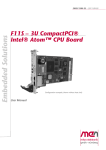
1
Embedded Solutions
20F204-00 E5 – 2012-04-23
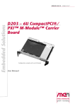
F204/F205 – 3U
CompactPCI® M-Module™
Carrier Board
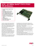
Configuration example (F205)
User Manual
®
F204/F205 - 3U CompactPCI® M-Module™ Carrier Board
F204/F205 - 3U CompactPCI® M-Module™ Carrier Board
The F204/F205 is a 3U M-Module™ carrier board for universal I/O on the
CompactPCI bus. It allows high flexibility in applications such as data acquisition
or process control.
The F205 is slightly higher than standard 3U format, providing enough space for
two M-Modules™ while staying compatible with CompactPCI® housings through
special guide rails already included in the delivery. F204 can carry one
M-Module™. M-Modules™ are screwed tightly on the board and require no
separately mounted transition panel.
The F204/F205 offers developers instant access to more than 70 different
M-Modules™ for I/O in fields such as process I/O, measurement, instrumentation,
motion control, communication, and development.
Technical Data
M-Module™ Slots
•
•
•
•
F204: One M-Module™ slot
F205: Two M-Module™ slots
Compliant with M-Module™ standard
Characteristics: A08, A24, D08, D16, D32, INTA, TRIGI, TRIGO
Peripheral Connections
• Via front panel
CompactPCI® Bus
• Compliance with CompactPCI® Specification 2.0 R2.1
• Only one slot required on the 3U CompactPCI® bus
• 32-bit/33-MHz PCI-to-M-Module™ bridge
- FPGA-based
- Compliant with PCI Specification 2.2
- Target on PCI bus
• V(I/O): +3.3 V (+5 V tolerant)
Electrical Specifications
• Supply voltage/power consumption:
- +5 V (-3%/+5%), 20 mA typ.
- +3.3 V (-3%/+5%), 20 mA typ.
• MTBF: 1 046 000 h @ 50°C (derived from MIL-HDBK-217F)
MEN Mikro Elektronik GmbH
20F204-00 E5 – 2012-04-23
2
Technical Data
Mechanical Specifications
• F204:
- Dimensions: conforming to CompactPCI® specification for 3U boards
- Front panel: aluminum with 1 handle, cut-out for front connector of M-Module™
- Weight: 130 g (without M-Modules™)
• F205:
- Dimensions: 111.7 mm x 160 mm standard
- Front panel: aluminum without handles, cut-outs for front connectors of 2 MModules™
- Weight: 125 g (without M-Modules™)
Environmental Specifications
• Temperature range (operation):
- 0..+60°C or -40..+85°C
- Airflow: min. 10m³/h
• Temperature range (storage): -40..+85°C
• Relative humidity (operation): max. 95% non-condensing
• Relative humidity (storage): max. 95% non-condensing
• Altitude: -300 m to + 3 000 m
• Shock: 15 g, 11 ms
• Bump: 10 g, 16 ms
• Vibration (sinusoidal): 2 g, 10..150 Hz
• Conformal coating on request
Safety
• PCB manufactured with a flammability rating of 94V-0 by UL recognized manufacturers
EMC
• Tested according to EN 55022 (radio disturbance), IEC61000-4-2 (ESD) and
IEC61000-4-4 (burst)
Software Support
• M-Module™ drivers for Windows®, VxWorks®, Linux, QNX®, OS-9® as supported
MEN Mikro Elektronik GmbH
20F204-00 E5 – 2012-04-23
3
Block Diagram
Block Diagram
F
M‐Module
PXI
F
CompactPCI Bus
FPGA
PXI Trigger Lines
M‐Module Interface/
PCI‐to‐Local‐Bus Bridge
M‐Module
(F205)
MEN Mikro Elektronik GmbH
20F204-00 E5 – 2012-04-23
4
Configuration Options
Configuration Options
M-Module™ Slots
• 1 or 2
M-Module™ Characteristics
• A08/D16 or A24/D32 support
Operation Temperature
• 0..+60°C
• -40..+85°C
Cooling Concept
• Also available with conduction cooling in MEN CCA frame
Please note that some of these options may only be available for large volumes.
Please ask our sales staff for more information.
For available standard configurations see online data sheet.
MEN Mikro Elektronik GmbH
20F204-00 E5 – 2012-04-23
5
Product Safety
Product Safety
!
Electrostatic Discharge (ESD)
Computer boards and components contain electrostatic sensitive devices.
Electrostatic discharge (ESD) can damage components. To protect the board and
other components against damage from static electricity, you should follow some
precautions whenever you work on your computer.
• Power down and unplug your computer system when working on the inside.
• Hold components by the edges and try not to touch the IC chips, leads, or circuitry.
• Use a grounded wrist strap before handling computer components.
• Place components on a grounded antistatic pad or on the bag that came with the
component whenever the components are separated from the system.
• Store the board only in its original ESD-protected packaging. Retain the original
packaging in case you need to return the board to MEN for repair.
MEN Mikro Elektronik GmbH
20F204-00 E5 – 2012-04-23
6
About this Document
About this Document
This user manual is intended only for system developers and integrators, it is not intended for end users.
It describes the hardware functions of the board, connection of peripheral devices
and integration into a system. It also provides additional information for special
applications and configurations of the board.
The manual does not include detailed information on individual components (data
sheets etc.). A list of literature is given in the appendix.
History
Issue
Comments
Date
E1
First edition
2003-12-19
E2
General update, minor errors corrected
2006-01-13
E3
New board versions with A24/D32 support
2006-10-27
E4
Corrected CompactPCI I/O voltage, cosmetics
2012-04-20
E5
Corrected CompactPCI I/O voltage in Chapter 3.3
2012-04-23
Conventions
!
italics
bold
monospace
This sign marks important notes or warnings concerning proper functionality of the
product described in this document. You should read them in any case.
Folder, file and function names are printed in italics.
Bold type is used for emphasis.
A monospaced font type is used for hexadecimal numbers, listings, C function
descriptions or wherever appropriate. Hexadecimal numbers are preceded by "0x".
comment
Comments embedded into coding examples are shown in green color.
hyperlink
Hyperlinks are printed in blue color.
The globe will show you where hyperlinks lead directly to the Internet, so you can
look for the latest information online.
IRQ#
/IRQ
Signal names followed by "#" or preceded by a slash ("/") indicate that this signal is
either active low or that it becomes active at a falling edge.
in/out
Signal directions in signal mnemonics tables generally refer to the corresponding
board or component, "in" meaning "to the board or component", "out" meaning
"coming from it".
Vertical lines on the outer margin signal technical changes to the previous issue of
the document.
MEN Mikro Elektronik GmbH
20F204-00 E5 – 2012-04-23
7
About this Document
Legal Information
Changes
MEN Mikro Elektronik GmbH ("MEN") reserves the right to make changes without further notice to any products
herein.
Warranty, Guarantee, Liability
MEN makes no warranty, representation or guarantee of any kind regarding the suitability of its products for any
particular purpose, nor does MEN assume any liability arising out of the application or use of any product or
circuit, and specifically disclaims any and all liability, including, without limitation, consequential or incidental
damages. TO THE EXTENT APPLICABLE, SPECIFICALLY EXCLUDED ARE ANY IMPLIED
WARRANTIES ARISING BY OPERATION OF LAW, CUSTOM OR USAGE, INCLUDING WITHOUT
LIMITATION, THE IMPLIED WARRANTIES OF MERCHANTABILITY AND FITNESS FOR A
PARTICULAR PURPOSE OR USE. In no event shall MEN be liable for more than the contract price for the
products in question. If buyer does not notify MEN in writing within the foregoing warranty period, MEN shall
have no liability or obligation to buyer hereunder.
The publication is provided on the terms and understanding that:
1. MEN is not responsible for the results of any actions taken on the basis of information in the publication, nor
for any error in or omission from the publication; and
2. MEN is not engaged in rendering technical or other advice or services.
MEN expressly disclaims all and any liability and responsibility to any person, whether a reader of the publication
or not, in respect of anything, and of the consequences of anything, done or omitted to be done by any such person
in reliance, whether wholly or partially, on the whole or any part of the contents of the publication.
Conditions for Use, Field of Application
The correct function of MEN products in mission-critical and life-critical applications is limited to the
environmental specification given for each product in the technical user manual. The correct function of MEN
products under extended environmental conditions is limited to the individual requirement specification and
subsequent validation documents for each product for the applicable use case and has to be agreed upon in writing
by MEN and the customer. Should the customer purchase or use MEN products for any unintended or
unauthorized application, the customer shall indemnify and hold MEN and its officers, employees, subsidiaries,
affiliates, and distributors harmless against all claims, costs, damages, and expenses, and reasonable attorney fees
arising out of, directly or indirectly, any claim or personal injury or death associated with such unintended or
unauthorized use, even if such claim alleges that MEN was negligent regarding the design or manufacture of the
part. In no case is MEN liable for the correct function of the technical installation where MEN products are a part
of.
Trademarks
All products or services mentioned in this publication are identified by the trademarks, service marks, or product
names as designated by the companies which market those products. The trademarks and registered trademarks
are held by the companies producing them. Inquiries concerning such trademarks should be made directly to those
companies.
Conformity
MEN products are no ready-made products for end users. They are tested according to the standards given in the
Technical Data and thus enable you to achieve certification of the product according to the standards applicable in
your field of application.
MEN Mikro Elektronik GmbH
20F204-00 E5 – 2012-04-23
8
About this Document
RoHS
Since July 1, 2006 all MEN standard products comply with RoHS legislation.
Since January 2005 the SMD and manual soldering processes at MEN have already been completely lead-free.
Between June 2004 and June 30, 2006 MEN’s selected component suppliers have changed delivery to RoHScompliant parts. During this period any change and status was traceable through the MEN ERP system and the
boards gradually became RoHS-compliant.
WEEE Application
The WEEE directive does not apply to fixed industrial plants and tools. The compliance is the responsibility of the
company which puts the product on the market, as defined in the directive; components and sub-assemblies are
not subject to product compliance.
In other words: Since MEN does not deliver ready-made products to end users, the WEEE directive is not
applicable for MEN. Users are nevertheless recommended to properly recycle all electronic boards which have
passed their life cycle.
Nevertheless, MEN is registered as a manufacturer in Germany. The registration number can be provided on
request.
Copyright © 2012 MEN Mikro Elektronik GmbH. All rights reserved.
Germany
MEN Mikro Elektronik GmbH
Neuwieder Straße 3-7
90411 Nuremberg
Phone +49-911-99 33 5-0
Fax +49-911-99 33 5-901
E-mail [email protected]
www.men.de
MEN Mikro Elektronik GmbH
20F204-00 E5 – 2012-04-23
France
MEN Mikro Elektronik SA
18, rue René Cassin
ZA de la Châtelaine
74240 Gaillard
Phone +33 (0) 450-955-312
Fax +33 (0) 450-955-211
E-mail [email protected]
www.men-france.fr
USA
MEN Micro, Inc.
24 North Main Street
Ambler, PA 19002
Phone (215) 542-9575
Fax (215) 542-9577
E-mail [email protected]
www.menmicro.com
9
Contents
Contents
1 Getting Started . . . . . . . . . . . . . . . . . . . . . . . . . . . . . . . . . . . . . . . . . . . . . . . .
1.1 Map of the Board. . . . . . . . . . . . . . . . . . . . . . . . . . . . . . . . . . . . . . . . .
1.2 Integrating the Board into a System . . . . . . . . . . . . . . . . . . . . . . . . . .
1.3 Installing M-Modules . . . . . . . . . . . . . . . . . . . . . . . . . . . . . . . . . . . . .
1.4 Installing Driver Software . . . . . . . . . . . . . . . . . . . . . . . . . . . . . . . . . .
13
13
14
15
15
2 Connecting the Board . . . . . . . . . . . . . . . . . . . . . . . . . . . . . . . . . . . . . . . . . . . 16
2.1 M-Module Connectors. . . . . . . . . . . . . . . . . . . . . . . . . . . . . . . . . . . . . 16
2.2 PXI Trigger Lines . . . . . . . . . . . . . . . . . . . . . . . . . . . . . . . . . . . . . . . . 17
3 Functional Description . . . . . . . . . . . . . . . . . . . . . . . . . . . . . . . . . . . . . . . . . .
3.1 Power Supply. . . . . . . . . . . . . . . . . . . . . . . . . . . . . . . . . . . . . . . . . . . .
3.2 Identifying the Board. . . . . . . . . . . . . . . . . . . . . . . . . . . . . . . . . . . . . .
3.3 CompactPCI Interface . . . . . . . . . . . . . . . . . . . . . . . . . . . . . . . . . . . . .
3.3.1
Delayed Transactions . . . . . . . . . . . . . . . . . . . . . . . . . . . . . .
3.4 M-Module Interfaces . . . . . . . . . . . . . . . . . . . . . . . . . . . . . . . . . . . . . .
3.4.1
Configuring the M-Module Interfaces . . . . . . . . . . . . . . . . .
3.5 Using Triggers . . . . . . . . . . . . . . . . . . . . . . . . . . . . . . . . . . . . . . . . . . .
18
18
18
19
19
20
20
21
4 Organization of the Board . . . . . . . . . . . . . . . . . . . . . . . . . . . . . . . . . . . . . . .
4.1 PCI Configuration Registers . . . . . . . . . . . . . . . . . . . . . . . . . . . . . . . .
4.1.1
Address Map . . . . . . . . . . . . . . . . . . . . . . . . . . . . . . . . . . . . .
4.2 M-Module Slot Address Spaces . . . . . . . . . . . . . . . . . . . . . . . . . . . . .
24
24
24
25
5 Appendix . . . . . . . . . . . . . . . . . . . . . . . . . . . . . . . . . . . . . . . . . . . . . . . . . . . . . 27
5.1 Literature and Web Resources . . . . . . . . . . . . . . . . . . . . . . . . . . . . . . . 27
5.2 Finding out the Product’s Article Number, Revision and
Serial Number . . . . . . . . . . . . . . . . . . . . . . . . . . . . . . . . . . . . . . . . . . . 27
MEN Mikro Elektronik GmbH
20F204-00 E5 – 2012-04-23
10
Figures
Figure 1.
Figure 2.
Figure 3.
Figure 4.
Figure 5.
Figure 6.
MEN Mikro Elektronik GmbH
20F204-00 E5 – 2012-04-23
Map of the board – F204 – top view . . . . . . . . . . . . . . . . . . . . . . . . . .
Map of the board – F205 – top view . . . . . . . . . . . . . . . . . . . . . . . . . .
Installing an M-Module . . . . . . . . . . . . . . . . . . . . . . . . . . . . . . . . . . . .
Trigger routing . . . . . . . . . . . . . . . . . . . . . . . . . . . . . . . . . . . . . . . . . . .
Trigger routing – examples. . . . . . . . . . . . . . . . . . . . . . . . . . . . . . . . . .
Labels giving the product’s article number, revision and
serial number . . . . . . . . . . . . . . . . . . . . . . . . . . . . . . . . . . . . . . . . . . . .
13
14
15
21
22
27
11
Tables
Table 1.
Table 2.
Table 3.
Table 4.
Table 5.
Table 6.
MEN Mikro Elektronik GmbH
20F204-00 E5 – 2012-04-23
Pin assignment of the 60-pin plug connectors . . . . . . . . . . . . . . . . . . .
Signal mnemonics of the M-Module connector . . . . . . . . . . . . . . . . . .
PXI trigger lines on CompactPCI J2 (110-pin type "B" modified) . . .
PCI configuration registers. . . . . . . . . . . . . . . . . . . . . . . . . . . . . . . . . .
M-Module address map for board versions with A08/D16 support. . .
M-Module address map for board versions with A24/D32 support. . .
16
17
17
24
25
26
12
Getting Started
1
Getting Started
This chapter will give an overview of the carrier board and some hints for first
installation in a system as a "check list".
1.1
Map of the Board
Figure 1. Map of the board – F204 – top view
MEN Mikro Elektronik GmbH
20F204-00 E5 – 2012-04-23
Holes for M-Module
mounting screws
M-Module 0
60-pin M-Module
bus connector
CompactPCI Connector J1
Front-panel
mounting screws
(accessible from
solder side of
board)
CompactPCI Connector J2
F204
13
Getting Started
Figure 2. Map of the board – F205 – top view
M-Module 1
60-pin M-Module
bus connector
Holes for M-Module
mounting screws
M-Module 0
60-pin M-Module
bus connector
Front-panel
mounting screws
(accessible from
solder side of
board)
1.2
CompactPCI Connector J1
Holes for M-Module
mounting screws
CompactPCI Connector J2
F205
Integrating the Board into a System
You can use the following "check list" when installing the F204 in a CompactPCI
system for the first time.
!
Note: The F204 must not be inserted into the system slot! The system slot of every
CompactPCI system is marked by a
triangle on the backplane and/or at the
front panel.
Power-down the system.
Install an M-Module on the F204 as described in Chapter 1.3 Installing M-Modules on page 15.
Insert the F204 into your CompactPCI system, making sure that the CompactPCI connectors are properly aligned.
Power-up the system.
You can now install driver software for the F204 and M-Modules.
MEN Mikro Elektronik GmbH
20F204-00 E5 – 2012-04-23
14
Getting Started
1.3
Installing M-Modules
Perform the following steps to install an M-Module:
Loosen the front-panel mounting screws at the solder side of the board and
remove the whole front panel (two screws with F204, four screws with F205)
(see Figure 1, Map of the board – F204 – top view, on page 13 and Figure 2,
Map of the board – F205 – top view, on page 14).
Hold the M-Module over the target slot of the carrier board with the component
sides facing each other.
Align the 60-pin connectors of the M-Module and carrier board.
Press the M-Module carefully but firmly on the F204, making sure that the connectors are properly linked.
Turn the F204 upside down and use four M-Module mounting screws to fasten
the M-Module on the solder side of the F204.
Re-install the front panel of the F204.
!
Note: You can order suitable mounting screws from MEN, see MEN’s website. In
any case, use only the screw types specified in the following figure!
!
Note: Older M-Modules with a solder side cover may collide with the front panel. If
you have any problems, please contact MEN’s technical support:
[email protected].
Figure 3. Installing an M-Module
M-Module
Mounting Bolt
60-pin connector
Carrier board without front panel
M3x6 cross-recess pan-head screws
(F204)
M3x6 cross-recess countersink-head
screws removed before (F205)
1.4
M3x6 slotted panhead screws
(plastics)
Installing Driver Software
For a detailed description on how to install driver software please refer to the
respective documentation.
You can find any driver software available for download on MEN’s website.
MEN Mikro Elektronik GmbH
20F204-00 E5 – 2012-04-23
15
Connecting the Board
2
Connecting the Board
2.1
M-Module Connectors
Connector types:
• Three 20-pin plugs, 2.54mm pitch, square pins 0.635mm gold
• Mating connector:
Three 20-pin receptacles, high-precision, 2.54mm pitch, for square pins
0.635mm gold, 6.9mm height
Note: Signals which are not bussed (i.e. which are applied to each M-Module slot
independently) are indexed with "x". For each slot, replace "x" with the slot
number (0..3).
Table 1. Pin assignment of the 60-pin plug connectors
A B C
1
20
A
B
C
1
/CSx
GND
/AS
2
A01
+5V
D16
3
A02
+12V
D17
4
A03
-12V
D18
5
A04
GND
D19
6
A05
/DREQx
D20
7
A06
/DACKx
D21
8
A07
GND
D22
9
D08/A16
D00/A08
TRIGA
10
D09/A17
D01/A09
TRIGB
11
D10/A18
D02/A10
D23
12
D11/A19
D03/A11
D24
13
D12/A20
D04/A12
D25
14
D13/A21
D05/A13
D26
15
D14/A22
D06/A14
D27
16
D15/A23
D07/A15
D28
17
/DS1
/DS0
D29
18
/DTACKx
/WRITE
D30
19
/IACKx
/IRQx
D31
20
/RESET
SYSCLKx
/DS2
Due to the characteristics, the following pins are not supported on the carrier board:
• /DREQx
• /DACKx
MEN Mikro Elektronik GmbH
20F204-00 E5 – 2012-04-23
16
Connecting the Board
Note: There are different board versions with A08/D16 or A24/D32 M-Module support. If you are not sure which type of addressing your carrier board supports,
you can check the different models on MEN’s website.
Table 2. Signal mnemonics of the M-Module connector
Name
!
Direction
Function
D00/A08..D15/A23
in/out
Multiplexed data/address bus
D16..D31
in/out
Most significant portion of data bus
A01..A07
out
Address bus
/WRITE
out
Read/write enable
/CS
out
M-Module chip select
/DTACK
in
Data acknowledge
/DS0..1
out
Data bus select signals
/RESET
out
M-Module reset
/IRQ
in
Interrupt request
/IACK
out
Interrupt acknowledge
/DREQ
in
DMA request (not supported)
/DACK
out
DMA acknowledge (not supported)
SYSCLK
out
16-MHz clock
GND
-
Logical reference signal
+5V, +12V, -12V
out
Power supplies
/AS
out
Address strobe for multiplexed address/data
bus
TRIGA, TRIGB
in/out
Trigger inputs/outputs
Note: The 24-pin receptacle connector of M-Module slot 0 is provided only for
mechanical stability. The I/O signals from the M-Module at this connector are
not used.
2.2
PXI Trigger Lines
The carrier board supports PXI trigger lines PXI_TRIG[7:0]. These are located on
CompactPCI J2 as shown below:
Table 3. PXI trigger lines on CompactPCI J2 (110-pin type "B" modified)
F EDCB A
18
17
16
MEN Mikro Elektronik GmbH
20F204-00 E5 – 2012-04-23
F
E
D
C
18
GND
PXI_TRIG6
GND
17
GND
-
-
-
16
GND
PXI_TRIG7
-
-
B
A
PXI_TRIG5 PXI_TRIG4 PXI_TRIG3
GND
PXI_TRIG2
PXI_TRIG0 PXI_TRIG1
17
Functional Description
3
Functional Description
3.1
Power Supply
Power supply is fed via the CompactPCI backplane. The board operates on +5V and
+3.3V. +12V/-12V may be required by one of the M-Modules installed. Power
consumption is 20 mA typ. plus the current drawn by M-Modules stacked on the
carrier board.
3.2
Identifying the Board
You can identify the carrier board as follows:
Note: MEN drivers will also identify the board in this way.
Scan all PCI buses in the system for
- the vendor ID: 0x1172, and
- the FPGA’s device ID:
0xD203 with A08 M-Module access boards, or
0x203D with A24 M-Module access boards.
Note:There are different board versions for A08 or A24 M-Module addressing.
If you are not sure which type of addressing your carrier board supports,
you can check the different models on MEN’s website.
Check if the Subsystem Vendor ID is set to 0xFF00 and the Subsystem ID is set
to 0xFF00 in the PCI config state (see Table 4, PCI configuration registers, on
page 24).
MEN Mikro Elektronik GmbH
20F204-00 E5 – 2012-04-23
18
Functional Description
3.3
CompactPCI Interface
The F204 carrier board has a 32-bit CompactPCI interface on connectors J1/J2. It
uses a 3.3 V signaling voltage on CompactPCI. For a pinout of the 32-bit
CompactPCI interface on J1/J2 and a general description of CompactPCI, please
refer to the CompactPCI specification.
Connector types of J1/J2:
• 110-pin shielded, 2mm-pitch, 5-row receptacle according to IEC 917 and IEC
1076-4-101
The interface is implemented using an FPGA and is compliant to the PCI
Specification Rev. 2.2.
3.3.1
Delayed Transactions
The F204 supports delayed transactions across the CompactPCI bus, i.e. if the F204
cannot deliver (on a read cycle) or accept (for a write cycle) data within 16 PCI
clock cycles, it responds to the current bus master with a retry. In response to the
retry, the bus master relinquishes the CompactPCI bus, which can now be used by
another bus master. In the meantime, the F204 processes the retried transaction on
the M-Module interface. When the bus master retries the bus cycle on PCI, the F204
will terminate the cycle with zero wait states. This will improve overall system
throughput. Even slow M-Modules do not tie up the whole CompactPCI bus.
MEN Mikro Elektronik GmbH
20F204-00 E5 – 2012-04-23
19
Functional Description
3.4
M-Module Interfaces
The M-Module interfaces of the F204 comply with the M-Module specification.
They support the following M-Module characteristics: D08, D16, D32, A08, A24,
INTA, TRIGI, TRIGO. It depends on the board version whether the F204 supports
A08/D16 or A24/D32 accesses.
If you are not sure which type of addressing your carrier board supports, you can
check the different models on MEN’s website.
The F204 does not support burst mode, since this leads to conflicts with the PCI
architecture.
3.4.1
Configuring the M-Module Interfaces
M-Module Control/Status Register (read/write)
31..18
17
GIEN GIRQ
-
GIEN
GIRQ
TOUT
PCIRET
IEN
IRQ
MEN Mikro Elektronik GmbH
20F204-00 E5 – 2012-04-23
16
15..4
3
2
1
0
-
TOUT
PCI
RET
IEN
IRQ
Global interrupt enable bit (common to all M-Modules)
0 = Disable interrupt
1 = Enable interrupt
Global interrupt pending (common to all M-Modules) (read-only)
1 = Interrupt pending
Timeout
1 = Timeout occurred. Write 1 to clear.
PCI retries
0 = PCI retries during access (slower)
1 = No PCI retries during access (faster) (default)
You should change this setting to 0 ("slower") if you can expect the
M-Module access to be slower than 450 ns. Otherwise, leave the default
setting as is.
Interrupt enable bit
0 = Disable interrupt
1 = Enable interrupt
Interrupt pending (read-only)
1 = Interrupt pending
20
Functional Description
3.5
Using Triggers
There are 8 internal trigger lines, the "internal trigger bus". Every PXI trigger line
can drive one and can be driven by one dedicated internal trigger line. This is set in
the PXI Trigger Source and Destination Registers for each M-Module.
Every M-Module trigger line (TRIGA/TRIGB) can be driven by and can drive every
internal trigger line. If there is more than one source for an internal trigger, all
connected sources are ORed.
There is one Trigger Source Register and one Trigger Destination Register per
M-Module. Bits 31..16 of the Trigger Source and Trigger Destination Registers are
global, i.e. the PXI trigger lines can only be accessed for all M-Modules together.
The maximum propagation delay between a trigger source and trigger destination
amounts to 25 ns.
Figure 4. Trigger routing
PXI Trigger Lines
Bits 23..16
Internal Trigger Bus
7 6 5 4 3 2 1 0
PXI Source
7 6 5 4 3 2 1 0
PXI Destination
M-Module 0
Bits 15..8
TRIGB Source
7 6 5 4 3 2 1 0
TRIGB Destination
TRIGA Destination
7 6 5 4 3 2 1 0
TRIGA Source
Bits 7..0
M-Module 1
MEN Mikro Elektronik GmbH
20F204-00 E5 – 2012-04-23
21
Functional Description
Figure 5. Trigger routing – examples
PXI Trigger Lines
Bits 23..16
Internal Trigger Bus
7 6 5 4 3 2 1 0
0 0 0 0 1 0 0 0 PXI Source
7 6 5 4 3 2 1 0
0 0 1 0 0 0 0 0 PXI Destination
M-Module 0
Bits 15..8
TRIGB Source 0 0 1 0 0 0 0 0
7 6 5 4 3 2 1 0
TRIGB Destination 0 0 0 0 0 0 0 0
TRIGA Destination 0 0 0 0 1 0 0 0
7 6 5 4 3 2 1 0
TRIGA Source 0 0 0 0 0 0 0 0
Bits 7..0
M-Module 1
MEN Mikro Elektronik GmbH
20F204-00 E5 – 2012-04-23
22
Functional Description
Trigger Source Register (read/write)
31..24
23..16
-
PXI Source 7..0
15..8
7..0
M-Module Source TRIGB 7..0
M-Module Source TRIGA 7..0
PXI Source
M-Module Source TRIGB
M-Module Source TRIGA
1 = The corresponding PXI input is connected to
internal trigger line 7..0. (Common to all
M-Modules)
1 = Trigger input TRIGB of the addressed
M-Module is connected to the corresponding
internal trigger line 7..0.
1 = Trigger input TRIGA of the addressed
M-Module is connected to the corresponding
internal trigger line 7..0.
Trigger Destination Register (read/write)
31..24
23..16
-
PXI Destination 7..0
15..8
7..0
M-Module Destination TRIGB 7..0
M-Module Destination TRIGA 7..0
PXI Destination
1 = The corresponding internal trigger line is
connected to PXI trigger line 7..0. This line
becomes an output and no longer an input line.
(Common to all M-Modules)
M-Module Destination TRIGB 1 = The corresponding internal trigger line is
connected to TRIGB of the addressed
M-Module. This TRIGB line becomes an output
and no longer an input line.
M-Module Destination TRIGA 1 = The corresponding internal trigger line is
connected to TRIGA of the addressed
M-Module. This TRIGA line becomes an output
and no longer an input line.
Note: It is not forbidden but may make no sense to activate a trigger line as an output and use this line as an input as well. Care shall be taken to prevent loops!
Using PXI 0 as an input connected to internal line 0, and activating PXI as an
output as well might cause heavy oscillation or any other non-deterministic
behavior.
MEN Mikro Elektronik GmbH
20F204-00 E5 – 2012-04-23
23
Organization of the Board
4
Organization of the Board
The F204 complies with PCI specification 2.2. All resources requested by the F204
are mapped through the PCI configuration space. For a detailed description of the
PCI configuration space, please refer to the PCI specification.
4.1
PCI Configuration Registers
4.1.1
Address Map
The following register map is shown for reference only.
Table 4. PCI configuration registers
Address
D31..D24
D23..D16
D15..D8
D7..D0
R/W
0x00
Device ID (A08: 0xD203 / A24: 0x203D)1
Vendor ID (0x1172)
R
0x04
Status (0x0400)
Command (0x0007)
R/W
0x08
Class Code (0x068000)
0x0C
BIST (0x00)
0x10
PCI Base Address 0 for Memory Mapped FPGA Registers
R/W
0x14
PCI Base Address 1 — Not used
R/W
0x18
PCI Base Address 2 — Not used
R/W
0x1C
PCI Base Address 3 — Not used
R/W
0x20
PCI Base Address 4 — Not used
R/W
0x24
PCI Base Address 5 — Not used
R/W
0x28
CardBus CIS Pointer (0x00000000)
R
0x2C
Subsystem ID (0xFF00)
0x30
Expansion ROM Register (0x00000000)
R/W
0x34
Reserved (0x00000000)
R
0x38
Reserved (0x00000000)
R
0x3C
Max_Lat (0x00)
1
Header Type
(0x00)
Min_Gnt (0x00)
Latency Timer
(0x40)
Revision ID
R
Cache Line Size
R/W
Subsystem Vendor ID (0xFF00)
Interrupt Pin
(0x01)
Interrupt Line
R
R/W
There are different board versions for A08 or A24 M-Module addressing. If you are not sure which type of addressing your carrier board supports, you can check the different models on MEN’s website.
MEN Mikro Elektronik GmbH
20F204-00 E5 – 2012-04-23
24
Organization of the Board
4.2
M-Module Slot Address Spaces
Each M-Module slot is provided with a 1-KB address space with A08 access or a
32-MB address space with A24 access. (See also Chapter 3.4 M-Module Interfaces
on page 20.) The base address within the PCI address space is set by the
corresponding base address registers in the PCI configuration space. Each of the MModule address spaces is divided into three distinct areas:
• An area for A24 access cycles (depending on the board version).
• An area for A08 access cycles.
• An area for accesses to additional control registers.
Table 5. M-Module address map for board versions with A08/D16 support
M-Module
M-Module 0
M-Module 1
(only F205)
MEN Mikro Elektronik GmbH
20F204-00 E5 – 2012-04-23
Offset Address Range
Function
0x0000..0x00FF
Reserved
0x0100..0x01FF
Reserved
0x0200..0x02FF
A08/D16 access
0x0300..0x0303
A08/D16 IACK
0x0304..0x0307
Control/Status Register
0x0308..0x030B
Trigger Source Register
0x030C..0x030F
Trigger Destination Register
0x0400..0x04FF
Reserved
0x0500..0x05FF
Reserved
0x0600..0x06FF
A08/D16 access
0x0700..0x0703
A08/D16 IACK
0x0704..0x0707
Control/Status Register
0x0708..0x070B
Trigger Source Register
0x070C..0x070F
Trigger Destination Register
25
Organization of the Board
Table 6. M-Module address map for board versions with A24/D32 support
M-Module
M-Module 0
M-Module 1
(only F205)
MEN Mikro Elektronik GmbH
20F204-00 E5 – 2012-04-23
Offset Address Range
Function
0x000 0000..0x0FF FFFF
A24/D32 access
0x100 0000..0x1FF FCFF
A24/D16 access
0x1FF FD00..0x1FF FDFF
A08/D32 access
0x1FF FE00..0x1FF FEFF
A08/D16 access
0x1FF FF00..0x1FF FF03
A08/D16 IACK
0x1FF FF04..0x1FF FF07
Control/Status Register
0x1FF FF08..0x1FF FF0B
Trigger Source Register
0x1FF FF0C..0x1FF FF0F
Trigger Destination Register
0x200 0000..0x2FF FFFF
A24/D32 access
0x300 0000..0x3FF FCFF
A24/D16 access
0x3FF FD00..0x3FF FDFF
A08/D32 access
0x3FF FE00..0x3FF FEFF
A08/D16 access
0x3FF FF00..0x3FF FF03
A08/D16 IACK
0x3FF FF04..0x3FF FF07
Control/Status Register
0x3FF FF08..0x3FF FF0B
Trigger Source Register
0x3FF FF0C..0x3FF FF0F
Trigger Destination Register
26
Appendix
5
Appendix
5.1
Literature and Web Resources
• F204 data sheet with up-to-date information and documentation:
www.men.de
• F205 data sheet with up-to-date information and documentation:
www.men.de
• M-Module Standard:
ANSI/VITA 12-1996, M-Module Specification;
VMEbus International Trade Association
www.vita.com
• CompactPCI Specification Revision 2.0 R2.1:
1997; PCI Industrial Computers Manufacturers Group (PICMG)
www.picmg.org
5.2
Finding out the Product’s Article Number, Revision and
Serial Number
MEN user documentation may describe several different models and/or design
revisions of the F204. You can find information on the article number, the design
revision and the serial number on a label attached to the board.
• Article number: Gives the product’s family and model. This is also MEN’s
ordering number. To be complete it must have 9 characters.
• Revision number: Gives the design revision of the product.
• Serial number: Unique identification assigned during production.
If you need support, you should communicate these numbers to MEN.
Figure 6. Labels giving the product’s article number, revision and serial number
Made in
Germany
Article No.:
02F205-00
Rev.No.:
00.00.00
Complete article number Revision number
MEN Mikro Elektronik GmbH
20F204-00 E5 – 2012-04-23
Serial number
27