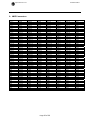
1
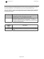
HYTEC ELECTRONICS Ltd
HEAD OFFICE: 5 CRADOCK ROAD, READING, BERKS. RG2 0JT, UK
Telephone: +44 (0) 118 9757770
Fax: +44 (0)118 9757566
E-mail: [email protected]
DIO8005 VME64x
128Bit TTL DIGITAL I/O BOARD
(Optical Isolation optional through rear mounted transition board)
USERS MANUAL
Document Nos.: DIO-8005/UTM/1.1
Date: 12/12/2007
Author: AB/MCB/DAN
Hytec Electronics Ltd
DIO8005/UTM/1.1
CONTENTS
1.
PRODUCT DESCRIPTION ..........................................................................................................................3
1.1
2.
KEY FEATURES .......................................................................................................................................5
USE OF THE VME DATA BUS AND MEMORY ACCESS .........................................................................6
2.1
VME ADDRESSING ..................................................................................................................................6
2.1.1
Short Addressing (A16 AM29h and 2Dh) .....................................................................................6
2.1.2
Standard Addressing (A24 AM39h and 3Dh) ...............................................................................7
2.1.3
Configuration ROM (A24 AM2Fh) ................................................................................................7
3.
REGISTERS .................................................................................................................................................8
3.1
LAST KNOWN CHANGE REGISTER (READ/WRITE) .....................................................................................9
3.2
CONTROL/STATUS REGISTER DIGITAL IO (CSR IO) (READ/WRITE) ..........................................................9
3.3
DIGITAL INPUT INTERRUPT MASK REGISTER IMR (READ/WRITE) ............................................................10
3.4
DE-BOUNCE BIT REGISTER (READ/WRITE) ............................................................................................10
3.5
PULSE SELECT REGISTER PSR IP (READ/WRITE) .................................................................................11
3.6
PULSE PARAMETER REGISTER PPR IP (READ/WRITE) ...........................................................................11
3.7
FIFO REGISTER FIFO IP (READ/WRITE) ...............................................................................................12
3.7.1
Example of FIFO contents ..........................................................................................................12
3.8
FIFO MEMORY (READ)..........................................................................................................................13
3.9
INTERRUPT REQUEST VECTOR IRV IP (READ/WRITE).............................................................................14
3.10 CONTROL & STATUS REGISTER (VME) ..................................................................................................14
3.11 VME SYSTEM RESET ............................................................................................................................15
4.
INTERRUPT PROCESS ............................................................................................................................16
5.
CONFIGURATION ROM............................................................................................................................17
5.1
BOARD SERIAL NO. ...............................................................................................................................17
5.2
OTHER JUMPER SETTINGS ....................................................................................................................18
5.2.1
LI/I*, LI/O* Jumper Settings ........................................................................................................18
6.
ID PROM REGISTERS (GREEN SPRING FORMAT)...............................................................................18
7.
PRODUCT SPECIFICATIONS...................................................................................................................19
8.
VME CONNECTORS .................................................................................................................................20
9.
EXAMPLE CODE .......................................................................................................................................21
9.1
QUICK ADDRESSING TEST .....................................................................................................................21
9.2
SIMPLE DIGITAL INPUT READING. ...........................................................................................................22
Set Up.........................................................................................................................................................22
9.3
SIMPLE DIGITAL OUTPUT DRIVING..........................................................................................................22
Set Up.........................................................................................................................................................22
9.4
READING THE FIFO...............................................................................................................................23
Set Up.........................................................................................................................................................23
Reading Input Values from the FIFO..........................................................................................................23
9.5
INTERRUPTS. ........................................................................................................................................24
Set Up.........................................................................................................................................................24
10.
10.1
EPICS DRIVER ......................................................................................................................................25
INTRODUCTION ......................................................................................................................................25
Page 2 of 26
Hytec Electronics Ltd
DIO8005/UTM/1.1
1. PRODUCT DESCRIPTION
The DIO 8005 is a 6U (double height) VME64x digital I/O board constructed to the VME64x
standard. It provides 128 TTL digital I/O bits organised in four groups of 32 bits each with an input
and an output strobe. Each group of 32 bits may be programmed to act as inputs or outputs.
For users familiar with the Hytec 8505 Industry Pack (IP) Card, the 8005 can be considered as 8 x
8505 on a single carrier card, but with the following restrictions…
1. Each block of 32 bits (equivalent to 2 x 8505) can ONLY be set up as All Inputs or All
Outputs.
2. Setting parameters such a de-bounce value, scan rate etc also applies to the whole 32 bit
block.
3. ONLY Internal Clock is available, the 8505 external clock or strobe input options are NOT
available.
When a group is in ‘input mode’, the module features change-of-state detection and contact debounce. A small FIFO memory, one for each input group, allows a historical record of the change-ofstate input data to be stored; up to 64 samples. A further register associated with each input group
controls which bits may generate an interrupt. This function has no effect when in output mode.
When a group is in ‘output mode’, outputs may be programmed as levels or pulses of programmed
duration. A pulse parameter register determines the duration of pulsed outputs up to 100 seconds.
All the above registers occupy I/O space on the card in four groups, starting at offset zero+a (where
a = 000hex, 100hex, 200hex or 300hex) as follows:
Offset
a+0
a+4
a+8
a+C
a+10
a+14
a+18
a+1C
a+20
Name
LKC
CSR
IMR
DBR
PSR
PPR
FIFO_R
LKC_FIFO
IRV
Description
Last Known Change/Data Register
Control and Status Register
Mask Register
De-bounce Register
Pulse Select Register
Pulse Parameter Register
FIFO Register
FIFO Memory
Interrupt Request Vector
The module features hot-swap capability with auto power up and host interaction. An on-board
FPGA allows full mapping of the IP board memory, I/O and ID spaces.
The VME interface supports short I/O access A16:D32:D16:D08 (EO), standard I/O access
A24:D64.D32:D16:D08 (EO).
One of VME bus interrupt lines IRQ1 to IRQ7 can be selected and enabled by writing to an on-board
register. The base address of extended memory can be set by register (offset addressing) or by
geographical addressing lines.
Two groups of four front panel mounted LED’s light to visually indicate when a change of state has
been detected and the scan rate on individual groups (A, B, C and D) of 32 bits. See Table in
Section 7 for more details.
There is a TTL ‘Inhibit’ input on the front panel that allows the user to control when data is written to
the FIFO memory.
Page 3 of 26
Hytec Electronics Ltd
DIO8005/UTM/1.1
All I/Os are sampled via the VME backplane P0 and P2 connectors as specified in the VME64
extensions specification. The I/O signals connect via rear mounted transition cards.
Hytec has available a range of rear-mounted transition cards with high-density 50-way [SCSI2]
connectors, which can cater for all I/O signals and provide any necessary signal conditioning,
including optical isolation.
Transition Card
Description
8304
A Straight Through Signal Transition Board, which allows direct
electrical access to TTL Level Signals from the 8005.
A 4-Group (directly relating to 8005’s 32 bit Groups A, B, C and D)
Mixed Signal Transition Board, which accepts up to four 9307 or
9308 signal conditioning boards (see table below). This allows any
set up mix of inputs and outputs on the 8005 to be perfectly matched
to its signal conditioning board.
8308
Signal
Conditioning
Board
9307
9308
Description
This board provides 32 opto-coupled inputs
This board provides 32 opto-coupled high current output MOSFET
drivers.
Page 4 of 26
Hytec Electronics Ltd
DIO8005/UTM/1.1
1.1 Key Features
•
VME64 extensions / Industry Pack Carrier Board
•
VME64x rear panel I/O
•
Full EMC shielding and insertion/extraction handles
•
Fully Hot-Swap capable with auto power-up and host interaction
•
6U (double height) VME base card
•
User selectable VME interrupt level
•
Geographical addressing
•
Front panel TTL Inhibit signals allow control of timing synchronisation
•
VME 64x Configuration ROM
•
On-board 32MHz clock generation
•
VME64x guide pin and slot keying
•
3.3V and 5V supply to P2 connector
Page 5 of 26
Hytec Electronics Ltd
DIO8005/UTM/1.1
2. USE OF THE VME DATA BUS AND MEMORY ACCESS
2.1 VME Addressing
The module uses A16/D32/D16/D08 (EO) (Even and Odd byte3) or A24/D32/D16/D08 (EO) for
accesses to Registers.
The base address of these areas is determined either by PCB jumper settings (J6 to J10) or by
VME64x geographical addressing lines GA0 to GA4.
The PCB jumpers are used only where geographical addressing is not available and will override
the GA lines so they should not be fitted in a GA crate.
Address
I/O Base+
Offset
0x0000
I/O Base +
0x0100
I/O Base +
0x0200
I/O Base+
0x0300
I/O Base+
0x0400
I/O Base+
0x0480
I/O Base+
0x0600
Range
Assignment
0x0000
Registers I/O Bank A I/O 1 to 32
0x001C
0x0100
Registers I/O Bank B I/O 33 to 64
0x011C
0x0200
Registers I/O Bank C I/O 65 to 96
0x021C
0x0300
Registers I/O Bank D I/O 97 to
0x031C
128
0x0400
Carrier on board Registers VME
0x041E
0x0480
Green Springs Type ID
0x04FF
(Not Used/Implemented)
0x0600
VME64x configuration ROM
0x07FF
(See Configuration ROM)
DIO-8005 A16 and A24 address Map
Size
32 Bytes
32 Bytes
32 Bytes
32 Bytes
32 Bytes
128 Bytes
512 Bytes
2.1.1 Short Addressing (A16 AM29h and 2Dh)
In Short address mode the geographical addressing lines equate to the address lines GA0 =A11 to
GA4=A15 and the jumper address setting J6=A11 to J10=A15.
A11 - A15 is the module address determined by the setting of the relevant PCB jumpers or
geographical address lines
Address modifiers
IP I/O, IP ID and Carrier board Configuration Registers:
AM29 Short (A16) non-privileged.
AM2D Short (A16) supervisory.
Page 6 of 26
Hytec Electronics Ltd
DIO8005/UTM/1.1
2.1.2 Standard Addressing (A24 AM39h and 3Dh)
The A24 base address is determined either by PCB jumper settings J6=A19 to J10=A23 or by
geographical addressing lines GA0 =A19 to GA4=A23.
Address modifiers
IP I/O, IP ID and Carrier board Configuration Registers:
AM39 - Standard (A24) non-privileged.
AM3D - Standard (A24) supervisory.
2.1.3 Configuration ROM (A24 AM2Fh)
See Section 5 for the contents of the configuration ROM.
Address modifiers
AM2F - Configuration ROM/Control & Status Registers. Address selection as above
The ROM can be read using A16/A24 addressing with AM codes 29Hex, 2DHex, 39Hex or 3DHex
and 2FHex for CR/CSR space.
Page 7 of 26
Hytec Electronics Ltd
DIO8005/UTM/1.1
3. REGISTERS
The configuration and control of the 8005 module is via registers:
DIO-8005 On-Board Registers
Base
Offset Register
Description
Base +
Base +
Base +
Base +
Base +
0x000
0x004
0x008
0x00C
0x010
Last Known Change/ Data Reg A
Control & Status Register IO A
Mask Register IMR A
De-bounce Bit Register DBR A
Pulse Select Register PSR A
Base +
Base +
0x014
0x018
Base +
Base +
0x01C
0x020
Holds the last known state of inputs in group A, 32Bits
CSR set up of I/O Group A
Selects inputs to mask in group A. 32 bit Register
Selects inputs to de-bounce in group A. 32 bit Register
Selects which outputs will be pulsed outputs in Group
A,32Bits
Pulse Parameter Register PPR A Selects frequency of pulsed outputs in Group A, 32Bits
FIFO Register FIFO_REG A
FIFO control Register for Group A, flag status, FIFO enable &
clear
FIFO Memory FIFO_MEM A
Holds the history of change state values for Group A,
Interrupt Request Vector IRV A
Holds the interrupt vector for Group A
Base +
Base +
Base +
Base +
Base +
0x100
0x104
0x108
0x10C
0x110
Last Known Change/ Data Reg B
Control & Status Register IO B
Mask Register IMR B
De-bounce Bit Register DBR B
Pulse Select Register PSR B
Base +
Base +
0x114
0x118
Base +
Base +
0x11C
0x120
Holds the last known state of inputs in group B, 32Bits
CSR set up of I/O Group B
Selects inputs to mask in group B. 32 bit Register
Selects inputs to de-bounce in group B. 32 bit Register
Selects which outputs will be pulsed outputs in Group
B,32Bits
Pulse Parameter Register PPR B Selects frequency of pulsed outputs in Group B,32Bits
FIFO Register FIFO_REG B
FIFO control Register for Group B, flag status, FIFO enable &
clear
FIFO Memory FIFO_MEM B
Holds the history of change state values for Group B
Interrupt Request Vector IRV B
Holds the interrupt vector for Group B
Base +
Base +
Base +
Base +
Base +
0x200
0x204
0x208
0x20C
0x210
Last Known Change/ Data Reg C
Control & Status Register IO C
Mask Register IMR C
De-bounce Bit Register DBR C
Pulse Select Register PSR C
Base +
Base +
0x214
0x218
Base +
Base +
0x21C
0x220
Holds the last known state of inputs in group C, 32Bits
CSR set up of I/O Group C
Selects inputs to mask in group C. 32 bit Register
Selects inputs to de-bounce in group C. 32 bit Register
Selects which outputs will be pulsed outputs in Group
C,32Bits
Pulse Parameter Register PPR C Selects frequency of pulsed outputs in Group C,32Bits
FIFO Register FIFO_REG C
FIFO control Register for Group C, flag status, FIFO enable &
clear
FIFO Memory FIFO_MEM C
Holds the history of change state values for Group C
Interrupt Request Vector IRV C
Holds the interrupt vector for Group C
Base +
Base +
Base +
Base +
Base +
0x300
0x304
0x308
0x30C
0x310
Last Known Change/ Data Reg D
Control & Status Register IO D
Mask Register IMR D
De-bounce Bit Register DBR D
Pulse Select Register PSR D
Base +
Base +
0x314
0x318
Base +
Base +
0x31C
0x320
Base +
0x400 Control & Status Register
Holds the last known state of inputs in group D, 32Bits
CSR set up of I/O Group D
Selects inputs to mask in group D. 32 bit Register
Selects inputs to de-bounce in group D. 32 bit Register
Selects which outputs will be pulsed outputs in Group
D,32Bits
Pulse Parameter Register PPR D Selects frequency of pulsed outputs in Group D,32Bits
FIFO Register FIFO_REG D
FIFO control Register for Group D, flag status, FIFO enable &
clear
FIFO Memory FIFO_MEM D
Holds the history of change state values for Group D
Interrupt Request Vector IRV D
Holds the interrupt vector for Group D
Set up of VME
Note: The Last Known Change Registers form the 128 bits I/O data
Page 8 of 26
Hytec Electronics Ltd
DIO8005/UTM/1.1
There are 4 groups of 9 application (I/O) registers, each group of 32 I/Os are offset by ‘a’ as follows.
Group A = 0x00Hex offset, Group B = 100Hex offset, Group C = 200Hex offset and Group D =
300Hex offset.
3.1 Last Known Change Register (Read/Write)
Address:
Address:
Address:
Address:
Base + 0x0000 = Group A I/O = 1 to 32
Base + 0x0100 = Group B I/O = 33 to 64
Base + 0x0200 = Group C I/O = 65 to 96
Base + 0x0300 = Group D I/O = 97 to 128
D15 D14 D13 D12 D11 D10 D09 D08 D07 D06 D05 D04 D03 D02 D01 D00
LKC15 LKC14 LKC13 LKC12 LKC11 LKC10 LKC9 LKC8 LKC7 LKC6 LKC5 LKC4 LKC3 LKC2 LKC1 LKC0
D31 D30 D29 D28 D27 D26 D25 D24 D23 D22 D21 D20 D19 D18 D17 D16
LKC31 LKC30 LKC29 LKC28 LKC27 LKC26 LKC25 LKC24 LKC23 LKC22 LKC21 LKC20 LKC19 LKC18 LKC17 LKC16
This register shows the last known state of the I/O data. In the case of inputs it shows the input
states conditioned by de-bounce and change-of-state detection. For outputs, the new data should
be written here.
At switch on the default value is 0Hex
3.2 Control/Status Register Digital IO (CSR IO) (Read/Write)
Address:
Address:
Address:
Address:
Base + 0x0004 = Group A I/O = 1 to 32
Base + 0x0104 = Group B I/O = 33 to 64
Base + 0x0204 = Group C I/O = 65 to 96
Base + 0x0304 = Group D I/O = 97 to 128
D15
D14
D13
D12
D11
D10
D09
D08
D04
D03
D02
D01
D00
COS
BIT
NU
NU
NU
NU
OM
NU
SH1 SH0 SCAN SCAN COS
T1
T0
T1
COS
T0
NU
NU
SCAN
EN
SCAN EN
COS T0-T1
D07
D06
D05
Start scanning digital inputs. Active high. When this bit is set high the inputs are
sampled at the programmed rate.
De-bounce clock frequency selection determined by the following table:
CSR I/O
Bit 4
Bit 3
0
0
0
1
1
0
1
1
SCAN T0-T1
CSR I/O
Bit 6
Bit 5
0
0
0
1
1
0
1
1
De-bounce Scan rate
Internal Clock
100Hz
200Hz
500Hz
1KHz
Select scan rate of digital bits determined by the following table:
Scan Rate
Internal Clock
1KHz
10KHz
100KHz
1MHz
Page 9 of 26
Hytec Electronics Ltd
DIO8005/UTM/1.1
SH 1-0
Hardware/Software can inhibit updates to FIFO memory:
‘00’ = Front Panel Control
The Lemo connector on the front panel when switched on can stop any
further updates to the FIFO memory and stop change of state interrupts being
generated. Switching off allows the change of states detected on the inputs to
be continually updated and saved again.
‘01’ = Software controlled
When SH0-1 set to ‘01’ any changes of states detected on the inputs are not
saved to memory, stops any further writes. Left with last value before software
inhibit.
When others ‘10’ & ‘11’ Keeps Updating
When set to others ‘10’ and ‘11’ the unit keeps updating the FIFO memory on
a change of state detected on the inputs, regardless of Lemo setting.
OM
COS BIT
Enable digital lines: ‘0’ = all inputs; ‘1’ = all outputs;
This bit signifies a change of state which causes an interrupt to be generated.
A ‘0’ needs to be written to this bit to clear the interrupt.
At switch on the default value for this register is 0Hex
3.3 Digital Input Interrupt Mask Register IMR (Read/Write)
Address:
Address:
Address:
Address:
Base + 0x0008 = Group A I/O = 1 to 32
Base + 0x0108 = Group B I/O = 33 to 64
Base + 0x0208 = Group C I/O = 65 to 96
Base + 0x0308 = Group D I/O = 97 to 128
D15
M15
D14
M14
D13
M13
D12
M12
D11
M11
D10
M10
D09
M9
D08
M8
D07
M7
D06
M6
D05
M5
D04
M4
D03
M3
D02
M2
D01
M1
D00
M0
D31
M31
D30
M30
D29
M29
D28
M28
D27
M27
D26
M26
D25
M25
D24
M24
D23
M23
D22
M22
D21
M21
D20
M20
D19
M19
D18
M18
D17
M17
D16
M16
The mask register only acts on input signals. Writing a ‘1’ to a bit will allow a change-of-state on the
corresponding input to generate an interrupt. Any output bits that have a corresponding ‘0’ in this
register will not generate interrupts.
At switch on the default value is 0Hex
3.4 De-bounce Bit Register (Read/Write)
Address:
Address:
Address:
Address:
Base + 0x000C = Group A I/O = 1 to 32
Base + 0x010C = Group B I/O = 33 to 64
Base + 0x020C = Group C I/O = 65 to 96
Base + 0x030C = Group D I/O = 97 to 128
D15 D14 D13 D12 D11 D10
DB15 DB14 DB13 DB12 DB11 DB10
D09
DB9
D08
DB8
D07
DB7
D06
DB6
D05
DB5
D04
DB4
D03
DB3
D02
DB2
D01
DB1
D00
DB0
D31 D30 D29 D28 D27 D26 D25 D24 D23 D22 D21 D20 D19 D18 D17 D16
DB31 DB30 DB29 DB28 DB27 DB26 DB25 DB24 DB23 DB22 DB21 DB20 DB19 DB18 DB17 DB16
The de-bounce register only applies to bit selected as inputs. A ‘1’ written to a bit position causes
that input to be de-bounced at the selected common clock rate
At switch on the default value is 0Hex
Page 10 of 26
Hytec Electronics Ltd
DIO8005/UTM/1.1
3.5 Pulse Select Register PSR IP (Read/Write)
Address:
Address:
Address:
Address:
Base + 0x0010 = Group A I/O = 1 to 32
Base + 0x0110 = Group B I/O = 33 to 64
Base + 0x0210 = Group C I/O = 65 to 96
Base + 0x0310 = Group D I/O = 97 to 128
D15 D14 D13 D12 D11 D10
PS15 PS14 PS13 PS12 PS11 PS10
D09
PS9
D08
PS8
D07
PS7
D06
PS6
D05
PS5
D04
PS4
D03
PS3
D02
PS2
D01
PS1
D00
PS0
D31 D30 D29 D28 D27 D26 D25 D24 D23 D22 D21 D20 D19 D18 D17 D16
PS31 PS30 PS29 PS28 PS27 PS26 PS25 PS24 PS23 PS22 PS21 PS20 PS19 PS18 PS17 PS16
The Pulse Select register only applies to bit selected as outputs. Writing a ‘1’ to a bit makes the
corresponding output a pulsed type. In this case, writing a ‘1’ to a bit in the LKC/Data register will
cause the corresponding output to produce a pulse of a width controlled by the Pulse Parameter
Register. At the end of the pulse, the corresponding bit in the LKC/Data register will be cleared.
At switch on the default value is 0Hex
3.6 Pulse Parameter Register PPR IP (Read/Write)
Address:
Address:
Address:
Address:
Base + 0x0014 = Group A I/O = 1 to 32
Base + 0x0114 = Group B I/O = 33 to 64
Base + 0x0214 = Group C I/O = 65 to 96
Base + 0x0314 = Group D I/O = 97 to 128
D15 D14 D13 D12 D11 D10
PP15 PP14 PP13 PP12 PP11 PP10
D09
PP9
D08
PP8
D07
PP7
D06
PP6
D05
PP5
D04
PP4
D03
PP3
D02
PP2
D01
PP1
D00
PP0
D31 D30 D29 D28 D27 D26 D25 D24 D23 D22 D21 D20 D19 D18 D17 D16
PP31 PP30 PP29 PP28 PP27 PP26 PP25 PP24 PP23 PP22 PP21 PP20 PP19 PP18 PP17 PP16
The pulse parameters register controls the width of the output pulse produced when the
corresponding bit is written as a ‘1’ in the data register. The function of the bits is as follows:
Pulse Parameter Register Settings
Pulse Width
PP4
PP3
PP2
PP1
1 msec
0
0
0
0
10 msec
0
0
0
0
100 msec
0
0
0
1
1 second
0
0
0
1
2 seconds
0
0
1
0
5 seconds
0
0
1
0
10 seconds
0
0
1
1
20 seconds
0
0
1
1
50 seconds
0
1
0
0
100 secs
0
1
0
0
PP0
0
1
0
1
0
1
0
1
0
1
All other bits have no effect on the pulse frequency setting, and the pulse parameter register will
stay at the previous valid setting.
Page 11 of 26
Hytec Electronics Ltd
DIO8005/UTM/1.1
3.7 FIFO Register FIFO IP (Read/Write)
Address:
Address:
Address:
Address:
Base + 0x0018 = Group A I/O = 1 to 32
Base + 0x0118 = Group B I/O = 33 to 64
Base + 0x0218 = Group C I/O = 65 to 96
Base + 0x0318 = Group D I/O = 97 to 128
D15
D14
D13
D12
D11
D10
D09
D08
D07
D06
D05
NU
NU
NU
NU
NU
NU
NU
NU
NU
NU
NU
D04
D03
D02
D01
D00
FULL HALF EMPTY EN
CLR
FULL
FIFO FIFO
There are 4 internal FIFOs, one for each group of channels. The FIFO is 32bits wide and 64
locations deep. The last known value before the change of change interrupt has been detected is
stored in the FIFO.
CLR_FIFO
EN_FIFO
EMPTY
HALF FULL
FULL
NU-Not Used
Clears the internal FIFO, active high
Enable the FIFO, Active high. When a change of state occurs and the FIFO has
been enabled the result will be stored into the FIFO, if not already full.
Indicates when the FIFO is empty, active high (Read Only)
Indicates when the FIFO is half full, active high. (Read Only).
Indicates when the FIFO is full, active high. (Read Only).
At switch on the default value is 0004Hex (indicating the FIFO is empty)
3.7.1 Example of FIFO contents
Shown below is an example of the FIFO contents. Dependent upon the number of change of states
and hence interrupts generated, will determine the number of locations filled in the FIFO memory.
Sample
Info
First sample
2nd
-3rd
-4th
-5th
-6th
-7th
Previous sample
Last sample
etc
FIFO
Location
1
2
3
4
5
6
7
8
9
etc
FIFO
Contents
32 bit, sample 1 Change of state input
32 bit, sample 2 Change of state input
32 bit, sample 3 Change of state input
32 bit, sample 4 Change of state input
32 bit, sample 5 Change of state input
32 bit, sample 6 Change of state input
32 bit, sample 7 Change of state input
32 bit, sample 8 Change of state input
32 bit, sample 9 Change of state input
etc
Page 12 of 26
Hytec Electronics Ltd
DIO8005/UTM/1.1
3.8 FIFO Memory (Read)
Address:
Address:
Address:
Address:
Base + 0x001C = Group A FIFO
Base + 0x011C = Group B FIFO
Base + 0x021C = Group C FIFO
Base + 0x031C = Group D FIFO
D15 D14 D13 D12 D11 D10
FF15 FF14 FF13 FF12 FF11 FF10
D09
FF9
D08
FF8
D07
FF7
D06
FF6
D05
FF5
D04
FF4
D03
FF3
D02
FF2
D01
FF1
D00
FF0
D31 D30 D29 D28 D27 D26 D25 D24 D23 D22 D21 D20 D19 D18 D17 D16
FF31 FF30 FF29 FF28 FF27 FF26 FF25 FF24 FF23 FF22 FF21 FF20 FF19 FF18 FF17 FF16
Dependent upon which internal FIFO has been selected; group A-D, the last change of state I/Os
stored will be shown on the data bus, if the FIFO is not full.
At switch on the default value is 0Hex
Page 13 of 26
Hytec Electronics Ltd
DIO8005/UTM/1.1
3.9 Interrupt Request Vector IRV IP (Read/Write)
Address:
Address:
Address:
Address:
Base + 0x0020 = Group A I/O = 1 to 32
Base + 0x0120 = Group B I/O = 33 to 64
Base + 0x0220 = Group C I/O = 65 to 96
Base + 0x0320 = Group D I/O = 97 to 128
Sets the interrupt request vector address for the routine to jump to when an interrupt occurs
D15
D14
D13
D12
D11
D10
D09
D08
D07
D06
D05
D04
D03
D02
D01
D00
V15
V14
V13
V12
V11
V10
V09
V08
V07
V06
V05
V04
V03
V02
V01
V00
At switch on the default value is 0Hex
3.10 Control & Status Register (VME)
Control (Write / Read)
Address: Base + 0x0400
D15
D14
D13
D12
D11
D10
D09
D08
D07
D06
D05
NU
NU
NU
NU
GpD
INT
GpC
INT
GpB
INT
GpA
INT
NU
NU
NU
D04
D03
D02
D01
D00
INTSEL2 INTSEL1 INTSEL0 INTEN RST
RST
Writing ‘1’ to this bit clears the control and status VME register to zero.
INTEN
This enables interrupts from IO change of state interrupts. Active high
INTSEL0
Select VME interrupt line – 3-bit code: ‘000’ not allowed.
INTSEL1
Select VME interrupt line
INTSEL2
Select VME interrupt line
Gp A INT
Enable Group A interrupt line select.
Gp B INT
Enable Group B interrupt line select.
Gp C INT
Enable Group C interrupt line select.
Gp D INT
Enable Group D interrupt line select.
NU-Not Used
If the Group has been enabled and an interrupt (change of state) has been generated, the interrupt
vector priority is relayed, if the (INTEN) interrupt enable has also been set.
At switch on the default value is 0Hex
Page 14 of 26
Hytec Electronics Ltd
DIO8005/UTM/1.1
3.11 VME System Reset
A VME system reset on pin JC1 pin 12, active low, will clear the following registers:
• CSR Registers A, B, C & D
• Interrupt Mask Registers A, B, C & D
• De-bounce Registers A, B, C & D
• Pulse Select Registers A, B, C & D
• Pulse Parameter Registers A, B, C & D
• Interrupt Requester Vector Registers A, B, C & D
• Last Known Change Registers A, B, C & D
• FIFO Register A, B, C & D
• FIFO Memory A, B, C & D
• VME CSR Register
Page 15 of 26
Hytec Electronics Ltd
DIO8005/UTM/1.1
4. Interrupt Process
To generate an interrupt on the DIO-8005 card a number of registers must be set:1. There are three parameters that need to be set in the Control/Status Register (VME) (Base +
0x0400).
• Enable interrupts by setting bit 1 (INTEN) high
• Set the interrupt level, bits 2 to 4 (INTSEL) as follows:Interrupt
Level
None
IRQ 1
IRQ 2
IRQ 3
IRQ 4
IRQ 5
IRQ 6
IRQ 7
INTSEL 2
INTSEL 1
INTSEL 0
0
0
0
0
1
1
1
1
0
0
1
1
0
0
1
1
0
1
0
1
0
1
0
1
Interrupt Level Select
•
Enable the Group interrupt line bits 8 to 11 (GpINT), by setting them high. If all of the
groups A-D have been enabled and an interrupt occurs on all of the groups, Group A will
be serviced first then B and so on to D. There is a priority of Group A highest to Group D
lowest.
2. The interrupt Request Vector must be set for all 4 groups, with the address the routine will
jump to when the interrupt occurs. The address vector for Bank A is stored at Base +
0x0020, Bank B at Base + 0x0120 and so on to Bank D at Base + 0x0320.
3. When a ‘Change of State’ occurs on one the input banks, the corresponding interrupt level
will be set, determined by the control/status Register values.
4. When the interrupt handler (controller) has determined an interrupt has been generated, it
will then set the IACK signal to indicate it is ready to receive the interrupt vector. This signal
if fed to all of the boards in the crate and if the address A1 to A3 matches the card that
caused the interrupt, then the DIO-8005 card passes the Status/ID to the handler.
5. Once the IACK signal has been received by the DIO-8005 card and it matches the address
A1-A3 and acknowledged. Only then does the interrupt enable (INTEN) bit 1 of the
Control/Status Register (VME) is cleared, to indicate the interrupt has been serviced and
allow another interrupt to be generated. If the A1-A3 does not match the card then is passes
on the IACK signal to the next card in the crate and the INTEN bit remains set, until its
interrupt is accessed.
Page 16 of 26
Hytec Electronics Ltd
DIO8005/UTM/1.1
5. Configuration ROM
Address Offset
0x03
0x07
0x0B
0x0F
0x13
0x17
0x1B
0x1F
0x23
0x27
0x2B
0x2F
Value
C1
00
02
00
Definition
Check Sum
Length of ID ROM MSB
Length of ID ROM
Length of ID ROM LSB
Configuration ROM data access width
0x83
CSR data access width
0x83
CSR space Specification ID
VME64x-1997
0x02
Identify a Valid CR
‘C’
0x43
‘R’
0x52
Manufacturer’s ID
0x00
0x80
0x03
Board ID
0x33
0x37
0x3B
0x3F
0x80
0x05
0x00
0x00
8005 unit
Revision ID
0x43
0x47
0x4B
0x4F
0x01
0x01
0x00
0x00
PCB issue
Xilinx version
Xilinx revision nos
Xilinx revision nos
ASCII string null terminated or 0x000000
0x53
0x57
0x5B
0x00
0x00
0x00
Reserved for future use
0x5F to 0x7B
Program ID code
0x7F
0x01
No program, ID ROM only
Start of user defined area
0x80
Board Serial Number
0xCB, 0xCF, 0xD3
0xD7, 0xDB, 0xDF
0x
0x
BEG_SN
END_SN
MSB
LSB
Reading the Configuration ROM using A16 (AM29h and AM2Dh) or A24 (AM39h and AM3Dh) the
address is VME base address + 0x0600h, the Configuration ROM offset.
5.1 Board Serial No.
The board serial number is set using 9 links on the PCB that can be made or broken to form a
specific number. The first serial number links 8-1 are the first 8 bits stored at location DF+ 0x0600h,
and the next 8 bits are from the 9th serial number link and the rest are zeros at location DB+
0x0600h . The remainder locations 0xCB, 0xCF, 0xD3, and 0xD7 + 0x0600h are all zeros.
See the following table for the jumper settings board serial number:Page 17 of 26
Hytec Electronics Ltd
Serial No Bit
DIO8005/UTM/1.1
Jumper Label
0
1
2
3
4
5
6
7
8
Links to set the serial No
Comments
Fit jumper
links sets
corresponding
bit low
J11
J5
J14
J13
J1
J15
J18
J17
J16
These jumpers are factory set.
5.2 Other Jumper Settings
J3- Not Used (Not Fitted)
J19- Not Used (Not Fitted)
J12- Xilinx Master/Slave Mode setting. Factory set (link made, default)
5.2.1 LI/I*, LI/O* Jumper Settings
These signals are used for live insertion, hot-swap mode. Most crates do not drive the LI/I* (Live
Insertion/Input) or monitor the LI/O* (Live Insertion/Output). Therefore, for the majority of systems
the following jumper links can be made. The factory setting is to disable monitoring, therefore not to
fit the jumper links J20-J23
Mode
Jumper Positions
Comments
Disable LI/I and LI/O
signals from create
Enable LI/I and LI/O
signals from create
Do not fit J20, J21, J22 & J23
Factory Setting
Fit J20, J21, J22 & J23 all pins 1-2
To enable create
driving/monitoring
6. ID PROM Registers (Green Spring Format)
Not implemented
Address Offset
0x101
0x103
0x105
0x107
0x109
0x10B
0x10D
0x10F
0x111
0x113
0x115
0x117
Value
0x49
0x50
0x41
0x43
0x80
0x83
0x0x
0x00
0x00
0x00
0x0C
Definition
ASCII “I”
ASCII “P”
ASCII “A”
ASCII “C”
Manufacturer’s ID
Model Number
Revision
Reserved
Driver ID, low byte
Driver ID, high byte
No of bytes used
CRC
Page 18 of 26
Hytec Electronics Ltd
DIO8005/UTM/1.1
7. PRODUCT SPECIFICATIONS
Power Requirements
+5V
+12V
+3.3V
@
@
@
600mA typical
30mA
approx 10mA
Operating Temperature Range
0 to +45 deg Celsius ambient.
Mechanical
6U single width VME module with access to 5 row P0, P1 and P2 connectors.
IP I/O Mapping
VME Access A16:D16:D8 (EO) AM Codes: 29h and 2Dh.
VME Access A24:D16:D8 (EO) AM Codes: 39h and 3Dh.
Configuration ROM
VME Access A24:D16:D8 (EO) AM Codes: 2F or
VME Access A16:D16:D8 (EO) AM Codes: 29h and 2Dh.
VME Access A24:D16:D8 (EO) AM Codes: 39h and 3Dh.
Front Panel Indicators and Inputs
‘VME’
‘Not Configured’
LED
(green)
LED
(blue)
‘Change of State’
4 LED’s
(red)
‘Scan Rate’
4 LED’s
(red)
Illuminates for a minimum of 20msecs whenever the
module is accessed via the VME bus.
Indicates the state of the VME module during hot
swap operation.
Indicates when a Group Change of State has
occurred. 4 in total one for each Group A-D. Indicator
is set when an interrupt occurs and turned off when
the interrupt has been cleared.
Indicates when a Group is being Scanned and at
what rate. 4 in total one for each Group A-D. The
Indicator is cleared when NOT scanning and flashes
at the following frequency dependant on the scan
rate…
Scan Rate
LED Period
1 KHz
2.0 secs
10 KHz
1.5 secs
100 KHz
1.0 secs
1 Mhz
0.5 secs
Front Panel Connectors
Inhibit
Single TTL input. This input has a 10K pull-up resistor to 5Volt supply.
Connector type: LEMO ‘00’
Page 19 of 26
Hytec Electronics Ltd
DIO8005/UTM/1.1
8. VME Connectors
Group A
SCA_0
SCA_1
SCA_2
SCA_3
SCA_4
SCA_5
SCA_6
SCA_7
SCA_8
SCA_9
SCA_10
SCA_11
SCA_12
SCA_13
SCA_14
SCA_15
SCA_16
SCA_17
SCA_18
SCA_19
SCA_20
SCA_21
SCA_22
SCA_23
SCA_24
SCA_25
SCA_26
SCA_27
SCA_28
SCA_29
SCA_30
SCA_31
SCA_ST0
SCA_ST1
GND
GND
GND
GND
GND
GND
GND
GND
GND
GND
GND
GND
GND
GND
GND
GND
Pin
P2/A6
P2/C6
P2/A7
P2/C7
P2/A8
P2/C8
P2/A9
P2/C9
P2/A10
P2/C10
P2/A11
P2/C11
P2/A12
P2/C12
P2/A13
P2/C13
P2/A14
P2/C14
P2/A15
P2/C15
P2/A16
P2/C16
P2/A17
P2/C17
P2/A18
P2/C18
P2/A19
P2/C19
P2/A20
P2/C20
P2/A21
P2/C21
P2/A22
P2/C22
P2/A23
P2/C23
P2/A24
P2/C24
P2/A25
P2/C25
P2/A26
P2/C26
P2/A27
P2/C27
P2/A28
P2/C28
P2/A29
P2/C29
P2/A30
P2/C30
Group B
SCB_0
SCB_1
SCB_2
SCB_3
SCB_4
SCB_5
SCB_6
SCB_7
SCB_8
SCB_9
SCB_10
SCB_11
SCB_12
SCB_13
SCB_14
SCB_15
SCB_16
SCB_17
SCB_18
SCB_19
SCB_20
SCB_21
SCB_22
SCB_23
SCB_24
SCB_25
SCB_26
SCB_27
SCB_28
SCB_29
SCB_30
SCB_31
SCB_ST0
SCB_ST1
GND
GND
GND
GND
GND
GND
GND
GND
GND
GND
GND
GND
GND
GND
GND
GND
Pin
P2/D4
P2/Z5
P2/D5
P2/D6
P2/Z7
P2/D7
P2/D8
P2/Z9
P2/D9
P2/D10
P2/Z11
P2/D11
P2/D12
P2/Z13
P2/D13
P2/D14
P2/Z15
P2/D15
P2/D16
P2/Z17
P2/D17
P2/D18
P2/Z19
P2/D19
P2/D20
P2/Z21
P2/D21
P2/D22
P2/Z23
P2/D23
P2/D24
P2/Z25
P2/D25
P2/D26
P2/Z27
P2/D27
P2/D28
P2/Z29
P2/D29
P2/D30
P2/A1
P2/C1
P2/A2
P2/C2
P2/A3
P2/C3
P2/A4
P2/C4
P2/A5
P2/C5
Group C
SCC_0
SCC_1
SCC_2
SCC_3
SCC_4
SCC_5
SCC_6
SCC_7
SCC_8
SCC_9
SCC_10
SCC_11
SCC_12
SCC_13
SCC_14
SCC_15
SCC_16
SCC_17
SCC_18
SCC_19
SCC_20
SCC_21
SCC_22
SCC_23
SCC_24
SCC_25
SCC_26
SCC_27
SCC_28
SCC_29
SCC_30
SCC_31
SCC_ST0
SCC_ST1
GND
GND
GND
GND
GND
GND
GND
GND
GND
GND
GND
GND
GND
GND
GND
GND
Page 20 of 26
Pin
P0/A11
P0/B11
P0/C11
P0/D11
P0/E11
P0/A12
P0/B12
P0/C12
P0/D12
P0/E12
P0/A13
P0/B13
P0/C13
P0/D13
P0/E13
P0/A14
P0/B14
P0/C14
P0/D14
P0/E14
P0/A15
P0/B15
P0/C15
P0/D15
P0/E15
P0/A16
P0/B16
P0/C16
P0/D16
P0/E16
P0/A17
P0/B17
P0/C17
P0/D17
P0/E17
P0/A18
P0/B18
P0/C18
P0/D18
P0/E18
P0/A19
P0/B19
P0/C19
P0/D19
P0/E19
P2/Z1
P2/D1
P2/D2
P2/Z3
P2/D3
Group D
SCD_0
SCD_1
SCD_2
SCD_3
SCD_4
SCD_5
SCD_6
SCD_7
SCD_8
SCD_9
SCD_10
SCD_11
SCD_12
SCD_13
SCD_14
SCD_15
SCD_16
SCD_17
SCD_18
SCD_19
SCD_20
SCD_21
SCD_22
SCD_23
SCD_24
SCD_25
SCD_26
SCD_27
SCD_28
SCD_29
SCD_30
SCD_31
SCD_ST0
SCD_ST1
GND
GND
GND
GND
GND
GND
GND
GND
GND
GND
GND
GND
GND
GND
GND
GND
Pin
P0/A1
P0/B1
P0/C1
P0/D1
P0/E1
P0/A2
P0/B2
P0/C2
P0/D2
P0/E2
P0/A3
P0/B3
P0/C3
P0/D3
P0/E3
P0/A4
P0/B4
P0/C4
P0/D4
P0/E4
P0/A5
P0/B5
P0/C5
P0/D5
P0/E5
P0/A6
P0/B6
P0/C6
P0/D6
P0/E6
P0/A7
P0/B7
P0/C7
P0/D7
P0/E7
P0/A8
P0/B8
P0/C8
P0/D8
P0/E8
P0/A9
P0/B9
P0/C9
P0/D9
P0/E9
P0/A10
P0/B10
P0/C10
P0/D10
P0/E10
Hytec Electronics Ltd
DIO8005/UTM/1.1
9. Example Code
The following codes are extracts from our device driver and are provided as sample illustrations
only.
9.1 Quick Addressing Test
Introduction
The below example is a quick and easy test particularly useful for proving your address decoding,
especially as it requires NO additional hardware.
The most significant bit of each group’s CSR is the COS (Change of State) Bit. It is updated by the
interrupt routine and can be used monitor and clear interrupts, but additionally, and particularly
useful in this case, is its state is used to drive the corresponding Group LED on the Front Panel.
Since the CSR is also an I/O mapped register it can be simply written to, which effectively allows
software control of the front panel GROUP LEDs.
The below VxWorks code assumes “carbase” has the 8005 Card under test base address in it.
then simply illuminates each GROUP LED in turn A to D.
Example Code (VxWorks)…
unsigned int *write_value;
/* Set CSR Write Value to set COS Bit and Light Corresponding LED */
*write_value = 0x00008000;
/* Write Group A CSR and Light its LED */
vxMemProbe((char*)(carbase + 0x0004), WRITE ,sizeof(longword), (char*)(write_value));
/* Write Group B CSR and Light its LED */
vxMemProbe((char*)(carbase + 0x0104), WRITE ,sizeof(longword), (char*)(write_value));
/* Write Group C CSR and Light its LED */
vxMemProbe((char*)(carbase + 0x0204), WRITE ,sizeof(longword), (char*)(write_value));
/* Write Group D CSR and Light its LED */
vxMemProbe((char*)(carbase + 0x0304), WRITE ,sizeof(longword), (char*)(write_value));
Page 21 of 26
It
Hytec Electronics Ltd
DIO8005/UTM/1.1
9.2 Simple Digital Input Reading.
Set Up
To obtain Digital Input States straight from the LKC (Last Known Change) registers, the below setup
is the minimum required for any of the 8005. The setup steps required are…
1. Set the Control Status Register (CSR) for Input and Scanning Enabled.
2. Read the Last Known Change (LKC) Register.
Example Code (VxWorks)…
/* Update CSR Write Value as “All Inputs with Scanning Enable”. Everything Else Default */
*write_value = 0x00000001;
/* Write to Group B to set up all bits in the Group as Inputs */
vxMemProbe((char*)(carbase + 0x0104), WRITE ,sizeof(longword), (char*)(write_value));
/* Read Group B */
vxMemProbe((char*)(carbase + 0x0100), READ ,sizeof(unsigned int), (char*)(write_value));
/* Display Group B Input Read */
printf( “Group B Inputs Read As - 0x%08X\n”, *write_value);
9.3 Simple Digital Output Driving.
Set Up
To drive a Groups bits as Digital Outputs straight from the LKC (Last Known Change) registers, the
below setup is the minimum required for any of the 8005. The setup steps required are…
1. Set the Control Status Register (CSR) for Output.
2. Write the Last Known Change (LKC) Register.
Example Code (VxWorks)…
/* Update CSR Write Value as “All Outputs”. Everything Else Default Values */
*write_value = 0x00000400;
/* Write to Group A to set up all bits in the Group as Outputs */
vxMemProbe((char*)(carbase + 0x0004), WRITE ,sizeof(longword), (char*)(write_value));
/* Write Test Pattern to Group A */
*write_value = 0x55555555;
vxMemProbe((char*)(carbase + 0x0000), WRITE ,sizeof(longword), (char*)(write_value));
Page 22 of 26
Hytec Electronics Ltd
DIO8005/UTM/1.1
9.4 Reading the FIFO.
Set Up
The FIFO is simply just a history of changes of the input (LKC Register), it can additionally, via the
Mask Register, monitor a restricted set of bits and only log the LKC state into the FIFO if those bits
selected bits change.
To use the internal FIFO instead or indeed as well (you can read the LKC directly whilst the FIFO is
updating and still obtain valid data), is a case of enabling the FIFO and setting a mask of which bits
to monitor for state change.
Example Code (VxWorks)…
/* Enable FIFO Anyway - Assuming carbase equals the card base address */
*write_value = 0x00000002;
vxMemProbe((char*)(carbase + 0x0018), WRITE ,sizeof(longword), (char*)(write_value));
/* Enable all Input Bits to Interrupt */
*write_value = 0xFFFFFFFF;
vxMemProbe((char*)(carbase + 0x0008), WRITE ,sizeof(longword), (char*)(write_value));
Reading Input Values from the FIFO
The FIFO can be monitored by simply checking the FIFO Control Register Full or Half Full Flags.
When the FIFO Half Full / Full bit is set simply read the FIFO Read Register the required number of
times.
Example Code (VxWorks)…
/* Assuming carbase equals the card base address */
/* Read FIFO Control Register */
vxMemProbe((char*)(carbase + 0x0018), READ ,sizeof(unsigned short), (char*)(read_value));
/* If FIFO Full – Just Check the FIFO Full Bit from the FIFO Control Register */
if (*read_value & 0x0010)
{
/* Read All 64 Entries from the FIFO Read Register now its Full */
for (sReadCount = 0; sReadCount < 64; sReadCount++)
{
vxMemProbe((char*)(carbase + 0x001C), READ ,sizeof(unsigned short),(char*)(read_value));
*(val++) = *read_value;
}
}
Page 23 of 26
Hytec Electronics Ltd
DIO8005/UTM/1.1
9.5 Interrupts.
As stated earlier the FIFO can be monitored by simply checking the FIFO Control Register Full
Flags, this is a very reliable (no chance of missing an interrupt etc) but wasteful methodology. By
far the most efficient method is using the interrupts, especially as the interrupts are set on a bit by
bit basis. Therefore it is possible to interrupt on just a single bit change, any group of bits changes
or all bits changes if required. This allows fine tuning of what to watch reducing the data recorded
into the FIFO and time spent processing the interrupts.
Set Up
To set up for Interrupt processing is the same as for just the FIFO from the 8005 point of view, you
just need to additionally setup your operating systems interrupt processing (interrupt service
routine).
Example Code (VxWorks)…
/* Enable FIFO Anyway - Assuming carbase equals the card base address */
*write_value = 0x00000002;
vxMemProbe((char*)(carbase + 0x0018), WRITE ,sizeof(longword), (char*)(write_value));
/* Allow Only 4 LSB (Bottom) Input Bits to Interrupt */
*write_value = 0x0000000F;
vxMemProbe((char*)(carbase + 0x0008), WRITE ,sizeof(longword), (char*)(write_value));
Example Code (VxWorks)…
/* Work out Cards Base Address */
carbase = card->carbase + (card_found * 0x0100);
/* Read Control/Status Register for Group A */
vxMemProbe((char*)(carbase + 0x0004), READ ,sizeof(unsigned short), (char*)(read_value));
/* If CSR indicates change of state */
if (*read_value & 0x8000)
{
/* Clear Interrupt - By Clearing COS bit in CSR Only */
*read_value &= 0x7FFF;
vxMemProbe((char*)(carbase + 0x0004), WRITE ,sizeof(unsigned short), (char*)(read_value));
/* Read FIFO Control Register */
vxMemProbe((char*)(carbase + 0x0018), READ ,sizeof(unsigned short), (char*)(read_value));
/* If FIFO Full */
if (*read_value & 0x0010)
{
/* Empty FIFO and Save – See “Reading the FIFO” Example Earlier */
/* or Set a Flag to empty FIFO in a separate Task */
}
}
Page 24 of 26
Hytec Electronics Ltd
DIO8005/UTM/1.1
10. EPICS Driver
10.1 Introduction
Hytec Electronics Ltd provide an EPICS / VxWorks based Driver for the 8005. The 8005 has very
similar features and similar register structure to the Hytec 8505 16 bit Digital Input / Output IP Card.
To ease the transition for users familiar with the 8505, the 8005 EPICS driver acts as though it is
effectively 8 x 8505 Cards on a single carrier. The format of the various configuration and access
functions remains unchanged so that the various device layers and start up scripts need very little
change. In most cases just changing 8505 to 8005. The only slightly unusual action is the fact that
the I/O is configured in blocks of 32 bits (i.e. as though its 2 x 8505 cards a once). An extract from
an example script is shown below to help clarify these differences….
#---------------- Configure the Hy8005 Cards ----------------#
# int cardNum - card number as used in INP fields
# int vmeslotnum - the VME slot number of the board
# int vectorNum - interrupt vector number. If 0 no interrupts
# int itrLevel - board's interrupt level
# int HSintnumi - interrupt vec. number for hotswap
#
# Setup 8005 Board Itself
Hy8005Configure(50,5,70,1,0)
#---------------- Configure the Hy8505 Cards ---------------#
# cardnum - EPICS card number (DLS = VME slot * 10 + IP slot)
# carrier - carrier number returned by ipacEXTAddCarrier
# ipslot
- ipslot 0-3 | A-D (i.e. which SCSI)
# debounce - debounce rate 0 = disable,
#
1 = 100Hz,
#
2 = 200Hz,
#
3 = 500Hz,
#
4 = 1kHz
#
# pwidth
- pulse width
0 = 1 msec,
#
1 = 10 msec,
#
2 = 100msec,
#
3 = 1 sec...
#
# scan
-input scan rate 0 = 1kHz,
#
1 = 10kHz,
#
2 = 100kHz,
#
3 = 1MHz
# dir
0 = All Inputs,
#
1 - 3 = All Outputs
#
# intr interrupt vector
#
# clock src clock src 0 = internal, 1 = external
Page 25 of 26
Hytec Electronics Ltd
DIO8005/UTM/1.1
# Input Output Defines
IpIp = 0
OpOp = 3
# Identical Format to Hy8505Configure( ) but does two “cards” at once
# When You Configure Card N you automatically configure Card N+1 identically.
#
no, ip, slot, d, p, s, dir, int, clk
# Configure Card 51 and 52 as Outputs
Hy8005IOConfigure(51, 50, A, 0, 0, 0, OpOp, 0, 0)
# Configure Card 53 and 54 as Inputs
Hy8005IOConfigure(53, 50, B, 3, 3, 0, IpIp, 70, 0)
#debmask select input bits to debounce
#pulsemask select bits to pulse on output
#intmask select bits to generate interrupts
# Identical Format to Hy8505ExtraConfig( )
#
card dmask pmask imask
Hy8005ExtraConfig(53, 0xffff, 0x0000, 0xffff)
Hy8005ExtraConfig(54, 0xffff, 0x0000, 0xffff)
#-------------------Load the Hy8005 Drivers------------------cd hy8005topbin
ld <devHy8005.o
ld <test8005.o
cd hy8005db
dbLoadDatabase("Hy8005.dbd")
dbLoadDatabase("Hy8005-OO.db",
0, "device=Hy8005")
dbLoadDatabase("Hy8005-II-bi.db", 0, "device=Hy8005")
dbLoadDatabase("Hy8005-II-mbbi.db", 0, "device=Hy8005")
dbLoadDatabase("Hy8005-wf.db",
0, "device=Hy8005")
#---finished configuration, start IOC
iocInit
Page 26 of 26