1
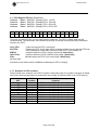
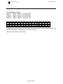
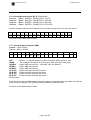
Hytec Electronics Ltd
DIO8005/UTM/1.1
1. PRODUCT DESCRIPTION
The DIO 8005 is a 6U (double height) VME64x digital I/O board constructed to the VME64x
standard. It provides 128 TTL digital I/O bits organised in four groups of 32 bits each with an input
and an output strobe. Each group of 32 bits may be programmed to act as inputs or outputs.
For users familiar with the Hytec 8505 Industry Pack (IP) Card, the 8005 can be considered as 8 x
8505 on a single carrier card, but with the following restrictions…
1. Each block of 32 bits (equivalent to 2 x 8505) can ONLY be set up as All Inputs or All
Outputs.
2. Setting parameters such a de-bounce value, scan rate etc also applies to the whole 32 bit
block.
3. ONLY Internal Clock is available, the 8505 external clock or strobe input options are NOT
available.
When a group is in ‘input mode’, the module features change-of-state detection and contact debounce. A small FIFO memory, one for each input group, allows a historical record of the change-ofstate input data to be stored; up to 64 samples. A further register associated with each input group
controls which bits may generate an interrupt. This function has no effect when in output mode.
When a group is in ‘output mode’, outputs may be programmed as levels or pulses of programmed
duration. A pulse parameter register determines the duration of pulsed outputs up to 100 seconds.
All the above registers occupy I/O space on the card in four groups, starting at offset zero+a (where
a = 000hex, 100hex, 200hex or 300hex) as follows:
Offset
a+0
a+4
a+8
a+C
a+10
a+14
a+18
a+1C
a+20
Name
LKC
CSR
IMR
DBR
PSR
PPR
FIFO_R
LKC_FIFO
IRV
Description
Last Known Change/Data Register
Control and Status Register
Mask Register
De-bounce Register
Pulse Select Register
Pulse Parameter Register
FIFO Register
FIFO Memory
Interrupt Request Vector
The module features hot-swap capability with auto power up and host interaction. An on-board
FPGA allows full mapping of the IP board memory, I/O and ID spaces.
The VME interface supports short I/O access A16:D32:D16:D08 (EO), standard I/O access
A24:D64.D32:D16:D08 (EO).
One of VME bus interrupt lines IRQ1 to IRQ7 can be selected and enabled by writing to an on-board
register. The base address of extended memory can be set by register (offset addressing) or by
geographical addressing lines.
Two groups of four front panel mounted LED’s light to visually indicate when a change of state has
been detected and the scan rate on individual groups (A, B, C and D) of 32 bits. See Table in
Section 7 for more details.
There is a TTL ‘Inhibit’ input on the front panel that allows the user to control when data is written to
the FIFO memory.
Page 3 of 26