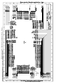
1
Freescale Semiconductor, Inc...
Freescale Semiconductor, Inc. M68360QUADS User’s Manual
M68360QUADS Hardware User’s Manual
Revision 1
August 16, 1993
1
For More Information On This Product,
Go to: www.freescale.com
Thi d
t
t d ith F
M k 404
Freescale Semiconductor, M68360QUADS
Inc.
User’s Manual
GENERAL INFORMATION
CHAPTER 1 - GENERAL INFORMATION
1.1
INTRODUCTION
This manual provides general information, preparation for use and installation instructions, operating
instructions, functional description, and support information for the M68360QUADS QUICC Application
Development System board.
1.2
FEATURES
Freescale Semiconductor, Inc...
The main features of the QUADS board are as follows:
• Master QUICC MC68360 with 32-bit address, 32 or 16 bit data, 25 MHz.
• 1 Mbyte Dynamic RAM, 36 bits wide (data and parity) SIMM.
• 128 Kbyte boot EPROM, 8 bits wide.
• 512 Kbyte Flash Memory, 32 bits wide.
• 256 byte serial EEPROM.
• Application Development Interface (ADI) port connector.
• Serial port with RS-232 connector to terminal or to host computer.
• AppleTalk serial connector.
• BDM Controller capability for external QUICC device.
• Ethernet interface (twisted-pair and AUI) using Motorola MC68160.
• Expansion connectors providing all the signals of the master QUICC.
• Logic analyzer connectors compatible with HP logic analyzers.
• BDM connector for the master QUICC.
• Slave QUICC (core disabled) providing the following functions:
1. DRAM Controller
2. Chip Select and DSACK~ generator.
3. Parallel port (ADI).
4. UART for terminal or host computer connection.
5. AppleTalk controller for MacIntosh computer connection.
6. BDM controller to other QUICC devices.
7. Ethernet controller.
8. Serial EEPROM interface.
9. General Purpose I/O signals.
• HARD RESET, SOFT RESET, and ABORT switches.
• Status LEDs for RUN, HALT, and Ethernet interface.
• 5Vdc and 12Vdc power supply.
2
For More Information On This Product,
Go to: www.freescale.com
Freescale Semiconductor, Inc. M68360QUADS User’s Manual
GENERAL INFORMATION
1.3
SPECIFICATIONS
The M68360QUADS specifications are given in Table 1-1. Paragraph 1.4 details the cooling requirements.
Table 1-1 M68360QUADS Specifications
Freescale Semiconductor, Inc...
CHARACTERISTICS
SPECIFICATIONS
Power requirements (no other boards attached)
+5Vdc @ 3.5 A (typical), 5 A (maximum)
+12Vdc @ 1 A (maximum)
Microprocessor
MC68360 @ 25 MHz
Addressing
Total address range (on and off-board)
Boot EPROM
Flash Memory
Dynamic RAM
EEPROM
4 gigabytes
128 KByte, 8 bits wide
512 KByte, 32 bits wide
1 MByte, 36 bits wide SIMM (32 bit data, 4 bit parity)
option to use higher density SIMM, up to 8 MByte
256 Byte, serial EEPROM
Operating temperature
0 degrees to 30 degrees C ambient air temperature
Storage temperature
-25 degrees to 85 degrees C
Relative humidity
5% to 90% (non-condensing)
Dimensions
Height
Depth
Thickness
9.173 inches (233 mm)
7.087 inches (180 mm)
0.063 inches (1.6 mm)
1.4
COOLING REQUIREMENTS
The M68360QUADS is specified, designed, and tested to operate reliably withan ambient air temperature
range from 0 degrees C to 70 degrees C. Dynamic Burn-in is performed while the board is table mounted
with no other boards attached to it. Test software is executed as the board is subjected to temperature
variations.
If the board is attached to other boards, the thermal conditions may get worse and it is recommended that
the operating temperature should not exceed 30 degrees C.
3
For More Information On This Product,
Go to: www.freescale.com
Freescale Semiconductor, Inc. M68360QUADS User’s Manual
GENERAL INFORMATION
1.5
GENERAL DESCRIPTION
Freescale Semiconductor, Inc...
The M68360QUADS is a development tool for the MC68360 QUICC device. This board is used for
hardware and software development of applications using the QUICC device, such as Ethernet interface
or other communication boards.
The M68360QUADS has logic analyzer connectors and expansion connectors, providing physical
connection to all pins of the master QUICC on the board. The logic analyzer connectors enablethe user to
monitor the bus activity and the I/O pins of the QUICC, by providing direct connection to HP or other logic
analyzers. The expansion connectors enable to attach user applications to the board, and use the board
hardware and software resources to check the user application.
The M68360QUADS has Ethernet and LocalTalk ports, which enable the user to develop and test the
software on the board, before integrating it on the application.
1.6
RELATED DOCUMENTATION
The following publications are applicable to the M68360QUADS and may provide additional helpful
information.
• MC68360 QUICC User’s Manual.
• MC68160 EEST User’s Manual.
1.7
ABBREVIATIONS USED IN THE DOCUMENT
•
•
•
•
•
•
•
•
•
•
•
•
•
1.8
QUICC - QUad Integrated Communications Controller MC68360 device.
EEST - Enhanced Ethernet Serial Transceiver MC68160 device.
QUADS - Application Development System for the QUICC device.
ADI - Application Development Interface.
UART - Universal Asynchronous Receiver/Transmitter.
BDM - Background Debug Mode.
SIMM - Single In-line Memory Module.
AUI - Attachment Unit Interface.
TP - Twisted Pair.
spec - Engineering specification document.
nsec - nano second.
µsec - micro second.
NMI - Non Maskable Interrupt.
REQUIRED EQUIPMENT
The M68360QUADS can operate in two working environments:
• Host controlled
•
Stand-alone
In both operating modes, it is possible to use only 5V power supply. The 12V power supply is required only
if desired on the AUI port or when programming the Flash Memory. (Most AUI Hubs do not require 12 V
supplies to be provided by the network termination equipment).
4
For More Information On This Product,
Go to: www.freescale.com
Freescale Semiconductor, Inc. M68360QUADS User’s Manual
GENERAL INFORMATION
1.8.1
Host controlled setup
Freescale Semiconductor, Inc...
FIGURE 1-1 describes the setup of the host controlled mode of operation. The required equipment in this
mode is as follows:
• +5 V 5 A power supply
• +12 V 1 A power supply (optional)
• Host Computer, one of the following:
o Sun - 4 (SBus interface)
o IBM-PC/XT/AT
• ADI board - compatible with the host computer
• 37 line flat cable with female 37 pin D-type connectors on each end
FIGURE 1-1 Host Controlled Configuration
+12 Vdc
power supply
+5 Vdc
power supply
HOST COMPUTER
P12 P11
M68360QUADS
ADI
P4
37 LINE FLAT CABLE
5
For More Information On This Product,
Go to: www.freescale.com
Freescale Semiconductor, Inc. M68360QUADS User’s Manual
GENERAL INFORMATION
1.8.2
Stand alone setup
FIGURE 1-2 describes the setup of the stand-alone mode of operation. The required equipment in this
mode are as follows:
• +5 V 5 A power supply
• +12 V 1 A power supply (optional)
• VT100 compatible terminal
• RS-232 cable with male 9 pin D-type connector on the QUADS side.
Freescale Semiconductor, Inc...
FIGURE 1-2 Stand-alone Configuration
+12 Vdc
power supply
+5 Vdc
power supply
VT100
compatible terminal
P12 P11
M68360QUADS
P5
RS-232 CABLE
6
For More Information On This Product,
Go to: www.freescale.com
Freescale Semiconductor, Inc. M68360QUADS User’s Manual
HARDWARE PREPARATION AND INSTALLATION
CHAPTER 2 - HARDWARE PREPARATION AND INSTALLATION
2.1
INTRODUCTION
This chapter provides unpacking instructions, hardware preparation, and installation instructions for the
M68360QUADS.
Freescale Semiconductor, Inc...
2.2
UNPACKING INSTRUCTIONS
NOTE
If the shipping carton is damaged upon receipt,
request carrier’s agent be present during
unpacking and inspection of equipment.
Unpack equipment from shipping carton. Refer to packing list and verify that all items are present. Save
packing material for storing and reshipping of equipment.
CAUTION
AVOID TOUCHING AREAS OF INTEGRATED
CIRCUITRY;
STATIC
DISCHARGE
CAN
DAMAGE CIRCUITS.
2.3
HARDWARE PREPARATION
To select the desired configuration and ensure proper operation of the M68360QUADS board, changes of
the Dip-Switch settings may be required before installation. The location of the switches, LEDs, DipSwitches, and connectors is illustrated in FIGURE 2-1. The board has been factory tested and is shipped
with Dip-Switch settings as described in the following paragraphs. Parameters can be changed for the
following conditions:
• ADI port address (Dip-Switch U46).
• Enable/Disable of the following devices on the QUADS (Dip-Switch U52):
- Slave QUICC
- EPROM
- DRAM
•
- Flash Memory
- Clock Generator
- Interrupt Generator
Operation mode of the Master QUICC (Dip-Switch U52):
- Configuring A(31:28) as address lines or write enables.
- Data bus width, 32 or 16 bits.
7
For More Information On This Product,
Go to: www.freescale.com
Flash
Memory
U75
LD2 LD1
U52
ABORT
8
For More Information On This Product,
Go to: www.freescale.com
HARD RESET SW1
SOFT RESET SW2
SW3
P8
Ethernet TP
U46
1
Dip-Switch
1
Dip-Switch
PD5
BDM
to
MASTER
P3
P7
P11
+5V
PD2
P6
PD3
BDM
CONTROL
from
SLAVE
P9
PD1
P5
AppleTalk RS-232 PORT
PD4
F4 F3 F2 F1
2A 2A 5A 5A
P12
+12V
Ethernet AUI
U71
Flash
Memory
U72
EPROM
U48
Flash
Memory
U73
DRAM SIMM
Flash
Memory
U74
PD6
P2
Freescale Semiconductor, Inc...
P1
P4
ADI PORT
U4
SLAVE QUICC
MC68360
U8
MASTER QUICC
MC68360
Freescale Semiconductor, M68360QUADS
Inc.
User’s Manual
HARDWARE PREPARATION AND INSTALLATION
FIGURE 2-1 M68360QUADS Location diagram
Freescale Semiconductor, Inc. M68360QUADS User’s Manual
HARDWARE PREPARATION AND INSTALLATION
2.3.1
ADI Port Address Selection (Dip-Switch U46)
Each M68360QUADS can have eight possible slave addresses set for its ADI port, enabling up to eight
M68360QUADS boards to be connected to the same ADI board in the host computer. The selection of the
slave address is done by setting switches 1, 2, and 3 in the Dip-Switch. Switch 4 is reserved for future use
and it should be in ’OFF’ state. Switch 3 stands for the most-significant bit of the address and switch 1
stands for the least-significant bit. If the switch is in the ’ON’ state, it stands for logical ’1’.
FIGURE 2-2 Dip-Switch configuration for address 0
ON
1
3
4
Freescale Semiconductor, Inc...
2
U46
Table 2-1 describes the switch settings for each slave address:
Table 2-1 ADI Address Selection
ADDRESS
Switch 3
Switch 2
Switch 1
0
OFF
OFF
OFF
1
OFF
OFF
ON
2
OFF
ON
OFF
3
OFF
ON
ON
4
ON
OFF
OFF
5
ON
OFF
ON
6
ON
ON
OFF
7
ON
ON
ON
9
For More Information On This Product,
Go to: www.freescale.com
Freescale Semiconductor, M68360QUADS
Inc.
User’s Manual
HARDWARE PREPARATION AND INSTALLATION
2.3.2
QUADS Operation Mode Configuration (Dip-Switch U52)
Dip-Switch U52 has 8 switches, which are responsible for configuring the operation mode of the master
QUICC on the M68360QUADS, and they also enable devices on the QUADS.
Table 2-2 describes the function of each switch.
Table 2-2 Dip-Switch U52 Description
Default
setting
Function
1
Enable EPROM - This switch connects between the EPROM chip-select input and the
master QUICC CS0~ signal. If the signal CS0~ is used by external logic connected to the
expansion connectors, the switch must be set to OFF to disable the EPROM on the
QUADS. The switch must be set to ON otherwise.
ON
2
Enable slave QUICC - This switch connects between the slave QUICC MBRE~ input pin
and data signal D30. This switch is for factory testing of the QUADS, and it must be set
to ON during normal operation.
ON
3
Enable DRAM - This switch indicates to the master QUICC whether to initialize the
DRAM control registers or not. If the switch is ON, the DRAM on the QUADS is enabled.
If the switch is OFF, the DRAM is disabled, and its memory space is free for the user.
This is useful if the user needs to connect his application to the QUADS expansion
connectors and use the DRAM memory space in the application.
ON
4
Enable Flash Memory - This switch indicates to the master QUICC whether to initialize
the Flash Memory control registers or not. If the switch is ON, the Flash Memory on the
QUADS is enabled. If the switch is OFF, the Flash Memory is disabled, and its memory
space is free for the user. This is useful if the user needs to connect his application to the
QUADS expansion connectors and use the Flash Memory space in the application.
ON
5
A(31:28) Configuration - This switch indicates to the CPU32bug software whether to
configure the master QUICC A(31:28) pins as address lines or as write enable signals. If
the switch is ON, the pins are configured as address lines. If the switch is set to OFF, the
pins are configured as write enable signals.
ON
6
Enable Clock - This switch enables the clock generator on the QUADS. If it is set to ON,
the 25 MHz clock generator is enabled. If it is set to OFF, the clock generator driver is
disabled, and the user must supply clock to the QUADS through pins CLK1 and CLK2 in
the expansion connectors.
ON
7
Enable Interrupt - When this switch is set to ON, it enables the slave QUICC interrupt
generator to drive the master QUICC interrupt input pins. If the switch is set to OFF, the
interrupts to the master QUICC are disabled.
The master QUICC internal interrupt sources are not affected by the position of
this switch.
The user application can drive the master QUICC interrupt pins through the expansion
connectors. When the switch is set to OFF, all external interrupts to the master QUICC
can only be generated by the user application.
ON
Freescale Semiconductor, Inc...
Switch
10
For More Information On This Product,
Go to: www.freescale.com
Freescale Semiconductor, Inc. M68360QUADS User’s Manual
HARDWARE PREPARATION AND INSTALLATION
Table 2-2 Dip-Switch U52 Description
Function
8
Data Bus Configuration - This switch is connected to signal MPRTY3 of the master
QUICC. The level of this signal during hard reset determines the data bus size of the
master QUICC. If the switch is set to OFF, the bus size is 32 bits. If it is set to ON, the
bus size is 16 bits.
In 16 bit mode, interrupt vectors from the slave QUICC do not pass to the master
QUICC, and the auto-vector function must be used.
Note: Power off the QUADS before setting this switch to ON.
Default
setting
OFF
Freescale Semiconductor, Inc...
Switch
11
For More Information On This Product,
Go to: www.freescale.com
Freescale Semiconductor, M68360QUADS
Inc.
User’s Manual
HARDWARE PREPARATION AND INSTALLATION
2.4
INSTALLATION INSTRUCTIONS
When the M68360QUADS has been configured as desired by the user, it can be installed according to the
required working environment as follows:
2.4.1
+5V Power Supply Connection
The M68360QUADS requires +5 Vdc @ 5 A max, power supply for operation. The QUADS has 5A fuses
on the +5V and its ground, and it is protected against reverse connection of the power supply. Connect the
+5V power supply to connector P11 as shown below:
Freescale Semiconductor, Inc...
FIGURE 2-3 P11: +5V Power Connector
VCC
1
Gnd
2
Gnd
3
P11 is a 3 terminal block power connector with power plug. The plug is designed to accept 14 to 22 AWG
wires. It is recommended to use 14 to 18 AWG wires. To insure solid ground, two Gnd terminals are
supplied. It is recommended to connect both Gnd wires to the common of the power supply, while VCC is
connected with a single wire.
NOTE
Since hardware applications can be connected to the
M68360QUADS using the expansion connectors P1 and P2,
the additional power consumption should be taken into
consideration when a power supply is connected to the
QUADS.
2.4.2
+12V Power Supply Connection
The M68360QUADS requires +12 Vdc @ 1 A max, power supply for the Ethernet AUI port, and for
programming the Flash Memory devices. The QUADS can work properly without the +12V power supply,
if the AUI port is not in use or if the AUI port is used with an AUI hub that does not require 12 V to be
provided by the network termination equipment, and if there is no need to reprogram the Flash Memory.
The QUADS has 2A fuses on the +12V and its ground, and it is protected against reverse connection of
the +12V power supply. Connect the +12V power supply to connector P12 as shown below:
FIGURE 2-4 P12: +12V Power Connector
VPP
1
Gnd
2
P12 is a 2 terminal block power connector with power plug. The plug is designed to accept 14 to 22 AWG
wires. It is recommended to use 14 to 18 AWG wires.
12
For More Information On This Product,
Go to: www.freescale.com
Freescale Semiconductor, Inc. M68360QUADS User’s Manual
HARDWARE PREPARATION AND INSTALLATION
2.4.3
ADI Installation
For ADI installation on various host computers, refer to APPENDIX A - on page 54.
2.4.4
Host computer to M68360QUADS Connection
The M68360QUADS ADI interface connector, P4, is a 37 pin, male, D type connector. The connection
between the M68360QUADS and the host computer is by a 37 line flat cable, supplied with the ADI board.
FIGURE 2-5 below shows the pin configuration of the connector.
Freescale Semiconductor, Inc...
FIGURE 2-5 ADI Port Connector
Gnd
Gnd
Gnd
Gnd
Gnd
Gnd
(+ 12 v) N.C.
HOST_VCC
HOST_VCC
HOST_VCC
HOST_ENABLE~
Gnd
Gnd
Gnd
PD0
PD2
PD4
PD6
20
21
22
23
24
25
26
27
28
29
30
31
32
33
34
35
36
37
1
2
3
4
5
6
7
8
9
10
11
12
13
14
15
16
17
18
19
INT_ACK
N.C.
HST_ACK
ADS_ALL
ADS_RESET
ADS_SEL2
ADS_SEL1
ADS_SEL0
HOST_REQ
ADS_REQ
ADS_ACK
ADS_INT
HOST_BRK~
ADS_BRK
N.C.
PD1
PD3
PD5
PD7
NOTE: Pin 26 on the ADI is connected to +12 v power supply, but it is not used in the QUADS.
2.4.5
Terminal to M68360QUADS RS-232 Connection
In the stand-alone operation mode, a VT100 compatible terminal should be connected to the RS-232
connector P5. The RS-232 connector is a 9 pin, female, D-type connector as shown in FIGURE 4-3.
FIGURE 2-6 RS-232 Serial Port Connector
CD
TX
1
2
RX
DTR
3
4
5
GND
6
7
8
9
DSR
RTS
CTS
N.C.
NOTE: The RTS line (pin 7) is not connected in the M68360QUADS.
13
For More Information On This Product,
Go to: www.freescale.com
Freescale Semiconductor, M68360QUADS
Inc.
User’s Manual
OPERATING INSTRUCTIONS
CHAPTER 3 - OPERATING INSTRUCTIONS
3.1
INTRODUCTION
This chapter provides necessary information to use the M68360QUADS in host-controlled and stand-alone
configurations. This includes controls and indicators, memory map details, and software initialization of the
board.
3.2
CONTROLS AND INDICATORS
The M68360QUADS has the following switches and indicators.
Freescale Semiconductor, Inc...
3.2.1
HARD RESET Switch SW1
The HARD RESET switch SW1 resets all QUADS devices, and performs hard reset to the QUICC devices.
The switch signal is debounced, and it is not possible to disable it by software.
This switch must be pressed along with the SOFT RESET switch to activate the hard reset
mechanism. No action is taken if this switch is pressed alone. This feature is intended to protect the
QUICC devices from accidental hard reset.
3.2.2
SOFT RESET Switch SW2
The SOFT RESET switch SW2 resets all QUADS devices, and performs soft reset to the QUICC devices.
The switch signal is debounced, and It is not possible to disable it by software.
3.2.3
ABORT Switch SW3
The ABORT switch is normally used to abort program execution and return control to the CPU32bug. The
slave QUICC provides the ABORT switch interface and it should be programmed as described in section
3.4. The ABORT switch signal is debounced, and if it is enabled by software, it causes a level 7 interrupt
to the master QUICC.
3.2.4
HALT Indicator LD1
The red LED HALT indicator LD1 is lit whenever the master QUICC HALT~ pin is low (asserted).
3.2.5
RUN Indicator LD2
The green LED RUN indicator is connected to the address strobe (AS~) signal. It is lit if the AS~ signal is
low (asserted) and it indicates the activity on the bus.
3.2.6
Ethernet TX Indicator LD3
The green LED Ethernet Transmit indicator LD3 blinks whenever the EEST is transmitting data through
one of the Ethernet ports P7 or P8.
3.2.7
Ethernet RX Indicator LD4
The green LED Ethernet Receive indicator LD4 blinks whenever the EEST is receiving data from one of
the Ethernet ports P7 or P8.
3.2.8
Ethernet CLSN Indicator LD5
The red LED Ethernet Collision indicator LD5 blinks whenever a collision is detected in the AUI P7 port or
the TP P8 port, or a jabber condition is detected in TP mode.
14
For More Information On This Product,
Go to: www.freescale.com
Freescale Semiconductor, Inc. M68360QUADS User’s Manual
OPERATING INSTRUCTIONS
3.2.9
Ethernet TPLIL Indicator LD6
The yellow LED Ethernet Twisted Pair Link Integrity indicator LD6 lights to indicate good link integrity on
the TP P8 port. The LED is off when the link integrity fails, or when the AUI port is selected.
3.2.10
Ethernet TPPLR Indicator LD7
The red LED Ethernet TP Polarity indicator LD7 lights if the wires connected to the receiver input of TP P8
port are reversed. The LED is lit by the EEST, and remains on when the EEST has automatically corrected
for the reversed wires.
3.2.11
Ethernet TPJABB Indicator LD8
Freescale Semiconductor, Inc...
The red LED Ethernet TP Jabber indicator LD8 lights whenever a jabber condition is detected on the TP
P8 port.
3.3
MEMORY MAP
At the beginning of each cycle, the chip-select generators of the master QUICC and the slave QUICC
determine what kind of memory cycle takes place and which device is selected. Cycle types and address
spaces are determined by the function code lines FC3-FC0. The cycle types and the devices that respond
are described in Table 3-1.
Table 3-1 Cycle Types and Responding Devices
FC3-FC0
Address Space
Responding Devices
0000
Reserved
None
0001
User Data
All
0010
User Program
All
0011
Reserved
None
0100
Reserved
None
0101
Supervisor Data
All
0110
Supervisor Program
All
0111
Supervisor CPU
MBAR registers in both QUICC devices and slave QUICC during interrupt
acknowledge cycle.
1XXX
DMA
All
15
For More Information On This Product,
Go to: www.freescale.com
Freescale Semiconductor, M68360QUADS
Inc.
User’s Manual
OPERATING INSTRUCTIONS
3.3.1
Main Memory Map
The memory map of devices that respond in User Data, User Program, Supervisory Data, Supervisory
Program, and DMA spaces is shown in Table 3-2.
Table 3-2 M68360QUADS Main Memory Map
Freescale Semiconductor, Inc...
ADDESS RANGE
Accessed Device
Data Size
NOTES
00000000 - 0001FFFF
Boot EPROM
8
00020000 - 00021FFF
Master QUICC Internal Memory
32
1
00022000 - 00023FFF
Slave QUICC Internal Memory
32
1
00024000 - 00024001
00024002 - 00025FFF
M68360QUADS Status Register
The Status Register appears repeatedly here.
16
2
00026000 - 00026000
00026001 - 00027FFF
Clear NMI Status Registers
This function is repeated here
8
2
00028000 - 00028000
00028001 - 00029FFF
Enable A(31:28)
This function is repeated here
8
2
00080000 - 000FFFFF
Flash Memory
32
00400000 - 004FFFFF
00400000 - 005FFFFF
00400000 - 007FFFFF
00400000 - 00BFFFFF
DRAM SIMM MCM36256
DRAM SIMM MCM36512
DRAM SIMM MCM36100
DRAM SIMM MCM36200
F0000000 - FFFFFFFF
Slave QUICC during interrupt acknowledge cycle
32 + Parity
32
3
4, 5
NOTES:
1. Refer to the MC68360 QUICC User’s Manual for complete description of the QUICC
internal memory.
2. The device appears repeatedly in multiples of its size. For example, the Status Register
appears at memory locations 00024000, 00024002, 00024004 etc...
3. The DRAM SIMM installed in the M68360QUADS is MCM36256 256Kx36 bit. The user
may replace the DRAM module with higher density SIMM, and increase the DRAM space
up to 8 MByte.
4. The master QUICC can not read the interrupt vector generated by the slave QUICC if it is
configured to work in 16 bit mode. The auto-vector function must be used in this mode.
5. External interrupting devices connected to the QUADS must use the auto-vector function,
because the interrupt acknowledge address space is occupied by the slave QUICC.
3.3.2
CPU Address Space
The master QUICC can generate four types of CPU space cycles: Breakpoint Acknowledge, LPSTOP
broadcast, MBAR access, and Interrupt Acknowledge (IACK). The Breakpoint Acknowledge cycle is not
supported in the M68360QUADS. The LPSTOP broadcast cycle can be generated because it does not
need a response from an external device. The slave and master QUICCs respond when their MBAR are
accessed. The IACK cycle is supported in the M68360QUADS by the slave QUICC, which functions as the
interrupt handler on the board and it responds to the IACK cycle.
16
For More Information On This Product,
Go to: www.freescale.com
Freescale Semiconductor, Inc. M68360QUADS User’s Manual
OPERATING INSTRUCTIONS
3.4
Programming the master QUICC
The master QUICC internal registers must be programmed after hardware reset as described in the
following paragraphs. The addresses and programming values are in hexadecimal base.
Please refer to the MC68360 QUICC User’s Manual for more information.
3.4.1
Module Base Address Register
The master QUICC’s module base address register (MBAR) controls the location of its internal memory
and registers and their access space. The master QUICC MBAR resides at a fixed location in ’0003FF00’
in the CPU space. The MBAR must be initialized to ’00020001’ to obtain the memory map as described in
Table 3-2.
Freescale Semiconductor, Inc...
3.4.2
Module Configuration Register
The MCR controls the SIM60 configuration in the master QUICC. The BSTM bit in the MCR must be set
to ’0’. This setting will enable using asynchronous timing on the bus signals.
3.4.3
Auto Vector Register
The auto vector register (AVR) contains 8 bits that correspond to external interrupt levels that require an
auto vector response. The AVR must be initialized to 84 to generate auto vectors for interrupt levels 7 and
2. These interrupts are generated through the slave QUICC without supplying interrupt vectors during an
IACK cycle.
3.4.4
Reset Status Register
The reset status register (RSR) indicates the source of the last reset that occurred, when the relevant bit
is set. This register must be cleared after every reset, so that when the next reset occurs, its source can
be easily determined. The register is cleared by writing ’FF’.
3.4.5
CLKO Control Register
The CLKO control register (CLKOCR) controls the operation of the CLKO(0:1) pins. This register must be
initialized to ’AB’, so that the CLKO1 pin is disabled and the CLKO2 pin is enabled with 1/3 strength output
buffer.
3.4.6
PLL Control Register
The PLL control register (PLLCR) controls the operation of the PLL. There is no need to program the
PLLCR after hard reset, because the configuration of the MODCK(0:1) pins on the QUADS determines its
value. It is recommended to set the PLLWR bit to prevent accidental writing.
3.4.7
Port E Pin Assignment Register
Port E pins can be programmed by the port E pin assignment register (PEPAR). The A(31:28) pins of the
master QUICC can be programmed as address lines or as write enable W(0:3)~ lines. Bit 7 in the PEPAR
must be cleared to select address lines function, and it must be set to select the write enable function. Until
this bit is written, the A(31:28) pins are three-stated.
3.4.8
System Protection Control
The system protection register (SYPCR) controls the system monitors, the software watchdog, and the bus
monitor timing. This register must be initialized to ’37’ to disable the software watchdog, and to enable the
bus monitor function.
17
For More Information On This Product,
Go to: www.freescale.com
Freescale Semiconductor, M68360QUADS
Inc.
User’s Manual
OPERATING INSTRUCTIONS
3.4.9
Global Memory Register
The global memory register (GMR) contains selections for the memory controller of the master QUICC.
The SYNC bit must be set and the EMWS bit must be cleared, to obtain synchronous operation of the
memory controller when the DMA in the slave QUICC is active.
3.4.10
Base Register 0 and Option Register 0
Base register 0 (BR0) and Option register 0 (OR0) control the operation of CS0~ pin of the master QUICC.
The Boot EPROM in the M68360QUADS is connected to this pin. BR0 must be initialized to ’00000003’,
and OR0 must be initialized to ’5FFE0004’ to obtain the memory map as described in Table 3-2.
3.5
Programming the slave QUICC
Freescale Semiconductor, Inc...
The slave QUICC (core disabled) provides the following functions on the M68360QUADS:
1. DRAM Controller
2. Chip Select and DSACK~ generator.
3. Parallel port (ADI).
4. UART for terminal or host computer connection.
5. AppleTalk controller for MacIntosh computer connection.
6. BDM controller to other QUICC devices.
7. Ethernet controller.
8. Serial EEPROM interface.
9. General Purpose I/O signals.
The slave QUICC internal registers must be programmed after hardware reset as described in the following
paragraphs. The addresses and programming values are in hexadecimal base.
Please refer to the MC68360 QUICC User’s Manual for more information.
3.5.1
Module Base Address Register
The slave QUICC’s module base address register (MBAR) controls the location of its internal memory and
registers and their access space. The slave QUICC MBAR resides at a fixed location in ’0003FF04’ in the
CPU space. Before accessing the MBAR, the software must write to the module base address register
enable (MBARE), which resides at fixed location in ’0003FF08’ in the CPU space.
The MBARE~ pin of the slave QUICC is connected to data line D30, therefore the MBARE register must
be initialized to ’BFFFFFFF’ before initializing the MBAR.
The MBAR must be initialized to ’00022001’ to obtain the memory map as described in Table 3-2.
Note: If the master QUICC data bus is configured to operate in 16 bit mode, the MBARE must be written
with ’BFFF’ before each word access to the MBAR.
3.5.2
Module Configuration Register
The module configuration register (MCR) controls the SIM60 configuration in the slave QUICC. The BSTM
bit in the MCR must be set to ’0’. This setting will enable using asynchronous timing on the bus signals.
3.5.3
CLKO Control Register
The CLKO control register (CLKOCR) controls the operation of the CLKO(0:1) pins. This register must be
initialized to ’AF’, so that the CLKO(0:1) pins of the slave QUICC are disabled.
3.5.4
PLL Control Register
The PLL control register (PLLCR) controls the operation of the PLL. There is no need to program the
PLLCR after hard reset, because the configuration of the MODCK(0:1) pins on the QUADS determines its
value. It is recommended to set the PLLWR bit to prevent accidental writing.
18
For More Information On This Product,
Go to: www.freescale.com
Freescale Semiconductor, Inc. M68360QUADS User’s Manual
OPERATING INSTRUCTIONS
3.5.5
Port E Pin Assignment Register
Port E pins can be programmed by the port E pin assignment register (PEPAR). The PEPAR must be
initialized to ’3760’ to configure Port E of the slave QUICC as follows:
• The output of the slave QUICC interrupt request is on IOUT(0:2)~ pins.
• RAS1~ and RAS2~ double drive function is used to drive the DRAM.
• The A(31:28) pins of the slave QUICC are configured as address lines.
• The OE~/AMUX pin is configured as AMUX to drive the external multiplexers of the DRAM.
• The CAS(0:3)~ output function is used for the DRAM.
• CS7~ output function is enabled.
Freescale Semiconductor, Inc...
3.5.6
System Protection Control
The system protection register (SYPCR) controls the system monitors, the software watchdog, and the bus
monitor timing. This register must be initialized to ’37’ to disable the software watchdog and to enable the
bus monitor function in the slave QUICC.
3.5.7
Global Memory Register
The global memory register (GMR) contains selections for the memory controller of the slave QUICC. The
GMR must be initialized according to the size and the access time of the DRAM SIMM installed on the
M68360QUADS as follows:
• For 70 nsec DRAM type MCM36256 or MCM36100, the GMR must be initialized to ’17840380’.
• For 70 nsec DRAM type MCM36512 or MCM36200, the GMR must be initialized to ’0A840380’.
• For 80 nsec DRAM type MCM36256 or MCM36100, the GMR must be initialized to ’17A40380’.
• For 80 nsec DRAM type MCM36512 or MCM36200, the GMR must be initialized to ’0AA40380’.
• For 100 nsec DRAM type MCM36256 or MCM36100, the GMR must be initialized to ’17A44380’.
• For 100 nsec DRAM type MCM36512 or MCM36200, the GMR must be initialized to ’0AA44380’.
The GMR defines the following parameters:
• The DRAM refresh period is 15.36 µsec.
• The DRAM refresh cycle length depends on the DRAM access time, and it is either 3 clocks or 4
clocks long.
• The DRAM module port size is 32 bits.
• The parity is disabled.
• The CS~/RAS~ lines of the slave QUICC will not assert when accessing the CPU space.
• Internal address multiplexing for the DRAM is disabled.
3.5.8
Base Register 0 and Option Register 0
Base register 0 (BR0) and Option register 0 (OR0) control the operation of CS0~ pin of the slave QUICC.
This pin has no connection on the M68360QUADS, but CS0~ and CS7~ are used to distinguish between
accesses to the board internal resources and external devices that may be attached to the board. BR0
must be initialized to ’00000003’, and OR0 must be initialized to ’FFFE0006’, for proper operation of the
board.
19
For More Information On This Product,
Go to: www.freescale.com
Freescale Semiconductor, M68360QUADS
Inc.
User’s Manual
OPERATING INSTRUCTIONS
3.5.9
Base Register 1 and Option Register 1
Freescale Semiconductor, Inc...
Base register 1 (BR1) and Option register 1 (OR1) control the operation of RAS1~ pin of the slave QUICC.
This pin is connected to the DRAM module. These registers must be initialized according to the type of the
DRAM SIMM installed on the M68360QUADS as follows:
• OR1 must be initialized to ’2FF00009’ for 70 nsec or 80 nsec DRAM, types MCM36256 or
MCM36512.
• OR1 must be initialized to ’3FF00009’ for 100 nsec DRAM, types MCM36256 or MCM36512.
• OR1 must be initialized to ’2FC00009’ for 70 nsec or 80 nsec DRAM, type MCM36100 or
MCM36200.
• OR1 must be initialized to ’3FC00009’ for 100 nsec DRAM, type MCM36100 or MCM36200.
BR1 must be initialized to ’00400005’, disregarding the type and the access time of the DRAM.
Note: The CPU32bug software does not access BR1 and OR1 after reset if the Enable DRAM switch in
U52 is in ’OFF’ position.
The software must perform 8 accesses to the RAS1~ address space after initialization for proper operation
of the DRAM.
3.5.10
Base Register 2 and Option Register 2
Base register 2 (BR2) and Option register 2 (OR2) control the operation of RAS2~ pin of the slave QUICC.
This pin is connected to the DRAM module. These registers must be initialized if the type of the DRAM
SIMM installed on the M68360QUADS is MCM36512 or MCM36200, because these two types contain two
DRAM banks, and RAS1~ can not be connected to both banks.
If the DRAM SIMM type is MCM36512, BR2 must be initialized to ’00500005’. OR2 must be initialized to
’2FF00009’ for 70 nsec or 80 nsec DRAM, and to ’3FF00009’ for 100 nsec DRAM.
If the DRAM SIMM type is MCM36200, BR2 must be initialized to ’00800005’. OR2 must be initialized to
’2FC00009’ for 70 nsec or 80 nsec DRAM, and to ’3FC00009’ for 100 nsec DRAM.
Note: The CPU32bug software does not access BR2 and OR2 after reset if the Enable DRAM switch in
U52 is in ’OFF’ position.
The software must perform 8 accesses to the RAS2~ address space after initialization for proper operation
of the DRAM.
3.5.11
Base Register 3 and Option Register 3
Base register 3 (BR3) and Option register 3 (OR3) control the operation of CS3~ pin of the slave QUICC.
The Flash Memory on the M68360QUADS is connected to this pin. BR3 must be initialized to ’00080009’,
and OR3 must be initialized to ’3FF80000’ to obtain the memory map as described in Table 3-2.
Note: The CPU32bug software does not access BR3 and OR3 after reset if the Enable Flash Memory
switch in U52 is in ’OFF’ position.
3.5.12
Base Register 4 and Option Register 4
Base register 4 (BR4) and Option register 4 (OR4) control the operation of CS4~ pin of the slave QUICC.
The M68360QUADS Status Register is connected to this pin. BR4 must be initialized to ’00024003’, and
OR4 must be initialized to ’0FFFE002’ to obtain the memory map as described in Table 3-2.
3.5.13
Base Register 5 and Option Register 5
Base register 5 (BR5) and Option register 5 (OR5) control the operation of CS5~ pin of the slave QUICC.
The M68360QUADS has Abort Register that is set by the Abort switch and Host NMI Register that is set
by the host computer connected to the ADI port. Setting either register generates a level 7 interrupt to the
master QUICC. The CS5~ signal is used on the M68360QUADS by the interrupt handling routine to clear
these registers. BR5 must be initialized to ’00026001’, and OR5 must be initialized to ’0FFFE004’ to obtain
the memory map as described in Table 3-2.
20
For More Information On This Product,
Go to: www.freescale.com
Freescale Semiconductor, Inc. M68360QUADS User’s Manual
OPERATING INSTRUCTIONS
3.5.14
Base Register 6 and Option Register 6
Base register 6 (BR6) and Option register 6 (OR6) control the operation of CS6~ pin of the slave QUICC.
The A(31:28) pins of the master QUICC can be configured as address lines or as write enable lines. After
hard reset, these lines are in three-state condition until the PEPAR of the master QUICC is written. If the
A(31:28) Configuration switch in U52 is ’ON’, the CPU32bug software initializes the PEPAR in the master
QUICC, and asserts the CS6~ signal to enable using the A(31:28) as address lines on the board. BR6 must
be initialized to ’00028001’, and OR6 must be initialized to ’0FFFE004’ to obtain the memory map as
described in Table 3-2.
Note: If the A(31:28) pins are used as write enable lines, CS6~ must never be asserted. It is recommended
to initialize BR6 to ’00028000’ to avoid accidental accesses to the address space of CS6~.
Freescale Semiconductor, Inc...
3.5.15
Base Register 7 and Option Register 7
Base register 7 (BR7) and Option register 7 (OR7) control the operation of CS7~ pin of the slave QUICC.
CS0~ and CS7~ are used to distinguish between accesses to the board internal resources and external
devices that may be attached to the board. For proper operation of the board, BR7 must be initialized to
’00000001’, and OR7 must be initialized to ’F0000006’.
3.5.16
Port A Open Drain Register
Port A of the slave QUICC is 16 pins port, and each pin may be configured as general purpose I/O pin or
as dedicated peripheral interface pin. The port A open drain register (PAODR) configures the drivers of
port A pins as open-drain or as active drivers. The PAODR must be initialized to ’0000’ to select the active
drivers configuration.
3.5.17
Port A Data Register
Port A data register (PADAT) can be read to check the data at the pin. If a port pin is configured as general
purpose output pin, the value in the PADAT for that pin is driven onto the pin. It is recommended to initialize
PADAT to ’FFFF’ before configuring the other port registers.
3.5.18
Port A Data Direction Register
The port A data direction register (PADIR) has different functions according to the configuration of the port
pins. If a pin is general purpose I/O pin, the value in the PADIR for that pin defines the direction of the pin.
If a pin is dedicated peripheral interface pin, the value in the PADIR for that pin may select one of two
dedicated functions of the pin. The PADIR must be initialized to ’3C00’.
3.5.19
Port A Pin Assignment Register
The port A pin assignment register (PAPAR) configures the function of the port pins. If the value in the
PAPAR for a pin is ’0’ the pin is general purpose I/O, otherwise the pin is dedicated peripheral interface
pin. The PAPAR must be initialized to ’033F’.
3.5.20
Port B Open Drain Register
Port B of the slave QUICC is 18 pins port, and each pin may be configured as general purpose I/O pin or
as dedicated peripheral interface pin. The port B open drain register (PBODR) configures the drivers of
port B pins as open-drain or as active drivers. The PBODR must be initialized to ’0000’ to select the active
drivers configuration.
3.5.21
Port B Data Register
Port B data register (PBDAT) can be read to check the data at the pin. If a port pin is configured as general
purpose output pin, the value in the PBDAT for that pin is driven onto the pin. It is recommended to initialize
PBDAT to ’3FFFF’ before configuring the other port registers.
21
For More Information On This Product,
Go to: www.freescale.com
Freescale Semiconductor, M68360QUADS
Inc.
User’s Manual
OPERATING INSTRUCTIONS
3.5.22
Port B Data Direction Register
The port B data direction register (PBDIR) has different functions according to the configuration of the port
pins. If a pin is general purpose I/O pin, the value in the PBDIR for that pin defines the direction of the pin.
If a pin is dedicated peripheral interface pin, the value in the PBDIR for that pin may select one of two
dedicated functions of the pin. The PBDIR must be initialized to ’0007F’. Pins 10 to 17 are connected to
the ADI port data bus, therefore their direction must be changed by software according to the data flow.
3.5.23
Port B Pin Assignment Register
The port B pin assignment register (PBPAR) configures the function of the port pins. If the value in the
PBPAR for a pin is ’0’ the pin is general purpose I/O, otherwise the pin is dedicated peripheral interface
pin. The PBPAR must be initialized to ’0000E’.
3.5.24
Port C Data Register
Freescale Semiconductor, Inc...
Port C of the slave QUICC is 12 pin port, and each pin may be configured as general purpose I/O pin or
as dedicated peripheral interface pin, with interrupt capability. Port C data register (PCDAT) can be read
to check the data at the pin. If a port pin is configured as general purpose output pin, the value in the
PCDAT for that pin is driven onto the pin. It is recommended to initialize PCDAT to ’0740’ before configuring
the other port registers.
3.5.25
Port C Data Direction Register
The port C data direction register (PCDIR) has different functions according to the configuration of the port
pins. If a pin is general purpose I/O pin, the value in the PCDIR for that pin defines the direction of the pin.
If a pin is dedicated peripheral interface pin, the value in the PCDIR for that pin may select one of three
dedicated functions of the pin. The PCDIR must be initialized to ’0F8C’.
3.5.26
Port C Pin Assignment Register
The port C pin assignment register (PCPAR) configures the function of the port pins, along with PCDIR and
PCSO. The PCPAR must be initialized to ’0003’.
3.5.27
Port C Special Options Register
The port C special options register (PCSO) configures the CDx and CTSx pins. Port C can detect changes
on the CTS and CD lines, and assert the corresponding interrupt while the SCC simultaneously uses those
lines. The PCSO must be initialized to ’0030’.
22
For More Information On This Product,
Go to: www.freescale.com
Freescale Semiconductor, Inc. M68360QUADS User’s Manual
FUNCTIONAL DESCRIPTION
CHAPTER 4 - FUNCTIONAL DESCRIPTION
4.1
INTRODUCTION
This chapter details the hardware design of the M68360QUADS, and describes each module.
Freescale Semiconductor, Inc...
4.2
Master QUICC
The CPU of the master QUICC device, U8 in sheet 4, is the main processor on the QUADS. The working
frequency of the QUICC is 25 Mhz, but the user can change the frequency by replacing the oscillator U27
in sheet 5. The frequency of the oscillator is twice the working frequency of the board.
The master QUICC can be configured to operate either in 32 bit mode or 16 bit mode, according to the
level of MPRTY3 signal during hard reset. The user can drive this signal low (16 bit mode) either by
selecting this mode in Dip-Switch U52 (Sheet 14), or by driving it through the expansion connector P2
(Sheet 21).
In 16 bit mode, the data transceivers (Sheet 6) and the data bus controller (Sheet 8) control the data flow
between the 16 bit data bus of the master QUICC and the 32 bit devices on the QUADS, by directing the
data to the proper lines. There is one restriction on the software so that it can support both operating
modes, provided that it uses the auto-vector function of the master QUICC. If the slave QUICC interrupts
the master QUICC, the master can read the interrupt vector only in 32 bit mode. When programming the
MBAR register in the slave QUICC, it must access it in two 16 bit transfers, and it must write to the MBARE
register before each access. This restriction is due to the design of the QUICC, which requires writing to
the MBARE register before accessing the MBAR register, therefore when the QUICC operates in 16 bit
mode, it can not access the MBAR in 32 bit transfers.
All the pins of the master QUICC device are available unbuffered to the user through the expansion
connectors P1 and P2 (Sheets 20 and 21), and the logic analyzer connectors PD1 to PD6 (Sheets 18 and
19). The user can monitor the QUICC activity and connect the QUADS to his own hardware application
during its development stage. The logic analyzer connectors PD1 to PD5 can be connected directly to HP
logic analyzers.
The master QUICC pins are buffered from all the devices on the QUADS, to minimize their load and to
enable easy connection to the user hardware application.
The BDM pins of the master QUICC are also available for the user through connector P3 (Sheet 16). This
connector can be used to download code and to monitor functions.
4.3
Boot EPROM
The boot EPROM is the 27C010 device U48 in sheet 2 (200 nsec access time, 128K x 8 bit) and is used
to store the debug and the boot programs. The EPROM is accessed as 8 bit device, using the Global CS
port of the master QUICC.
It is possible for the user to disable accesses to the EPROM on the QUADS, and to use the Global CS port
to access his own EPROM on his application board after reset. This is done by setting the Enable EPROM
switch in U52 to ’OFF’, thus disconnecting the M_CS0~ signal from E_CS~ signal.
23
For More Information On This Product,
Go to: www.freescale.com
Freescale Semiconductor, M68360QUADS
Inc.
User’s Manual
FUNCTIONAL DESCRIPTION
FIGURE 4-1 HARDWARE BLOCK DIAGRAM
P3
BDM
Connector
PD1 - PD6
Logic Analyzer Connectors
QUICC
(master)
P1 and P2
Expansion Connectors
Freescale Semiconductor, Inc...
128 KByte
Boot EPROM
(8 bits wide)
Transceivers
Status
Register
Local Bus Arbiter
Bus Controller
512 KByte
Flash Memory
(32 bits wide)
1 MByte DRAM
with parity
(36 bits wide SIMM)
QUICC
(slave)
256 Byte
Serial
EEPROM
MC68160
EEST
BDM Controller Port
ADI Port
RS-232 Port
AppleTalk Port
Ethernet Port
RJ-45 Connector
Ethernet Port
AUI Connector
P9
P4
P5
P6
P8
P7
4.4
Flash Memory
Four Flash Memory devices, the 28F010 (128 KByte, 120 nsec access time) are used to form 512 Kbyte
program storage memory. The devices, U72 to U75 in sheet 2, are organized as long-word (32 bits wide).
The Flash Memory devices are soldered to the board, and program code updates will be done on board
without the need for external EPROM programmer. The programming software is stored in the boot
EPROM, which loads the new code through one of the QUADS ports, erases the Flash Memory, and
programs the new code.
24
For More Information On This Product,
Go to: www.freescale.com
Freescale Semiconductor, Inc. M68360QUADS User’s Manual
FUNCTIONAL DESCRIPTION
The slave QUICC device provides the F_CS~ signal to the Flash Memory. The user must connect external
12v power supply to connector P12 to program the devices.
The user may indicate to the CPU32bug software not to initialize BR3 and OR3 registers in the slave
QUICC by setting the Enable Flash Memory switch in U52 to OFF. This setting is used to disable accesses
to the Flash Memory after hard reset, and its address space may be used by the user.
4.5
EEPROM
Freescale Semiconductor, Inc...
The EEPROM used in the QUADS is Motorola MCM2814 256 byte serial EEPROM (U33 in sheet 2). The
slave QUICC SPI port (port B pins 0 to 3) is used to control accesses to the EEPROM.
The MCM2814 has internal hardware protection against inadvertent writes to the EEPROM that might
happen at power up or power down time.
4.6
DRAM
The QUADS is supplied with 1 Mbyte of Dynamic RAM, which is implemented by the MCM36256S80
DRAM module. The module, U71 in sheet 1, is a 72 lead SIMM, 80 nsec access time, organized as 256K
x 36 bit for data and parity signals.
It is possible to replace the supplied DRAM SIMM with a higher density module, in order to increase the
DRAM memory space up to 8 Mbyte. The higher density modules, such as the MCM36200, may require
using RAS1 and RAS2 signals of the slave QUICC, because they are organized as two memory banks.
These signals are supplied to the DRAM socket in the QUADS, so that the user does not need to do any
wiring.
The SIMM has four presence detect signals, SIMM1 to SIMM4, which can be read by the software through
the Status Register (U61 and U39 in sheet 14). The CPU32bug software determines the DRAM memory
space and access time according to these signals, as described in Table 4-1.
Table 4-1 DRAM SIMM Types
SIMM(4:1)
SIMM Type
SIMM Organization
Access Time
(nsec)
Control
Signals
0000
MCM36100S10
1M x 36
100
RAS1
0001
MCM36512S10
512K x 36
100
RAS1, RAS2
0010
MCM36256S10
256K x 36
100
RAS1
0011
MCM36200S10
2M x 36
100
RAS1, RAS2
0100
MCM36100S80
1M x 36
80
RAS1
0101
MCM36512S80
512K x 36
80
RAS1, RAS2
0110
MCM36256S80
256K x 36
80
RAS1
0111
MCM36200S80
2M x 36
80
RAS1, RAS2
1000
MCM36100S70
1M x 36
70
RAS1
1001
MCM36512S70
512K x 36
70
RAS1, RAS2
1010
MCM36256S70
256K x 36
70
RAS1
1011
MCM36200S70
2M x 36
70
RAS1, RAS2
1100
Not Valid
1101
Not Valid
1110
Not Valid
1111
Not Valid
25
For More Information On This Product,
Go to: www.freescale.com
Freescale Semiconductor, M68360QUADS
Inc.
User’s Manual
FUNCTIONAL DESCRIPTION
The DRAM is controlled by the slave QUICC device, using its DRAM Controller function for normal
accesses, page mode accesses, and refresh accesses. The DRAM can be accessed by the master
QUICC, the slave QUICC (the IDMA and the SDMA are not disabled), and external bus master connected
to the expansion connectors of the QUADS.
The user may indicate to the CPU32bug software not to initialize BR1, OR1, BR2, and OR2 registers in the
slave QUICC by setting the Enable DRAM switch in U52 to OFF. This setting is used to disable accesses
to the DRAM after hard reset, and its address space may be used by the user.
Note: The CPU32bug software requires 8 KByte of RAM space located at address 00400000. If the
DRAM is disabled, the user must connect external RAM to the QUADS for the software to run
properly.
4.7
Slave QUICC
Freescale Semiconductor, Inc...
During normal operation, the CPU of the slave QUICC (U4 in sheet 3) is disabled, and the device is used
to implement the following functions on the QUADS:
1. DRAM Controller
2. Chip Select and DSACK~ generator.
3. Parallel port (ADI).
4. UART for terminal or host computer connection.
5. AppleTalk controller for MacIntosh computer connection.
6. BDM controller to other QUICC devices.
7. Ethernet controller.
8. Serial EEPROM interface.
9. General Purpose I/O signals.
The address of the MBAR register is configured to be at $0033FF04. The master QUICC must write the
MBARE register at address $0033FF08 before each access to the slave MBAR register.
The slave QUICC is essential to make the master QUICC pins available for the user implementations. The
QUICC peripherals (such as the IDMA and SDMA) can request the bus and become bus master, while the
CPU is disabled.
4.7.1
DRAM Controller
The slave QUICC device provides the necessary control signals for the DRAM module. The software on
the QUADS reads the presence detect pins of the SIMM, and sets the DRAM Controller parameters
according to the DRAM module, and the access time of the DRAM.
The hardware connection of the slave QUICC to the DRAM module is straight forward. External address
multiplexers (U67, U62, and U53 in sheet 1) are used to drive the DRAM address lines, to enable external
bus masters to access the DRAM. The CPU32bug software programs the PEPAR so that the OE~/AMUX
pin of the slave QUICC is configured as AMUX to drive the address multiplexers.
The RAS1~ and RAS2~ pins of the slave QUICC drive the DRAM SIMM. The double-drive signals
RAS1DD~ and RAS2DD~ also drive the DRAM to decrease signal load.
4.7.2
Chip Select and DSACK~ generator
The slave QUICC device provides the Chip Select signals to the QUADS devices as follows:
1. CS0~ pin of the slave QUICC is not connected to any device on the QUADS, but its
function is used along with CS7~ by the bus control logic to distinguish between accesses
to the board devices and external devices that may be attached to the board.
2. CS1~ and CS2~ are connected to the DRAM SIMM, and they act as RAS1~ and RAS2~.
3. CS3~ is connected to the Flash Memory (U72, U73, U74, and U75 in sheet 2).
26
For More Information On This Product,
Go to: www.freescale.com
Freescale Semiconductor, Inc. M68360QUADS User’s Manual
FUNCTIONAL DESCRIPTION
4. CS4~ is connected to the M68360QUADS Status Register (U61 and U39 in sheet 14).
5. CS5~ is connected to the Abort and Host NMI registers, U68 in sheet 7 and U31 in sheet
12. This signal is used to clear these registers after interrupt level 7.
6. CS6~ is connected to the Enable Address register, U22 in sheet 5. This signal is used to
enable using A(31:28) lines of the master QUICC as address lines on the QUADS.
7. CS7~ is connected to the Bus Controller, U51 in sheet 8. If this signal is negated, it
indicates that the current access is to a device on the QUADS. The DSACK~ generator is
disabled for this signal.
Freescale Semiconductor, Inc...
4.7.3
ADI Port (Sheet 12)
The ADI parallel port supplies parallel link from the QUADS to various host computers. This port is
connected via a 37 line cable to a special board called ADI (Application Development Interface) installed
in the host computer. It is possible to connect the QUADS board to an IBM-PC/XT/AT or to SUN-4 SPARC
station, provided that they have an ADI board with the appropriate software drivers installed on them.
Each QUADS can have 8 possible slave addresses set for its ADI port, enabling up to 8 QUADS boards
to be connected to the same ADI board. The QUADS address is selected by U46 in sheet 9.
The ADI port connector P4 is a 37 pin, male, D type connector. The connection between the QUADS and
the host computer is by a 37 line flat cable, supplied with the ADI board. FIGURE 4-2 below shows the pin
configuration of the connector.
FIGURE 4-2 ADI Port Connector
Gnd
Gnd
Gnd
Gnd
Gnd
Gnd
(+ 12 v) N.C.
HOST_VCC
HOST_VCC
HOST_VCC
HOST_ENABLE~
Gnd
Gnd
Gnd
PD0
PD2
PD4
PD6
20
21
22
23
24
25
26
27
28
29
30
31
32
33
34
35
36
37
1
2
3
4
5
6
7
8
9
10
11
12
13
14
15
16
17
18
19
INT_ACK
N.C.
HST_ACK
ADS_ALL
ADS_RESET
ADS_SEL2
ADS_SEL1
ADS_SEL0
HOST_REQ
ADS_REQ
ADS_ACK
ADS_INT
HOST_BRK~
ADS_BRK
N.C.
PD1
PD3
PD5
PD7
NOTE: Pin 26 on the ADI is connected to +12 v power supply, but it is not used in the QUADS.
27
For More Information On This Product,
Go to: www.freescale.com
Freescale Semiconductor, M68360QUADS
Inc.
User’s Manual
FUNCTIONAL DESCRIPTION
4.7.3.1
ADI Port Signal Description
Freescale Semiconductor, Inc...
The ADI port on the M68360QUADS was slightly modified to generate either hard reset or soft reset. This
feature was added to comply with the QUICC reset mechanism. The host software written for the
M68360QUADS should be able to work properly with existing QUADS boards, such as the M68302ADS.
In the list below, the directions ’I’, ’O’, and ’I/O’ are relative to the QUADS board. (I.E. ’I’ means input to the
QUADS)
• ADS_SEL(0:2) - ’I’
These three input lines determine the slave address of the QUADS being accessed by the host
computer. Up to 8 boards can be addressed by one ADI board.
• ADS_ALL - ’I’
This input line is used to reset or abort program execution on all QUADS development boards that
are connected to the same ADI board.
• HOST_ENABLE~ - ’I’
This line is always driven low by the ADI board. The QUADS software uses this line to determine
if a host is connected to the ADI port.
• ADS_BRK - ’I’
When a host is connected, this line is used in conjunction with the addressing lines or with the
ADS_ALL line to generate a non-maskable interrupt (interrupt level 7) to the QUICC.
• ADS_RESET - ’I’
When a host is connected, this line is used in conjunction with the addressing lines or with the
ADS_ALL line to reset the QUADS board. The type of the reset, hard or soft, is determined by
INT_ACK signal.
• HOST_REQ - ’I’
This signal initiates a host to QUADS write cycle.
• ADS_ACK - ’O’
This signal is the QUADS response to the HOST_REQ signal, indicating that the QUADS board
has detected the assertion of HOST_REQ.
• ADS_REQ - ’O’
This signal initiates an QUADS to host write cycle.
• HST_ACK - ’I’
This signal serves as the host’s response to the ADS_REQ signal.
• HOST_BRK~ - ’O’
This open-collector signal generates an interrupt to the host. This signal is common to all QUADS
boards that are connected to the same ADI.
• ADS_INT - ’O’
This line is polled by the host computer during its interrupt acknowledge cycle to determine which
QUADS board has generated the interrupt.
• INT_ACK - ’I’
This line is asserted by the host at the end of its interrupt acknowledge cycle. This signal is used
by the QUADS hardware to negate the HOST_BRK~ signal. The software in the QUADS must
negate the ADS_INT signal upon detecting the assertion of INT_ACK to support the daisy-chain
interrupt structure.
This line is also used by the host to generate either hard reset or soft reset. In this case, this line
is used in conjunction with ADS_RESET, and with either the addressing lines or with the
ADS_ALL line.
28
For More Information On This Product,
Go to: www.freescale.com
Freescale Semiconductor, Inc. M68360QUADS User’s Manual
FUNCTIONAL DESCRIPTION
•
•
4.7.4
HOST_VCC - ’I’ (three lines)
These lines are power lines from the host computer. In the QUADS, these lines are used by the
software to determine if the host computer is powered on. The QUADS does not use these lines
for power supply.
PD(0:7) - ’I/O’
These eight I/O lines are the parallel data bus. This bus is used to transmit and receive data from
the host computer.
RS-232 Serial Port (Sheet 11)
The serial port is provided by the slave QUICC SCC3 serial channel. The M68360QUADS can be
connected to a VT100 compatible terminal or to a host computer through the serial port.
The RS-232 serial port connector P5 is a 9 pin, female, D-type connector as shown in FIGURE 4-3.
Freescale Semiconductor, Inc...
FIGURE 4-3 RS-232 Serial Port Connector
CD
TX
1
2
RX
DTR
3
4
5
GND
4.7.4.1
6
7
8
9
DSR
RTS
CTS
N.C.
RS-232 Port Signal Description
In the list below, the directions ’I’, ’O’, and ’I/O’ are relative to the QUADS board. (I.E. ’I’ means input to the
QUADS)
• CD ( O ) - Data Carrier Detect. This line is always asserted by the QUADS.
• TX ( O ) - Transmit Data.
• RX ( I ) - Receive Data.
• DTR ( I ) - Data Terminal Ready. This signal is used by the software in the QUADS to detect if a
terminal is connected to the QUADS board.
• DSR ( O ) - Data Set Ready. This line is always asserted by the QUADS.
• RTS ( I ) - Request To Send. This line is not connected in the QUADS.
• CTS ( O ) - Clear To Send. This line is always asserted by the QUADS.
4.7.5
AppleTalk Port (Sheet 11)
The AppleTalk port is provided by the slave QUICC SCC2 serial channel. The AppleTalk is the 230.4 kbps
local area network that connects multiple MacIntosh computers and printers.
The AppleTalk port connector P6 is 8 pin, MINI DIN JACK connector as shown in FIGURE 4-4.
FIGURE 4-4 AppleTalk Connector
8 N.C. 6
7
5
GND 3
4
RX2
1
RX+
HSKI
TX+
TX-
+5V
29
For More Information On This Product,
Go to: www.freescale.com
Freescale Semiconductor, M68360QUADS
Inc.
User’s Manual
FUNCTIONAL DESCRIPTION
4.7.5.1
AppleTalk Port Signal Description
In the list below, the directions ’I’, ’O’, and ’I/O’ are relative to the QUADS board. (I.E. ’I’ means input to the
QUADS)
• +5V ( O ) - 5V output from the QUADS through 100 ohm resistor.
• HSKI ( I ) - Hand Shake Input.
• TX- ( O ) - Transmit Data (negative).
• RX- ( I ) - Receive Data (negative).
• TX+ ( O ) - Transmit Data (positive).
• RX+ ( I ) - Receive Data (positive).
4.7.6
BDM Controller (Sheet 16)
Freescale Semiconductor, Inc...
The slave QUICC enables the M68360QUADS to become BDM controller to control other QUICC devices
on the user application. The BDM feature enables the user to download code and provides hardware and
software debugging capability of the user application.
The 8 pin BDM connector P9 utilizes five pins of the slave QUICC port B. These pins are configured as
general purpose I/O pins.
4.7.7
Ethernet Controller (Sheet 10)
The slave QUICC provides Ethernet port for the M68360QUADS by connecting SCC1 to Motorola
MC68160 EEST device (U35 in sheet 10). The MC68160 provides two Ethernet interfaces, twisted-pair on
P8 and AUI on P7. The LEDs LD3-LD8 are controlled by the EEST, and they provide indications about the
status of the Ethernet ports activity.
The signals between the slave QUICC and the MC68160 appear on connector P10 for debugging
purposes. P10 is a set of wire holes.
The socket U24 is installed for internal factory testing only. For proper operation of the EEST, this socket
must be empty.
4.7.7.1
Ethernet AUI Port Signal Description
The AUI port connector P7 is a 15 pin, female, D-type connector as shown in FIGURE 4-3.
FIGURE 4-5 Ethernet AUI Port Connector
GND
ACX+
ATX+
GND
1
2
3
4
5
ARX+
GND 6
N.C. 7
GND 8
9 ACX10 ATX11
12
13
14
15
GND
ARX+12V
GND
N.C.
30
For More Information On This Product,
Go to: www.freescale.com
Freescale Semiconductor, Inc. M68360QUADS User’s Manual
FUNCTIONAL DESCRIPTION
The list below describes the port signals. The directions ’I’, ’O’, and ’I/O’ are relative to the QUADS board.
(I.E. ’I’ means input to the QUADS)
• ACX+ ( I ) - Collision Input (positive).
• ATX+ ( O ) - Transmit Data (positive).
• ARX+ ( I ) - Receive Data (positive).
• ACX- ( I ) - Collision Input (negative).
• ATX- ( O ) - Transmit Data (negative).
• ARX- ( I ) - Receive Data (negative).
• +12V ( O ) - +12V power supply from the QUADS.
4.7.7.2
Ethernet Twisted-Pair Port Signal Description
Freescale Semiconductor, Inc...
The twisted-pair port connector P8 is a 8 pin, RJ-45 connector as shown in FIGURE 4-3.
FIGURE 4-6 Ethernet Twisted-Pair Port Connector
TPTX+
TPTX-
1
TPRX+
N.C.
N.C.
3
4
5
TPRXN.C.
N.C.
6
7
8
2
The list below describes the port signals. The directions ’I’, ’O’, and ’I/O’ are relative to the QUADS board.
(I.E. ’I’ means input to the QUADS)
• TPTX+ ( O ) - Transmit Data (positive).
• TPTX- ( O ) - Transmit Data (negative).
• TPRX+ ( I ) - Receive Data (positive).
• TPRX- ( I ) - Receive Data (negative).
4.7.8
Serial EEPROM Interface (Sheet 2)
The MCM2814 serial EEPROM (U33 in sheet 2) is 256 bytes EEPROM with SPI interface. It is controlled
by the SPI port of the slave QUICC (pins 1,2 and 3 of port B), and by a general purpose output pin (pin 0
of port B). The SPI port operates in master mode.
4.7.9
Slave QUICC General Purpose I/O Pins
The slave QUICC has three ports, A, B, and C, whose pins can be individually configured by software to
be general purpose I/O pin or dedicated peripheral function. The QUICC also has another port, E, whose
pins are not general purpose I/O, but they can be configured to operate in one of two possible modes.
The following subsections describe the slave QUICC ports. Refer to section 3.5 on page 18 for the required
programming information.
31
For More Information On This Product,
Go to: www.freescale.com
Freescale Semiconductor, M68360QUADS
Inc.
User’s Manual
FUNCTIONAL DESCRIPTION
4.7.9.1
Slave QUICC Port A
Port A is 16 pins port. Table 4-2 describes the configuration of port A.
Table 4-2 Port A Pins Description
Freescale Semiconductor, Inc...
Pin
Pin Name
Description
0
Ethernet RX
This pin is connected to the receive data output of the EEST. It is configured as the
receive data of SCC1 in the slave QUICC.
1
Ethernet TX
This pin is connected to the transmit data input of the EEST. It is configured as the
transmit data of SCC1 in the slave QUICC.
2
AppleTalk RX
This pin is connected to the receive data output of the AppleTalk transceiver U29. It is
configured as the receive data of SCC2 in the slave QUICC.
3
AppleTalk TX
This pin is connected to the transmit data input of the AppleTalk transceiver U29. It is
configured as the transmit data of SCC2 in the slave QUICC.
4
RS-232 RX
This pin is connected to the receive data output of the RS-232 transceiver U23. It is
configured as the receive data of SCC3 in the slave QUICC.
5
RS-232 TX
This pin is connected to the transmit data input of the RS-232 transceiver U23. It is
configured as the transmit data of SCC3 in the slave QUICC.
6
Enable DRAM
This pin is connected to switch 3 in dip-switch U52. It is configured as input pin in the
slave QUICC, and its level indicates to the CPU32bug software if it should enable
accesses to the DRAM on the QUADS. If the level is ’0’, the DRAM is enabled.
7
Enable Flash
This pin is connected to switch 4 in dip-switch U52. It is configured as input pin in the
slave QUICC, and its level indicates to the CPU32bug software if it should enable
accesses to the Flash Memory on the QUADS. If it is ’0’, the Flash is enabled.
8
Ethernet TCLK
This pin is connected to the transmit clock output of the EEST. It is configured as the
transmit clock of SCC1 in the slave QUICC.
9
Ethernet RCLK
This pin is connected to the receive clock output of the EEST. It is configured as the
receive clock of SCC1 in the slave QUICC.
10
ADS G~
This pin is connected to the ADI port logic. It is configured as output pin in the slave
QUICC, and it is used by the ADI logic to control the ADI data transceiver.
11
ADS INT~
This pin is connected to the ADI port signal ADS_INT through the buffer U16. It is
configured as output pin in the slave QUICC, and it is also used by the ADI logic to
interrupt the host computer.
12
ADS ACK~
This pin is connected to the ADI port signal ADS_ACK through the buffer U16. It is
configured as output pin in the slave QUICC.
13
ADS REQ~
This pin is connected to the ADI port signal ADS_REQ through the buffer U16. It is
configured as output pin in the slave QUICC.
14
VPP ON
This pin is configured as input pin, and it is used to sense the +12V power supply. If it
is ’1’, +12V is applied to the QUADS.
15
Spare
This pin is connected to switch 4 of dip-switch U46, and it is configured as input pin in
the slave QUICC. It has no function on the ADS, and it is reserved for future
applications.
32
For More Information On This Product,
Go to: www.freescale.com
Freescale Semiconductor, Inc. M68360QUADS User’s Manual
FUNCTIONAL DESCRIPTION
4.7.9.2
Slave QUICC Port B
Port B is 18 pins port. Table 4-2 describes the configuration of port B.
Freescale Semiconductor, Inc...
Table 4-3 Port B Pins Description
Pin
Pin Name
Description
0
EEPROM
Select
This pin is connected to the select input of the EEPROM, and it is configured as
output pin in the slave QUICC.
1
EEPROM CLK
This pin is connected to the clock input of the EEPROM, and it is configured as the
SPI clock of the slave QUICC.
2
EEPROM
Serial In
This pin is connected to the serial data input of the EEPROM, and it is configured as
the SPI MOSI of the slave QUICC.
3
EEPROM
Serial Out
This pin is connected to the serial data output of the EEPROM, and it is configured as
the SPI MISO of the slave QUICC.
4
BDM CLK
This pin is connected to the BDM Controller connector P9. It is configured as output
pin in the slave QUICC.
5
BDM Reset
This pin is connected to the BDM Controller connector P9. It is configured as output
pin in the slave QUICC.
6
BDM Data Out
This pin is connected to the BDM Controller connector P9. It is configured as output
pin in the slave QUICC.
7
BDM Data In
This pin is connected to the BDM Controller connector P9. It is configured as input pin
in the slave QUICC.
8
This pin is not connected on the QUADS board.
9
BDM Freeze
This pin is connected to the BDM Controller connector P9. It is configured as input pin
in the slave QUICC.
10
ADI Data 0
This pin is connected to the ADI port signal PD0 through the data bus transceiver U2,
and it is configured as I/O pin.
11
ADI Data 1
This pin is connected to the ADI port signal PD0 through the data bus transceiver U2,
and it is configured as I/O pin.
12
ADI Data 2
This pin is connected to the ADI port signal PD0 through the data bus transceiver U2,
and it is configured as I/O pin.
13
ADI Data 3
This pin is connected to the ADI port signal PD0 through the data bus transceiver U2,
and it is configured as I/O pin.
14
ADI Data 4
This pin is connected to the ADI port signal PD0 through the data bus transceiver U2,
and it is configured as I/O pin.
15
ADI Data 5
This pin is connected to the ADI port signal PD0 through the data bus transceiver U2,
and it is configured as I/O pin.
16
ADI Data 6
This pin is connected to the ADI port signal PD0 through the data bus transceiver U2,
and it is configured as I/O pin.
17
ADI Data 7
This pin is connected to the ADI port signal PD0 through the data bus transceiver U2,
and it is configured as I/O pin.
33
For More Information On This Product,
Go to: www.freescale.com
Freescale Semiconductor, M68360QUADS
Inc.
User’s Manual
FUNCTIONAL DESCRIPTION
4.7.9.3
Slave QUICC Port C
Port C is 12 pins port. Table 4-2 describes the configuration of port C.
Table 4-4 Port C Pins Description
Freescale Semiconductor, Inc...
Pin
Pin Name
Description
0
TENA
This pin is connected to the TENA input of the EEST. It is configured as the RTS
signal of SCC1 in the slave QUICC.
1
AppleTalk
Enable
This pin is connected to the enable input of the AppleTalk transceiver U29. It is
configured as the RTS signal of SCC2 of the slave QUICC. If this pin is ’0’, the
transceiver output to the AppleTalk port P6 is enabled.
2
EEST CS2
This pin is connected to the CS2 input of the EEST, and it is configured as output pin
in the slave QUICC. If this pin is ’1’, the EEST operates in standby mode, and if it is
’0’, the EEST is in normal operation mode.
3
TPEN
This pin is connected to the TPEN I/O pin of the EEST, and it is configured as I/O pin
in the slave QUICC. The TPEN (Twisted-Pair Port Enable) pin in the EEST
determines which port is selected to operate, AUI or TP.
4
CLSN
This pin is connected to the CLSN output of the EEST. It is configured as the CTS
signal of SCC1 in the slave QUICC.
5
RENA
This pin is connected to the RENA output of the EEST. It is configured as the CD
signal of SCC1 in the slave QUICC.
6
HSKI
This pin is connected to the HSKI signal of the AppleTalk port through the transceiver
U29. It is configured as the CTS signal of SCC2 of the slave QUICC.
7
APORT
This pin is connected to the APORT input of the EEST, and it is configured as output
pin in the slave QUICC. If this pin is ’1’, the EEST automatically select the TP or AUI
port based on the TP receive input. If it is ’0’, the TPEN pin selects the operating port.
8
TPAPCE
This pin is connected to the TPAPCE input of the EEST, and it is configured as output
pin in the slave QUICC. If this pin is ’1’, automatic polarity correction is enabled on
the TP port.
9
TPSQEL
This pin is connected to the TPSQEL input of the EEST, and it is configured as output
pin in the slave QUICC. If this pin is ’0’, it enables testing the EEST internal TP
collision detect circuitry.
10
TPFULDL
This pin is connected to the TPFULDL input of the EEST, and it is configured as
output pin in the slave QUICC. If this pin is ’0’, it allows simultaneous transmit and
receive operation on the TP port without an indicated collision.
11
LOOP
This pin is connected to the LOOP input of the EEST, and it is configured as output
pin in the slave QUICC. This pin enables diagnostic loopback in the EEST.
34
For More Information On This Product,
Go to: www.freescale.com
Freescale Semiconductor, Inc. M68360QUADS User’s Manual
FUNCTIONAL DESCRIPTION
4.7.9.4
Slave QUICC Port E
Port E pins can be configured to operate in one of two dedicated peripheral functions. The PEPAR register
configures the operation mode, as described in section 3.5.5 on page 19.
Freescale Semiconductor, Inc...
4.8
LOCAL BUS ARBITER (Sheet 9)
The local bus master can be one of the following:
• The master QUICC.
• An External Bus Master connected to the QUADS through the expansion connectors.
• The slave QUICC peripherals (One of the DMA channels, DRAM refresh, etc...).
The master QUICC is the local bus master during normal operation. The Local Bus Arbiter, U42 in sheet
9, is PAL16R4 device that uses the master QUICC arbitration logic to transfer the bus mastership to other
masters.
The M68360QUADS has provision for the user to connect External Bus Master device to the local bus
through the Expansion Connectors P1 and P2. The relevant control signals (EXTBR~, EXTBG~, and
BGACK~) appear on connector P1. The arbitration priority from highest to lowest is slave QUICC, External
Bus Master, and master QUICC.
The Bus Arbiter output signal A_DIR controls the direction of the address bus transceivers (U7, U6, U5,
U28, U14, and U21 in sheet 5) between the master QUICC and the other devices on the QUADS.
U42 also generates the output signal A28_31, which is used by the data bus controller to determine the
direction of the data bus transceivers.
4.9
DATA BUS CONTROLLER (Sheet 8)
The data and parity bus transceivers (U20,U15, U32, U12, U25, U13, U11, U18, and U19 in sheet 6) are
controlled by a GAL22V10 device, U51 in sheet 8. U51 also generates the Byte Enable signals according
to the accessed address and the data size.
The signals CS7~ of the slave QUICC and A28_31 of U42 are used to indicate if the current access is to
one of the devices on the QUADS. The CS7~ signal is programmed for the address range 00000000 to
0FFFFFFF hexadecimal, with its DSACK generator disabled. The signal CS0~ of the slave QUICC is
programmed to cover the address range of the Boot EPROM, so that CS7~ is not asserted if the EPROM
is accessed. CS7~ is asserted if none of the slave QUICC chip-select signals is asserted, so If CS7~ is
asserted (low), this indicates that the accessed device is not on the QUADS board.
The A28_31 signal is high if any of the upper four address bits A28 to A31 is high, or if external EPROM is
accessed instead of the M68360QUADS Boot EPROM. If A28_31 is high, it indicates that the accessed
device is not on the QUADS board.
The GAL22V10 device also control the data bus swapping if the master QUICC is configured to operate in
16 bits mode.
4.10
Status Register (Sheet 14)
The M68360QUADS Status Register consists of two 74LS373 devices (U61 and U39 in sheet 14) that form
16 bit read-only device. The register in controlled by CS4~ of the slave QUICC.
35
For More Information On This Product,
Go to: www.freescale.com
Freescale Semiconductor, M68360QUADS
Inc.
User’s Manual
FUNCTIONAL DESCRIPTION
The Status Register bits are described in Table 4-5 below:
Table 4-5 Status Register Description
Freescale Semiconductor, Inc...
Bit No.
Description
0
Data Bus Configuration - This bit indicates the operation mode of the master QUICC data bus. If it is
’1’, the data bus is in 32 bit mode. If it is ’0’, the data bus is in 16 bit mode.
1
Interrupt Enable - This bit indicates if interrupts from the QUADS devices to the master QUICC are
enabled. If this bit is ’0’, the master QUICC may be interrupted by the QUADS resources, such as the
ABORT switch and the slave QUICC peripherals.
2
Clock Source - This bit indicates the source of the clock on the QUADS. If it is ’1’, the clock is supplied
to the QUADS through the expansion connector P1. If the bit is ’0’, the clock is supplied by the
QUADS clock generator.
3
A(31:28) Pins Configuration - These bits indicates to the CPU32bug software the required configuration of the master QUICC A(31:28) pins. If it is ’1’, the pins are configured as write enable signals. If it
is ’0’, the pins are configured as address lines.
4
SIMM1 - This bit is connected to the DRAM SIMM presence detect signals. Refer to Table 4-1 for
complete description of the available DRAM types, and their SIMM(4:1) codes.
5
SIMM2 - This bit is connected to the DRAM SIMM presence detect signals. Refer to Table 4-1 for
complete description of the available DRAM types, and their SIMM(4:1) codes.
6
SIMM3 - This bit is connected to the DRAM SIMM presence detect signals. Refer to Table 4-1 for
complete description of the available DRAM types, and their SIMM(4:1) codes.
7
SIMM4 - This bit is connected to the DRAM SIMM presence detect signals. Refer to Table 4-1 for
complete description of the available DRAM types, and their SIMM(4:1) codes.
8
Host VCC - This bit is connected to the ADI port. If it is ’0’, it indicates that the host computer is
powered on.
9
Host Enable - This bit is connected to the ADI port. If it is ’1’, it indicates that the ADI port is connected
to a host computer.
10
Host Ack - This bit is connected to the ADI port. If it is ’0’, it indicates that the host has responded to
the ADS REQ signal.
11
Host Req - This bit is connected to the ADI port. If it is ’0’, it indicates that the host is requesting to
write to the QUADS.
12
ADS Select - This bit is connected to the ADI port. If it is ’1’, it indicates that the host computer has
selected the QUADS for the current data transfer.
13
Interrupt Ack - This bit is connected to the ADI port. If it is ’0’, it indicates that the host has responded
to the interrupt signal from the QUADS.
14
Host NMI - This bit is connected to the ADI port. If it is ’0’, it indicates that the host has generated a
level 7 interrupt to the QUADS.
15
DTR~ - Data Terminal Ready indication. This bit indicates if a terminal is connected to the RS-232
Serial Port.
36
For More Information On This Product,
Go to: www.freescale.com
Freescale Semiconductor, Inc. M68360QUADS User’s Manual
FUNCTIONAL DESCRIPTION
4.11
Interrupt Logic
The slave QUICC is configured by the CPU32bug software to assert its interrupt requests on its IOUT(2:0)~
pins. The 74F538 decoder (U70 in sheet 13) accepts the IOUT signals and decodes them to select one of
the master QUICC IRQ(7:1)~ signals. The IRQ signals of the master QUICC are driven by open-collector
devices, so that the user application connected to the expansion connectors P1 and P2 may assert them
along with the interrupt logic on the QUADS board.
It is possible to disable U70 from driving the IRQ signals, so that the master QUICC can only be interrupted
by its internal peripherals or by the user application. This is done by setting the Enable Interrupt switch in
U52 to ’OFF’.
Freescale Semiconductor, Inc...
FIGURE 4-7 Interrupt Logic Configuration
ABORT
Switch
Host
NMI
ADI Port
Activity
IRQ7~
IRQ2~
slave
QUICC
IOUT(2:0)~
74F538
Decoder
74LS05
Open-Collector
Device
IRQ(7:1)~
master
QUICC
Enable
Interrupt
U52
Dip-Switch
Expansion Connectors P1 and P2
The slave QUICC accepts interrupts from the ABORT switch, the Host NMI register, and the ADI port logic.
These interrupt sources are encoded by the slave QUICC, along with interrupts from its internal
peripherals, and highest interrupt level is driven on the IOUT(2:0)~ pins. The slave QUICC may supply
interrupt vector during interrupt acknowledge cycle for its internal interrupts, but it can not do that for the
external interrupts. Therefore, the master QUICC must be programmed to provide auto-vector for interrupts
in levels 2 and 7.
If the QUADS is configured to operate in 16 bit mode, the master QUICC can not read the interrupt vector
generated by the slave QUICC during interrupt acknowledge cycles. In this case the auto-vector function
must be used.
If an external interrupting device is connected to the QUADS, the auto-vector function must be used to
handle its interrupts. This is because the interrupt acknowledge address space is occupied by the slave
QUICC, and the external interrupter may not drive data during interrupt acknowledge cycles.
4.12
Disable CPU Logic for the Slave QUICC (Sheet 15)
The slave QUICC must be configured to work with its CPU disabled, its global CS disabled, and its MBAR
to reside at address 3FF04. For this, the encoding of its configuration pins CONFIG(2:0) must enable the
CPU for more than 32 clocks during hard reset, and then they must be encoded to ’110’ before the hard
reset signal is negated (high level).
The CONFIG2 and CONFIG1 pins are connected to pull-up resistors on the QUADS. The CONFIG0 pin is
driven by a PAL22V10-25 device, SP1 in sheet 15, during hard reset. SP1 drives CONFIG0 to high level
for 64 clock cycles after the hard reset signal is asserted. This makes the encoding of CONFIG(2:0) pins
equals ’111’ which enables the CPU. After 64 clocks, the CONFIG0 pin is driven low as long as the hard
reset signal is asserted.
37
For More Information On This Product,
Go to: www.freescale.com
Freescale Semiconductor, M68360QUADS
Inc.
User’s Manual
FUNCTIONAL DESCRIPTION
Freescale Semiconductor, Inc...
When the hard reset signal is negated, the CPU of the slave QUICC is disabled, and SP1 stops driving the
CONFIG0 pin.
38
For More Information On This Product,
Go to: www.freescale.com
Freescale Semiconductor, Inc. M68360QUADS User’s Manual
SUPPORT INFORMATION
CHAPTER 5 - SUPPORT INFORMATION
5.1
INTRODUCTION
This chapter provides the interconnection signals, parts list, and schematic diagrams of the
M68360QUADS board.
Freescale Semiconductor, Inc...
5.2
INTERCONNECT SIGNALS
The M68360QUADS board interconnects with external devices through the following connectors:
• PD1 - PD5 are five 20 pin, male connectors, compatible with HP logic analyzer connectors, that
provides the bus signals of the master QUICC for bus monitoring.
• PD6 is 96 pin, male, logic analyzer connector providing the remaining signals of the master
QUICC.
• P1 and P2 are two 96 pin, female, expansion connectors providing all the signals of the master
QUICC for connection to the user hardware application.
• P3 is 8 pin male connector connected to the BDM pins of the master QUICC.
• P4 is 37 pin, male D type connector, for the ADI port.
• P5 is 9 pin, female D type connector, for the RS-232 port.
• P6 is 8 pin, MINI DIN JACK connector, for the AppleTalk port.
• P7 is 15 pin, female D type connector, for AUI connection to the Ethernet port.
• P8 is 8 pin, RJ-45 connector, for twisted-pair connection to the Ethernet port.
• P9 is 8 pin male connector. It is the BDM controller connector that enables the QUADS to control
the activity of external QUICC mounted on the user application board.
• P10 is 16 wire holes on the board. The signals between the slave QUICC and the EEST appear
on P10 for internal factory debugging purposes.
• P11 is 3 pin connector for 5v power supply input: GND (x2) and +5V
• P12 is 2 pin connector for 12v power supply input: GND and +12V
5.2.1
Connector PD1 Interconnect Signals
Connector PD1 is a double-row, 20 pin, male connector. The lower 16 address lines of the master QUICC
appear on this connector for easy monitoring of the bus by a logic analyzer. Table 5-1 describes the
connector signals.
Table 5-1 Connector PD1 Interconnect Signals
Pin No.
1
2
3
4
5
6
7
8
9
Signal Name
Description
CLK1
A15
A14
A13
A12
A11
A10
Not connected
Not connected
The operating clock of the M68360QUADS, 25 MHz.
Address line 15 of the master QUICC (unbuffered).
Address line 14 of the master QUICC (unbuffered).
Address line 13 of the master QUICC (unbuffered).
Address line 12 of the master QUICC (unbuffered).
Address line 11 of the master QUICC (unbuffered).
Address line 10 of the master QUICC (unbuffered).
39
For More Information On This Product,
Go to: www.freescale.com
Freescale Semiconductor, M68360QUADS
Inc.
User’s Manual
SUPPORT INFORMATION
Table 5-1 Connector PD1 Interconnect Signals
Freescale Semiconductor, Inc...
Pin No.
10
11
12
13
14
15
16
17
18
19
20
5.2.2
Signal Name
Description
A9
A8
A7
A6
A5
A4
A3
A2
A1
A0
GND
Address line 9 of the master QUICC (unbuffered).
Address line 8 of the master QUICC (unbuffered).
Address line 7 of the master QUICC (unbuffered).
Address line 6 of the master QUICC (unbuffered).
Address line 5 of the master QUICC (unbuffered).
Address line 4 of the master QUICC (unbuffered).
Address line 3 of the master QUICC (unbuffered).
Address line 2 of the master QUICC (unbuffered).
Address line 1 of the master QUICC (unbuffered).
Address line 0 of the master QUICC (unbuffered).
Ground signal of the M68360QUADS.
Connector PD2 Interconnect Signals
Connector PD2 is a double-row, 20 pin, male connector. The higher 16 address lines of the master QUICC
appear on this connector for easy monitoring of the bus by a logic analyzer. Table 5-1 describes the
connector signals.
Table 5-2 Connector PD2 Interconnect Signals
Pin No.
1
2
3
4
5
6
7
8
9
10
11
12
13
14
15
16
17
18
19
20
Signal Name
Description
DSACK0~
A31
A30
A29
A28
A27
A26
A25
A24
A23
A22
A21
A20
A19
A18
A17
A16
GND
Not connected
Not connected
DSACK0~ line of the master QUICC.
Address line 31 of the master QUICC (unbuffered).
Address line 30 of the master QUICC (unbuffered).
Address line 29 of the master QUICC (unbuffered).
Address line 28 of the master QUICC (unbuffered).
Address line 27 of the master QUICC (unbuffered).
Address line 26 of the master QUICC (unbuffered).
Address line 25 of the master QUICC (unbuffered).
Address line 24 of the master QUICC (unbuffered).
Address line 23 of the master QUICC (unbuffered).
Address line 22 of the master QUICC (unbuffered).
Address line 21 of the master QUICC (unbuffered).
Address line 20 of the master QUICC (unbuffered).
Address line 19 of the master QUICC (unbuffered).
Address line 18 of the master QUICC (unbuffered).
Address line 17 of the master QUICC (unbuffered).
Address line 16 of the master QUICC (unbuffered).
Ground signal of the M68360QUADS.
40
For More Information On This Product,
Go to: www.freescale.com
Freescale Semiconductor, Inc. M68360QUADS User’s Manual
SUPPORT INFORMATION
5.2.3
Connector PD3 Interconnect Signals
Connector PD3 is a double-row, 20 pin, male connector. The lower 16 data lines of the master QUICC
appear on this connector for easy monitoring of the bus by a logic analyzer. Table 5-1 describes the
connector signals.
Table 5-3 Connector PD3 Interconnect Signals
Freescale Semiconductor, Inc...
Pin No.
1
2
3
4
5
6
7
8
9
10
11
12
13
14
15
16
17
18
19
20
5.2.4
Signal Name
Description
DSACK1~
D15
D14
D13
D12
D11
D10
D9
D8
D7
D6
D5
D4
D3
D2
D1
D0
GND
Not connected
Not connected
DSACK1~ line of the master QUICC.
Data line 15 of the master QUICC (unbuffered).
Data line 14 of the master QUICC (unbuffered).
Data line 13 of the master QUICC (unbuffered).
Data line 12 of the master QUICC (unbuffered).
Data line 11 of the master QUICC (unbuffered).
Data line 10 of the master QUICC (unbuffered).
Data line 9 of the master QUICC (unbuffered).
Data line 8 of the master QUICC (unbuffered).
Data line 7 of the master QUICC (unbuffered).
Data line 6 of the master QUICC (unbuffered).
Data line 5 of the master QUICC (unbuffered).
Data line 4 of the master QUICC (unbuffered).
Data line 3 of the master QUICC (unbuffered).
Data line 2 of the master QUICC (unbuffered).
Data line 1 of the master QUICC (unbuffered).
Data line 0 of the master QUICC (unbuffered).
Ground signal of the M68360QUADS.
Connector PD4 Interconnect Signals
Connector PD4 is a double-row, 20 pin, male connector. The higher 16 data lines of the master QUICC
appear on this connector for easy monitoring of the bus by a logic analyzer. Table 5-1 describes the
connector signals.
Table 5-4 Connector PD4 Interconnect Signals
Pin No.
1
2
3
4
5
6
7
8
Signal Name
Description
DS~
D31
D30
D29
D28
D27
Not connected
Not connected
Data Strobe line of the master QUICC.
Data line 31 of the master QUICC (unbuffered).
Data line 30 of the master QUICC (unbuffered).
Data line 29 of the master QUICC (unbuffered).
Data line 28 of the master QUICC (unbuffered).
Data line 27 of the master QUICC (unbuffered).
41
For More Information On This Product,
Go to: www.freescale.com
Freescale Semiconductor, M68360QUADS
Inc.
User’s Manual
SUPPORT INFORMATION
Table 5-4 Connector PD4 Interconnect Signals
Freescale Semiconductor, Inc...
Pin No.
Signal Name
Description
9
10
11
12
13
14
15
16
17
18
19
D26
D25
D24
D23
D22
D21
D20
D19
D18
D17
D16
Data line 26 of the master QUICC (unbuffered).
Data line 25 of the master QUICC (unbuffered).
Data line 24 of the master QUICC (unbuffered).
Data line 23 of the master QUICC (unbuffered).
Data line 22 of the master QUICC (unbuffered).
Data line 21 of the master QUICC (unbuffered).
Data line 20 of the master QUICC (unbuffered).
Data line 19 of the master QUICC (unbuffered).
Data line 18 of the master QUICC (unbuffered).
Data line 17 of the master QUICC (unbuffered).
Data line 16 of the master QUICC (unbuffered).
20
GND
Ground signal of the M68360QUADS.
5.2.5
Connector PD5 Interconnect Signals
Connector PD5 is a double-row, 20 pin, male connector. The master QUICC bus control signals appear on
this connector for easy monitoring of the bus by a logic analyzer. Table 5-1 describes the connector signals.
Table 5-5 Connector PD5 Interconnect Signals
Pin No.
1
2
3
4
5
6
7
8
9
10
11
12
13
14
15
16
17
18
19
20
Signal Name
Description
AS~
BERR~
PERR~
IFETCH~
IPIPE0~
IPIPE1~
FREEZE
FC3
DSACK1~
DSACK0~
FC2
FC1
FC0
SIZ1
SIZ0
R/W~
BGACK~
GND
Not connected
Not connected
Address Strobe
Bus Error
Parity Error
Instruction Fetch
Instruction Pipe 0
Instruction Pipe 1
Freeze
Function Code 3
Data and Size Acknowledge 1
Data and Size Acknowledge 0
Function Code 2
Function Code 1
Function Code 0
Transfer Size 1
Transfer Size 0
Read / Write
Bus Grant Acknowledge
Ground signal of the M68360QUADS.
42
For More Information On This Product,
Go to: www.freescale.com
Freescale Semiconductor, Inc. M68360QUADS User’s Manual
SUPPORT INFORMATION
5.2.6
Connector PD6 Interconnect Signals
Connector PD6 is a triple-row, 96 pin, male DIN connector. The remaining signals of the master QUICC
appear on this connector. Table 5-1 describes the connector signals.
Table 5-6 Connector PD6 Interconnect Signals
Freescale Semiconductor, Inc...
Pin No.
A1 - A16
A17
A18 - A21
A22, A23
A24 - A30
A31
A32
B1 - B18
B19
B20 - B31
B32
C1 - C4
C5
C6 - C13
C14
C15
C16
C17
C18
C19
C20
C21
C22
C23
C24
C25
C26
C27
C28
C29
C30
C31
C32
Signal Name
Description
PA0 - PA15
VCC
PRTY0 - PRTY3
GND
IRQ1~ - IRQ7~
AVEC~
GND
PB0 - PB17
GND
PC0 - PC11
GND
CAS0~ - CAS3~
VCC
CS0~ - CS7~
HALT~
AMUX
TCK
TMS
TDI
TDO
TRST~
BKPT~
RESETH~
RESETS~
CONFIG0
CONFIG1
TRIS~
MODCK0
MODCK1
GND
CLKO2
GND
CLK2
Port A pins 0 to 15 of the master QUICC
+5V
Parity lines 0 to 3
Ground signal of the M68360QUADS
Interrupt request signals 1 to 7 of the master QUICC
Auto vector pin of the master QUICC
Ground signal of the M68360QUADS
Port B pins 0 to 17 of the master QUICC
Ground signal of the M68360QUADS
Port C pins 0 to 11 of the master QUICC
Ground signal of the M68360QUADS
CAS signals 0 to 3 of the master QUICC
+5V
Chip select signals 0 to 7 of the master QUICC
HALT~ pin of the master QUICC
AMUX/OE~ pin of the master QUICC
TCK pin of the master QUICC
TMS pin of the master QUICC
TDI pin of the master QUICC
TDO pin of the master QUICC
TRST~ pin of the master QUICC
Breakpoint pin of the master QUICC
Hard reset pin of the master QUICC
Soft reset pin of the master QUICC
RMC~/CONFIG0 pin of the master QUICC
CONFIG1 pin of the master QUICC
TRIS~ pin of the master QUICC
Clock mode select 0 pin of the master QUICC
Clock mode select 1 pin of the master QUICC
Ground signal of the M68360QUADS
System clock out 2 pin of the master QUICC, 50 MHz.
Ground signal of the M68360QUADS
The operating clock of the M68360QUADS, 25 MHz.
43
For More Information On This Product,
Go to: www.freescale.com
Freescale Semiconductor, M68360QUADS
Inc.
User’s Manual
SUPPORT INFORMATION
5.2.7
Connector P1 Interconnect Signals
Connector P1 is a triple-row, 96 pin, female DIN connector. P1 and P2 expansion connectors provide all
the signals of the master QUICC. Table 5-1 describes the P1 connector signals.
Table 5-7 Connector P1 Interconnect Signals
Freescale Semiconductor, Inc...
Pin No.
A1 - A32
B1 - B32
C1 - C4
C5
C6, C7
C8
C9
C10
C11
C12
C13
C14
C15
C16
C17
C18
C19
C20
C21
C22
C23
C24
C25
C26
C27
C28
C29
C30
C31
C32
Signal Name
Description
A0 - A31
D0 - D31
FC0 - FC3
AMUX
SIZ0, SIZ1
EXTBR~
EXTBG~
BGACK~
AS~
GND
DS~
R/W~
VCC
CONFIG0
CONFIG1
DSACK0~
DSACK1~
BERR~
HALT~
RESETH~
RESETS~
PERR~
VCC
TRIS~
MODCK0
MODCK1
GND
CLK1
GND
CLK2
Address lines 0 to 31 of the master QUICC
Data lines 0 to 31 of the master QUICC
Function code lines 0 to 3 of the master QUICC
AMUX/OE~ pin of the master QUICC
Transfer Size 0 and 1 lines of the master QUICC
External master bus request input to the Local Bus Arbiter
External master bus grant output from the Local Bus Arbiter
Bus grant acknowledge line
Address strobe line
Ground signal of the M68360QUADS
Data strobe line
Read/Write~ line
+5V
RMC~/CONFIG0 pin of the master QUICC
CONFIG1 pin of the master QUICC
Data and size acknowledge 0 line of the master QUICC
Data and size acknowledge 1 line
Bus error line of the master QUICC
HALT~ pin of the master QUICC
Hard reset pin of the master QUICC
Soft reset pin of the master QUICC
Parity error pin of the master QUICC
+5V
TRIS~ pin of the master QUICC
Clock mode select 0 pin of the master QUICC
Clock mode select 1 pin of the master QUICC
Ground signal of the M68360QUADS
The operating clock of the M68360QUADS, 25 MHz.
Ground signal of the M68360QUADS
The operating clock of the M68360QUADS, 25 MHz.
44
For More Information On This Product,
Go to: www.freescale.com
Freescale Semiconductor, Inc. M68360QUADS User’s Manual
SUPPORT INFORMATION
5.2.8
Connector P2 Interconnect Signals
Connector P2 is a triple-row, 96 pin, female DIN connector. P1 and P2 expansion connectors provide all
the signals of the master QUICC. Table 5-1 describes the P2 connector signals.
Table 5-8 Connector P2 Interconnect Signals
Freescale Semiconductor, Inc...
Pin No.
A1 - A16
A17
A18 - A21
A22, A23
A24 - A30
A31
A32
B1 - B18
B19
B20 - B31
B32
C1 - C4
C5
C6 - C13
C14
C15
C16
C17
C18
C19
C20
C21
C22
C23
C24
C25
C26
C27
C28
C29
C30
C31
C32
Signal Name
Description
PA0 - PA15
VCC
PRTY0 - PRTY3
GND
IRQ1~ - IRQ7~
AVEC~
GND
PB0 - PB17
GND
PC0 - PC11
GND
CAS0~ - CAS3~
VCC
CS0~ - CS7~
GND
FREEZE
TCK
TMS
TDI
TDO
TRST~
BKPT~
RESETH~
RESETS~
IFETCH~
VCC
IPIPE0~
IPIPE1~
VPP
GND
CLKO2
GND
CLK2
Port A pins 0 to 15 of the master QUICC
+5V
Parity lines 0 to 3
Ground signal of the M68360QUADS
Interrupt request signals 1 to 7 of the master QUICC
Auto vector pin of the master QUICC
Ground signal of the M68360QUADS
Port B pins 0 to 17 of the master QUICC
Ground signal of the M68360QUADS
Port C pins 0 to 11 of the master QUICC
Ground signal of the M68360QUADS
CAS signals 0 to 3 of the master QUICC
+5V
Chip select signals 0 to 7 of the master QUICC
Ground signal of the M68360QUADS
FREEZE pin of the master QUICC
TCK pin of the master QUICC
TMS pin of the master QUICC
TDI pin of the master QUICC
TDO pin of the master QUICC
TRST~ pin of the master QUICC
Breakpoint pin of the master QUICC
Hard reset pin of the master QUICC
Soft reset pin of the master QUICC
Instruction fetch pin of the master QUICC
+5V
Instruction pipe 0 pin of the master QUICC
Instruction pipe 1 pin of the master QUICC
+12V
Ground signal of the M68360QUADS
System clock out 2 pin of the master QUICC, 50 MHz.
Ground signal of the M68360QUADS
The operating clock of the M68360QUADS, 25 MHz.
45
For More Information On This Product,
Go to: www.freescale.com
Freescale Semiconductor, M68360QUADS
Inc.
User’s Manual
SUPPORT INFORMATION
5.2.9
Connector P3 Interconnect Signals
Connector P3 is a double-row, 8 pin, male connector. It provides the BDM signals of the master QUICC,
so that it can be controlled by external BDM controller. Table 5-1 describes the P3 connector signals.
Table 5-9 Connector P3 Interconnect Signals
Freescale Semiconductor, Inc...
Pin No.
1
2
3
4
5
6
7
8
5.2.10
Signal Name
Description
GND
BKPT~
GND
FREEZE
RESETH~
IFETCH~
VCC
IPIPE0~
Ground signal of the M68360QUADS
Breakpoint pin of the master QUICC
Ground signal of the M68360QUADS
FREEZE pin of the master QUICC
Hard reset pin of the master QUICC
Instruction fetch pin of the master QUICC
+5V
Instruction pipe 0 pin of the master QUICC
Connector P4 Interconnect Signals
Connector P4 is a 37 pin, male D type connector. It is the ADI port of the M68360QUADS. Table 5-1
describes the P4 connector signals.
Table 5-10 Connector P4 Interconnect Signals
Pin No.
Signal Name
Description
1
2
3
4
5
6
7
8
9
10
11
12
13
14
15
16
17
18
19
20 - 25
26
INT_ACK
HST_ACK
ADS_ALL
ADS_RESET
ADS_SEL2
ADS_SEL1
ADS_SEL0
HOST_REQ
ADS_REQ
ADS_ACK
ADS_INT
HOST_BRK~
ADS_BRK
PD1
PD3
PD5
PD7
GND
-
Interrupt Acknowledge input signal from the host
Not connected
Host Acknowledge input signal from the host
QUADS All input signal from the host
QUADS Reset input signal from the host
QUADS Select 2 input signal from the host
QUADS Select 1 input signal from the host
QUADS Select 0 input signal from the host
HOST Request input signal from the host
QUADS Request output signal from the M68360QUADS to the host
QUADS Acknowledge output signal from the M68360QUADS to the host
QUADS Interrupt output signal from the M68360QUADS to the host
HOST Break open collector output signal from the M68360QUADS to the host
QUADS Break input signal from the host
Not connected
Bit 1 of the ADI port data bus
Bit 3 of the ADI port data bus
Bit 5 of the ADI port data bus
Bit 7 of the ADI port data bus
Ground signal of the M68360QUADS
Not connected. The host supplies +12V on this pin, but it is not connected on
the M68360QUADS
46
For More Information On This Product,
Go to: www.freescale.com
Freescale Semiconductor, Inc. M68360QUADS User’s Manual
SUPPORT INFORMATION
Freescale Semiconductor, Inc...
Table 5-10 Connector P4 Interconnect Signals
Pin No.
Signal Name
Description
27 - 29
HOST_VCC
30
31 - 33
34
35
36
37
HOST_ENABLE~
GND
PD0
PD2
PD4
PD6
HOST VCC input from the host. The M68360QUADS does not use these
inputs for power supply.
HOST Enable input signal from the host.
Ground signal of the M68360QUADS
Bit 0 of the ADI port data bus
Bit 2 of the ADI port data bus
Bit 4 of the ADI port data bus
Bit 6 of the ADI port data bus
5.2.11
Connector P5 Interconnect Signals
Connector P5 is a 9 pin, female D type connector. It is the RS-232 serial port of the M68360QUADS. Table
5-1 describes the P5 connector signals.
Table 5-11 Connector P5 Interconnect Signals
Pin No.
1
2
3
4
5
6
7
8
9
5.2.12
Signal Name
Description
CD
TX
RX
DTR
GND
DSR
RTS (N.C.)
CTS
-
Carrier Detect output from the M68360QUADS.
Transmit Data output from the M68360QUADS.
Receive Data input to the M68360QUADS.
Data Terminal Ready input to the M68360QUADS.
Ground signal of the M68360QUADS.
Data Set Ready output from the M68360QUADS.
Request To Send. This line is not connected in the M68360QUADS.
Clear To Send output from the M68360QUADS.
Not connected
Connector P6 Interconnect Signals
Connector P6 is 8 pin, MINI DIN JACK connector. It is the AppleTalk port of the M68360QUADS board.
Table 5-1 describes the P6 connector signals.
Table 5-12 Connector P6 Interconnect Signals
Pin No.
1
2
3
4
5
6
7
8
Signal Name
Description
VCC
HSKI
TXGND
RXTX+
RX+
+5V output from the M68360QUADS through 100 ohm resistor.
Hand Shake Input signal.
Transmit Data negative output from the M68360QUADS.
Ground signal of the M68360QUADS.
Receive Data negative input to the M68360QUADS.
Transmit Data positive output from the M68360QUADS.
Not connected
Receive Data positive input to the M68360QUADS.
47
For More Information On This Product,
Go to: www.freescale.com
Freescale Semiconductor, M68360QUADS
Inc.
User’s Manual
SUPPORT INFORMATION
5.2.13
Connector P7 Interconnect Signals
Connector P7 is 15 pin, female D type connector. It is the AUI Ethernet port of the M68360QUADS board.
Table 5-1 describes the P7 connector signals.
Table 5-13 Connector P7 Interconnect Signals
Freescale Semiconductor, Inc...
Pin No.
1
2
3
4
5
6
7
8
9
10
11
12
13
14
15
5.2.14
Signal Name
Description
GND
ACX+
ATX+
GND
ARX+
GND
GND
ACXATXGND
ARXVPP
GND
-
Ground signal of the M68360QUADS.
Collision detect positive input to the M68360QUADS.
Transmit Data positive output from the M68360QUADS.
Ground signal of the M68360QUADS.
Receive Data positive input to the M68360QUADS.
Ground signal of the M68360QUADS.
Not connected
Ground signal of the M68360QUADS.
Collision detect negative input to the M68360QUADS.
Transmit Data negative output from the M68360QUADS.
Ground signal of the M68360QUADS.
Receive Data negative input to the M68360QUADS.
+12V power supply from the M68360QUADS.
Ground signal of the M68360QUADS.
Not connected
Connector P8 Interconnect Signals
Connector P8 is 8 pin, RJ-45 connector. It is the twisted-pair Ethernet port of the M68360QUADS board.
Table 5-1 describes the P8 connector signals.
Table 5-14 Connector P8 Interconnect Signals
Pin No.
1
2
3
4
5
6
7
8
Signal Name
Description
TPTX+
TPTXTPRX+
TPRX-
Twisted-Pair Transmit Data positive output from the M68360QUADS.
Twisted-Pair Transmit Data negative output from the M68360QUADS.
Twisted-Pair Receive Data positive input to the M68360QUADS.
Not connected
Not connected
Twisted-Pair Receive Data negative input to the M68360QUADS.
Not connected
Not connected
48
For More Information On This Product,
Go to: www.freescale.com
Freescale Semiconductor, Inc. M68360QUADS User’s Manual
SUPPORT INFORMATION
5.2.15
Connector P9 Interconnect Signals
Connector P9 is a double-row, 8 pin, male connector. It is the BDM controller port, that enables the
M68360QUADS to control external QUICC devices. The slave QUICC general purpose I/O pins are
connected to P9. Table 5-1 describes the P9 connector signals.
Table 5-15 Connector P9 Interconnect Signals
Freescale Semiconductor, Inc...
Pin No.
Signal Name
Description
1
2
GND
BDMCLK
3
4
GND
BDMFRZ
5
BDMRST
6
BDMDSI
7
8
VCC
BDMDSO
Ground signal of the M68360QUADS.
This signal is connected to Port B pin 4 in the slave QUICC. It should
connected to the breakpoint pin of the external QUICC device.
Ground signal of the M68360QUADS.
This signal is connected to Port B pin 9 in the slave QUICC. It should
connected to the FREEZE pin of the external QUICC device.
This signal is connected to Port B pin 5 in the slave QUICC. It should
connected to the Hard reset pin of the external QUICC device.
This signal is connected to Port B pin 7 in the slave QUICC. It should
connected to the Instruction fetch pin of the external QUICC device.
+5V
This signal is connected to Port B pin 6 in the slave QUICC. It should
connected to the Instruction pipe 0 pin of the external QUICC device.
5.2.16
be
be
be
be
be
Connector P10 Interconnect Signals
Connector P10 is a double-row, 16 pin wire holes on the M68360QUADS. It provides all the signals
between the slave QUICC and the EEST. This connector is used for internal factory testing of the board.
Table 5-1 describes the P10 connector signals.
Table 5-16 Connector P10 Interconnect Signals
Pin No.
Signal Name
Description
1
Ethernet TX
2
TENA
3
Ethernet TCLK
4
Ethernet RX
5
RENA
6
Ethernet RCLK
7
CLSN
8
EEST CS0
9
EEST CS1
This pin is connected to Port A pin 1 in the slave QUICC and to the transmit
data input of the EEST.
This pin is connected to Port C pin 0 in the slave QUICC and to the TENA
input of the EEST.
This pin is connected to Port A pin 8 in the slave QUICC and to the TCLK
output of the EEST.
This pin is connected to Port A pin 0 in the slave QUICC and to the receive
data output of the EEST.
This pin is connected to Port C pin 5 in the slave QUICC and to the RENA
output of the EEST.
This pin is connected to Port A pin 9 in the slave QUICC and to the RCLK
output of the EEST.
This pin is connected to Port C pin 4 in the slave QUICC and to the CLSN
output of the EEST.
This pin is connected to the EEST CS0 input pin. This signal is not driven by
the slave QUICC, and it is connected to pull-up resistor.
This pin is connected to the EEST CS1 input pin. This signal is not driven by
the slave QUICC, and it is connected to pull-up resistor.
49
For More Information On This Product,
Go to: www.freescale.com
Freescale Semiconductor, M68360QUADS
Inc.
User’s Manual
SUPPORT INFORMATION
Table 5-16 Connector P10 Interconnect Signals
Freescale Semiconductor, Inc...
Pin No.
Signal Name
Description
10
EEST CS2
11
TPEN
12
APORT
13
TPAPCE
14
TPSQEL
15
TPFULDL
16
LOOP
This pin is connected to Port C pin 2 in the slave QUICC and to the CS2 input
of the EEST.
This pin is connected to Port C pin 3 in the slave QUICC and to the TPEN I/O
pin of the EEST.
This pin is connected to Port C pin 7 in the slave QUICC and to the APORT
input of the EEST.
This pin is connected to Port C pin 8 in the slave QUICC and to the TPAPCE
input of the EEST.
This pin is connected to Port C pin 9 in the slave QUICC and to the TPSQEL
input of the EEST.
This pin is connected to Port C pin 10 in the slave QUICC and to the TPFULDL
input of the EEST.
This pin is connected to Port C pin 11 in the slave QUICC and to the LOOP
input of the EEST.
5.2.17
Connector P11 Interconnect Signals
Connector P11 is 3 pin connector for 5v power supply. The connector is supplied with 3 pin plug for
convenient connection to the power supply. Table 5-1 describes the P11 connector signals.
Table 5-17 Connector P11 Interconnect Signals
Pin No.
1
2
3
5.2.18
Signal Name
Description
VCC
GND
GND
+5V connection to the power supply.
Ground connection to the power supply.
Ground connection to the power supply.
Connector P12 Interconnect Signals
Connector P12 is 2 pin connector for 12v power supply. The connector is supplied with 2 pin plug for
convenient connection to the power supply. Table 5-1 describes the P12 connector signals.
Table 5-18 Connector P12 Interconnect Signals
Pin No.
1
2
Signal Name
Description
VPP
GND
+12V connection to the power supply.
Ground connection to the power supply.
50
For More Information On This Product,
Go to: www.freescale.com
Freescale Semiconductor, Inc. M68360QUADS User’s Manual
SUPPORT INFORMATION
5.3
M68360QUADS Parts List
The components of the M68360QUADS and their reference designation are listed in Table 5-19.
Table 5-19 Parts List
Freescale Semiconductor, Inc...
Reference
Designation
Part Description
Notes
U1, U3
U2
U4, U8
U5 - U7,
U11 - U15,
U18 - U20,
U25, U28, U32
U9, U16
U10
U17, U26, U34
U36 - U38,
U49, U50,
U55, U60, U69
U21
U22
U23
U24
U27
U29
U30
U31, U68
U33
U35
U39, U61
U40
U41
U42
U43
U44
U45
U46
U47
U48
U51
Resistor Network, 16 pins, 22 ohm
I.C. 74LS245
I.C. MC68360 QUICC
I.C. 74F245
SMD
SMD
socket mounted
SMD
I.C. 74LS240
I.C. 74LS85
Resistor Network, 14 pins, 4700 ohm
SMD
SMD
SMD
I.C. 74ACT244
I.C. 74ACT74
I.C. MC145407
Factory testing socket
50 MHz Clock Oscillator
I.C. MC34050
I.C. PE64503
I.C. 74LS74
I.C. MCM2814 serial EEPROM
I.C. MC68160 EEST
I.C. 74LS373
LAF10T-3B Ethernet filter
LAF10T-7B Ethernet filter
I.C. Programmed PAL16R4-7
I.C. Programmed PAL22V10-25
I.C. PE65263
I.C. PE65260
Dip-Switch SPST4, 8 pin
I.C. 74F04
I.C. 27010-20 EPROM
I.C. Programmed GAL22V10-7
SMD
SMD
SMD
socket mounted
SMD
DIP
SMD
DIP
TQFP
SMD
SIL
SIL
socket mounted
socket mounted
DIP
DIP
SMD
SMD
socket mounted
socket mounted
U52
U53, U62, U67
Dip-Switch SPST8, 16 pin
I.C. 74F157A
SMD
SMD
51
For More Information On This Product,
Go to: www.freescale.com
Freescale Semiconductor, M68360QUADS
Inc.
User’s Manual
SUPPORT INFORMATION
Table 5-19 Parts List
Freescale Semiconductor, Inc...
Reference
Designation
Part Description
Notes
U54
U56, U58, U59
U57, U65
U63
U64, U66
U70
U71
U72-U75
SP1
I.C. 74LS00
I.C. 74F32
I.C. 74F08
I.C. 74F00
I.C. 74LS05
I.C. 74F538
SIMM DRAM MCM36256S80
I.C. 28F010-120 Flash Memory
I.C. Programmed PAL22V10-25
SMD
SMD
SMD
SMD
SMD
SMD
with SIMM socket
PLCC
T.H.
C1, C2
C3 - C6
C7, C8
C9 - C35,
C40, C41,
C43 - C51, C55,
C57 - C95, CT0
C36, C37
C38
C39
C42
C52
C53, C54
C56
CA1 - CA5
CX1 - CX4
Capacitor 390 pF ceramic
Capacitor 10 µF electrolytic
Capacitor 100 µF electrolytic
Capacitor 0.1 µF
T.H.
SMD
T.H.
SMD
Capacitor 100 pF
Capacitor 680 pF
Capacitor 22 pF
Capacitor 4700 pF
Capacitor 3900 pF
Capacitor 68 pF
Capacitor 0.039 µF
Capacitor 150 pF
Not mounted. Used for factory testing.
SMD
SMD
SMD
SMD
SMD
SMD
SMD
SMD
R2,R25
R3
R4
R5 - R7,
R11, R23, R26
R1, R8 - R10,
R12 - R16, R18
R17
R19, R20, R22
R24, R27
R21
R28
R29, R30
RS1, RS2
Resistor 100 ohm
Resistor 3 Kohm
Resistor 510 ohm
Resistor 39 ohm
SMD
SMD
SMD
SMD
Resistor 25 ohm
SMD
Resistor 294 ohm
Resistor 332 ohm
SMD
SMD
Resistor 22 Kohm
Resistor 243 ohm
Resistor 150 ohm
Resistor 1 Kohm
SMD
SMD
SMD
SMD
52
For More Information On This Product,
Go to: www.freescale.com
Freescale Semiconductor, Inc. M68360QUADS User’s Manual
SUPPORT INFORMATION
Table 5-19 Parts List
Reference
Designation
Freescale Semiconductor, Inc...
RT0
RX1 - RX4
P1, P2
P3, P9
P4
P5
P6
P7
P8
P10
P11
P12
PD1 - PD5
PD6
Part Description
Resistor 51 ohm
Not mounted. Used for factory testing.
Connector 96 pin DIN female 90 degrees. Compatible wirewrap connectors are supplied with the M68360QUADS.
Connector 8 pin
Connector 37 pin D type male
Connector 9 pin D type female
Connector 8 pin mini DIN jack
Connector 15 pin D type female
Connector 8 pin RJ-45
16 wire holes for EEST signals
Power connector, 3 pin with plug
Power connector, 2 pin with plug
Connector 20 pin DIN male. Compatible with HP logic
analyzers
Connector 96 pin DIN male straight
Notes
SMD
2 row pins
5v power supply
12v power supply
LD1, LD5
LD7, LD8
LD2 - LD4
LD6
LED RED
SMD
LED GREEN
LED YELLOW
SMD
SMD
D1, D2
DZ1
DZ2
MBRD620CT diode
1SMC5.0AT3
1SMC12AT3
SMD
SMD
SMD
F1, F2
F3, F4
Fuse block with 5A Fuse
Fuse block with 2A Fuse
Fuse for 5v supply
Fuse for 12v supply
SW1
SW2
SW3
Switch, push-button, SPDT
Switch, push-button, SPDT
Switch, push-button, SPDT
with Red cap
with Orange cap
with Black cap
XT1, XT2
XT3, XT4
Not mounted. Used for factory testing.
20 MHz
SMD
53
For More Information On This Product,
Go to: www.freescale.com
Freescale Semiconductor, Inc. M68360QUADS User’s Manual
ADI BOARD INSTALLATION
APPENDIX A - ADI BOARD INSTALLATION
A.1
INTRODUCTION
This appendix describes the hardware installation of the ADI board into various host computers.
The installation instructions cover the following host computers:
1. IBM-PC/XT/AT
2. SUN - 4 (SBus interface)
Freescale Semiconductor, Inc...
A.2
IBM-PC/XT/AT to M68360QUADS Interface
The ADI board should be installed in one of the IBM-PC/XT/AT motherboard system expansion slots. A
single ADI can control up to eight M68360QUADS boards. The ADI address in the computer is configured
to be at I/O memory addresses 100-102 (hex), but it may be reconfigured for an alternate address space.
A.2.1
CAUTION
BEFORE REMOVING OR INSTALLING ANY
EQUIPMENT
IN
THE
IBM-PC/XT/AT
COMPUTER, TURN THE POWER OFF AND
REMOVE THE POWER CORD.
ADI Installation in IBM-PC/XT/AT
Refer to the appropriate Installation and Setup manual of the IBM-PC/XT/AT computer for instructions on
removing the computer cover.
The ADI board address block should be configured at a free I/O address space in the computer. The
address must be unique and it must not fall within the address range of another card installed in the
computer.
The ADI board address block can be configured to start at one of the three following addresses:
• $100 - This address is unassigned in the IBM-PC
• $200 - This address is usually used for the game port
• $300 - This address is defined as a prototype port
The ADI board is factory configured for address decoding at 100-102 hex in the IBM-PC/XT/AT I/O address
map. These are undefined peripheral addresses.
54
For More Information On This Product,
Go to: www.freescale.com
M68360QUADS User’s Manual
ADI BOARD INSTALLATION
Freescale Semiconductor, Inc.
FIGURE A-1 Physical Location of jumper JG1 and JG2
Freescale Semiconductor, Inc...
JG1
JG2
NOTE: Jumper JG2 should be left unconnected.
The following figure shows the required jumper connection for each address configuration. Address 0 hex
is not recommended, and its usage might cause problems.
FIGURE A-2 JG1 Configuration Options
0 hex
100 hex
200 hex
300 hex
To properly install the ADI board, position its front bottom corner in the plastic card guide channel at the
front of the IBM-PC/XT/AT chassis. Keeping the top of the ADI board level and any ribbon cables out of
the way, lower the board until its connectors are aligned with the computer expansion slot connectors.
Using evenly distributed pressure, press the ADI board straight down until it seats in the expansion slot.
Secure the ADI board to the computer chassis using the bracket retaining screw. Refer to the computer
Installation and Setup manual for instructions on reinstalling the computer cover.
55
For More Information On This Product,
Go to: www.freescale.com
Freescale Semiconductor, Inc. M68360QUADS User’s Manual
ADI BOARD INSTALLATION
A.3
SUN-4 to M68360QUADS Interface
The ADI board should be installed in one of the SBus expansion slots in the Sun-4 SPARCstation
computer. A single ADI can control up to eight M68360QUADS boards.
Freescale Semiconductor, Inc...
A.3.1
CAUTION
BEFORE REMOVING OR INSTALLING ANY
EQUIPMENT IN THE SUN-4 COMPUTER, TURN
THE POWER OFF AND REMOVE THE POWER
CORD.
ADI Installation in the SUN-4
There are no jumper options on the ADI board for the Sun-4 computer. The ADI board can be inserted into
any available SBus expansion slot on the motherboard.
Refer to the appropriate Installation and Setup manual for the Sun-4 computer for instructions on removing
the computer cover and installing the board in an expansion slot.
FIGURE A-3 ADI board for SBus
ADI
Connector
SBus
Connector
Following is a summary of the Instructions in the Sun manual:
1. Turn off power to the system, but keep the power cord plugged in. Be sure to save all open files and
then the following steps should shut down your system:
• hostname% /bin/su
• Password: mypasswd
• hostname# /usr/etc/halt
• wait for the following messages.
Syncing file systems... done
Halted
Program Terminated
Type b(boot), c(continue), n(new command mode)
• When these messages appear, you can safely turn off the power to the system unit.
2. Open the system unit. Be sure to attach a grounding strap to your wrist and to the metal casing of the
power supply. Follow the instructions supplied with your system to gain access to the SBus slots.
56
For More Information On This Product,
Go to: www.freescale.com
M68360QUADS User’s Manual
ADI BOARD INSTALLATION
Freescale Semiconductor, Inc.
Freescale Semiconductor, Inc...
3. Remove the SBus slot filler panel for the desired slot from the inner surface of the back panel of the
system unit. Note that the ADI board is a slave only board and thus will function in any available SBus
slot.
4. Slide the ADI board at an angle into the back panel of the system unit. Make sure that the mounting
plate on the ADI board hooks into the holes on the back panel of the system unit.
5. Push the ADI board against the back panel and align the connector with its mate and gently press
the corners of the board to seat the connector firmly.
6. Close the system unit.
7. Connect the 37 pin interface flat cable to the ADI board and secure.
8. Turn power on to the system unit and check for proper operation.
57
For More Information On This Product,
Go to: www.freescale.com
Freescale Semiconductor, Inc. M68360QUADS User’s Manual
ADI PORT HANDSHAKE DESCRIPTION
APPENDIX B - ADI PORT HANDSHAKE DESCRIPTION
B.1
INTRODUCTION
In this appendix, the ADI port signals and the handshake procedure are explained. The M68360QUADS
ADI port can be connected to an ADI board mounted in a host computer.
There are ADI boards for the following host computers:
1. IBM-PC/XT/AT
2. SUN - 4 (SBus interface)
Freescale Semiconductor, Inc...
B.2
ADI Port Concept and Operation Description
Each ADI board can be connected to up to 8 M68360QUADS boards. Each M68360QUADS has its own
address which is fixed by setting Dip-Switch U46 on the board. Refer to section 2.3.1 on page 9.
The following operations can be performed using the ADI port :
• The host computer can write a byte to the M68360QUADS
• The M68360QUADS can write a byte to the host computer
• The M68360QUADS can interrupt the host computer
• The host computer can interrupt the M68360QUADS (interrupt level 7)
• The host computer can reset (soft or hard) the M68360QUADS
If more than one M68360QUADS is connected to the same ADI board, the host computer can perform the
following operations simultaneously on all M68360QUADS boards :
• Abort all boards (interrupt level 7)
• Reset all boards
58
For More Information On This Product,
Go to: www.freescale.com
Freescale
M68360QUADS User’s Manual
ADI PORT HANDSHAKE DESCRIPTION
B.3
Semiconductor, Inc.
Handshake Description
Every action between the M68360QUADS and the host is asynchronous and is implemented by asserting
and negating handshake signals by software.
All signals have TTL levels. A control signal is asserted if it is driven to logic ’1’ TTL level, and it is negated
if it is driven to logic ’0’ level.
The connection between the host computer and the M68360QUADS is shown in FIGURE B-1 below.
FIGURE B-1 Host Computer (ADI) to M68360QUADS Connection
HOST_REQ
Freescale Semiconductor, Inc...
ADS_ACK
ADS_REQ
HST_ACK
ADS_BRK
HOST
COMPUTER
ADI board
HOST_BRK~
ADS_INT
M68360QUADS
INT_ACK
ADS_RESET
ADS_ALL
ADS_SEL(0:2)
PD(0:7)
HOST_ENABLE~
HOST_VCC
59
For More Information On This Product,
Go to: www.freescale.com
Freescale Semiconductor, Inc. M68360QUADS User’s Manual
ADI PORT HANDSHAKE DESCRIPTION
B.3.1
Write Cycle from Host to M68360QUADS
Freescale Semiconductor, Inc...
The application software in the Host uses the handshake signals to coordinate data transfer across the
parallel link. The CPU32bug software in the M68360QUADS is responsible for accepting the data and
responding to the handshake signals. The signals are shown in FIGURE B-2.
The sequence of events during a byte write to the M68360QUADS is as follows:
1. The Host selects the M68360QUADS board by putting the board’s address on the
ADS_SEL(0:2) signals.
2. The Host places a data byte in the data bus latch (buffer is in high-impedance state).
3. The Host asserts the HOST_REQ signal (the data buffer is enabled, data appears on the
bus).
4. The M68360QUADS detects the HOST_REQ signal and reads the data byte.
5. The M68360QUADS asserts the ADS_ACK signal.
6. The Host detects the ADS_ACK signal and negates the HOST_REQ signal (data buffer is
disabled).
7. The M68360QUADS detects the negation of HOST_REQ signal and negates ADS_ACK
to end the cycle.
FIGURE B-2 Host Write to M68360QUADS
1
ADDRESS VALID
ADS_SEL(0:2)
3
6
HOST_REQ
5
7
ADS_ACK
2
PD(0:7)
4
DATA VALID
60
For More Information On This Product,
Go to: www.freescale.com
Freescale
M68360QUADS User’s Manual
ADI PORT HANDSHAKE DESCRIPTION
Freescale Semiconductor, Inc...
B.3.2
Semiconductor, Inc.
Write Cycle from M68360QUADS to Host
The signal handshake during an M68360QUADS to Host write cycle is shown in FIGURE B-3. The
sequence of events is as follows:
1. The M68360QUADS places a data byte on the parallel port data bus (buffer disabled) and
asserts the ADS_REQ signal. (the ADS_REQ signal will not appear on the port until the
board is selected by the Host)
2. The Host polls each M68360QUADS address and detects the ADS_REQ signal from the
requesting board. The Host asserts the HST_ACK signal in response, which enables the
data buffer in the M68360QUADS.
3. The M68360QUADS negates the ADS_REQ signal. The data appears on the bus as long
as the HST_ACK signal is asserted.
4. The Host reads the data.
5. The Host negates the HST_ACK signal to end the cycle. The M68360QUADS ends the
cycle.
FIGURE B-3 M68360QUADS Write Cycle to Host
1
3
ADS_REQ
4
DATA VALID
PD(0:7)
ADS_SEL(0:2)
ADDRESS VALID
2
5
HST_ACK
B.3.3
M68360QUADS Interrupt to the Host
The M68360QUADS can generate an interrupt to the Host. The interrupt request and acknowledge
sequence is shown in FIGURE B-4.
The sequence is as follows:
1. The M68360QUADS places a service request code on the parallel port data bus (buffer
disabled) and asserts the ADS_INT and the HOST_BRK~ signals. The HOST_BRK~
signal is an open-collector signal, asserted low, common to all M68360QUADS boards
which will appear immediately on the port. The ADS_INT signal will not appear on the port
until the board is selected by the Host.
2. The Host detects the HOST_BRK~ signal and polls each M68360QUADS address to
determine the interrupting board.
3. The Host asserts the HST_ACK signal, enabling the data buffer in the M68360QUADS.
4. The Host reads the service request code on the data bus.
5. The Host negates the HST_ACK signal.
6. The Host asserts the INT_ACK signal, which resets the HOST_BRK latch in the
M68360QUADS and negates the HOST_BRK~ signal. the HOST_BRK~ signal can still be
low (asserted) if another M68360QUADS board is driving it low.
61
For More Information On This Product,
Go to: www.freescale.com
Freescale Semiconductor, Inc. M68360QUADS User’s Manual
ADI PORT HANDSHAKE DESCRIPTION
7. The selected M68360QUADS detects the INT_ACK signal and negates the ADS_INT
signal.
8. The Host negates the INT_ACK signal and ends the cycle.
FIGURE B-4 M68360QUADS Interrupt to Host
hardware
HOST_BRK~
7
1
software
ADS_INT
4
DATA VALID
Freescale Semiconductor, Inc...
PD(0:7)
2
ADDRESS VALID
ADS_SEL(0:2)
3
5
HST_ACK
6
8
INT_ACK
B.3.4
Host Interrupt to the M68360QUADS
The Host can interrupt the M68360QUADS (interrupt level 7) to abort the execution of programs running
on the board. This is done by selecting the address of the required M68360QUADS and momentarily
asserting the ADS_BRK signal, which sets a latch in the M68360QUADS. The output of the latch interrupts
the master QUICC on the M68360QUADS. The latch is cleared by the interrupt handling software on the
M68360QUADS.
B.3.5
Host Reset to the M68360QUADS
The Host can perform either hard reset or soft reset on the M68360QUADS. Soft reset is done by selecting
the address of the required board and asserting the ADS_RESET signal for more than 26 microseconds.
Hard reset is done by selecting the address of the required board, asserting INT_ACK signal, and asserting
the ADS_RESET signal for more than 26 microseconds.
B.3.6
Addressing All M68360QUADS
The Host can reset or interrupt all M68360QUADS boards that are connected to the same ADI. The Host
should assert the ADS_ALL signal in conjunction with either ADS_RESET or ADS_BRK. The contents of
the ADS_SEL(0:2) lines have no affect.
62
For More Information On This Product,
Go to: www.freescale.com
Freescale Semiconductor, Inc. M68360QUADS User’s Manual
SUPPORT INFORMATION
APPENDIX C - PLDs DESCRIPTION
C.1
DATA BUS CONTROLLER - U51
The PLD chip U51 on schematic sheet 8 is a GAL22V10-7 device. This device generates the required byte
enable signals according to the data bus width of the master QUICC, the accessed address, and the data
size. The device also controls the operation of the data bus transceivers, and the data bus swapping.
_____________________________________________________________________________
module BUS_CNTL
Freescale Semiconductor, Inc...
title 'BUS CONTROL
AMIR YEHOSHUA MOTOROLA SEMICONDUCTOR ISRAEL LTD. 12/12/92 '
U51
device
'P22V10';
RSTH~,AS~,DSK1~,A0,A1
SIZ0,SIZ1,A_DIR,B32_16~
S_CS7~,A28_31,R~
HI_EN~,SWAP~,LO_EN~,D_DIR
MDSK0~,SDSK0~
BE3~,BE2~,BE1~,BE0~
reset,preset
H,L,X,Z,C
pin 1,2,3,4,5 ;
pin 6,7,8,9 ;
pin 10,11,13 ;
pin 14,15,16,17 ;
pin 18,19 ;
pin 20,21,22,23 ;
Node 25,26 ;
= 1,0,.X.,.Z.,.C. ;
equations
reset = L ;
preset = L ;
ENABLE BE0~ = H ;
!BE0~ = !A0 & !A1 & !AS~
# !R~ & !AS~ ;
ENABLE BE1~ = H ;
!BE1~ = !A1 & A0 & !AS~
# !A1 & SIZ1 & !AS~
# !A1 & !SIZ0 & !AS~
# !R~ & !AS~ ;
63
For More Information On This Product,
Go to: www.freescale.com
Freescale Semiconductor, M68360QUADS
Inc.
User’s Manual
SUPPORT INFORMATION
ENABLE BE2~ = H ;
!BE2~ = A1 & !A0 & !AS~
# !A1 & !SIZ0 & !SIZ1 & !AS~ & !A_DIR
# !A1 & !SIZ0 & !SIZ1 & !AS~ & B32_16~
# !A1 & SIZ0 & SIZ1 & !AS~ & !A_DIR
# !A1 & SIZ0 & SIZ1 & !AS~ & B32_16~
# !A1 & A0 & !SIZ0 & !AS~ & !A_DIR
# !A1 & A0 & !SIZ0 & !AS~ & B32_16~
# !R~ & !AS~ ;
Freescale Semiconductor, Inc...
ENABLE BE3~ = H ;
!BE3~ = A0 & A1 & !AS~
# A1 & !A0 & SIZ1 & !AS~ & A_DIR & !B32_16~
# A1 & !A0 & !SIZ0 & !AS~ & A_DIR & !B32_16~
# A0 & SIZ0 & SIZ1 & !AS~ & !A_DIR
# A0 & SIZ0 & SIZ1 & !AS~ & B32_16~
# !SIZ0 & !SIZ1 & !AS~ & !A_DIR
# !SIZ0 & !SIZ1 & !AS~ & B32_16~
# A1 & SIZ1 & !AS~ & !A_DIR
# A1 & SIZ1 & !AS~ & B32_16~
# !R~ & !AS~ ;
ENABLE MDSK0~ = !SDSK0~ & A_DIR & RSTH~ ;
!MDSK0~ = !SDSK0~ & B32_16~ & !AS~
# !SDSK0~ & !B32_16~ & !AS~ & DSK1~ ;
ENABLE SDSK0~ = !MDSK0~ & !A_DIR & RSTH~ ;
!SDSK0~ = !MDSK0~ & B32_16~ & !AS~
# !MDSK0~ & !B32_16~ & !AS~ & DSK1~ ;
ENABLE D_DIR = H ;
!D_DIR = !R~ & S_CS7~ & !A28_31
# !A_DIR & R~ ;
ENABLE LO_EN~ = H ;
!LO_EN~ = B32_16~ & !AS~ & RSTH~ ;
64
For More Information On This Product,
Go to: www.freescale.com
Freescale Semiconductor, Inc. M68360QUADS User’s Manual
SUPPORT INFORMATION
ENABLE SWAP~ = H ;
Freescale Semiconductor, Inc...
!SWAP~ = !B32_16~ & !AS~ & RSTH~ & A_DIR & R~
# !B32_16~ & !AS~ & RSTH~ & A_DIR & S_CS7~
& !A28_31 & A1 & !DSK1~ & !SDSK0~
# !B32_16~ & !AS~ & RSTH~ & A_DIR & S_CS7~
& !A28_31 & A1 & !DSK1~ & !MDSK0~ ;
ENABLE HI_EN~ = H ;
!HI_EN~ = B32_16~ & !AS~ & RSTH~
# !B32_16~ & !AS~ & RSTH~ & !A_DIR
# !B32_16~ & !AS~ & RSTH~ & A_DIR & R~
# !B32_16~ & !AS~ & RSTH~ & A_DIR & S_CS7~
& !A28_31 & !A1
# !B32_16~ & !AS~ & RSTH~ & A_DIR & S_CS7~
& !A28_31 & A1 & !DSK1~ & SDSK0~ & MDSK0~
# !B32_16~ & !AS~ & RSTH~ & A_DIR & S_CS7~
& !A28_31 & A1 & DSK1~ & !SDSK0~
# !B32_16~ & !AS~ & RSTH~ & A_DIR & S_CS7~
& !A28_31 & A1 & DSK1~ & !MDSK0~ ;
end BUS_CNTL
65
For More Information On This Product,
Go to: www.freescale.com
Freescale Semiconductor, M68360QUADS
Inc.
User’s Manual
SUPPORT INFORMATION
C.2
BUS ARBITER - U42
The PLD chip U42 on schematic sheet 9 is a PAL16R4-7 device. This device uses the master QUICC
arbitration logic to transfer the bus mastership to the slave QUICC or to external master.
The Bus Grant signals to the slave QUICC and to the external master are asserted after the BGACK~
signal is negated. This is to ensure that the address bus transceivers are opened correctly before the
requesting master takes control of the bus.
This device also generates the signal A28_31 which is used by the Data Bus Controller to determine if the
current access is to a device on the QUADS board.
_____________________________________________________________________________
module ARBITER
Freescale Semiconductor, Inc...
title 'BUS ARBITER
AMIR YEHOSHUA MOTOROLA SEMICONDUCTOR ISRAEL LTD. 18/3/93 '
U42
device
'P16R4';
SCLKO1,OC~
EXTBR~,M_BG~,S_BR~,BGACK~
A28,A29,A30,A31,M_CS0~,E_CS~
M_BR~,EXTBG~,S_BG~,A_DIR,NC,A28_31
H,L,X,Z,C
pin
pin
pin
pin
1,11 ;
2,3,4,5 ;
6,7,8,9,12,13 ;
14,15,16,17,18,19 ;
= 1,0,.X.,.Z.,.C.;
equations
!A_DIR := !S_BG~
# !BGACK~ & !A_DIR ;
!M_BR~ := !EXTBR~ # !S_BR~ ;
!EXTBG~ := EXTBG~ & S_BR~ & !M_BR~ & S_BG~ & !M_BG~ & BGACK~
# !EXTBG~ & !EXTBR~ & S_BG~ & !M_BG~ ;
!S_BG~ := S_BG~ & !S_BR~ & !M_BR~ & EXTBG~ & !M_BG~ & BGACK~
# !S_BG~ & !S_BR~ & EXTBG~ & !M_BG~ ;
ENABLE M_CS0~ = L ;
ENABLE E_CS~ = L ;
ENABLE NC = H ;
ENABLE A28_31 = H ;
NC
=H;
66
For More Information On This Product,
Go to: www.freescale.com
Freescale Semiconductor, Inc. M68360QUADS User’s Manual
SUPPORT INFORMATION
!A28_31 = !A28 & !A29 & !A30 & !A31 & M_CS0~
# !A28 & !A29 & !A30 & !A31 & !E_CS~
# A28 & A29 & A30 & A31 & M_CS0~
# A28 & A29 & A30 & A31 & !E_CS~ ;
Freescale Semiconductor, Inc...
end ARBITER
67
For More Information On This Product,
Go to: www.freescale.com
Freescale Semiconductor, M68360QUADS
Inc.
User’s Manual
SUPPORT INFORMATION
C.3
ADI PORT CONTROLLER - U43
The PLD chip U43 on schematic sheet 12 is a PAL22V10-25 device used for controlling the ADI port.
_____________________________________________________________________________
module ADI
title 'ADI
AMIR YEHOSHUA
U43
device
MOTOROLA SEMICONDUCTOR ISRAEL LTD. 12/12/92 '
'P22V10';
Freescale Semiconductor, Inc...
ADS_G~,RSTS~,HSVCC~,ADRST~
ADALL~,ADBRK~,HSTEN,HSACK~
HSREQ~,INACK~,ADSSEL
ADIRD~,CK_NMI,BKCLR~
ADIAC~
H_RSTH,H_RSTS,ADI_G~,ADIDIR
reset,preset
H,L,X,Z,C
pin 1,2,3,4 ;
pin 5,6,7,8 ;
pin 9,10,13 ;
pin 14,15,16 ;
pin 19 ;
pin 20,21,22,23 ;
Node 25,26 ;
= 1,0,.X.,.Z.,.C. ;
equations
reset = L ;
preset = L ;
ENABLE ADIDIR = H ;
ENABLE ADI_G~ = H ;
ENABLE H_RSTS = H ;
ENABLE H_RSTH = H ;
ENABLE ADIAC~ = H ;
ENABLE CK_NMI = H ;
ENABLE BKCLR~ = H ;
ENABLE ADIRD~ = H ;
H_RSTS = HSTEN & !HSVCC~ & !ADRST~ & ADSSEL
# HSTEN & !HSVCC~ & !ADRST~ & !ADALL~ ;
H_RSTH = HSTEN & !HSVCC~ & !ADRST~ & ADSSEL & !INACK~
# HSTEN & !HSVCC~ & !ADRST~ & !ADALL~ & !INACK~ ;
CK_NMI = HSTEN & !HSVCC~ & !ADBRK~ & ADSSEL
# HSTEN & !HSVCC~ & !ADBRK~ & !ADALL~ ;
68
For More Information On This Product,
Go to: www.freescale.com
Freescale Semiconductor, Inc. M68360QUADS User’s Manual
SUPPORT INFORMATION
!BKCLR~ = !RSTS~
# !INACK~ & HSTEN & !HSVCC~ & ADSSEL ;
!ADIRD~ = HSTEN & ADSSEL & !HSVCC~ ;
Freescale Semiconductor, Inc...
!ADI_G~ = !HSTEN
# !HSVCC~ & (ADSSEL # !ADALL~)
& (!HSACK~ # !ADS_G~) ;
!ADIAC~ = HSTEN & !HSVCC~ & !HSREQ~ & !ADALL~
# HSTEN & !HSVCC~ & !HSREQ~ & ADSSEL
# HSTEN & !HSVCC~ & !HSACK~ & ADSSEL ;
!ADIDIR = !HSTEN # ADS_G~ # (ADSSEL & !HSACK~) ;
end ADI
69
For More Information On This Product,
Go to: www.freescale.com
Freescale Semiconductor, M68360QUADS
Inc.
User’s Manual
SUPPORT INFORMATION
C.4
Disable CPU Configuration for Slave QUICC - SP1
Freescale Semiconductor, Inc...
The PLD chip SP1 on schematic sheet 15 is a PAL22V10-25 device that operates during hard reset and it
is used to configure the slave QUICC in disable CPU operation mode.
To disable the CPU in the QUICC device, the encoding of its configuration pins must enable the CPU for
more than 32 clocks during hard reset, and then they must be encoded according to the required operation
mode before the hard reset signal is negated (high level). The PLD device drives configuration pin 0 of the
slave QUICC to high level for 64 clocks, and then the signal CONF2 drives it to low level as long as the
hard reset signal is asserted (low level). When the hard reset signal is negated, the CONF2 is in three-state
and it stops driving the configuration pin 0.
_____________________________________________________________________________
TITLE DISCPU
PATTERN dis_cpu.pds
Revision A
AUTHOR Yair Liebman
COMPANY MOTOROLA SEMICONDUCTOR ISRAEL LTD
DATE 14/3/93
CHIP DIS_CPU PAL22V10
;**********************
CLK
; I1
NC
I2
NC
I3
NC
I4
NC
I5
NC
I6
NC
I7
NC
I8
CIN NC RESETH GND
I9 I10
I11
12
NC
; I13
Q5 Q4 Q3 Q2 Q1 Q0 CONF2
O14 O15 O16 O17 O18 O19 O20
S_RST
O21
DD_RST
O22
GLOBAL
EQUATIONS
D_RST := RESETH
D_RST.TRST = VCC
DD_RST := D_RST
DD_RST.TRST = VCC
/S_RST = /D_RST * DD_RST
Q0 := /Q0 * S_RST * CIN
+ Q0 * S_RST * /CIN
Q0.TRST = VCC
70
For More Information On This Product,
Go to: www.freescale.com
D_RST
O23
VCC
24
Freescale Semiconductor, Inc. M68360QUADS User’s Manual
SUPPORT INFORMATION
Q1 := /Q1 * Q0 * S_RST * CIN
+ Q1 * /Q0 * S_RST * CIN
+ Q1 * S_RST * /CIN
Q1.TRST = VCC
Freescale Semiconductor, Inc...
Q2 := Q2 * /Q1 * S_RST * CIN
+ Q2 * /Q0 * S_RST * CIN
+ /Q2 * Q1 * Q0 * S_RST * CIN
+ Q2 * S_RST * /CIN
Q2.TRST = VCC
Q3 := Q3 * /Q2 * S_RST * CIN
+ Q3 * /Q1 * S_RST * CIN
+ Q3 * /Q0 * S_RST * CIN
+ /Q3 * Q2 * Q1 * Q0 * S_RST * CIN
+ Q3 * S_RST * /CIN
Q3.TRST = VCC
Q4 := Q4 * /Q3 * S_RST * CIN
+ Q4 * /Q2 * S_RST * CIN
+ Q4 * /Q1 * S_RST * CIN
+ Q4 * /Q0 * S_RST * CIN
+ /Q4 * Q3 * Q2 * Q1 * Q0 * S_RST * CIN
+ Q4 * S_RST * /CIN
Q4.TRST = VCC
Q5 := Q5 * /Q4 * S_RST * CIN
+ Q5 * /Q3 * S_RST * CIN
+ Q5 * /Q2 * S_RST * CIN
+ Q5 * /Q1 * S_RST * CIN
+ Q5 * /Q0 * S_RST * CIN
+ /Q5 * Q4 * Q3 * Q2 * Q1* Q0 * S_RST * CIN
+ Q5 * S_RST * /CIN
Q5.TRST = VCC
71
For More Information On This Product,
Go to: www.freescale.com
Freescale Semiconductor, M68360QUADS
Inc.
User’s Manual
SUPPORT INFORMATION
/CONF2 = Q0 * Q1 * Q2 * Q3 * Q4 * Q5
CONF2.TRST = /RESETH
GLOBAL.SETF = GND
Freescale Semiconductor, Inc...
GLOBAL.RSTF = GND
72
For More Information On This Product,
Go to: www.freescale.com
Freescale Semiconductor, Inc...
Freescale Semiconductor, Inc.
For More Information On This Product,
Go to: www.freescale.com
Freescale Semiconductor, Inc...
Freescale Semiconductor, Inc.
For More Information On This Product,
Go to: www.freescale.com
Freescale Semiconductor, Inc...
Freescale Semiconductor, Inc.
For More Information On This Product,
Go to: www.freescale.com
Freescale Semiconductor, Inc...
Freescale Semiconductor, Inc.
For More Information On This Product,
Go to: www.freescale.com
Freescale Semiconductor, Inc...
Freescale Semiconductor, Inc.
For More Information On This Product,
Go to: www.freescale.com
Freescale Semiconductor, Inc...
Freescale Semiconductor, Inc.
For More Information On This Product,
Go to: www.freescale.com
Freescale Semiconductor, Inc...
Freescale Semiconductor, Inc.
For More Information On This Product,
Go to: www.freescale.com
Freescale Semiconductor, Inc...
Freescale Semiconductor, Inc.
For More Information On This Product,
Go to: www.freescale.com
Freescale Semiconductor, Inc...
Freescale Semiconductor, Inc.
For More Information On This Product,
Go to: www.freescale.com
Freescale Semiconductor, Inc...
Freescale Semiconductor, Inc.
For More Information On This Product,
Go to: www.freescale.com
Freescale Semiconductor, Inc...
Freescale Semiconductor, Inc.
For More Information On This Product,
Go to: www.freescale.com
Freescale Semiconductor, Inc...
Freescale Semiconductor, Inc.
For More Information On This Product,
Go to: www.freescale.com
Freescale Semiconductor, Inc...
Freescale Semiconductor, Inc.
For More Information On This Product,
Go to: www.freescale.com
Freescale Semiconductor, Inc...
Freescale Semiconductor, Inc.
For More Information On This Product,
Go to: www.freescale.com
Freescale Semiconductor, Inc...
Freescale Semiconductor, Inc.
For More Information On This Product,
Go to: www.freescale.com
Freescale Semiconductor, Inc...
Freescale Semiconductor, Inc.
For More Information On This Product,
Go to: www.freescale.com
Freescale Semiconductor, Inc...
Freescale Semiconductor, Inc.
For More Information On This Product,
Go to: www.freescale.com
Freescale Semiconductor, Inc...
Freescale Semiconductor, Inc.
For More Information On This Product,
Go to: www.freescale.com
Freescale Semiconductor, Inc...
Freescale Semiconductor, Inc.
For More Information On This Product,
Go to: www.freescale.com
Freescale Semiconductor, Inc...
Freescale Semiconductor, Inc.
For More Information On This Product,
Go to: www.freescale.com
Freescale Semiconductor, Inc...
Freescale Semiconductor, Inc.
For More Information On This Product,
Go to: www.freescale.com