1
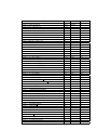
Space Impact - Project Report,
Design of Embedded Systems Advanced Course,
EDA385
Anton Norell - [email protected]
Erik Nilsson - [email protected]
Louise Hauzenberger - [email protected]
October 24, 2014
1
Abstract
Designing and implementing an arcade style space-shooter video game
using the retro cell phone game ‘Space Impact’ as inspiration. The game
were designed with hardware accelerated graphics output through VGA.
The player controls the game with a standard keyboard connected to the
USB-port of the Digilent Nexys 3 FPGA board. The project resulted in
a functional game that integrates both hardware and software in order to
display graphics and handle game logic.
2
Contents
1 Introduction
1.1 Tools and software used in this project . . . . . . . . . . . .
2 Architecture
2.1 Hardware . . . . . . . . .
2.1.1 CPU . . . . . . . .
2.1.2 PS/2 controller . .
2.1.3 GPU . . . . . . . .
2.1.4 Binary2BCD . . .
2.1.5 Memory . . . . . .
2.1.6 Device occupancy
2.2 Power Estimation . . . . .
2.3 Software . . . . . . . . . .
2.3.1 Registers . . . . .
.
.
.
.
.
.
.
.
.
.
.
.
.
.
.
.
.
.
.
.
.
.
.
.
.
.
.
.
.
.
.
.
.
.
.
.
.
.
.
.
.
.
.
.
.
.
.
.
.
.
.
.
.
.
.
.
.
.
.
.
.
.
.
.
.
.
.
.
.
.
.
.
.
.
.
.
.
.
.
.
.
.
.
.
.
.
.
.
.
.
.
.
.
.
.
.
.
.
.
.
.
.
.
.
.
.
.
.
.
.
.
.
.
.
.
.
.
.
.
.
.
.
.
.
.
.
.
.
.
.
.
.
.
.
.
.
.
.
.
.
.
.
.
.
.
.
.
.
.
.
.
.
.
.
.
.
.
.
.
.
.
.
.
.
.
.
.
.
.
.
.
.
.
.
.
.
.
.
.
.
4
4
4
. 5
. 5
. 6
. 6
. 8
. 8
. 8
. 9
. 10
. 10
3 User manual
11
3.1 Game objective . . . . . . . . . . . . . . . . . . . . . . . . . 11
3.2 Loading the game to the Nexys3 board . . . . . . . . . . . . 11
4 Problems encountered
12
4.1 AXI or PLB? . . . . . . . . . . . . . . . . . . . . . . . . . . 12
4.2 Unstable software . . . . . . . . . . . . . . . . . . . . . . . . 12
5 Conclusions and Result
12
5.1 Improvements . . . . . . . . . . . . . . . . . . . . . . . . . . 12
6 Contributions
13
7 References
14
8 Appendix A
15
3
Figure 1: Our inspiration, the classic mobile game Space Impact
1
Introduction
The purpose of this project is to design and implement an arcade style
video game similar to the old mobile phone game ‘Space Impact’, but with
a color enhanced graphics engine. The player controls the game with a
standard USB keyboard connected to the Digilent Nexys 3 FPGA board.
The game objective is to eliminate enemies that appears from the right
side of the screen. If the player gets hit by enemy fire or if the enemy moves
past the player the life-counter is decreased by one. When all lives are
depleted the game is over.
1.1
Tools and software used in this project
These are the software tools used in the development of this project:
• Xilinx Platform Studio 14.2
• ISE Project Navigator 14.2
• Xilinx Software Development Kit
• Digilent Adept 2.4.2
The project were developed at LTH in the autumn of 2014 using the
faculties computers running Windows 7 x64.
2
Architecture
This section describes the overall architecture of the game, including both
hardware and software.
4
Figure 2: An overview of our hardware architecture
2.1
Hardware
The hardware consists of the Microblaze CPU, memory, PS/2 controller
and the GPU. The GPU performs all drawing to the VGA monitor and is
the only hardware module that were designed from the ground up. The
other hardware modules were instantiated from IP-logic provided by the
Xilinx development tools.
All hardware will be implemented on the Nexys3 Spartan-6 FPGA
Board[1] from Digilent. Some of the hardware specifications includes:
• Xilinx Spartan6 XC6LX16-CS324
• Digilent Adept USB port for power, programming & data transfers
• USB-UART
• Type-A USB host for mouse, keyboard or memory stick
• 8-bit VGA
• 100MHz fixed-frequency oscillator
• 8 slide switches, 5 push buttons, 4-digit 7seg display, 8 LEDs
The board were provided by the course responsible teacher for this course.
Up to two boards were available per group which made testing very convenient.
2.1.1
CPU
The Microblaze is a soft core CPU designed by Xilinx for use as an IP
(Intellectual Property) core in user designs. It is 32-bits with both big
5
and little endianness. In this project one Microblaze CPU were used to
handle the game logic written in C.
2.1.2
PS/2 controller
The Nexys 3 development board has no actual PS/2 connector onboard
but still provides support of the PS/2 protocol via the USB host controller[2]. The PS/2 controller is a predefined component in Xilinx Platform Studio. It is a PLB (Processor Local Bus) slave which uses simple
state machines and shift registers to buffer the scancodes from the keyboard. The keyboard sends repeatable scancodes to the controller when a
key is pressed, when it is released the scancode 0xF0 are sent followed by
the key scancode. To connect the PS/2 controller to the rest of the project
which is connected through an AXI (Advanced eXtensible Interface) bus
a PLB to AXI bridge are used. The controller can be used in polling
mode or interrupt driven mode. In this project interrupt driven mode
was chosen to increase performance in software. The interrupts from the
PS/2 controller are connected to the AXI interrupt controller.
2.1.3
GPU
The GPU (Graphics Processing Unit) is the main self-developed hardware
unit developed by the team. It handles all drawing to the VGA monitor.
The GPU itself is divided into three main components:
• VGA controller
• Background generator
• Foreground generator
Figure 3: An blackbox overview of our vga accelerator
The VGA controller updates the screen with a frequency of 60Hz at
a resolution of 640x480 pixels. It is driven by a 25 MHz clock. This
module is very commonly implemented and was provided in whole by
Ulrich Zoltán from Digilent[3].
The Background generator is responsible for drawing the background
of the game. The background includes the score and lives text, top and
bottom borders, background stars and also moving stars in order to give
6
the appearance of forward movement to the player. At the end of the
project we decided to skip the stars that were not moving in order to give
the player a more accurate impression of forward movement.
Figure 4: An greybox overview of our vga accelerator
The Foreground generators responsibility is to draw the player and
enemy objects, projectiles, and the actual score and lives digits.
In order to draw a certain object, the generators look at the horizontal
(HS) and the vertical (VS) counters provided by the VGA controller to
determine if we are about to draw a pixel that is inside the object tile.
HS and VS checks against a number of conditions which takes the coordinates from the software registers into consideration to know what kind
of object we are about to draw, or if we are simply supposed to draw the
background. When it knows what object to draw, it uses lookup tables
(LUT) to draw a correct image of the object. The LUT is simply a matrix consisting of binary numbers that represents the monochrome image.
Using the vertical and horizontal counters and certain offsets related to
the object we can access the correct element in the LUT.
All modules are tied together in the vga top module where a process is
defined in order to determine if the foreground or the background should
be drawn to the monitor.
In order to avoid having to implement a SDRAM controller for the
external RAM on the Nexys3 board, all graphics are stored in the FPGAs
block RAM (BRAM). Since the game have relatively simple graphics this
should cause no major problems. The graphics for the player, enemies,
score, lives and projectiles are stored as binary values in std logic vectors
forming a matrix.
7
2.1.4
Binary2BCD
Figure 5: The visual elements of the game are stored as matrices for easy access.
Numbers are drawn one by one, that way only the graphics for 0 to 9
needs to be stored. The binary2BCD component uses the shift and add
3 algorithm which takes an 8-bit number and separates every digit to 4
bits each, giving an output of 12 bits. An 8-bit number ranges from 0 to
255 which is a too small number for our intended score range, hence the
score is stored in two halves of 8 bit each. That way it is possible to show
score up to 9999.
2.1.5
Memory
As mentioned before, no external memory was used in this project. All
graphics are stored in the onboard block RAM of the FPGA. In a more
advanced game this would probably not be feasible since the onboard
RAM is relatively limited.
2.1.6
Device occupancy
For a complete listing of the FPGA utilization, see appendix A.
8
Figure 6: An overview of the hardware architecture in Xilinx Platform Studio.
2.2
Power Estimation
Xilinx XPower Analyzer was used to analyze the power of the GPU design.
Figure 7: Power analysis of the design.
9
2.3
Software
The software of the game is running on the Microblaze CPU implemented
on the FPGA. The responsibility of the software is to handle the game
logic, including keeping track of scores and lives, collision detection, generating of enemies and moving the player.
The software are divided in two parts, the main program and the
interrupt handler. In every iteration of the main program it runs a collision
detection and calculates a new position for all the enemies and bullets. If
anything is changed it is sent to the right register.
The interrupt handler where implemented to take care of interrupts.
When the keyboard sends an interrupt the handlers execution are triggered which listens to the scancodes corresponding to W, S, P, SPACE
BAR and ESC. Depending on the scancode different things should happen; S and W moves the ship up and down, P pauses the game, SPACE
BAR fires and ESC resets the game. When the handler has taken care of
the interrupt the main program will continue its execution.
2.3.1
Registers
Figure 8: A drawing of the bit distribution in the registers.
Ten hardware registers for saving object positions, score and lives were
instantiated at the beginning of the project. Because of the low complexity
of the game, we figured that ten registers would be enough. Each register
is utilized to make use of as many bits as possible in order not to waste
any resources.
10
3
3.1
User manual
Game objective
The goal of the game is to stay alive as long as possible by not getting hit
by any enemy ships or letting any enemies get past the player. Eliminating
enemies generates score that eventually adds to the life counter. Failure
to eliminate all enemies on screen or getting hit results in a subtraction
from the life counter. When all lives are depleted the game is over. The
controls are simple, W moves the player up, S moves the player down and
SPACE BAR is used to fire a projectile. P pauses the game and ESC
resets it.
3.2
Loading the game to the Nexys3 board
Launch the Digilent Adept software and browse for the download.bit file in
the uncompressed . . . \game logic\space impact axi hw platform folder.
Press Program to load the bit file into the FPGA.
Figure 9: Digilent Adept for Nexys3.
11
4
Problems encountered
As with all projects, unforeseen problems often occurs. So was the case
even in this project. This holds particularly true for the keyboard controller which were supposed to take only a week to get operational. In
reality it took about three weeks.
4.1
AXI or PLB?
The choice of system bus had to be made at the start of the project.
Initially the choice stood between AXI and PLB.
AXI was first chosen since it was the most recent on-chip interconnect.
It did however not provide any support for the PS/2 controller IP available
in Xilinx Platform Studio. Using only a PLB bus made it difficult to
synthesize the design due to too many bonded IOBs. This made us decide
to use a PLB to AXI bridge to connect the PS/2 controller to the AXI
bus.
4.2
Unstable software
The seemingly unstable development software caused some frustration
during the course of this project. Sometimes when adding new ports to
the hardware logic or trying to connect a module to a bus in the Xilinx
Platform Studio the software would crash inexplicably. When we finally
got all modules connected properly we decided to never touch the connections again if not absolutely necessary. It was also frustrating to have
to generate a new netlist and bitstream every time the hardware modules
were changed.
5
Conclusions and Result
The project resulted in a functional arcade style game with basic controls and a classic game mode. As a learning experience the project was
very rewarding. None of the team members had any previous experience of computer graphics. By the end of the project all members of the
team could agree that it is sometimes difficult to estimate what parts of
a project is most time consuming. This holds particularly true for the
keyboard controller that were only supposed to take a fraction of the actual implementation time. Debugging hardware proved to be quite time
consuming as well, this is definitely something to keep in mind in future
hardware related projects.
5.1
Improvements
Due to a somewhat pressed time schedule, many features that could have
improved gameplay had to be omitted. These features include but are not
limited to:
• A variety of levels available to the player
• Better enemy intelligence
12
Figure 10: A view over our setup and the final look of the game.
• Full eight-direction movement
• Sound effects and music
• Improved graphics and animations
Many of these features were unrealistic to implement in such a short
time span due to the team’s inexperience with computer graphics. However, features like the ones presented above seems less unrealistic in future
projects because of our newly acquired experiences.
6
Contributions
This section list the individual contributions of the team members of this
project.
Anton - GPU, Software, Report
Erik - GPU, Artwork, Report
Louise - PS/2 controller, Binary2BCD, Software, Report
We drew inspiration from a previous project, namely AirCombat.
13
7
References
[1] Digilent Inc. - Digital Design Engineer’s Source:
http://www.digilentinc.com/ProductsDetail.cfm?NavPath=2,400,897&ProdN̄EXYS3
Fetched 2014-10-12
[2] Nexys3 rm V2 http://www.digilentinc.com/Data/Products/NEXYS3/Nexys3 rm V2.pdf
Fetched 2014-10-12
[3] http://ece.wpi.edu/˜rjduck/vga controller 640 60.vhd Fetched 201410-12
14
8
Appendix A
15
Device Utilization Summary
Slice Logic Utilization
Number of Slice Registers
Number used as Flip Flops
Number used as Latches
Number used as Latch-thrus
Number used as AND/OR logics
Number of Slice LUTs
Number used as logic
Number using O6 output only
Number using O5 output only
Number using O5 and O6
Number used as ROM
Number used as Memory
Number used exclusively as route-thrus
Number with same-slice register load
Number with same-slice carry load
Number with other load
Number of occupied Slices
Nummber of MUXCYs used
Number of LUT Flip Flop pairs used
Number with an unused Flip Flop
Number with an unused LUT
Number of fully used LUT-FF pairs
Number of unique control sets
Number of slice register sites lost to control set restrictions
Number of bonded IOBs
Number of RAMB16BWERs
Number of RAMB8BWERs
Number of BUFIO2/BUFIO2 2CLKs
Number of BUFIO2FB/BUFIO2FB 2CLKs
Number of BUFG/BUFGMUXs
Number used as BUFGs
Number used as BUFGMUX
Number of DCM/DCM CLKGENs
Number of ILOGIC2/ISERDES2s
Number of IODELAY2/IODRP2/IODRP2 MCBs
Number of OLOGIC2/OSERDES2s
Number of BSCANs
Number of BUFHs
Number of BUFPLLs
Number of BUFPLL MCBs
Number of DSP48A1s
Number of ICAPs
Number of MCBs
Number of PCILOGICSEs
Number of PLL ADVs
16
Number of PMVs
Number of STARTUPs
Number of SUSPEND SYNCs
Average Fanout of Non-Clock Nets
Used
864
864
0
0
0
1,887
1,879
1,219
0
660
0
0
8
8
0
0
777
656
2,179
1,381
292
506
33
128
99
0
0
0
0
2
2
0
0
0
0
0
0
0
0
0
0
0
0
0
0
0
0
0
4.44
Available
18,224
Utilization
4%
9,112
9,112
20%
20%
2,176
0%
2,278
4,556
34%
14%
2,179
2,179
2,179
63%
13%
23%
18,224
232
32
64
32
32
16
1%
42%
0%
0%
0%
0%
12%
4
248
248
248
4
128
8
4
32
1
2
2
2
1
1
1
0%
0%
0%
0%
0%
0%
0%
0%
0%
0%
0%
0%
0%
0%
0%
0%