1
INTERFACING WITH EXTERNAL MEMORY
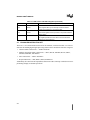
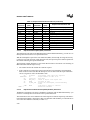
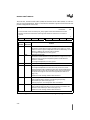
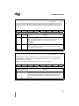
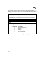
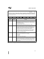
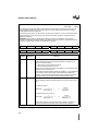
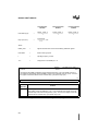
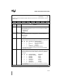
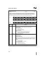
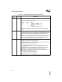
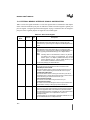
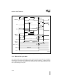
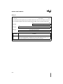
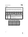
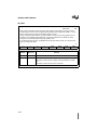
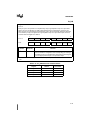
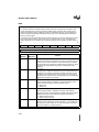
Address:
Reset State:
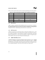
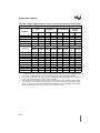
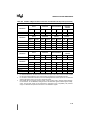
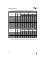
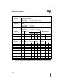
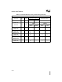
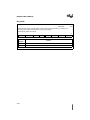
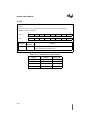
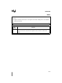
BUSCONx (Continued)
x = 0–5
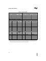
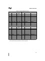
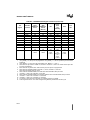
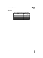
Table 13-3 on page 13-5
(x = 0) 0FH
(x = 1–5) 00H
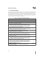
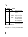
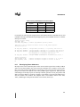
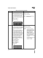
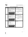
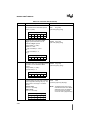
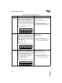
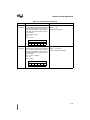
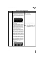
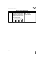
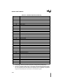
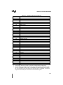
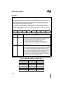
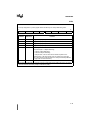
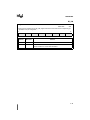
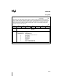
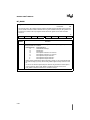
For the address range assigned to chip-select x, the bus control (BUSCONx) register specifies the
number of wait states, the bus width, and the address/data multiplexing for all external bus cycles that
access address range x. BUSCONx also determines whether chip-select output x will be activated
when the address region for chip select x+1 is accessed. This option makes accessing a memory
device using two different bus configurations possible.
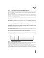
The chip-select output signals share package pins with port 3. Use the port registers to configure these
pins as general-purpose I/O signals or as chip-select signals (see “Chip-select Signals (Port 3)” on
page 7-8). The bus configuration programmed in BUSCONx applies to address range x, regardless of
the port 3 pin configurations.
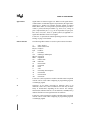
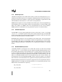
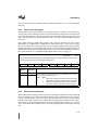
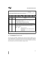
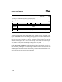
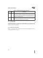
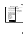
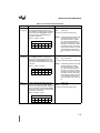
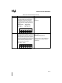
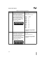
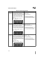
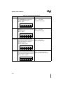
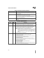
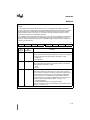
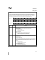
7
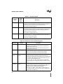
DEMUX
Bit
Number
4
0
BW16
REMAP
WRWS
WS3
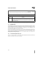
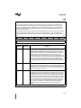
Bit
Mnemonic
WRWS
WS2
WS1
WS0
Function
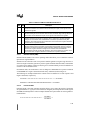
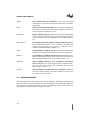
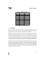
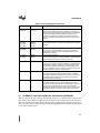
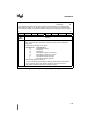
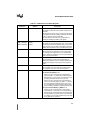
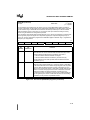
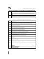
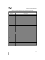
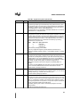
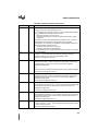
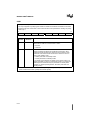
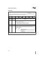
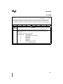
Write Operation Wait State
When this bit is set, the bus controller adds one state time (2t) to write
operations within the address region specified by chip select x.
0 = data and address hold time remains unchanged
1 = data and address hold time increases by one state time (2t)
See the datasheet for the write operation data and address hold time
specification (TWHAX).
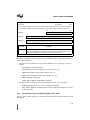
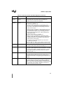
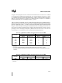
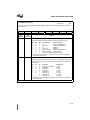
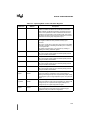
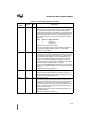
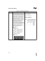
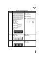
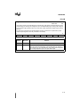
3:0
WS3:0
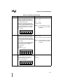
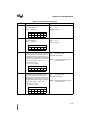
Wait States
These bits, along with the READY pin, control the number of wait states
for all external accesses to the address range assigned to the chip-select
x channel. Write the desired minimum number of wait states (0–15) to
WS3:0. If the programmed number of wait states is greater than zero and
READY is low when this programmed number of wait states is reached,
additional wait states are added until READY is pulled high. If the
programmed number of wait states is equal to zero, hold the READY pin
high. Programming the number of wait states equal to zero and holding
the READY pin low produces unpredictable results.
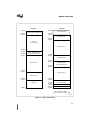
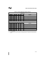
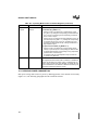
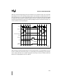
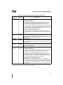
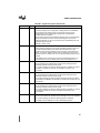
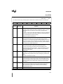
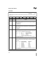
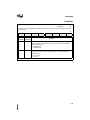
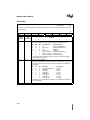
Figure 13-4. Bus Control (BUSCONx) Registers (Continued)
13-13