1
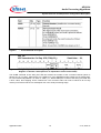
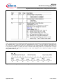
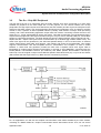
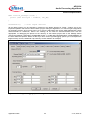
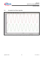
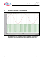
Application Note, V1.0, Jan. 2007 AP16104 XC161CJ Performing Audio Processing by means of the XC161CJ This application note explains how to perform advanced processing on audio signals with well known algorithms, ranging from extremely simple to computation-intensive ones. Management of On-Chip Peripherals, coming into play for audio signal acquisition, is also illustrated with reference to the embedded microcontrollers of the Infineon XC166 Family Microcontrollers Edition 2007-02-19 Published by Infineon Technologies AG 81726 München, Germany © Infineon Technologies AG 2007. All Rights Reserved. LEGAL DISCLAIMER THE INFORMATION GIVEN IN THIS APPLICATION NOTE IS GIVEN AS A HINT FOR THE IMPLEMENTATION OF THE INFINEON TECHNOLOGIES COMPONENT ONLY AND SHALL NOT BE REGARDED AS ANY DESCRIPTION OR WARRANTY OF A CERTAIN FUNCTIONALITY, CONDITION OR QUALITY OF THE INFINEON TECHNOLOGIES COMPONENT. THE RECIPIENT OF THIS APPLICATION NOTE MUST VERIFY ANY FUNCTION DESCRIBED HEREIN IN THE REAL APPLICATION. INFINEON TECHNOLOGIES HEREBY DISCLAIMS ANY AND ALL WARRANTIES AND LIABILITIES OF ANY KIND (INCLUDING WITHOUT LIMITATION WARRANTIES OF NON-INFRINGEMENT OF INTELLECTUAL PROPERTY RIGHTS OF ANY THIRD PARTY) WITH RESPECT TO ANY AND ALL INFORMATION GIVEN IN THIS APPLICATION NOTE. Information For further information on technology, delivery terms and conditions and prices please contact your nearest Infineon Technologies Office (www.infineon.com). Warnings Due to technical requirements components may contain dangerous substances. For information on the types in question please contact your nearest Infineon Technologies Office. Infineon Technologies Components may only be used in life-support devices or systems with the express written approval of Infineon Technologies, if a failure of such components can reasonably be expected to cause the failure of that life-support device or system, or to affect the safety or effectiveness of that device or system. Life support devices or systems are intended to be implanted in the human body, or to support and/or maintain and sustain and/or protect human life. If they fail, it is reasonable to assume that the health of the user or other persons may be endangered. AP16104 Audio Processing Algorithms AP16104 Revision History: 2007-01 Previous Version: none Page V1.0 Subjects (major changes since last revision) We Listen to Your Comments Any information within this document that you feel is wrong, unclear or missing at all? Your feedback will help us to continuously improve the quality of this document. Please send your proposal (including a reference to this document) to: [email protected] Application Note 3 V1.0, 2007-01 AP16104 Audio Processing Algorithms Table of Contents Page 1 Abstract..........................................................................................................................................5 2 Audio Processing Algorithms......................................................................................................6 3 3.1 3.2 3.3 3.4 System Overview and Peripherals Configuration Description.................................................7 The On – Chip ADC Peripheral.......................................................................................................8 The On – Chip timer in CAPCOM Unit Peripheral ........................................................................13 The On – Chip SSC Peripheral .....................................................................................................16 2 The On – Chip I C Bus Module.....................................................................................................21 4 4.1 4.2 4.2.1 4.2.1.1 4.2.1.2 4.2.1.3 4.2.1.4 Software Implementation ...........................................................................................................29 Developing the Code.....................................................................................................................29 Wanna Debug? .............................................................................................................................30 2 I C Codes from Master Generator ................................................................................................38 Distortion Algorithm Bytecodes .....................................................................................................38 Noise Gate Algorithm Bytecodes ..................................................................................................38 Phaser Algorithm Bytecodes.........................................................................................................38 Flanger – Chorus Algorithm Bytecodes ........................................................................................38 5 5.1 5.2 5.3 5.4 Code Execution and How to make it run for real .....................................................................40 The Bootstrap Loader Mode .........................................................................................................40 OCDS Cerberus On-Chip Module.................................................................................................44 Programming the On – Chip Flash................................................................................................46 Hardware connections ..................................................................................................................49 6 6.1 6.2 6.3 6.4 Simulation Results ......................................................................................................................58 Screenshot from Distortion algorithm............................................................................................58 Screenshot from Noise Gate algorithm .........................................................................................59 Screenshot from Phaser algorithm ...............................................................................................60 Screenshot from Flanger – Chorus algorithm ...............................................................................61 7 Further Improvements and Conclusions..................................................................................62 8 Glossary .......................................................................................................................................63 9 Literature......................................................................................................................................64 Application Note 4 V1.0, 2007-01 AP16104 Audio Processing Algorithms Abstract 1 Abstract The Infineon 16-bit Microcontrollers are suitable for an extended range of applications, from Automotive and Data logging, all the way to the driving stage of a DC brushless motor. This application note addresses a particular market sector which has significantly evolved in the last 10 years, due to the improvements of processing power and peripheral performance of electron devices (e.g., DSPs, ADCs): audio processing. Audio processing is a branch of the acoustic science, which studies the implementation of algorithms to improve or drastically change the contents of an audio signal. The most common examples of audio processing include audio encoding and decoding and the application of sound effects to the baseline audio signal. A number of editing tools have been developed for this purpose. However, the most challenging aspect of audio processing is represented by the execution of processing algorithms in real-time on mobile terminals, which are generally referred to as “embedded computing”. Mobile terminals are resourceconstrained systems featuring tight power budgets; therefore the performance of low power multimedia platforms has to be pushed to the limit while operating in an energy-efficient fashion. Interestingly, technology advances are leading to the implementation of complex systems onto the same silicon die, thus making the so-called “Systems-on-Chip” available on the market. Following this trend, low-end Infineon microcontrollers consist of the integration of a DSP, several embedded memory banks and of a number of I/O peripherals on the same chip. This system natively targets automotive applications, however its deployment for audio processing is an interesting new application frontier, since multimedia contents are gaining momentum also in the automotive domain. This application note illustrates how we can use a simple 16 bit Microcontroller and morph it into an Audio Processor. We used the 16-bit XC161CJ – 16F Microcontroller, although all applications presented here are suitable also for the XC164CS/XC164CM Series and XC167CI. Application Note 5 V1.0, 2007-01 AP16104 Audio Processing Algorithms Audio Processing Algorithms 2 Audio Processing Algorithms The audio processing algorithms implemented in this application note are: • • • • Distortion Unit (Distortion.c): distortion is the effect obtained by increasing the range of the signal, so that the non-linearities of the amplifier are stimulated resulting in clipping of the signal peaks and in an enhancement of the signal spectrum with odd and even harmonics. From a listening viewpoint, the output signal sounds like a “rough”, metallic sound, which is completely different from the original signal fed into the amplifier. In the presented case study, the XC161 unit plays the role of the “amplifier”, performing gain level adjustment based on user specifications. The “tuning knobs” made available to the user are the Gain Level and the final Volume Level of the audio signal. Noise Gate (Gate.c): noise gating is a common procedure in audio processing, when mixing different tracks of music sources and especially when working in noisy environments (i.e., overdriven amplifiers). The goal of the gating procedure is to attenuate or even eliminate audio signals whose intensity overpasses a pre-defined threshold. When I/O characteristics of an audio signal are plotted and the threshold is established (in this application note, it is fixed to -20 dB), every single time the signal crosses the threshold it gets attenuated by a predefined ratio, which can be adjusted by the end-user by means of the Decay and Rate parameters. Phaser (Phaser.c): the Phaser, as the name itself suggests, is an algorithm that receives as an input a pure audio signal and outputs the sum of a phased out signal (achieved by filtering the audio signal in multiple stages) and the original signal. This results in the characteristic “swirling” sound of the ’70s songs, when the audio seems to periodically change from a speaker to another. User can change parameters like sweep rate of the filters, mix of original and processed signals (called dry and wet), delay of filtering and feedback ratio. Flanger – Chorus (FlaCho.c): The flanger-chorus effect reproduces what happens when two people play instruments in unison. They are not always playing in precise synchronization, so there is some delay between the sounds they produce. In addition, the pitch of the two instruments can deviate somewhat, despite careful tuning. In practice, the flanger-chorus effect has been implemented by summing the original unprocessed signal with a delayed version. The delay line is actually a variable length delay line, i.e. the delay time changes over time. To understand how the pitch is changed, picture the delay as a recording device. It is storing an exact copy of the input signal as it arrives, much like a cassette recorder, and it then outputs that a little bit later, at the same rate. To increase the amount of delay, you need a longer segment of the signal to be stored in the delay line before it is played back. To do this, you may want to read out of the delay line at a slower rate than it is being written (the recording rate is unchanged, so more of the signal is being stored). So, by mixing this delayed and pitch-modulated copy of the input signal together with the original signal, we get the chorus effect. In general, some periodic waveform, such as a sine wave, is used to actually change the delay time. This waveform changes slowly (say 3 Hz and below) and is referred to as a Low Frequency Oscillator. In this application note, we however made us of a triangular waveform instead of the sine wave. With respect to a pure chorus effect, this implementation adds a feedback path from the output of the algorithm to its input, which is typical of the flanger effect. Users can change parameters like LFO peak-to-peak amplitude, LFO frequency, the Feedback ratio and of course the level of wet & dry signals. All these algorithms were coded in the Embedded C programming language. The interested reader can find more information on algorithm kernels and their implementation in real-life commercial systems at the following web page: http://www.harmony-central.com. Application Note 6 V1.0, 2007-01 AP16104 Audio Processing Algorithms System Overview and Peripherals Configuration Description 3 System Overview and Peripherals Configuration Description The implementation of these algorithms on the XC161 microcontroller consists of a typical signal acquisition and DSP processing chain. At first, the analog audio input signal is sampled and translated into digital form. A timer is used to track the analog-to-digital conversion process to the desired sampling period. The embedded microcontroller was used to execute the audio processing algorithms and finally a serial link was deployed to feed an off-chip digital-to-analog conversion, before the audio playback stage. The schematic architecture of the audio processing system, centered on the XC161 embedded microcontroller can be resumed like this: the sampling and quantization stages are performed by the on-chip ADC module of the Infineon device, the ADC is programmed to work on interrupts raised by the synchronization CAPCOM/Timer on-chip module. The DSP core of the XC161 is programmed in embedded C language, coding the above defined audio processing algorithms. The serial output of processed data is performed through the on-chip High Speed Synchronous Serial Port (standard-SPI compatible) SSC that could be interchanged, for a particular case, with on-chip Asynchronous/Synchronous Serial Port ASC (i.e. when you don’t have a DAC device or you want to implement a kind of “Real – Time Debugging” using the Terminal Program). We must also consider that a processing system must include user tunable controls, so for example if we want to set the volume of the audio output, the system must provide a knob or control for that functionality. IIC bus compliant controls are implemented in this application note for the entire management of the algorithms parameters like: volume, gain, threshold gate, etc… For correct operation, all these peripherals have to be programmed by means of the Special Function Registers (SFRs) or Extended Special Function Registers (ESFRs) associated to each of them. An in-depth overview of the implementation details (including peripheral settings) is the focus of next sections. In order to maintain the compatibility of the coded above algorithms presented in this application note, with the world audio standards, we adopted a raw data representation that follow the Wave Format PCM (Pulse Coded Modulation) as the reference audio coding format, since it is used in 80% of audio processing systems, but not using the RIFF (stands for Resource Interchange File Format) header and the format subchunks (more information about this on http://ccrma.stanford.edu/CCRMA/Courses/422/projects/WaveFormat/). The representation of an audio signal with this codification method is pretty straightforward and doesn’t need external tool like an encoder/decoder (as used in the standard Motion Picture Expert Group – Layer 3), since the information resides on a waveform. Another important characteristic of the PCM is the lossless codification of the data, so this means that the Power Spectral Density of the native audio signal stays the same after the codification 1 process . The representation of the data strictly depends by the bit depth used for the quantization stage so: Bit Depth from 1 to 15 bit This bit depth define that all the sampled values from the input audio signal are stored as unsigned bytes ( ) ranging from the quantization levels between 0 and 2 − 1 . The standard is the 8 bit quantization depth and this topology of data characterization is so called “Offset Wave”, justified by the fact that the mean value of a coded audio waveform is not null. bit _ depth _ used Bit Depth more than 16 bit Using this quantization steps all the sampled values are stored as 2's-complement signed integers, ranging from ( ) 2 bit _ depth _ used − 2 bit _ depth _ used to 2 2 − 1 . This is not an “Offset Wave” representation as you can see with a 16 bit depth, all the sampled data goes from -32768 to 32767 passing by the null mean value. Using the Infineon Technologies XC161 microcontroller with the On – Chip ADC Peripheral we’ve chosen to develop the algorithms with a bit depth of 8, marking a good trade off between audio quality of the output data and computation speed. 1 Remember that we’re going to work with signals with a baseband from 20 Hz to 20KHz (good human ear perception) Application Note 7 V1.0, 2007-01 AP16104 Audio Processing Algorithms System Overview and Peripherals Configuration Description 3.1 The On – Chip ADC Peripheral The On – Chip Analog-to-Digital Converter is a key module for the whole application. The Infineon XC161CJ provides an on-chip Analog-to-Digital converter with a software selectable resolution of 8 bit or 10 bit and an internal sample and hold circuitry. An input multiplexer selects between up to 12 analog input channels (alternate functions of Port 5) either via software (fixed channel modes) or automatically (auto scan modes). We chose a quantization depth of 8 bits as said above. Watch out that the Analog Input Port channels from AN15 through AN0 are alternate functions of Port 5, which is an input-only port. The Port 5 lines may either be used as analog or digital inputs. For pins that shall be used as analog inputs it is recommended to disable the digital input stage via register P5DIDIS. This avoids undesired cross currents and switching noise while the (analog) input signal level is between VIL and VIH. The functions of the A/D converter are controlled by two sets of bit-addressable control registers. In compatibility mode, registers ADC_CON and ADC_CON1 are used, in enhanced mode, registers ADC_CTR0, ADC_CTR2, and ADC_CTR2IN are used. Their bitfields specify the analog channel to be acted upon, the conversion mode, and also reflect the status of the converter. Different conversion schemes are made available by the ADC, but for this particular application we opted for the Fixed Channel Single Conversion Mode, that produces only one conversion result per ADC channel. This choice might be counterintuitive, since a Fixed Channel Continuous Conversion Mode is also available, that produces continuous conversions and repeatedly restores the conversion results in the result register. The reason behind this lies in sample rate considerations. In Audio Processing, a set of standard sample rates ranging from 8 to 192 KHz must be used, in order to guarantee the portability of the written code over different systems but we decided to use the standard rate used on the PCM highways used in wireless standard communication (GSM, EDGE, Bluetooth, etc.) as 8 KHz in order to provide a bitrate of 64 Kbps. By using the Fixed Channel Continuous Conversion Mode, we cannot have a control over the sample rate, but we are forced to use the rate value super-imposed by the microcontroller vendor, which can be varied from a set of predetermined values for the XC161CJ chip. In this case, the sampling time will be calculated as follows: • • • Assumptions: fADC = 40 MHz (i.e. tADC = 25), ADCTC = 01B, ADSTC = 00B Basic Clock: fBC = fADC/2 = 20 MHz, i.e., tBC = 50 ns Sampling time: ts = tBC * 8 = 400 ns Which gives a sample rate of 2,5 MHz (too much for our needs). The time for a complete conversion includes not only the sample time, but the conversion time itself (successive approximation and calibration since the ADC is a SAR type), and the time required to transfer the digital value to the result register, as shown in the example below: • • With Post – Calibration: tC8P = tS + 44 × tBC + 6 × tADC = (2200 + 400 + 150) ns = 2.75 µs Without Post – Calibration: tC8 = tS + 32 × tBC + 6 × tADC = (1600 + 400 + 150) ns = 2.15 µs The ADCTC and ADSTC binary values are bit-fields of the SFR ADC_CON that control the configuration of the ADC On – Chip Module, the same SFR that we will program now for our applications. We mentioned our intention to use a quantization resolution of 8 bits, while having full control on the sample rate. This involves programming two particular SFRs dedicated to the ADC module configuration: the ADC_CON and the ADC_CON1. Application Note 8 V1.0, 2007-01 AP16104 Audio Processing Algorithms System Overview and Peripherals Configuration Description Figure 1 ADC_CON Register with Bitfields description from 15 to 10 Figure 2 ADC_CON Register with Bitfields description from 9 to 0 Application Note 9 V1.0, 2007-01 AP16104 Audio Processing Algorithms System Overview and Peripherals Configuration Description The ADCH field selects the multiplexed A/D channel we want to use, which is channel 0 in our case (corresponding to the PORT5.0 AN0 pin of the Infineon XC161CJ Chip), so the value of this 4-bit field will be 0000B. ADM selects the conversion scheme and we want to use the Fixed Channel Single Conversion Mode that corresponds to setting the 2-bit field to 00B value. All the other fields do not have to be touched for the configuration phase, so everything will be set to 0B. The most critical field to be set to meet our specifications is ADCTC. For it, we set a value of 01B , thus instructing the ADC module to grant conversion at fADC/2 that combined with a maximum sample time of tBCx 8, gives a maximum conversion time in the order of µs (which is good for us). Under these assumptions, The ADC_CON hexadecimal configuration value will be 4000H. Figure 3 ADC_CON1 Register with Bitfields description from 15 to 13 Application Note 10 V1.0, 2007-01 AP16104 Audio Processing Algorithms System Overview and Peripherals Configuration Description Figure 4 ADC_CON1 Register with Bitfields description from 12 to 0 In the ADC_CON1 register, the only field we have to set in the configuration phase is RES to 1B , thus instructing the ADC module to work with 8 – bit data resolution. If we use the Keil Compiler, we can simply act on the value of this bit by setting the SFR bit variable type ADC_CON1_RES to 1. This completes the configuration phase of the ADC converter and opens up the next issue: how can we read the input samples? When an analog signal is fed to a channel of the ADC on-chip Module (e.g., PORT5.0 AN0), the conversion into digital form is performed by setting a bit in the register ADC_CON which is equivalent to a conversion start command. This is the ADST bit (accessible with Keil Compiler by setting the SFR bit variable type ADC_CON_ADST). When a complete conversion has occurred, the result of the conversion will be placed into the result register ADC_DAT and the interrupt flag ADC_IR will be set into another SFR named ADC_CIC, which indicates conversion completion and raises an interrupt. Figure 5 ADC_DAT Special Function Register… Application Note 11 V1.0, 2007-01 AP16104 Audio Processing Algorithms System Overview and Peripherals Configuration Description Figure 6 … and its Bitfields description Figure 7 ADC_CIC Special Function Register (please refer to the general Interrupt Control Register on XC161CJ description for an explanation of the control fields) The CHNR 4-bit field of the ADC_DAT SFR will contain the number of the converted channel (which is always zero in our case), while the bit 9 to 2 (MSB is 9) of the ADRES field will contain the converted value. For correct data interpretation, we have to “mask” (i.e., bitwise AND) the content of the ADC_DAT SFR with a 3FCH value, thus stripping off the useless bits. The converted value can now be stored to an on-chip memory unit of the XC161CJ for subsequent use in the audio processing stage. Application Note 12 V1.0, 2007-01 AP16104 Audio Processing Algorithms System Overview and Peripherals Configuration Description 3.2 The On – Chip timer in CAPCOM Unit Peripheral CAPCOM stays for CAPture and COMpare Unit and the XC161CJ Chip architecture includes two of them, interacting with timers. A CAPCOM channel can capture the contents of a timer on specific internal or external events, or it can compare a timer’s contents with given values, and modify output signals in case of a match. This is particularly useful in our applications, since the ADC sampling & conversion mechanism must be synchronized with a pre-defined standard rate compliant with the codification format. For the purpose of this application note, we exploit the functionality of this peripheral to COMpare the timer content with a defined value and to raise a timer interrupt when a match occurs. Now we have the global picture of the implementation of the audio acquisition stage. In fact, the ADC module performs a conversion when the bit ADST in register ADC_CON is set to 1B. Without a sampling time control triggered by CAPCOM timer interrupt, by placing this instruction inside the void main (void) of the application program, the ADC will perform a single conversion and go idle forever. If the instruction is placed within a while(1) loop, the ADC will perform continuous conversion, but not triggered by the Timer interrupt so it will be used the maximum sample rate and conversion rate set on the ADCTC-ADSTC fields of the ADC_CON SFR. The correct solution is to put the data conversion triggering instruction within a function that will be called at every interrupt raised by the timer. In turn, this interrupt is raised when the COMpare unit reaches a pre-determined value, thus enabling full control on the sampling process timings. Suppose that we want to perform audio processing at a sample rate of “samplerate” Hz, all we have to do is: define that the interrupt must be raised every time the timer has reached the value set into a macro definition that looks like this: #define T0_RELOAD ((unsigned int )(0-(CLOCK / samplerate))) and that allows the extraction of the value in seconds that must be counted before an interrupt is raised. Next, write a routine that responds to a “Reached counting value” interrupt code, and inside it, write the necessary code to start ADC conversion ADC_CON_ADST = 1) and process it. Programming the CAPCOM/Timer Unit is quite simple. We will force an operating condition named Stagger Mode, which means that the output signals are switched consecutively in 8 steps, which distributes the switching steps over a certain time. In staggered mode, the maximum resolution is 8 tCC. This operating mode is achieved by setting the bit STAG in the register CC1_IOC. The timer deputed to counting the time spent is Timer0. So, in the void main (void) of our application programs we have to set the timer control register CC1_T01CON with hexadecimal value 40H , meaning “start Timer 0”. Figure 8 The CC1_T01CON Special Function Register… Application Note 13 V1.0, 2007-01 AP16104 Audio Processing Algorithms System Overview and Peripherals Configuration Description Figure 9 …and its Bitfields description Then, we have to force an interrupt generation whenever the counting time is elapsed (the trap number 20H for CAPCOM Timer 0), and we instruct the CAPCOM/Timer Unit to do this by setting the dedicated SFR CC1_T0IC to an hexadecimal value of 44H (meaning to set the register bit field T0IE (Interrupt Enable) and ILVL (Interrupt Level) to 1). Finally we have to set the reload timing value to our (sample rate / CLOCK) requirement (with the XC161CJ we assume a chip clock frequency of 20 MHz), by setting the SFRs CC1_T0REL and CC1_T0. Figure 10 The CC1_M0 Special Function Register… Application Note 14 V1.0, 2007-01 AP16104 Audio Processing Algorithms System Overview and Peripherals Configuration Description Figure 11 …and its Bitfield description Figure 12 Table 17-2 from the XC161CJ Peripherals Manual on working modes for CAPCOM registers CCy We also have to program this SFR with hexadecimal value 7H to enable the compare mode for CC1_CC0 input. Application Note 15 V1.0, 2007-01 AP16104 Audio Processing Algorithms System Overview and Peripherals Configuration Description 3.3 The On – Chip SSC Peripheral The last step that has to be performed after the audio samples have been processed is to make them available for playback on the serial output link. For this purpose, we can choose between two on-chip peripherals: the High Speed Synchronous Serial Port (the SSC module) and the Asynchronous/Synchronous Serial Port (the ASC module). For all the algorithms described in this application note, we opted for the SSC module. In fact, it permits an SPI-compatible interface (a widely used solution in today’s audio processing market), and it also allows debug application output data even without connecting external devices to the serial port (i.e., a high speed Digital-to-Analog Converter). This latter functionality is accomplished through a simple terminal program like the HyperTerminal running on every PC and a classical COM port, and enables plotting of output data waveforms. The High-Speed Synchronous Serial Interface (SSC) supports both full – duplex and half – duplex serial synchronous communication up to 20 Mbit/s (@ 40 MHz module clock). The serial clock signal can be generated by the SSC itself (Master Mode) or can be received from an external master (Slave Mode). Data width, shift direction, clock polarity and phase are programmable. This module supports communication with SPI-compatible devices. Transmission and reception of data is double buffered. A 16-bit baud rate generator provides the SSC with a separate serial clock signal. Data is transmitted on module internal signal lines MTX/STX or received on lines MRX/SRX, connected with pins MTSR (Master Transmit/Slave Receive pin PORT3.9) and MRST (Master Receive/Slave Transmit pin PORT3.8). The clock signal is output via line MSCLK (Master Serial Shift Clock pin) or input via line SSCLK (Slave Serial Shift Clock pin PORT3.13). Both lines are connected to pin SCLK. Figure 13 An Overview of the SSC Block Diagram For our applications, we will use the simplest communication mode made available by the SSC module, consisting of a Master Mode full – duplex communication with a data width of 8 bits. Thus, we can set the Application Note 16 V1.0, 2007-01 AP16104 Audio Processing Algorithms System Overview and Peripherals Configuration Description clock to be sent to the external device connected to the SSC module (and the clock frequency will correspond to the sample rate used for sampling the analog input signal at the external device). In order to program the SSC module in this way, the only thing we have to do is to set the SFR SSC0_CON and SSC0_BR as explained next. Figure 14 SSC_xCON Register with Bitfields description from 15 to 7 in Programming Mode Application Note 17 V1.0, 2007-01 AP16104 Audio Processing Algorithms System Overview and Peripherals Configuration Description Figure 15 SSCx_CON Register with Bitfields description from 6 to 0 in Programming Mode and SSCx_CON Register with Bitfields description 15 and 14 in Operating Mode Application Note 18 V1.0, 2007-01 AP16104 Audio Processing Algorithms System Overview and Peripherals Configuration Description Figure 16 SSCx_CON Register with Bitfields description from 12 to 0 in Operating Mode During the module initialization we have to set the enable bit field of SSC0_CON SFR to 0B. The Master Select field must be set to 1B to make the SSC work as a Master and to generate the shift clock and output it via the SCLK pin (PORT 3.13). The 4-bit field BM must be set to 0111B, forcing a data width of 7 + 1 = 8 bits. Other fields must be set to 0B therefore the SSC0_CON SFR must be programmed with a hexadecimal value of 4007H. Once configured, SSC module operation will be invoked within the interrupt service routine. In fact, every time a data sample is processed, it has to be loaded into a special SFR named SSC0_TB (standing for Transmit Buffer) for output. This is the solution used to perform the real-time processing. It’s possible to interchange the use of SSC Port with ASC module for non-real-time processing, by simply deploying the ASC0_TB register instead of the SSC0_TB, and by configuring the ASC SFRs instead of the SSC SFRs. However, it is also known that the ASC0 port is the default port used for serial communication to a PC, implying for instance that a “printf” call in the application code will be changed into print data transmission through the ASC0 serial output port to a host PC. A simple terminal emulation program on the PC completes the equivalent “printf” implementation (e.g., HyperTerminal, PuTTY,…). Application Note 19 V1.0, 2007-01 AP16104 Audio Processing Algorithms System Overview and Peripherals Configuration Description Figure 17 SSC Full Duplex Configuration Application Note 20 V1.0, 2007-01 AP16104 Audio Processing Algorithms System Overview and Peripherals Configuration Description 3.4 2 The On – Chip I C Bus Module 2 Almost 20 years ago the I C bus was designed by Philips to allow easy communication between components 2 which reside on the same circuit board. The name I C translates into "Inter Integrated Circuit". The original communication speed was defined with a maximum of 100 Kbit per second and many applications don't require faster transmissions. For those that do there is a 400 Kbit and, since 1998, a high speed 3.4 Mbit 2 option available. Meanwhile I C is not only used on single boards, but also to connect components which are linked via cable. Simplicity and flexibility are key characteristics that make this bus especially attractive for 2 consumer audio and automotive electronics. The I C Bus supports a defined protocol to enable devices to communicate directly with each other via a simple two-wire serial interface. One line is responsible for clock 2 transfer and synchronization (SCL), the other is responsible for the data transfer (SDA). The on-chip I C Bus 2 Module connects the XC161 to other external controllers and/or peripherals via the two-line serial I C Bus 2 interface. The I C Bus Module provides communication at data rates of up to 400 kbit/s and features 7-bit addressing as well as 10-bit addressing. This module is fully compatible to the IIC bus protocol. The module can operate in three different modes: • Master mode, where the IIC-Bus Module controls the bus transactions and provides the clock signal. • Slave mode, where an external master controls the bus transactions and provides the clock signal. This one has been chosen for all the applications. 2 • Multimaster mode, where several masters can be connected to the bus, i.e. the I C Bus Module can be Master or Slave. The on-chip IIC-Bus Module allows efficient communication via the common IIC-Bus. The module unloads the CPU of low level tasks like: • • • • • Serialization/De-serialization of bus data Generation of start and stop conditions Monitoring of the bus lines Evaluation of the device address in slave mode Bus access arbitration in multi-master mode Figure 18 2 I C Internal Module Block Diagram Application Note 21 V1.0, 2007-01 AP16104 Audio Processing Algorithms System Overview and Peripherals Configuration Description 2 The I C-Bus Module has its own flexible Baudrate Generator. A 4-byte Receive/Transmit Buffer enables software to write or read longer messages and eliminates the need to react after each received/transmitted byte. Serialization and de-serialization of the byte data is performed via an 8-bit Shift Register. The Address Logic analyzes the received slave address and informs the Control Logic when the device has been contacted by another station in the system. The Control and Status Logic controls the entire module and provides a number of status signals and flags, reflecting the conditions of the module to the software. To 2 operate in an I C-Bus system, it is not only necessary for a station to be able to drive the clock and data lines 2 of the I C-Bus, but also to monitor the actual levels on these lines and to detect special conditions, such as the start and stop conditions, and to perform clock synchronization as well as bus arbitration. This is handled 2 by the I C-Bus Driver and Monitor block. In addition, this block provides the port pin enable control for the three possible SCL/SDA signal pairs. For being able to define the behaviour of the bus we must act on the ESFR – XSFR IIC_ST, IIC_CON, IIC_ADR, IIC_CFG and IIC_PEIC. First of all, into the code we must 2 initialize the On Chip I C Module, instructing it on defining which port will be used for the SDA0 and SCL0 2 lines, the address number of the device (our microcontroller), connected in slave mode with the I C protocol and the speed of the SDA0 and SCL0 lines. The following directives into the code below show what has been chosen: DP9 |= 0x0003; // Port Direction for SDA0 & SCL0 ODP9 |= 0x0003; // Open Drain for SDA0 & SCL0 ALTSEL0P9 |= 0x0003; // Configure Port Pins for IIC ALTSEL1P9 &= ~0x0003; // Configure Port Pins for IIC IIC_ADR = 0x0080; // 7-bit Slave Address = 0x40 IIC_CFG = 0x6311; // SDA0 & SCL0 at 100kHz (40MHz CLK) IIC_CON = 0x0004; // Slave Mode This code will be placed into a void routine that placed inside the void main (void) will initialize the bus. Next of all care must be taken about instructing the microcontroller to respond to the external request of the master device issued over the bus, so it must be provided a structure based on interrupt but without affecting the highest priority level that is reserved for the timer into the CAPCOM Unit that control the ADC sampling time. Luckily the XC161CJ provides the possibility to assign up to 15 different priority levels and so it has been decided to assign the priority level number 2 when a transmission for the master (a reception for the slave) has to be handled. Manipulating the register value of the IIC_PEIC and assigning it a value of 0x48 we’re able to ensure this condition and also enable the Protocol Event Interrupt Routine. This means 2 that every time you need to receive something from the external controller (i.e. an I C keyboard) the program counter executes a context switch and jump at the execution of the code for managing the data transfer. That routine controls if a slave device has been correctly addressed, control if a transmission or a reception has been issued and read the content of an XSFR named IIC_RTBL that stands for IIC_RecieveTransmitByteLow, since this bus protocol admit transfer up to 2 byte frames. When the data has been correctly read, it must interpreted depending by the algorithm use (i.e. for the Distortion algorithm a 01H means Volume Up, 04H Gain Down and go on…). The trap number for the Protocol Event Interrupt Routine is 0x44. void iic_peirq (void) interrupt 0x41 using INTREGS { if (IIC_ST & 0x0004) { if (IIC_RTBL & 0x0001) { // Check for Addressed Slave // Check R/W Bit // Slave Transmitter IIC_RTBL = DataByte; // Write Data Byte IIC_ST // Clear IRQD, IRQP, IRQE &= ~0x00E0; while ((IIC_ST & 0x0020) == 0); // Wait for end of Tx (IRQD) } else { // Slave Receiver Application Note 22 V1.0, 2007-01 AP16104 Audio Processing Algorithms System Overview and Peripherals Configuration Description IIC_CON &= ~0x0080; // Disable Tx (Clear TRX) IIC_CON |= // Disable ACK (Set ACKDIS) IIC_ST 0x0020; &= ~0x00E0; // Clear IRQD, IRQP, IRQE while ((IIC_ST & 0x0020) == 0); // Wait for end of Rx (IRQD) DataByte = IIC_RTBL; // Read Data Byte } } IIC_ST &= ~0x00E0; // Clear IRQD, IRQP, IRQE } Application Note 23 V1.0, 2007-01 AP16104 Audio Processing Algorithms System Overview and Peripherals Configuration Description Figure 19 The IIC_ST Register with Bitfields description from 10 to 4 Application Note 24 V1.0, 2007-01 AP16104 Audio Processing Algorithms System Overview and Peripherals Configuration Description Figure 20 The IIC_ST Register with Bitfields description from 3 to 0 Application Note 25 V1.0, 2007-01 AP16104 Audio Processing Algorithms System Overview and Peripherals Configuration Description Figure 21 The IIC_ADR Register with the Bitfields description Application Note 26 V1.0, 2007-01 AP16104 Audio Processing Algorithms System Overview and Peripherals Configuration Description Figure 22 The IIC_CFG Register with the Bitfields description Application Note 27 V1.0, 2007-01 AP16104 Audio Processing Algorithms System Overview and Peripherals Configuration Description Figure 23 The IIC_RTBL Register with the Bitfields description Figure 24 The IIC_PEIC Register with the Bitfields description. Please refer to the general Interrupt Control Register description for an explanation of the control field Application Note 28 V1.0, 2007-01 AP16104 Audio Processing Algorithms Software Implementation 4 Software Implementation 4.1 Developing the Code So you’ve decided to get involved into the code development. The source code of the audio algorithms has been compiled, linked and debugged with the Keil EDE µVision3 System, so it will be hardly recognized by other tools like Altium Tasking or Hitex. Therefore, if you want to use these applications it’s strictly recommended that you use the Keil software which is available online in demo version at www.keil.com. There will be no compilation issues due to the limitations of the demo version, since all software development has been completed with a demo copy of µVision3. If we take a look to the source code of the audio processing algorithms, we immediately observe a common code section corresponding to the configuration of on-chip peripherals. The differentiation however arises in the application of the sound effects to the audio input signal. The embedded C code of the sound processing algorithms looks like this: #include <headers.h> // Inculude definition the XC161 SFR definition header and the C intrinsic function #define MACROS value // defining the macros is very useful for peripheral initialization void iic_init (void) { // initialization of the IIC bus } void iic_peirq (void) interrupt 0x41 using INTREGS { // management of the data transfers with IIC ESFR and XSFR } static void timer0 (void) interrupt 0x20 // this routine definition means that every time the CAPCOM/Timer On – Chip //module raises an interrupt with code 0x20 (meaning “counting finished”), the //main execution flow will be suspended and the Instruction Pointer will be //redirected to the execution of this routine { ADC_SFRs = 0xHex_Value; // prepare the ADC peripheral by setting its SFRs SSC0_CON_EN = enable_value; // enable the SSC0 Port for the data output while (ADC_has_not_finished_the_conversion); // end of conversion will be signaled by the setting of a particular bit named //ADC_CIC_IR data_read = ADC_DAT & 0x3FC Application Note 29 V1.0, 2007-01 AP16104 Audio Processing Algorithms Software Implementation // save read data in XC161 memory with masking // HERE STARTS //IMPLEMENTED THE ROUTINE OF AUDIO PROCESSING DEPENDING ON THE ALGORITHM SSC0_TB = processed_value; processed //now //external DAC or other… data is ready for the } void main (void) { // here lies the initialization code of the CAPCOM/TIMER unit, SSC Port // initialize the audio processing algorithm variables & user definable controls while (1); // this means: “do nothing, wait forever for Timer interrupt trigger of CAPCOM //unit } 4.2 Wanna Debug? Debugging those algorithms it’s pretty easy but requires a little knowledge about how the EDE tool used for development of the code can execute this task. As said before we’ve decided to use the Keil EDE µVision3 System that includes for debug purposes a very handy tool: the Logic Analyzer. This provides a full customizable oscilloscope-style interface that shows the visualization of the signals present on the XC161CJ pins and also, with the use of a scripting language, simulates a deterministic behaviour over them, including generation of sine signals, piece-wise, linear signals, delays and more. And with this EDE tool it’s possible to have a look at all CPU and On-Chip SFRs, which is particularly useful when it has to determine the state of a specific bitfield into an SFR (i.e. the bit ADST into the ADC On-Chip module). As you can see the code attached with this application note provides you with four different µVision project files (for each of the algorithms), and if you open them you can see a defined configuration named Simulation. This enables all the debug features, meaning the automatic loading of the Logic Analyzer, the building of a toolbox that interacts with the user, the enabling of the ASC0 port (Serial Output) and the execution of the debugging script written in pseudo C language that create the toolbox buttons, the test signal for the algorithm 2 (represented by a monotonal sine at the frequency of 440 Hz) and an I C Traffic Master Generator running at 2 the frequency of 100 KHz that simulate the functionality of an I C keyboard. Here is an example script: define float my_VREF; my_VREF = 1.0 define button "Sine Wave" , "AN0_Sine(my_VREF);" define button "Stop Sine" , "signal kill AN0_Sine;" define button "IIC Transmit", "I2C_Transmit();" /*---------------------------------------------------------------------The following function generates anolog voltages in a sine wave pattern. Use the built-in Logic analyzer to view the output as a sine wave. Application Note 30 V1.0, 2007-01 AP16104 Audio Processing Algorithms Software Implementation ----------------------------------------------------------------------*/ signal void AN0_Sine ( float sn_limit ) { float frequency; // output frequency in Hz float offset; // voltage offset float val; offset = sn_limit / 2; frequency = 440; printf ("Sine Wave Signal on AD Channel 0.\n"); while (1) { val =__sin (frequency * (((float) STATES) / CLOCK) * 2 * 3.1415926); AN0 = (val * (sn_limit / 2)) + offset; swatch (0.000001); // in 1 usec } } // Simulation of I2C Generator with 100kHz Clock (Master) DEFINE unsigned char I2C_ADR // I2C Address DEFINE unsigned char I2C_DB // Data Byte DEFINE unsigned char I2C_WR // I2C Write DEFINE unsigned char I2C_RD // I2C Read signal void I2CGenerator (void) { // I2C Generator Signal unsigned long bt; bt = CLOCK / 100000; // CPU States for Bit Time while (1) { if (I2C_WR & (IICIN == 0xFFFF)) { // I2C Write IICIN = 0x0100; // START twatch (8*bt); IICIN = (I2C_ADR << 1) | 0; // Address + WR twatch (bt); IICIN = 0x7F01; // Clock ACK if (IICOUT == 0xFF00) { // Check ACK while (IICIN == 0x7F00) twatch (bt); // Wait for Clock Strectching twatch (8*bt); IICIN = I2C_DB; // Write Data Byte twatch (bt); IICIN = 0x7F01; Application Note // Clock ACK 31 V1.0, 2007-01 AP16104 Audio Processing Algorithms Software Implementation } while (IICIN == 0x7F00) twatch (bt); // Wait for Clock Strectching twatch (bt); IICIN = 0xFFFF; // STOP I2C_WR = 0; } twatch (bt); if (I2C_RD & (IICIN == 0xFFFF)) { // I2C Read IICIN = 0x0100; // START twatch (8*bt); IICIN = (I2C_ADR << 1) | 1; // Address + RD twatch (bt); IICIN = 0x7F01; // Clock ACK if (IICOUT == 0xFF00) { // Check ACK while (IICIN == 0x7F00) twatch (bt); // Wait for Clock Strectching twatch (8*bt); IICIN = 0x7F01; // Clock Data Byte I2C_DB = IICOUT; // Read Data Byte twatch (bt); IICIN = 0xFF01; // NACK } while (IICIN == 0x7F00) twatch (bt); // Wait for Clock Strectching twatch (bt); IICIN = 0xFFFF; // STOP I2C_RD = 0; } } } I2C_ADR = 0x40 // I2C Address I2C_DB = 0x55 // Data Byte I2C_WR = 0 // I2C Write not Active I2C_RD = 0 // I2C Read not Active FUNC void I2C_Transmit (void) { I2C_DB = (unsigned char) getint ("Enter Byte"); I2C_WR = 1; } FUNC void I2C_Receive (void) { I2C_RD = 1; } Application Note 32 V1.0, 2007-01 AP16104 Audio Processing Algorithms Software Implementation FUNC void I2C_DataByte (void) { printf ("I2C Data Byte = %02XH\n", I2C_DB); } I2CGenerator() // Start signal function All the debug options can be changed by agreeing to the dialog Options for Target – Debug, and a very important operation that must be done before trying to debug the algorithms, is to set the right configuration for the debug system. All you have to do is to go over the tab Debug and choose USE SIMULATOR, LOAD APPLICATION AT STARTUP, GOTO TILL MAIN(), fill the edit box INITIALIZATION FILE with the appropriate .ini debugging file placed on the directory of the loaded project and on the Settings button choose the following configuration STANDARD START ! 16 BIT MULTIPLEXED BUS ! EA# MARKED, all the other fields are optional. Watch out that if you don’t set the right debugging options you could experience Illegal memory access, Undefined Trap, Memory Access Violation for example. Figure 25 The Target Debugging Options Dialog Box Application Note 33 V1.0, 2007-01 AP16104 Audio Processing Algorithms Software Implementation Figure 26 Simulator Setup Options Once if you’ve correctly setup the debugging options you can compile and build the code by pushing F7 on your keyboard, and then push CTRL+F5 for START/STOP DEBUG SESSION. The code will be now loaded into the memory of your simulation system (not on your chip…) and on your screen will appear a situation like this one: Application Note 34 V1.0, 2007-01 AP16104 Audio Processing Algorithms Software Implementation Figure 27 Snapshot of the debug session started The Logic Analyzer is loaded and ready to visualize the signals AN0, that correspond to the test signal on the input pin of the On-Chip ADC Module and SSC0_TB, that is the transmission buffer corresponding to the output data of the algorithm. A toolbox is displayed with three buttons: • Sine Wave: starts the test signal • Stop Sine: stops the test signal • IIC Transmit: Required to enter a byte from the master device corresponding to a code that execute a modification of the parameter algorithm If you push F5 or the RUN button, the algorithm starts showing a greetings message on the Serial #1 Output and then executing what is meant to be developed for. During execution of the code, you can take a look at the register content of the CPU (the left frame of the screen where you find indication R0 – R15) or accede to the Peripheral menu and chose the peripheral of which you want to see theirs SFRs content. Figure 28 Greetings message of one of the algorithm on the Serial #1 Application Note 35 V1.0, 2007-01 AP16104 Audio Processing Algorithms Software Implementation Figure 29 Logic Analyzer shows the signals AN0 (input) ad SSC0_TB (output) Figure 30 Peripheral Status of the ADC and IIC module with theirs SFRs Application Note 36 V1.0, 2007-01 AP16104 Audio Processing Algorithms Software Implementation 4.2.1 2 I C Codes from Master Generator In order to correctly debug those audio algorithms you need to know what bytecode you have to transmit 2 2 from the master I C device to the I C slave for modifying the parameters values of the algorithms. Please 2 input the values with decimal radix. All the algorithms implement a bytecode table for I C Master Generator 2 that could be modified with the bytecodes issued by the real I C Master Controller connected to the system (i.e. a keypad), acting on the file IICBYTECODES.H 4.2.1.1 • • • • 0x01H 0x02H 0x03H 0x04H 4.2.1.2 • • • • • • • • • • 0x01H 0x02H 0x03H 0x04H 0x05H 0x06H 0x07H 0x08H 0x09H 0x0AH 4.2.1.3 • • • • • • • • • • • • 0x01H 0x02H 0x03H 0x04H 0x05H 0x06H 0x07H 0x08H 0x09H 0x0AH 0x0BH 0x0CH 4.2.1.4 • • • • • • • • 0x01H 0x02H 0x03H 0x04H 0x05H 0x06H 0x07H 0x08H Distortion Algorithm Bytecodes Volume Up Volume Down Distortion Gain Up Distortion Gain Down Noise Gate Algorithm Bytecodes Volume Up Volume Down Rate Up Coarse (100 ms steps) Rate Down Coarse (100 ms steps) Rate Up Fine (10 ms steps) Rate Down Fine (10 ms steps) Depth Up Coarse (0.1 steps) Depth Down Coarse (0.1 steps) Depth Up Fine (0.01 steps) Depth Down Fine (0.01 steps) Phaser Algorithm Bytecodes Depth Up Depth Down Rate Up Rate Down Delay Up Delay Down Feedback Up Feedback Down Wet Signal Level Up Wet Signal Level Down Dry Signal Level Up Dry Signal Level Down Flanger – Chorus Algorithm Bytecodes Depth Up Depth Down Rate Up Rate Down Delay Up Delay Down Feedback Up Feedback Down Application Note 37 V1.0, 2007-01 AP16104 Audio Processing Algorithms Software Implementation • • • • 0x09H 0x0AH 0x0BH 0x0CH Wet Mix Level Up Wet Mix Level Down Dry Mix Level Up Dry Mix Level Down Application Note 38 V1.0, 2007-01 AP16104 Audio Processing Algorithms Code Execution and How to make it run for real 5 Code Execution and How to make it run for real The last step to perform, after the code development, is to transfer our C code into the XC161CJ chip and then make it run. For the completion of this application note has been used the Infineon XC16Board that provide an XC161CJ-16F chip and all the necessary circuitry for a rapid prototype code development, fast access to the on-chip peripheral pins and DIP switches and jumpers for changing in a easy way the startup chip configuration. It is possible to have up to three principal model of code execution, depending by the user needs: • The Bootstrap Loader Execution Mode: principally used for rapid debugging without using the On-Chip Flash memory • OCDS Cerberus On-Chip Module Execution Mode: used in combination with a JTAG interface that provide detailed debugging and machine cycle accurate evaluation • On-Chip Flash Execution Mode: by storing your C coded algorithm programming the On-Chip Flash memory you guarantee that when the chip is turned the on, the code will come into play and stays on the Flash until it’s been erased or reprogrammed Here below are described all of this technique. 5.1 The Bootstrap Loader Mode The built-in bootstrap loader of the XC161 provides a mechanism to load the startup program, which is executed after reset, via the serial interface. In this case no external memory or an internal ROM/OTP/Flash is required for the initialization code. The bootstrap loader moves code/data into the internal RAM, but it is also possible to transfer data via the serial interface into an external RAM using a second level loader routine. ROM memory (internal or external) is not necessary. However, it may be used to provide lookup tables or may provide “core-code”, i.e. a set of general purpose subroutines, e.g. for IO operations, number crunching, system initialization, etc. Figure 31 Bootstrap Loader Sequence Application Note 39 V1.0, 2007-01 AP16104 Audio Processing Algorithms Code Execution and How to make it run for real The Bootstrap Loader may be used to load the complete application software into ROMless systems. It may load temporary software into complete systems for testing or calibration. It may also be used to load a programming routine for Flash devices. The BSL mechanism may be used for standard system startup as well as only for special occasions like system maintenance (firmware update) or end-of-line programming or testing. Entering the Bootstrap Loader After sending the identification byte the BSL enters a loop to receive 32 Bytes via ASC0. These bytes are stored sequentially into locations E0’0004H through E0’0023H of the internal PSRAM. So up to 16 instructions may be placed into the PSRAM area. The first two words of the PSRAM are loaded with the DISWDT instruction. To execute the loaded code the BSL then points register VECSEG to location E0’0000H, i.e. the first loaded instruction). The bootstrap loading sequence terminates by executing a software reset. Most probably the initially loaded routine will load additional code or data, as an average application is likely to require substantially more than 16 instructions. This second receive loop may directly use the pre-initialized interface ASC0 to receive data and store it to arbitrary user-defined locations. This second level of loaded code may be the final application code. It may also be another, more sophisticated, loader routine that adds a transmission protocol to enhance the integrity of the loaded code or data. It may also contain a code sequence to change the system configuration and enable the bus interface to store the received data into external memory. This process may go through several iterations or may directly execute the final application. Note: Data fetches from a protected ROM will not be executed. Exiting the Bootstrap Loader After the bootstrap loader has been activated, the watchdog timer and the debug system are disabled. The debug system is released automatically when the BSL terminates after having received the 32nd byte from the host. In order to activate the watchdog timer, if required, it must be enabled via instruction ENWDT (before executing the EINIT instruction). Also a reset will re-enable the WDT: • A software reset (ignoring the external configuration) • An hardware reset, not configuring the BSL mode After the (non-BSL) reset the XC161 will start executing out of user memory as externally configured via PORT0 or RD/ALE (depending on EA). Enabling the Bootstrap Loader with Keil µVision and the Infineon XC16Board In the EDE Keil, the functionality of the bootstrap loader can be achieved by configuring a tool called: Monitor 166. You can enable this EDE feature entering into the Options for Target menu, and choosing use Keil Monitor-166 driver instead of use simulator. After this you have to define the right setting for communication between the PC where the C code resides and the target starter kit XC16Board using the following settings: • COM Port: your port enabled for RS232 transmission • Baudrate: 19200 or 9600 • Stop Program Execution with Serial Interrupt or NMI • Enable all the Cache Options Care must be taken on reserving the same memory locations that Keil indicates to avoid memory access violation problems. For reserving the memory locations for the BSL mode you have to go into the L166 Misc tabs and edit the box RESERVE. Application Note 40 V1.0, 2007-01 AP16104 Audio Processing Algorithms Code Execution and How to make it run for real Figure 32 Target Options for choosing the Keil Monitor-166 driver Figure 33 Monitor Driver Settings Application Note 41 V1.0, 2007-01 AP16104 Audio Processing Algorithms Code Execution and How to make it run for real Figure 34 Memory reservation zone After having correctly configured the Keil, you must also configure the board for working with the BSL mode. You have to act to the jumper S106 on the board and ensure the following configuration: Figure 35 Configuration of the jumper S106 that enables the right working configuration for entering into the bootstrap loader mode Also set the default RS232 interface on ASC0 and set all jumpers like the Keil needs. Application Note 42 V1.0, 2007-01 AP16104 Audio Processing Algorithms Code Execution and How to make it run for real 5.2 OCDS Cerberus On-Chip Module The XC161 includes an On-Chip Debug Support (OCDS) system, which provides convenient debugging, controlled directly by an external device via debug interface pins. Additionally, based on the “New Emulation Strategy NET”, high-end emulation devices are supported via an on chip emulator and trace interface to be used for a carrier chip. The OCDS system supports a broad range of debug features including setting up breakpoints and tracing memory locations. Typical application of OCDS is to debug the user software running on the XC161 in the customer’s system environment. The OCDS system is controlled by an external debugging device via the Debug Interface, including an independent JTAG interface and a break interface. The debugger manages the debugging tasks through a set of OCDS registers accessible via the JTAG interface, and through a set of special debug IO instructions. Additionally, the OCDS system can be controlled by the CPU, e.g. by the monitor program. The OCDS system interacts with the core through an injection interface to allow execution of Cerberus-generated instructions, and through a break port. Figure 36 Overview of the OCDS System Activating the OCDS is pretty simple but you must refer to the JTAG debugging system you are using, so no further information could be provided in this application note about this code execution method. All you have to do is to choose the OCDS for XC16x debugging mode and then setting all the parameter defined by your JTAG interface type. Now you can connect your external debugging system to the XC16Board with the on board wiggler using a DB25 LPT cable. Application Note 43 V1.0, 2007-01 AP16104 Audio Processing Algorithms Code Execution and How to make it run for real Figure 37 OCDS Driver Settings interface dialog box Figure 38 On board wiggler of the XC16Board Application Note 44 V1.0, 2007-01 AP16104 Audio Processing Algorithms Code Execution and How to make it run for real 5.3 Programming the On – Chip Flash The XC161CJ incorporates 128 Kbytes of embedded Flash memory (starting at location C0’0000H) for code or constant data. It is operated from the 5 V pad supply and requires no additional programming voltage. The on-chip voltage generators require a power stabilization time of approx. 250µs. The Flash array is organized in six sectors of 4 ⋅ 8 Kbytes, 1 ⋅ 32 Kbytes, and 1 ⋅ 64 Kbytes. It combines the advantages of very fast read accesses with protected but simple writing algorithms for programming and erasing. The 64-bit code read accesses realize maximum CPU performance by fetching two double word instructions (or four single word instructions) in a single access cycle. Data integrity is enhanced by an error correction code enabling dynamic correction of single bit errors. Additionally, special margin checks are provided to detect and correct problematic bits before they lead to actual malfunctions. All Flash operations are controlled by command sequences (according to the JEDEC single-power-supply Flash standard). The algorithms for programming and erasing are executed automatically by the internal Flash state control machine. This avoids inadvertent destruction of the Flash contents reasonably low software overhead. Command sequences consist of subsequent write (or read) accesses to virtual locations within the Flash space or the Flash register space. The virtual Flash locations are defined by special addresses (table). For optimized programming efficiency, paging mode (burst mode) allows 128 bytes to be loaded into a page buffer with fast CPU accesses before this buffer is programmed into the Flash with one single store command (2 ms typical). Each sector can be erased separately (200 ms typical). Note: Erased Flash memory cells contain all ‘0’s, contrary to standard EPROMs. Security is provided by a general read/write protection (complete Flash array) and a sector-specific write protection. The temporary disabling of these hardware protection features is secured with a password check sequence. The lock information and the keywords used for the password check sequence are stored apart from the user’s code and data in a separate security sector. A dedicated Flash status register returns global and sector-specific status information. The correct execution of an operation and the general status of the Flash module can be checked via the Flash status register at any time. The physical address range of the Flash module covers byte addresses from 0’0000H to 1’FFFFH. These physical addresses are mapped to the XC161’s program memory area starting at C0’0000H. Also the separate security sector is mapped to this area. Access conflicts are avoided by special security commands. In-System-Programming is supported by the automatic program/erase algorithms and the large page buffer, which may be filled by a programming routine executed out of the Flash memory itself. During the actual program/erase algorithm Flash read accesses are stalled. Also completely erased Flash modules can be programmed within the system. The built-in bootstrap loader can load an initial programming routine via the serial interface, which in turn can then program the Flash module. This is useful for the initial programming (virgin Flash) as well as in case of a problem (e.g. power failure) during reprogramming, when no safety routines are provided. Note: Accesses to a protected Flash are totally disabled during bootstrap mode. Before any program/erase operation the protection must be temporarily disabled using the correct password sequence. Application Note 45 V1.0, 2007-01 AP16104 Audio Processing Algorithms Code Execution and How to make it run for real Figure 39 Mapping of the On – Chip Flash Module Sectors Our Flash has to be programmed with our algorithms code, so you have to perform the following steps: • • • • • • Create a compatible output file in .h86 or .hex Intel Format (use Keil for this operation by setting the output format of the compiled and linked code) Install and Launch the Infineon Technologies MemTool4 (it’s free to download) or another tool dedicated for Flash Programming Choose the right device derivative in order to match your chip flash memory setup Choose the flash sector where you want to store the algorithm code Program your Flash memory Now you can reset your Target chip and then the audio processing algorithm code will be executed from the start, just like as you pushed F5 on your Keil EDE. Application Note 46 V1.0, 2007-01 AP16104 Audio Processing Algorithms Code Execution and How to make it run for real Figure 40 Create the Hex file by filling your unused Flash cells with 93H byte that means NOPCODE Figure 41 Program the Flash memory Infineon Technologies Memtool 4 Flash Programming Tool Application Note 47 V1.0, 2007-01 AP16104 Audio Processing Algorithms Code Execution and How to make it run for real Figure 42 You have to reset the S106 DIP switch to this condition before resetting the board. (This configuration enable program boot from the Flash memory) 5.4 Hardware connections In this section of the paper we provide the correct hardware connections needed to properly develop the system used for the running of the audio processing algorithm loaded into the memory of the microcontroller. Just as said before we have used the Infineon Technologies Starter Kit SK-XC161CJ that contains the XC16Board so now we will take a look at its layout. Figure 43 Picture of the Starter Kit connected to RS232 PC Port Application Note 48 V1.0, 2007-01 AP16104 Audio Processing Algorithms Code Execution and How to make it run for real Figure 44 Top View of the board (the dashed part are not available on boards with XC164 MCU) Figure 45 Bottom View of the board (the dashed part are not available on boards with XC164 MCU) Reading above sections of this application note you will notice that the On – Chip module that must be used in this project and that require external connections with the “real world” are: • • ADC 2 IC Application Note 49 V1.0, 2007-01 AP16104 Audio Processing Algorithms Code Execution and How to make it run for real • SSC All this module are accessible via the Samtec MIL Board 80 pin Female connector named ADC/GPIO for the connections with the ADC On-Chip module and via the Samtec MIL Board 80 pin Female connector named PERIPHERALS. Looking at the schematics of this connector we are in this situation: Figure 46 ADC/GPIO Connector and pinout reference Application Note 50 V1.0, 2007-01 AP16104 Audio Processing Algorithms Code Execution and How to make it run for real Figure 47 PERIPHERALS Connector and pinout reference The required connections for the ADC module are only to connect the channel AN0 with the input audio signal. AN0 corresponds to the pin 76 P5.0 that will be connected via copper wire and a signal probe to an external Function Generator set up for producing a sweeping output sine from 440 Hz to 18 KHz with a maximum signal peak of 1V and an offset of - 500 mV. The connection of the VAREF pin is not needed since we set it by software but we have to remember to connect the ground of the probe with the pin 38 VAGND to optimize the quality of the signal and eliminate most of the EMC issues like ground loops. The required connections for the SSC On-Chip module is referred to the Master Transmit Slave Receive pin and the Output Clock (optional if you don’t connect the SSC to a DAC device) pin that correspond to the P3.9 pin Application Note 51 V1.0, 2007-01 AP16104 Audio Processing Algorithms Code Execution and How to make it run for real number 16 of the PERIPHERALS connector for the Output Processed Data and P3.13 pin number 18 of the PERIPHERALS connector for the Output Clock. For looking the output data in relation to the input audio signal we have to use an external Digital Oscilloscope with a channel connected to the external Function Generator (via T BNC connector) and a channel connected to the P3.9 pin number 16 via a signal probe. With this particular setup we will be able to see the output bitstream in relation the sweep input sine. Figure 48 Connection of the SSC Module to the external Oscilloscope Application Note 52 V1.0, 2007-01 AP16104 Audio Processing Algorithms Code Execution and How to make it run for real Figure 49 Connection of the SSC Module to the external Oscilloscope (detail) It’s also possible to connect an external IIC device that changes, in real time, the parameters of the audio processing algorithms, refer to the bytecodes in this document. The right connections that correspond to only two wires associated to the pins SDA0 and SCL0 mapped on the PERIPHERALS connector with P9.0 pin number 21 and with P9.1 pin number 19. Application Note 53 V1.0, 2007-01 AP16104 Audio Processing Algorithms Code Execution and How to make it run for real Figure 50 Schematics of the whole hardware setup Application Note 54 V1.0, 2007-01 AP16104 Audio Processing Algorithms Code Execution and How to make it run for real Figure 51 Screenshot taken from the external Digital Oscilloscope (detailed) Application Note 55 V1.0, 2007-01 AP16104 Audio Processing Algorithms Code Execution and How to make it run for real Figure 52 Screenshot taken from the external Digital Oscilloscope Application Note 56 V1.0, 2007-01 AP16104 Audio Processing Algorithms Simulation Results 6 Simulation Results Here we check some screenshots for the Logic Analyzer Output of the Keil EDE 6.1 Screenshot from Distortion algorithm Figure 53 Asymmetric Sine Clipping obtained with high volume and gain settings Application Note 57 V1.0, 2007-01 AP16104 Audio Processing Algorithms Simulation Results 6.2 Screenshot from Noise Gate algorithm Figure 54 Gating with high depth setting convert to distortion due to algorithm type Application Note 58 V1.0, 2007-01 AP16104 Audio Processing Algorithms Simulation Results 6.3 Screenshot from Phaser algorithm Figure 55 Experience the phase peak rushing due to high delay setting and negative feedback Application Note 59 V1.0, 2007-01 AP16104 Audio Processing Algorithms Simulation Results 6.4 Screenshot from Flanger – Chorus algorithm Figure 56 This screenshot seems to be non significative, but in reality the confused green waveform contain the sine chorused with the add of the rate, delay, feedback and all parameter, the clipping is obtained because the wet and dry signal level has been imposed to the max value Application Note 60 V1.0, 2007-01 AP16104 Audio Processing Algorithms Further Improvements and Conclusions 7 Further Improvements and Conclusions Everything what was shown in this application note could be taken for a base set of more complex applications that could be developed starting from here. The algorithms presented here represent obviously, a small subset of what is possible to do for processing an audio signal, and of course, a small subset of the capabilities that the Infineon Technologies microcontrollers can deploy. As example, we provide you some of the possible improvements that could be accomplished in future: • • • • • Executing complex spatial algorithms like Digital Delay or Room Reverb for enhancing the acoustic presence of the audio signal Executing algorithms that permit modification of the spectral content of the audio signal (also known as Equalizers or Enhancers) Modify the whole codes of the audio processing algorithm for performing Stereo Processing using the possibility of the ADC On-Chip module to work in multiplex channel mode Perform instead of a raw audio codification a true PCM codification (using more than 8 bit) or processing eventually a bitstream (MPEG Layer 3) …whatever that comes on your mind and let you to never stop thinking Application Note 61 V1.0, 2007-01 AP16104 Audio Processing Algorithms Glossary 8 Glossary ADC ASC BSL CAPCOM CPU EDE EMC ESFR 2 IC JTAG MP3 OCDS OTP PCM PSRAM RAM ROM RS232 SFR SPI SSC XSFR Application Note Analog to Digital Converter (refers to the On – Chip module) Asynchronous Serial Communication (refers to the On – Chip module) Bootstrap Loader refers to a mechanism for loading code into microcontrollers without using on – chip memories Capture and Compare Unit (refers to the On – Chip module) Central Processing Unit Embedded Development Environment refers to the definition of a tool like Keil ElectroMagnetic Compatibility Enhanced Special Function Register Inter Integrated Circuit refers to the bus developed by Philips and to the On – Chip module Joint Test Action Group is the usual name used for the IEEE 1149.1 standard entitled Standard Test Access Port and Boundary-Scan Architecture for test access ports used for testing printed circuit boards using boundary scan Motion Picture Expert Group layer 3 refers to the audio codification format that compress the audio information content in spite of a reduced bitrate On Chip Debug Support (refers to the On – Chip module) On Time Programmable memory Pulse Coded Modulation refers to a method of coding the audio signal into a digital form Program Static Random Access Memory Random Access Memory Read Only Memory An international standard for serial data communication Special Function Register Serial Peripheral Interface refers to a standard developed for connecting different peripheral with a serial data transmission mode high Speed Synchronous serial Communication (refers to the On – chip module) eXtended Special Function Register 62 V1.0, 2007-01 AP16104 Audio Processing Algorithms Literature 9 Literature This is the literature used during the application note development: • • • • • Infineon Technologies XC161CJ Peripheral manual v2.2 Infineon Technologies XC161CJ System Units manual v2.2 Infineon Technologies SK-XC16x Starter Kit User manual Keil µVision 2.0 User manual Articles based on Audio Processing Theory on http://www.harmony-central.com Application Note 63 V1.0, 2007-01 http://www. inf ineon.com Published by Infineon Technologies AG