1
5
4,374,417
The microprocessor includes an accumulator, or A,
6
signal. If the signals applied to the A and B inputs are
register and six other temporary storage registers which
respectively logic “0" and logic “l”, then the C2 input
are identi?ed as the B, C, D, E, H and L registers. These
registers can be used individually or in groups of two,
such that the B and C registers form one group, the D
and E registers form a second group, and the H and L
signal becomes the Y output signal and if both the A and
B signals are logic “1”, then the C3 input signal be
comes the Y output signal. As coupled in page register
decode circuit 36, two four-to-one decode circuits are
registers form a third group. In addition, there is a pro
gram counter, a stack pointer and conventional com
utilized, both of which are provided in the single
SN74LS153 module. The 1C0 through 1C3 inputs of
puter logic in the microprocessor. Reference is made to
the manual entitled, “MCS-85 User‘s Manual”, pub
lished by Intel Corporation in 1978 for a more complete
description of CPU 14.
The microprocessor part of CPU 14 provides a six
teen bit address signal over the address bus 16. The
address signals are respectively labeled All through
A15. In addition, an eight bit data signal is provided
the upper four-to-one decode circui_t_are respectively
coupledto a logic “1” signal, the A15 signal, the A0
signal, and the A0 signal. The lower four inputs, 2C0
through 2C3, are respectively coupled to the m sig
nal, a logic “1” signal, the Al signal and the A1 signal.
The strobe signals TG and TG for both portions are
connected to the AEN signal from the DMA portion of
CPU 14 and the A and B select signals are respectively
coupled to the S1 and IO/M signal from the micro
processor portion of CPU 14. The Y output of the upper
respectively D0 through D7. The control bus 10 from
four-to-one decode circuit is labeled the OUT A signal
CPU 14 consists of at least the S], the IO/?, and ALE
signals, all of which are well known and described in 20 and the Y output from the lower portion of the four
to-one decode circuits is labeled the OUT B signal.
detail in the aforementioned “MCS-85 User’s Manual”.
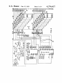
Page registers 32 consists of a 4X4 register ?le, such
More speci?cally, the S1 signal is a data bus status signal
as the SN74LS670 module manufactured and sold by
and when it is in a logic “0” state, it indicates that either
Texas Instruments, Inc. of Dallas, Tex., and described
a halt or write function is occurring and when it is in a
logic “l" state, it indicates that a read or fetch function 25 in the aforementioned book, “The TTL Data Book for
over data bus 18 and the eight data bits are labeled
is occurring. Similarly the IO/M signal indicates
Design Engineers”. Brie?y, page registers 32 consists of
whether the read/write function is directed to memory
or to an Input/Output (I/O) device. When IO/M signal
is logic “1”, the information on the data bus is desig
nated for an I/O device and when the IO/M signal is 30
a sixteen bit register ?le organized as four words of four
bits each and further consists of on chip decoding pro
viding for the addressing the four word locations in
either a write in or read out mode. This permits simulta
neous writing into one location and reading from an
logic “0”, the information on the data bus is designated
other location, if desired. The four low order data bus
for the memory. It should be noted that the IO/M signal
18 bits D0 through D3 are applied to the data input of
is in the high impedance state during the hold or halt
page registers 32. In addition, six control signals are
instructions.
The ALE signal is an address latch enable signal 35 applied to inputs, respectively labeled WB, WA, RB,
Ra, GW and GR. The signals applied to the WA and
which occurs during the ?rst clock cycle of a machine
state and enables the address to be latched. As used for
WB inputs control which one of the four words will
the present invention, the ALE signal is for the purpose
have new data written therein as long as an active logic
“0” signal is applied to the .GW input. The signals ap
all valid. In addition, the microprocessor position of 40 plied to the RA and RB inputs control which one of the
of specifying when the sixteen bits on address bus 16 are
(£1 14 provides conventional read (RD), and write
(WR) control signals. Input output device addressing
circuitry can be included within CPU 14 to respond to
four words will be read whenever an active logic “0“
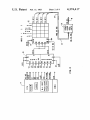
signal is applied to the GTI input. As seen in FIG. 2, the
GR input is placed at a logic “0" state by grounding and
thus at any given time, one word consisting of four bits
the RD and WR signals to provide the RD PG REG
and WT PG REG signals. The output from the DMA 45 will always be read and applied as the PG BIT 0
through 4 signals on page bit bus 34.
portion of CPU 14 is the AEN signal which signifies
In operation, if logic “0“ signals are applied to both
that a DMA transfer is occurring. Normally this signal
the WA and W8 inputs and the GW input is at logic
is logic “0", but becomes a logic “1” during a DMA
“0”, then word 0 contained within the 4X4 ?le of page
operation and is used to disable the system data and
50 registers 32 will have the data applied over lines D0
control buses during the DMA operation.
through D3 of data bus 18 written therein. As shown
Page register decode 36 is a conventional dual four
schematically, in FIG. 2, word zero is in the left-most
to-one decoder such as the SN74LS153 circuit module
word and, as will be explained hereafter, is designated
manufactured and sold by Texas Instruments, Inc. of
as the DMA page register. Similarly, if WA is logic “1"
Dallas, Tex., and which is described in the book enti
tled, “The TTL Data Book for Design Engineers”, 55 and WA is logic “0”, then word 1 will have data written
therein; if WA is logic “0” and W3 is logic “1", word 2
published by Texas Instruments, Inc. in 1978. Speci?
will have data written therein; and if both WA and WE
cally, each of the two four-to-one decode circuits have
are logic “1”, word 3 will have the data written therein.
four signals applied to the C0 through C3 inputs and
Again, as will be explained in more detail hereafter,
provide one of those four signals at the Y output
thereof, so long as the strobe signal of G input has a 60 word 1 is designated as the Write RAM page register.
Word 2 is designated as the Read RAM page register,
logic “0" signal applied thereto. The particular one of
and Word 3 is designated as the ROM page register. In
the input signals applied to the output depends upon the
writing, it should be noted that it is always necessary to
state of the signals applied to the select, or A and B,
apply a logic “0” signal to the GW output or the signals
inputs. Speci?cally, if the two signals applied to the A
and B inputs are both logic "0”, ,the C0 input signal is 65 applied to the WA and WB inputs will be ignored. Since
applied as the Y output signal. If the signals applied to
the A and B inputs are respectively logic “1” and logic
“0", then the Cl input signal becomes the Y output
the GR input is connected to ground, or logic “0", the
signals applied to the RA and RB inputs will cause one
of the four 4 bit words contained in the 4X4 ?le of page