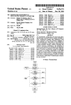
1
United States Patent [19]
[11]
4,374,417
Bradley et a].
[45]
Feb. 15, 1983
[54] METHOD FOR USING PAGE ADDRESSING
MECHANISM
[75] Inventors: David J. Bradley, Boca Raton;
Dennis D. Gibbs, Lighthouse Point;
Donald J. Kostucli, Boca Raton;
James S. Martin, Coral Springs, all of
Fla.
[73] Assignee:
International Business Machines
Corp., Armonk, N.Y.
[21] Appl. No.: 231,639
Feb. 5, 1981
[221 Filed:
.....
Int. cm
[52]
us. Cl. .................................................. .. 364/200
[56]
ABSTRACT
In a computer system, paging operates and a method of
use thereof are provided for extending the addressing
capability of a processor by using a page register. The
page register includes means for storing different codes
for different operations to be performed on the mem
ory. The memory is divided into four groups of memory
within 2" addresses such that there is paged and un
paged ROM and paged and unpaged RAM. The un
paged ROM and RAM include only a single block
which is directly addressed by the n bit address bus. The
paged ROM and RAM includes a plurality of blocks or
pages, one of which is selected to be addressed by the
[51]
. . . . . . . . . . . . . . ..
[58] Field of Search
[57]
G06F 9/30
364/200 MS File, 900 MS File
page register. The page register responds to the address
bus and to signals from the processor de?ning the mem
ory operation to be performed by providing page sig
nals, selecting one page of paged memory. The method
of using the paging apparatus includes creating a table
References Cited
U.S. PATENT DOCUMENTS
Primary Examiner—Mark E. Nusbaum
in the unpaged RAM of all routines in the paged mem
ory blocks and using the table to transfer from one
routine to another. Within the table is a code identifying
the page in which the new routine exists and an offset
into that page used to determine the address in that page
Assistant Examiner-Thomas M. Heckler
of the new routine.
3,970,999 7/1976 Elward
3,976,978 8/1976 Patterson et a1.
4,145,738
3/1979
364/200
364/200
lnoue et al. ....................... .. 364/200
Attorney, Agent. or Firm-Harry W. Barron; John C.
Black; J. Jancin, Jr.
14 Claims, 10 Drawing Figures
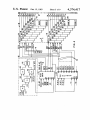
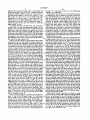
ROM
DECODE
24
,
_.._
ROM ROM
BASE
RAM
20
-
:
PAGEN
ROM
iii
PNSEN
RAM
RAM
RAM
50 JL‘
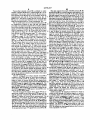
U.S. Patent
Feb. 15, 1983
lair
an
amwiz
#8m
;l
Sheet 3 of9
4,374,417
I XXX
U.S. Patent
Feb. 15, 1983
Sheet 4 of9
I a
33-7-1
4,374,417
I X
an.’
warn:
mm
m.0; 4m.0; mm.0;
U.S. Patent
Feb. 15, 1983
Sheet 5 of9
ctm3
4,374,417
‘In
:5g
US. Patent
Feb. 15, 1983
Sheet 6 of9
4,374,417
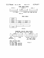
PAGE TABLE ENTRY
BYTE O
BYTE 2
BYTE
‘I
7
0
7
5'4
0
'r
0
I
I
I
1
I
L
J
TVT INDEX
OFFSET INTO PAGE SECTION
FIG. 5
PAGE TABLE
X000
XOOI
X002
X005
X003
X006
X004
X007
FIG.6
TRANSFER VECTOR TABLE ENTRY
AT LOC 8AOO+ (2%)‘ TVT INDEX)
BYTEI
O
7
BYTE 2
7
I
l
I
1
|
|
I
0 |
l
I
I
I
I
I
|
|
I
l
l
l
I
l
|
I
I
l
I
I
I
I
I
I
H_1;_Y______/
PATCH
INDICATOR
PAGE
0
l
SECTION
PAGE
\
|
v
OFFSET TO BYTE 2
OF PAGE TABLE
FOR THIS ENTRY
CODE =
OO-NOT USED
01-2000 PAGE SECTION
10-4000 PAGE SECTION
10-6000 PAGE SECTION
F|G_ 7
U.S. Patent
Feb. 15, 1983
Sheet 7 of 9
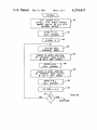
@
TVT ADD'R —- H.L
0->ALL TVT FIRST BYTES
TRAPP ADD'R TO ALL TVT
SECOND BYTES
4,374,417
/ I50
/I52
2002 —> H,L
CALL PGSCAN
I
CLEAR
A
/154
i
/156
A-> PG REG
(CURRENT PAGE)
I
CHECK IF 4000 SECTION
OF CURRENT PAGE EXISTS
8 DO A CRC CHECK
I
4002 -> H,L
was
,(160
CALL PGSCAN
CHECK IF 6000 SECTION
OF CURRENT PAGE EXISTS
8 DO A CRC CHECK
fIZ6
6002 -> H, L
CALL PGSCAN
PG REG+ I->A
FIG.8
N0
CONTINUE
U.S. Patent
4,374,417
Sheet 8 of 9
Feb. 15, 1983
Q PGSCAN :
H->D (PAGE SECTION CODE)
FIG. 9
168
/
L ->E (OFFSET T0 CURRENT
TABLE ENTRY)
RETURN IF cuRRENT PAGE
TABLE ENTRY ="FF"
OTHERWISE STORE TVT
INDEX **2 (FROM CURRENT
ENTRY IN PAGE TABLE) IN
H.L.
ADD BASE ADDRESS OF
TVT (BAOO) T0 H,L
PG REG CODE -> BITS O-3
OF B
PAGE SECTION CODE ->
BITS
/174
435 OF B
B-lv MEMORY
(TVT BYTE I)
AT H,L
E-> MEMORY AT H,L
(TVT BYTE 2)
{we
U.S. Patent
Feb. 15, 1983
Sheet 9 of9
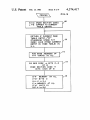
RST 1
4,374,417
ggIfLilNG SEQUENCE
NAME (2 BYTES)
ADJUST RETURN ADD'R
PAST NAME a sAvE
I
NAME->H,L
I
M“
W182
CLEAR A
sAvE OLD ROM
/./I84
PAGE VALUE
I
FIRST TVT BYTE AT H,L ->A
SET PAGE REG FOR NEW PAGE /‘/I86
H,L +‘I -> H, L
SECOND TVT BYTE AT H,L ->L
I
LEFT SHIFT A THRU C
I
/138
POSITION
//
I92
PATCH AREA
ADD'R->H,L
BITS 5,6,7 OF A->H
(PAGE SECTION
/194
BITS)
BYTE I OF PAGE TBL—>L
/196
BITS 0-4 OF BYTE 2 OF
PAGE TB|.->H
I
H,L —>Pc
W198
l
CONTINUE AT NEW
ADDRESS
/200
FIG. IO
1
4,374,417
METHOD FOR USING PAGE ADDRESSING
MECHANISM
2
program instructions storage means for storing the pro
gram instructions and means for fetching the designated
program instructions. The program instructions are
grouped together in program modules and the program
This invention relates to memory addressing and,
more particularly, to apparatus and the method for
accessing an amount of memory greater than can be
normally accessed using a given size address bus.
instruction storage means is divided into a plurality of
' pages. Each page includes at least one page section and
at least one program module having an identi?cation
code associated herewith resides in each page section.
It is well known from the prior art that one can in
Each page is selectable so that one program instruction
crease the size of memory addressed by an address bus 10 in that page is directly addressed by the program
carrying N bits of information from the normal 2Nloca
tions to some multiple of 2” by utilizing the technique of
paging. This technique generally is implemented by
providing a large memory having pages broken into 2”
addressable segments and further providing an external
register which can be set by a processing unit to provide
a given code selecting one of the various pages. An
example of such a system is shown in U.S. Pat. No.
4,037,211 to Ikuta et a1, granted July 19, 1977.
In utilizing a paged memory scheme to its fullest
advantage, some easy and simpli?ed procedure must be
established to allow for the orderly and automatic trans
counter, whereby the addressed instruction is desig
nated. The improvement is a method of fetching pro
gram instructions from a different program module
comprising the steps of tabulating in a page table for
each paged section, each program module identi?cation
code in that section and the address in that section for
that module and scanning each page section table to
create a transfer vector table in the random access mem
ory. The transfer vector table is addressed in accor
dance with the identi?cation code of each program
module and includes a pointer to the page section in
which the program module having the identi?cation
code resides. The method further comprises the steps of
looking up the pointer for the identi?cation code of the
loop will exist which, in response to various external 25 different program module in the transfer vector table,
events such as the depression of a key on a keyboard or
processing the looked up pointer to obtain the address
fer of addressing from one page to another. For in
stance, in a typical program, a basic system operating
the request for more information to be printed by a
of the different program module and to select the page
in which the new program module resides and storing
the
obtained address in the program counterr
one departure will be contained as a separate program 30
In utilizing this method, a programmer now need
module which physically exist in a different page than
only assign an arbitrary identi?cation code to each pro
printer, will cause departures from the basic loop. Typi
cally the program governing the result desired for any
the basic loop. In preparing the program, programmers
gram module and then provide the appropriate transfer,
typically prepare each group of instructions constitut
by
way of, for instance, call or jump instructions, to the
ing a program module separate and apart from one
another. Not until the programming has been com 35 coded identi?cation number. Other program modules
within the total program can then utilize the tables
pleted is each of the program modules stored in mem
provided (which identify the location of the program
ory. The precise organization of the memory and the
module) to cause a transfer to that module. This greatly
modules will depend on the size of each individual mod
simpli?es the programmer’s task in preparing the pro
ule. For example, for large program modules, it may be
gram and provides an automatic mechanism to allow
possible to store only a relatively few in a page of mem
the
transfer from one program module to another be
ory. On the other hand, for short modules, a large num
fore all of the individual program module are known or
ber can be stored on each page. In practice, both large
their speci?c addresses in the program storage means
and some small modules are assigned to each page so
are determined.
that the maximum possible locations per page are uti
One preferred embodiment of this invention is herein
45
lized.
after described with reference being made to the follow
During the initial programming, the programmer is
unable to determine precisely which page a program
module will be assigned and hence the programmer
cannot program in the necessary page enabling codes
needed to transfer program control from one module to
another. Accordingly, some scheme must be developed
to allow this to be easily and automatically accom
plished, irrespective of where the program modules are
ultimately placed. During the programming process, all
that can be required of the programmer is to cause a 55
transfer from one identi?ed (by name or identi?cation
ing drawings in which:
FIG. 1 is a block diagram showing the addressing
apparatus for addressing a page memory;
FIG. 2 shows in more detail the central processor
unit and the paged bit generating means of the address
ing circuit shown in FIG. 1;
FIG. 3 shows in more detail the read only memory
and the address decoding circuit therefore, shown in
FIG. 1;
FIG. 4 shows in more detail the random access mem
ory and controller and decoding circuit therefore
number) program module to another identi?ed program
shown in FIG. 1;
module without considering the location of either. One
FIG. 5 shows a page table entry;
way to do this is to utilize a table storing the program
FIG. 6 shows the organization of the page table
names by identi?cation number together with an associ 60
within one page section;
ated page number and address within the page in a
FIG. 7 shows a transfer vector table entry;
master table for the identi?ed program.
FIG. 8 shows a ?ow diagram representing a series of
In accordance with one aspect of this invention, there
program instructions used for building the transfer vec
is provided an improvement in a data processing system
which executes a series of fetched program instructions 65 tor table;
FIG. 9 shows a ?ow diagram representing a series of
to obtain a desired result and which includes a program
program instructions used in scanning the page table in
counter for providing an address code, random access
each page section of program storage memory; and
memory directly addressable by the program counter,
3
4,374,417
FIG. 10 shows a flow diagram for a sequence of
program instructions allowing for the transfer from one
program module to another.
Referring now to FIG. 1, paging apparatus 10 is
shown and is used for addressing a paged memory 12 in
4
the embodiment described herein in FIGS. 2-4, M is
selected to be three.
Page registers 32 may consist of a plurality of regis
ters, each of which is assigned to a different function to
be performed by CPU 14. For instance, if an operation
fetch function is performed by CPU 14, whereby a
unit (CPU) 14. CPU 14 may consist of an Intel 8085
program instruction is read from paged ROM 24, one of
microprocessor manufactured and sold by Intel Corp.
the registers in page registers 32 will be enabled to
of Santa Clara, Calif, together with other circuits nor
provide the page bits on bus 34. Separate registers
mally associated with an 8085 microprocessor such as 0 within page registers 32 are also provided for the opera
an 8257 direct memory access (DMA) controller. CPU
tions of reading from the paged RAM 30, writing into
14 provides signals over an address bus 16, a data bus 18
the paged RAM 30 and DMA operations in which the
response to signals provided from a central processing
and a control bus 20. The address bus 16 contains six
teen lines, whereby CPU 14 can directly address 65,536
(64K) locations of memory. As described herein, each
location will be considered to be the equivalent of eight
binary digits (bits) or, one byte, of information. Data bus
18 consists of eight lines used for carrying eight bits, or
DMA is utilized to read or write from paged RAM 30.
Of course, page registers 32 may include additional
registers for other functions desired to be performed by
CPU 14.
Page registers 32 respond to signals provided thereto
from data bus 18 and to a write page register signal (WT
one byte, of information between CPU 14 and memory
PG REG) provided by CPU 14. In addition, register
12, as well as between CPU 14 and other portions of 20 selection signals are provided to select one of the plural
addressing apparatus 10 requiring data to be provided
ity of registers within page registers 32 from page regis
ter decode circuit 36. The selection signals from page
register decode 36 will select one of the registers within
signify different operations which are to be performed
page registers 32 to provide data on to page bits bus 34.
by CPU 14. For instance, if memory 12 is to be read, 25 If the WT PG REG signal from CPU 14 is active, the
one set of signals will appear on control bus 20, whereas
data appearing on data bus 18 will be written into the
if the information on data bus 18 is to be written into
selected register in page registers 32.
memory 12, a different set of signals will appear on
CPU 14 can also read the signals provided by page
control bus 20. The detailed description of the various
registers 32 by the provision of the read page register
signals appearing on control bus 20 will be described
signal (RD PG REG) to enable the read page register
hereafter when a more speci?c description of CPU 14 is
gate 38. Read page register gate 38 responds to the page
given in FIG. 2.
bit signals on page bit bus 34 and provides these signals
back to data bus 18 when the gates therein are enabled
Memory 12 consists of read only memory (ROM) and
by the RD PG REG signal from CPU 14.
random access memory RAM), each addressable within
The selection of either the base ROM 22 or one page
the 64K addressing space of address bus 16. The first 35
of the paged ROM 24 is controlled by the ROM address
32K address space is used for read only memory in
decode circuit 26. ROM address decode 26 responds to
which the various program modules are stored. The
signals on address bus 16 and the page bits on page bit
read only memory is further broken down into un
bus 34 to provide one active chip select signals on chip
paged, or base, ROM 22 contained within the ?rst 16K
address locations and paged ROM 24 contained within 40 select bus 40 to enable at least a portion of one of either
the base ROM 22 or one page of paged ROM 24 to
the address locations between 16K and 32K. The paged
respond to the address signals on address bus 16. The
ROM 24 is divided into zero through N pages of 16K
exact operation of this will be explained in more detail
bytes each. At any given time only one of the zero
with respect to FIG. 3.
through N pages will be enabled by chip select signals
The selection between base RAM 28 and paged
applied thereto from ROM address decode circuit 26. 45
RAM 30 is controlled by RAM controller 42 and col
The random access memory is organized similar to
umn address strobe (CAS) decode 44. RAM controller
the read only memory in that unpaged base RAM 28
42 responds to the signals on address bus 16 and control
exists from the address locations from 32K to 48K and
bus 20 and provides a CAS signal, two row address
zero through N pages of paged RAM 30 exits from
locations 48K through 64K. With regard to the paged
strobe (RAS) signals, RASI] and RASl, and seven
RAM 30, at any given time only one of the pages may
RAM address signals (RAM All-A6) over RAM ad
dress bus 46. The CAS signal and the page signals on
be selected. This selected page will respond to address
page bit bus 34 are applied to CAS decode 44 which
signals on address bus 16 from 48K through 64K. It
provides the CASO through N signals over CAS bus 48.
should be noted that any address signal between 32K
The CAS, RASl], RAS] and the RAM address bus 46
and 48K will automatically address base RAM 28.
signals are applied to base RAM 28 and the RASl, the
The particular one of the pages selected from paged
CAS bus 48 and the RAM address bus 46 signals are
ROM 24 or paged RAM 30 is determined by the signal
applied to the paged RAM 30 to select at least a portion
at the output of page registers 32. This signal, referred
of one of the RAM pages and address one location
to as Page Bits 0 through M is provided from one of a
plurality of selected page registers within page registers 60 within that page. The details of the addressing scheme
of the RAM is described in more detail in FIG. 4.
32 over page bits bus 34. The number of page bits,
Referring now to FIG. 2. A more detailed diagram of
M+ I, provided from page register 32 will determine
hereto or which provides data to be sent to CPU 14.
Control bus 20 consists of a plurality of lines which
CPU 14, page register decode 36, page registers 32, and
the number of possible pages of each of paged ROM 24
read page register gate 38 is shown. CPU 14 consists of
and paged RAM 30. For instance, if M'is equal to seven,
whereby eight page bits are provided, then the number 65 a microprocessing unit such as an Intel 8085 micro
processor and a DMA device, such as the Intel 8257,
of pages will be 256 or, if M is equal to three, whereby
both of which are manufactured and sold by Intel Corp.
four page bits are provided, the number of the pages of
of Santa Clara, Calif.
paged ROM 24 or paged RAM 30 will be sixteen. For
5
4,374,417
The microprocessor includes an accumulator, or A,
6
signal. If the signals applied to the A and B inputs are
register and six other temporary storage registers which
respectively logic “0" and logic “l”, then the C2 input
are identi?ed as the B, C, D, E, H and L registers. These
registers can be used individually or in groups of two,
such that the B and C registers form one group, the D
and E registers form a second group, and the H and L
signal becomes the Y output signal and if both the A and
B signals are logic “1”, then the C3 input signal be
comes the Y output signal. As coupled in page register
decode circuit 36, two four-to-one decode circuits are
registers form a third group. In addition, there is a pro
gram counter, a stack pointer and conventional com
utilized, both of which are provided in the single
SN74LS153 module. The 1C0 through 1C3 inputs of
puter logic in the microprocessor. Reference is made to
the manual entitled, “MCS-85 User‘s Manual”, pub
lished by Intel Corporation in 1978 for a more complete
description of CPU 14.
The microprocessor part of CPU 14 provides a six
teen bit address signal over the address bus 16. The
address signals are respectively labeled All through
A15. In addition, an eight bit data signal is provided
the upper four-to-one decode circui_t_are respectively
coupledto a logic “1” signal, the A15 signal, the A0
signal, and the A0 signal. The lower four inputs, 2C0
through 2C3, are respectively coupled to the m sig
nal, a logic “1” signal, the Al signal and the A1 signal.
The strobe signals TG and TG for both portions are
connected to the AEN signal from the DMA portion of
CPU 14 and the A and B select signals are respectively
coupled to the S1 and IO/M signal from the micro
processor portion of CPU 14. The Y output of the upper
respectively D0 through D7. The control bus 10 from
four-to-one decode circuit is labeled the OUT A signal
CPU 14 consists of at least the S], the IO/?, and ALE
signals, all of which are well known and described in 20 and the Y output from the lower portion of the four
to-one decode circuits is labeled the OUT B signal.
detail in the aforementioned “MCS-85 User’s Manual”.
Page registers 32 consists of a 4X4 register ?le, such
More speci?cally, the S1 signal is a data bus status signal
as the SN74LS670 module manufactured and sold by
and when it is in a logic “0” state, it indicates that either
Texas Instruments, Inc. of Dallas, Tex., and described
a halt or write function is occurring and when it is in a
logic “l" state, it indicates that a read or fetch function 25 in the aforementioned book, “The TTL Data Book for
over data bus 18 and the eight data bits are labeled
is occurring. Similarly the IO/M signal indicates
Design Engineers”. Brie?y, page registers 32 consists of
whether the read/write function is directed to memory
or to an Input/Output (I/O) device. When IO/M signal
is logic “1”, the information on the data bus is desig
nated for an I/O device and when the IO/M signal is 30
a sixteen bit register ?le organized as four words of four
bits each and further consists of on chip decoding pro
viding for the addressing the four word locations in
either a write in or read out mode. This permits simulta
neous writing into one location and reading from an
logic “0”, the information on the data bus is designated
other location, if desired. The four low order data bus
for the memory. It should be noted that the IO/M signal
18 bits D0 through D3 are applied to the data input of
is in the high impedance state during the hold or halt
page registers 32. In addition, six control signals are
instructions.
The ALE signal is an address latch enable signal 35 applied to inputs, respectively labeled WB, WA, RB,
Ra, GW and GR. The signals applied to the WA and
which occurs during the ?rst clock cycle of a machine
state and enables the address to be latched. As used for
WB inputs control which one of the four words will
the present invention, the ALE signal is for the purpose
have new data written therein as long as an active logic
“0” signal is applied to the .GW input. The signals ap
all valid. In addition, the microprocessor position of 40 plied to the RA and RB inputs control which one of the
of specifying when the sixteen bits on address bus 16 are
(£1 14 provides conventional read (RD), and write
(WR) control signals. Input output device addressing
circuitry can be included within CPU 14 to respond to
four words will be read whenever an active logic “0“
signal is applied to the GTI input. As seen in FIG. 2, the
GR input is placed at a logic “0" state by grounding and
thus at any given time, one word consisting of four bits
the RD and WR signals to provide the RD PG REG
and WT PG REG signals. The output from the DMA 45 will always be read and applied as the PG BIT 0
through 4 signals on page bit bus 34.
portion of CPU 14 is the AEN signal which signifies
In operation, if logic “0“ signals are applied to both
that a DMA transfer is occurring. Normally this signal
the WA and W8 inputs and the GW input is at logic
is logic “0", but becomes a logic “1” during a DMA
“0”, then word 0 contained within the 4X4 ?le of page
operation and is used to disable the system data and
50 registers 32 will have the data applied over lines D0
control buses during the DMA operation.
through D3 of data bus 18 written therein. As shown
Page register decode 36 is a conventional dual four
schematically, in FIG. 2, word zero is in the left-most
to-one decoder such as the SN74LS153 circuit module
word and, as will be explained hereafter, is designated
manufactured and sold by Texas Instruments, Inc. of
as the DMA page register. Similarly, if WA is logic “1"
Dallas, Tex., and which is described in the book enti
tled, “The TTL Data Book for Design Engineers”, 55 and WA is logic “0”, then word 1 will have data written
therein; if WA is logic “0” and W3 is logic “1", word 2
published by Texas Instruments, Inc. in 1978. Speci?
will have data written therein; and if both WA and WE
cally, each of the two four-to-one decode circuits have
are logic “1”, word 3 will have the data written therein.
four signals applied to the C0 through C3 inputs and
Again, as will be explained in more detail hereafter,
provide one of those four signals at the Y output
thereof, so long as the strobe signal of G input has a 60 word 1 is designated as the Write RAM page register.
Word 2 is designated as the Read RAM page register,
logic “0" signal applied thereto. The particular one of
and Word 3 is designated as the ROM page register. In
the input signals applied to the output depends upon the
writing, it should be noted that it is always necessary to
state of the signals applied to the select, or A and B,
apply a logic “0” signal to the GW output or the signals
inputs. Speci?cally, if the two signals applied to the A
and B inputs are both logic "0”, ,the C0 input signal is 65 applied to the WA and WB inputs will be ignored. Since
applied as the Y output signal. If the signals applied to
the A and B inputs are respectively logic “1” and logic
“0", then the Cl input signal becomes the Y output
the GR input is connected to ground, or logic “0", the
signals applied to the RA and RB inputs will cause one
of the four 4 bit words contained in the 4X4 ?le of page
7
4,374,417
registers 32 to always be read. Thus, a 4 bit signal will
always be applied as the PG BIT 0-3 signals on bus 34.
Again, if both RA and RB are logic “0”, then word 0 or
the DMA page register, is read. If RA is logic “1" and
RB is logic “0”, then word 1 or the Write RAM page
register is read. If RA is logic “0" and RB is logic “1”,
then word 2, or the Read RAM page register, is read.
be logic “1" and, hence, word 3, or the ROM page
register, will be selected.
Connected in this manner, it is seen that the sequence
of instructions, such as reading a program instruction
from the ROM followed by a reading of data from one
page of the RAM and writing of data into a different
page of the RAM, can automatically occur without the
And ?nally, if both RA and RB inputs have logic “1"
necessity of setting a page register between each in
signals supplied thereto, then the word 3, or the ROM
struction. In other words, the ROM page register, the
10 Read RAM page register and the Write RAM page
page register, is read.
Four page bits from the particular one of the four
words of the 4X4 file containing page registers 32 are
applied as the PG BIT 0-3 signals on page bits bus 34.
Each line of bus 34 is applied as one input to one of four
gates within read page register gate 38. The other input
of each gate has applied thereto the RD PG REG signal
register are all initially set and then the sequence of
instructions just described is expected and automati
cally causes the appropriate page bits to be provided for
the desired function. In this same manner, if a DMA
operation is included, a separate set of page bits can be
provided in the DMA page register, thereby eliminating
from CPU 14 to enable the gates to provide the PG BIT
the requirement of resetting that page register each time
a DMA operation occurs.
0-3 signals to the data bus 18. Thus, read page register
gate 38 allows CPU 14 to read the page signal informa
Whenever it is desired to write new information into
20
tion read from page registers 34.
the page registers 32 or for CPU 14 to read the informa
The RA and WA inputs to page registers 32 are both
tion stored by page registers 32, page registers 32 are
connected to the OUTA signal from page register de
treated as an input output, or I/O device. In this case,
code 36. The RB and WB inputs to page registers 32 are
the IO/M signal becomes logic “1" and the S1 signal
both connected to the OUTB output from page register
will be logic "0” or logic “1”, depending upon whether
to code 36. Connected in this manner, the signals at the
information is being written into or read from page
outputs of page register decode 36 control the particu
registers 32. In either case, the OUTA signal becomes
lar word which is read from the page registers 32 and
the A0 address signal and the OUTB signal becomes the
applied to page bit bus 34 as the PG BIT 0-3 signals.
A1 address signal. By appropriately addressing page
The OUTA and OUTB signals from page register de 30 registers 32 with the A0 and A1 address signals, either
code 36 will each be one of the signals applied to the C0,
of the four words can be read or written over, in con
C1, C2 or C3 inputs of the two parts of page register
junction with the provision of the WT PG REG signal
decode 36, depending on the state of the S1 and IO/M
or the RD PG REG signal from CPU 14. Referring
bar signals applied to the A and B inputs of the AEN
now to FIG. 3, a more detailed diagram of the ROM
address to decode circuit 26 is shown in conjunction
signal applied to the 1G and 26 inputs. In the case of a
with the base ROM 22 and the paged ROM 24 of the
DMA operation, the AEN signal becomes logic "1”,
thereby causing the OUTA and OUTB signals to both
memory 12. ROM address decode 26 includes a pair of
two-to-four decode circuits 50 and 52 and a pair of
become logic “0”. These signals, when applied to the
three-to-eight decode logic circuits 54 and 56. As
RA and RB inputs of page registers 32, cause the DMA
page register, or word 0, to be read and the bits stored
shown in FIG. 3, only pages, 0, 1, 4, 5, 6 and 7 are
therein become the PG BIT 0-3 signals applied to page
shown for paged ROM 24, it being understood that any
bit bus 34. In the event it is desired to write information
number of pages up to sixteen can be used. As previ
ously explained with respect to FIG. 1, the unpaged
into the random access memory, the S1 signal becomes
ROM 22 includes 16K bytes in address space 0-16K and
logic “0" and the IO/M signal is logic “0". In this event,
the CO inputs to both portions of the four-to-one de 45 each page of the paged ROM 24 of the ROM memory
includes 16K bytes in address space l6K-32K. How
code circuits making up page register decode 36 be
ever, in actually constructing the system, two circuit
come the OUTA and OUTB signals. In other words,
modules of 8K bytes may be used for the unpaged ROM
the OUTA signal becomes logic “1" and the OUTB
signal becomes the value of signal Til-5 which is the
22 and for each page of the paged ROM 24. Thus, the
complement of the signal on address line 15. In the case 50 unpaged ROM 22 includes ?rst section 58 and second
section 60, each of which are 8K bytes in size. Similarly,
of the rarldgm access memory, the organization is such
page 0 of the paged ROM 24 includes section 62 and
that the A15 signal will be logic “0” when this part of
section 64. The same is true for each of the other pages
the memory is accessed. Thus, the OUTB signal will be
wherein page 1 includes sections 66 and 68, page 4
logic "0" for a write to RAM memory operation. This,
in turn, makes the RA signal logic “1” and the RB signal 55 includes sections 70 and 72, page 5 includes sections 74
and 76, page 6 includes sections 78 and 80 and page 7
logic “0” and, hence, word 1 or the Write to RAM page
includes sections 82 and 84.
register is selected to be read and provide the PG BIT
Two-to-four decode circuit 52 is utilized to select
0-3 to the page bits bus 34.
which of the two sections 58 or 60 of the unpaged ROM
For a read from memory operation, the S1 signal is
logic “1” and the 10/“ signal is logic “0”. In this case, 60 22 is to be addressed by the A0 through A12 address
signals. Three-to-eight decode circuit 54 is utilized to
the C1 input to the two parts of the dual four-to-one
select which one of the four sections 62, 64, 66 and 68 of
decode circuit within page register deeode__3_6 is se
pages 0 and 1 are to be addressed by the address signals
lected and the OUTA signal becomes the A15 signal
A0 through A12 on address bus 16. Three-to-eight de
and the OUTB signal becomes a logic “1". If the read is
from the random access memory, I? is logic “0” and, 65 code circuit 56 is utilized to determine which one of the
sections 70, 72, 74, 76, 78, 80, 82 and 84 of pages 4, 5, 6
hence, word 2, or the read from RAM, of page registers
or 7 are to be addressed by the address signals A0
32 will be selected. On the other hand, if the read is
through A12 on address bus 16.
from the ROM part of the memory, the msignal will
9
4,374,417
10
The data outputs from each of ROM sections 58, 60,
62, 64, 66 and 68 are coupled together and applied to the
Two-to-four decode circuit 50 is utilized to select
whether unpaged ROM 22 or paged ROM 24 is to be
addressed. Two-to-four decode circuit 50 and two-to
four decode circuit 52 may be circuit modules 741.5139
data input of bus driver circuit 86. In the same manner,
two-to-four decode circuit 50 is connected to the ALE
decoders 90 and 92 may be conventional 74LSl39 cir
cuits and OR gate 94 may be a 74LS08 circuit having
the data outputs from each of the modules 72, 74, 76, 78,
80, 82 and 84 are coupled together and applied to the
manufactured and sold by Texas Instruments, Inc. of
data input of bus driver 88. Bus driver circuits 86 and 88
Dallas, Text, and three-to-eight decode circuits 54 and
may be conventional 74LS244 driver circuits manufac
56 may be conventional 74LS138 circuit modules also
tured and sold by Texas Instruments, Inc. of Dallas,
sold and manufactured by Texas Instruments, Inc.
Tex. At any given time, only one of these circuits, 86 or
The A and B inputs to two-to-four decode circuit 50
are respectively coupled to the A14 and A15 signals 0 88, may be enabled by the operation of a pair of two-to
four decoders 90 and 92 and OR gate 94. Two-to-four
provided over address bus 16. TheG', or enable, input to
signal provided from CPU 14 at the beginning of each
cycle of operation of CPU 14. When both the A14 and
A15 signals are logic “0", the Y0 output from two-to
four decode circuit 50 becomes logic “0”; otherwise, it
is logic "1”. When the A14 signal is logic “1” and the
A15 signal is logic “0", the Y1 output from two-to-four
decode circuit 50 becomes logic “0”; otherwise, it is
logic “I". The Y2 and Y3 outputs from two-to-four
inverted logic inputs and an inverted logic output. The
A and B inputs to decode circuit 90 are respectively
coupled to the A14 and A15 signals and the enable, orG
input to circuit 90 is coupled to the MEMR signal,
which may be generated by means (not shown) respon
sive to both the RD and IO/M signals from CPU 14
20 whenever it is desired to read information from the
memory. The Y0 output from decode circuit 90 is cou
decode circuit 50 are unconnected, as shown in FIG. 3.
pled as one input to OR gate 94 and the Y1 output from
The Y0 output from two-to-four decode circuit 50 is
decode circuit 90 is coupled to the enable, or G, input of
coupled to the G, or enable, input of two-to-four de
two-to-four decode circuit 92. The A and B inputs to
code circuit 52. Whenever the Y0 signal from two-to 25 decode circuit 92 are respectively coupled to the PG
four decode circuit 50 is logic “0”, two-to-four decode
BIT2 and PG BIT3 signals from page registers 32. The
circuit 52 is enabled. The A and B inputs of two-to-four
Y0 output from decode circuit 92 is coupled as the
decode circuit 52 are respectively coupled to the A13
second input to OR gate 94 and the Y1 output from
address signal and to a logic “1” signal. When two-to
decode circuit 92 is coupled to the chip select (C8)
four decode circuit 52 is enabled and if the A13 signal
input of bus driver 88. The output of OR gate 94 is
applied to the A input is a logic “0”. then the Y2 output
coupled to the chip select (ti-S’) input of bus driver 86.
from two-to-four decode circuit 52 becomes logic “0”.
Connected in this manner whenever information is read
If the A13 signal is a logic “I”, the Y3 output from
from one of thw ROM sections 58, 60, 62, 64, 66 or 68,
two-to-four decode circuit 52 becomes a logic “0”. The
bus drive 86 is enabled and whenever information is
Y2 signal from circuit 52 is provided to the chip select
read from one of the ROM sections 70,72, 74, 76, 78, 80,
input of section 58 of unpaged ROM 22 and the Y3
82 or 84, bus driver 88 is enabled. The output of each of
output from circuit 52 is applied to the chip select input
bus drivers 86 and 88 is connected to the data bus 18,
of section 60 of unpaged ROM 22. Whenever a logic
which carries the D0 through D7 data signals.
"0” signal is applied to the chip select input of one of the
Referring now to FIG. 4, RAM controller 42, CAS
ROM sections 58, 60, that particular section is enabled
decode 44, unpaged RAM 28 and the paged RAM 30
to respond to the address signals A0 through A12 on
are shown in more detail. RAM controller 42 may be a
address bus 16. In response to these addresss signals and
conventional RAM memory controller, such as the
the chip select enabling signal, eight bits of data con
Intel 8202 random access memory controller, manufac
tained in the address location are provided at the output
tured and sold by Intel Corp. of Santa Clara, Calif.
of the enabled section.
45 RAM controller 42 is enabled by a logic “0" signal
The Y1 output of two-to-four decode circuit 50 is
being applied to the C8 or chip select input thereof from
coupled to the G21 inputs of both three-to-eight de
logic circuit 86. This signal, as will be explained in more
code circuits 54 and 56. In addition, the A, B, and C
detail hereafter, is provided when the A15 address sig
inputs to each of circuits 54 and 56 are respectively
nal is logic “1” and the PG BIT3 signal is logic “0” or
coupled to the A13 address signal and the PG BITO and 50 in other words, when the random access memory 28
and 30 is selected. As shown in FIG. 4, there is one
LG BITI page bit signals from page registers 32. The
G1 input to circuit 54 is coupled to the PG BIT2 signal
unpaged block of 16K RAM and seven paged blocks of
16K RAM. Thus, only three PG BITSO-2 of the four
and them input to circuit 54 is connected to the PG
BIT3 signal. The GT inpujgcircuit 56 is coupled to the
paged register 32 signals PG BITO-3 are required.
PG BIT3 signal and the G23 input to circuit 56 is cou 55 Hence, under normal operations, the PG BIT3 signal is
always kept at logic “0”.
pled to the PG BIT2 signal.
The Y0 through Y3 outputs from circuit 54 are re
spectively coupled to the chip select (CS) inputs of the
RAM controller 42 includes an address bus input to
which the A0 through A13 address signals are applied.
In addition, there is a clock input to which the sysEm
page 0 and page 1 sections 62, 64, 66 and 68. The Y4
through 7 outputs of circuit 54 are unconnected. The 60 clock of 16.432 me ahertz is applied, a write (WT)
in ut to which the MEMW si al is applied, a read
Y0 through Y7 outputs of circuit 56 are respectively
coupled to the chip select (C§) inputs of page 4, page 5,
page 6 and page 7 sections 70, 72, 74, 76, 78, 80, 82 and
( ) input to which the MEMR signal is applied, a B0
input to whi£l_1_the A14 address signal is applied, and the
chip select (CS) in at to which the output of logic 86 is
84. Each of the paged ROM sections respond to address
bits A0 through A12 applied thereto over address bus 65 applied. The MEMW signal is provide§l__by logic (not
shown) responsive to the WR and lO/M signals from
16 and provides an 8 bit output signal containing the
CPU 14, whenever these signals indicate that a memory
addressed data when that particular module is selected
write operation is to occur.
by an appropriate logic “0” signal from circuit 54 or 56.
11
4,374,417
12
puts include a RA§0, RASl, IVE (Write Enable) and
ms signals. The RASO and RASl signals are provided
CAS decode 44 is applied to pages 1-7 respectively.
Thus, it is seen that the RASO and mi signals are
used to determine whether base RAM 28 or paged
RAM 30 is to be accessed and the CE and W1
through CAS7 signals are used to determine which
as row address strobes and the particular one provided
page is to be accessed.
is determined by the value of the A14 signal applied to
the B0 input. If A14 is logic “0" then, the RASO signal
is active. If A14 is logic "1”, the RASI signal is active.
The CAS signal is a column address strobe signal and is
Circuit 86, as previously mentioned, provides the
chip select signal to RAM controller 42. Circuit 86
consists of NAND gate 134, AND gates 136, 138 and
140, and NOR gates 142. The two inputs to NAND gate
134 are the AEN signal from the DMA portion of CPU
14 and the IO/M signal from CPU 14. The output of
The outputs of RAM controller 42 include the RAM
address bus 46 having the RAM A0 through RAM A6
address signals provided thereon. In addition, the out
applied to CAS decode circuit 44 which may be a three
to-eight decoder, such as the 74LS138 circuit manufac
tured and sold by Texas Instruments, Inc.
The A, B and C inputs of three-to-eight decoder 44
are respectively coupled to the PG BITO, PG BIT] and
NAND gate 134 is applied as one input to AND gate
136, the other input of which is the ATS- address signal.
The output of AND gate 136 is applied to one input of
PG BIT2 signals provided from page register 32. The
each of AND gates 138_a_nd 140. The other input to
AND gate 138 is the A14 signal and the other two
G1 input of three-to-eight decode circuit 44 is a logic
inputs to AND gate 140 are respectively the A14 ad
"1” signal and the G28 signal is a logic “0”. The CAS
dress signal and the PG BIT3 signal. The output of each
signal from RAM controller 42 is applied to the m
input. The seven least signi?cant outputs Y0-Y6 of 20 of AND gates 138 and 140 are applied as the two inputs
to NOR gate 142, which provides the signal to the chip
three-to-eight decode circuit 44 are utilized and respec
select input of RAM controller 42. Coupled in this
tively provide the CAS] through Cm signals on CAS
manner, the output of NOR gate 142 will be logic “0”
bus 48.
whenever the A15 address signal is logic “1" and the
The organization of the RAM 28 and 30 is somewhat
different in details than the organization of the ROM 22 25 PG BIT3 signal is logic “0".
Referring now to FIGS. 5 through 10, one technique
and 24 shown in FIG. 3. Each memory module desig
for utilizing the paging structure shown in FIGS. 1
nated 96 through 130 (even numbers only) of the RAM
through 4 will now be described. Speci?cally, FIGS. 5
28 and 30 is a 32K by I bit module and consists of two
and 6 show diagrams useful in understanding the page
16K by I bit circuits. Each circuit is respon? to the
RAM A0 through A6 address signals, the WE signal 30 table, which is present in each section of paged ROM 24
as well as in section 2 of unpaged ROM 22. FIG. 7
and to a CKSX and RASX signal. In each block (paged
shows a diagram useful in understanding the organiza
or unpaged) of RAM memory, there is one circuit from
tion of the transfer vector table, which is built from the
each of nine individual modules, such as 96-112 (even
numbers only), for providing the D0 through D7 signals
plus an additional parity bit signal labeled DP. The
parity bit DP is used by circuitry (not shown) in a con
information stored in the page tables of each section of
35 ROM 22 and 24 and which is present in a part of the
unpaged portion of RAM 28.
ventional manner to determine the parity of the data
FIG. 5 shows one entry of a page table. Each page
provided to or from RAM memory 28 or 30.
In FIG. 4, 64K bytes of random access memory are
table entry consists of three bytes of information or 24
bits in total. Eleven of the 24 bits are utilized for con
shown and divided into a 16K byte unpaged base, or 40 taining a code referred to as the TVT index. The TVT
index is a unique number for each program module. The
RAM 28 and seven pages of 16K bytes each of paged
remaining thirteen bits of information in the page table
RAM 30. It should be noted that pages 3-5 inclusive are
entry contain a number which is an offset into that
represented by the dashed lines in FIG. 4. Each of the
paged section de?ning the exact location of the pro
memory modules 96-130 (even numbers) is divided in
half so that one 16K circuit therein is part of either the 45 gram module identi?ed by the TVT index. The particu
lar organization is such that the high eight bits of the
base of one page and the other 16K circuit therein is
TVT index are contained in byte zero of the page table
part of a different page. As previously mentioned, each
entry and the low three bits are contained as bits 5, 6
16K block of memory respgrgs to address lines
and 7 of byte two. The high ?ve bits of the offset are
RAMAO-6, a RASX signal, the WE signal and a CASX
signal. For instance, the unpaged RAM 28 block is 50 contained in bits zero through 4 of byte two and the low
eight bits are contained in byte one, of the page table
shown in the upper half of modul_e_s_96-112 (evgpum
bers) and responds to the RASO WE and the CAS sig
entry.
nals as well as the RAM address bus 46 signals
with the RAM address signals RAMAO-6 on bus 46.
For page 6, shown as the upper half of modules 114-130
FIG. 6 shows the organization of a paged table. The
?rst two bytes in any paged section are located in ad
dresses X000 and X001, where X=2, 4 or 6 and corre
sponds to the section code. Those bytes contain the
high value of the ?rst address and the high value of last
address plus one of that page section. These values are
(even numbers only), the m, ‘WE and CA§6 signals
used in the initialization procedures for performing
RAMAO-6. The lower half of the module 96-112 (even
numbers only) contain?ge 1 of paged RAM 30 and
respond to the m1 WE and CAS] signals together
are applied to each of the nine 16K by 1 bit circuits of 60 certain checks on the memory to insure that it operates
properly. As such, they form no part of the present
modules 114-130 (even numbers). In the same manner,
invention. Beginning with hexadecimal location X002,
the RASl, WP: and CAS7 signals are applied to page 7.
the ?rst three byte page table entry occurs. The second
In each case, the RAM address signals RAMAO-6 on
page table entry then begins at location X005 and so
RAM address bus 46 are also applied to each circuit. In
general, for the unpaged base RAM 28, the RASO and 65 forth, so that there is one entry for each program mod
ule contained in that particular ROM section. In the
CKS signals are applied; and for the various pages of
location immediately following the last or Nth page
the paged portion, and RASl signal is applied to each
table entry, the data code hexadecimal “FF" is entered
page and one of the CASl through CAS7 signals from
13
4,374,417
to mark the end of the page table. In the location imme
diately following the end of table marker, the code for
the ?rst program instruction of the ?rst program mod
ule exists.
Referring now to FIG. 7, one entry in the transfer
vector table is shown. The transfer vector table is lo
cated in a block of unpaged random access memory 30
beginning, for instance, at location 8A00 and includes a
two byte entry for each page table entry in all of the
sections of paged and the one section of unpaged mem
ory. The transfer vector table entries are each placed in
a memory location corresponding to the TVT index
code, such that twice the TVT index is added to hexa.
decimal location 8A00. For each entry, bit 0 through 3
of byte 1 contain the page number and bits 4 and 5
contain the section code X for that page. For bits 4 and
5 the code “00” is not used; the code “01” indicates a
2000 page section, or the second part of the unpaged or
base ROM 22; the code of “10” indicates a 4000 address
in the page section or, in other words, the low ad
dressed half of each page; the code “11” indicates a 6000
address in the page section or the high addressed half of
each page. Bit 6 of byte 1 is always set equal to “O” and
14
the second byte is an offset into section 58 of unpaged
ROM 22.
Next according to block 152, the hexadecimal num
ber 2002 is transferred to the HL registers and the sub
program PGSCAN is called. The PGSCAN program is
shown in FIG. 9 and will be discussed in detail hereaf
ter. Brie?y the PGSCAN program scans the page table
for the module addressed by the HL registers and places
these scanned entries from one page table into the TVT
table in the unpaged RAM 28. Thereafter, according to
block 154, the accumulator, or A register, is cleared.
Continuing with block 156, the data stored in the A
register is applied over data bus 18 to be stored in the
ROM page register. This occurs in conjunction with the
WT PG REG signal from CPU 14. This data controls
the page to be operated upon by the remainder of the
TVTBLD program at this time. Next, according to
block 158, a determination is made whether the 4000
section of the page number just sent to the page register
32 exists and, if so, a cycle redundancy check (CRC) is
made to determine if that section is accurate. If the CRC
check fails, an error is posted.
Then, according to block 160, the hexadecimal ad
dress 4002 is transferred to the I-IL registers and
bit 7 is utilized as a patch indicator, whereby if it is a 25 PGSCAN routine is called to scan the page table in the
logic “I”, a patch is indicated. As used herein, a patch
4000 section of the page contained in the ROM page
occurs if a given program module in the ROM is re
register as modi?ed at block 156.
placed by a substitute program stored in the RAM. This
normally occurs if a desired change to the ROM pro
gram module is made after the program has been placed
in the ROM and cannot be easily changed. This may
occur, for instance, if an error exists in the ROM pro
gram module.
Byte 2 of the transfer vector table entry contains an
offset to the location of the second byte of the page
table entry for the page and section identi?ed in byte 1
of the transfer vector table entry. Thus, there becomes
Then, according to blocks 162 and 164, the same
procedure as was described with respect to blocks 158
and 160 is undertaken for the 6000 section for the page
number outputted at block 156.
Then, at block 166, the value stored in the ROM page
register in page registers 32 is read and incremented by
one and stored in the accumulator. The four most signiti
icant bits are then set equal to zero and, according to
block 167, a determination is made whether the value
stored in the accumulator is equal to zero. If not, a
return to block 156 occurs and similar processing results
for the new page number determined at block 166. If at
40 block 167 it had been determined that A was equal to
a practical limit of 84 entries which can be contained in
the page table for each section.
FIGS. 8 and 9 shows a flow diagram of a computer
program which may be used to build the transfer vector
zero, indicating that all of the pages had been processed,
table from the information contained in the page tables.
then a continuation with a remainder of the initialization
The two programs shown by FIGS. 8 and 9 are respec
program occurs.
tively labeled TVTBLD and PGSCAN. The actual
Referring now to FIG. 9, the PGSCAN program
source coding for an 8085 microprocessor used as the 45 module is described. As recalled from blocks 152, 160
heart of CPU 14 corresponding to the flow diagrams of
and 164 in FIG. 8, the PGSCAN program is called for
FIGS. 8 and 9 is shown respectively in Appendices I
the purpose of scanning one entire page table in a sec
tion of ROM 22 or 24. This routine is called with the
and II, attached hereto. Both of those programs are
HL registers containing the address of the ?rst entry of
performed as part of the initialization procedures during
the page table, that entry being location 2002 for the
a power up sequence. Thus, each time power is applied
second section 60 of the unpaged memory, or location
to the system, the transfer vector table is built according
4002 for the ?rst sections 62, 66, 70, 74, 78 or 82 of the
to the TVTBLD program. The TVTBLD and
various paged ROM or location 6002 for the second
PGSCAN programs are physically placed in section 1
of the unpaged ROM 58.
Referring now speci?cally to FIG. 8, the first thing
sections 64, 68, 72, 76, 80 and 84 of the various paged
ROM 24.
First, according to block 168, the address code in the
which occurs, according to block 150, is that the ad
HL registers is stored in the DE registers. Thus, the D
dress of the ?rst location of the transfer vector table
register contains the page secton code and the E regis
(TVT) is stored in the HL registers of the 8085 micro
ter contains an offset to the current page table entry
processor within CPU 14. As previously mentioned,
this address may be hexadecimal 8A00. Next, all of the 60 within that section. Then, according to block 170, a
determination is made whether the paged table entry is
?rst bytes in the TVT table are set equal to zero and the
equal to hexadecimal “FF”, which is the end of table
address of the TRAPP program module is stored in the
marker, as shown in FIG. 6. If this is the case, a return
second byte of each TVT entry. This is done for the
to the calling program occurs. Otherwise, the TVT
purpose of providing a jump to an error routine in the
event that a particular TVT index does not exist and by 65 index is doubled and stored in the BL registers. The
TVT index is obtained from byte 0 and the three most
mistake a jump to the location for that non-existent
signi?cant bits of byte 2 of the current entry in the
index is made. The TRAPP program module is located
paged table addressed by the DE registers. Then, ac
in the first section 58 of the unpaged ROM 22 and thus
15
4,374,417
cording to block 172, the base address of the TVT table,
which is hexadecimal 8A00, is added to the doubled
TVT index stored in the HL registers. At this point, the
BL registers contain the correct address in the TVT
table for the page table entry being scanned.
Thereafter, according to block 174, the ROM page
register in page registers 32 is read and the data is stored
in bit positions 0-3 of the B register. In addition, the
paged section code, which is obtained from the D regis
ter, is stored in bit positions 4 and 5 in the B register. Bit
positions 6 and 7 are set to 0. Thus, byte 1 of the TVT
table entry is contained in the B register. Then, accord
ing to block 176, the contents of the B register is stored
16
transferring the program fetch operation to the patch
area of the RAM.
Assuming that the carry indicator is not set at block
190, then according to block 194, bits 5, 6 and 7 of the
A register, which contain the page section bits left
shifted one position, are transferred to the H register. At
this point in time, the H register contains a code of
hexadecimal 20, 40 or 60 and the L register contains the
offset to byte 2 of the proper page table entry.
Continuing at block 196, the offset into the paged
section contained by byte 1 and bits 0 through 4 of byte
in the TVT table at the address contained in the BL
2 of the address page table entry are transferred to the
HL registers. It should be noted that the page section
bits contained in the H register are maintained during
registers. The HL registers value is then incremented by
this transfer operation. Thus, the l-IL registers at this
one and the contents of the E register, which is the
offset to the current page table entry, is stored in the
TVT table at the address then contained in the I-IL
Then, according to block 198, the address contained in
point contains an address of the called program routine.
the BL registers is transferred to the program counter
(PC) in CPU 14 and at block 200, a continuation occurs
incremented by one and returned to block 170 occurs 20 with the program counter causing the fetching of in
structions from the new address therein and execution
and the next page table entry is scanned and transferred
of the called routine is begun.
to the TVT table. This continues until the end of the
Thus, it is seen that by using the simple routine de
table marker is identified at block 170.
scribed with respect to FIG. 10, the transfer of instruc
Referring now to FIG. 10, the program routine RSTl
is shown in a flow diagram format and is used whenever 25 tion execution between pages can be easily accom
registers. Thereafter, the contents of the DE register is
a transfer from one program module to another pro
gram module is to occur. The 8085 source code for the
RSTl program is shown in Appendix III. In the 8085
plished. This technique allows for simplicity in pro
gramming because it is not necessary to know the exact
location in read only memory of every program module
being developed during the development of the soft
microprocessor the RST instruction is used as a restart
instruction and automatically causes a predetermined 30 ware. One merely assigns a unique index code to a par
ticular program module as it is being programmed.
address located in unpaged ROM to be placed in the
Then that program module can be fit into a particular
program counter with the saving of certain information
page where room exists and maximum utilization of the
in the stack. On the next machine cycle, the instruction
memory can be achieved. In addition, the routine al
at the predetermined RST location will be executed.
The RSTl program shown in FIG. 10 utilizes this fea 35 lows for correcting the program modules by utilizing a
patch technique. If desired, the program modules can
ture of the 8085 microprocessor, such that whenever it
also be modi?ed by including all modi?ed program
is desired to cause a transfer from one program module
modules in the highest section of ROM. This section’s
to another, such as by the conventional call instruction
page table is scanned last and if an identical TVT index
or jump instruction, the calling sequence is the RSTI
number exists, the information previously in the TVT
instruction followed by a two byte NAME code which
table will be written over by the information in the
identi?es the particular module to be called and con
higher ordered ROM section.
tains the address of that program modulus entry in the
Several variations of the use of the paging technique
TVT index table. First, according to block 180, the
can be made to the technique described above. A three
saved return address which normally is the address
byte TVT entry could be used whereby the actual ad
immediately following the RSTI instruction is adjusted
to the address following the NAME code. Then, ac
cording to block 182, bytes 1 and 2 of the NAME code
dress of the new program module is stored in bytes two
and three. In this instance, direct addressing of the new
program module can occur without using the offset in
are stored in the BL registers and thus, the BL registers
the page table entry.
address the desired TVT table entry of the called pro
Another variation involves placing the TVT index of
gram. Thereafter, according to block 184, the accumu 50
program modules which are frequently called in a spe
lator, or A register, is cleared and the then existing
cial section of the TVT table. Such a special section
information in the ROM page register in page registers
may be, for example, between locations 8COO and
32 is read and saved on the stack.
8DFF and would contain TVT index between decimal
Then, according to block 186, the ?rst TVT table
256 and 511. For these program modules, a different
byte, which is then addressed by the HL registers, is
restart instruction would be used, and the NAME code
read from the random access memory and stored in the
could be a single byte. The single NAME byte is then
A register. The low four bits of information in the A
placed in the L register and hexadecimal 46 is placed in
register is then transmitted to page registers 32 to set the
the H register. Then the value in the HL registers are
ROM page register to the page speci?ed in byte 1 of the
doubled (due to the two byte length of each TVT table
TVT index for the called program. Thereafter, the BL
entry) and the processing continues as described from
register is incremented by 1 and the second TVT byte,
block 184 through 200. This procedure saves one byte
as then addressed by the HL registers, is read and stored
of storage each time one of these frequently used mod
in the L register. Then, according to block 188, the
ules is called.
second TVT byte is left shifted through carry one posi
It should be noted that conventional call and jump
tion and a determination is made at block 190 whether 65
instructions may be used when transferring to program
the carry indicator is set. If it is, a patch is indicated and
modules located in the unpaged ROM 22. Thus, the
as indicated in block 192, the patch area address is trans
most frequently called program modules should be
ferred to the H1 registers and processing continues by
17
4,374,417
18
6. The method according to claim 5
wherein said page table code manifesting said address
placed in unpaged ROM 22 to the extent space is avail
able. This conserves processing time since there is no
necessity to refer to the TVT table.
We claim:
1. In a data processing system which executes a series
is an offset into said page section of the location at
which the ?rst instruction of said different program
module exists; and
wherein said step of processing the page table entry
further comprises the step of storing in a register a
code manifesting the page section and said page
of fetched program instructions to obtain a desired re
sult and which includes a program counter for provid
ing an address code, random access memory means
table entry offset, whereby said register contains
directly addressable by said program counter, program
instruction storage means for storing said program in
structions and means for fetching designated program
instructions, said program instructions being grouped
together in program modules, said program instruction
said obtained address to be stored in said program
counter.
storage means being divided into a plurality of com
monly addressable pages, each page including at least 5
one page section, at least one program module having
an identi?cation code associated therewith residing in
7. The method according to claim 1
wherein each page table contains one entry for each
program module identi?cation code in the page
section in which that page table is tabulated, and
wherein said step of scanning includes the step of
addressing said transfer vector table at a location
derived from the program module identi?cation
each page section, each page being selectable so that
one program instruction in that page is directly ad
code for each page table entry.
8. The method according to claim 7 wherein said step
of scanning further includes the step of adding the code
dressed by said program counter, whereby that ad
dressed instruction is designated, a method of fetching
for the ?rst location of said transfer vector to a number
related to said program module identification code.
9. The method according to claim 7 wherein said
program instructions from a different program module
comprising the steps of:
(a) tabulating in a page table for each page section a 25 system further includes page register means for select
table of entries, each entry containing one program
ing one page of said program instructions storage means
module identi?caton code in that section and a
in accordance with a programmable code stored
code manifesting the address in that section for that
one program module;
(b) scanning each page section table to create a trans 30
fer vector table in said random access memory, said
transfer vector table being addressed in accordance
with the identi?cation code of each program mod
ule and including a pointer to the page section in
which the program module having said identifica
tion code resides;
thereby; and
wherein said step of processing includes storing said
programmable code in said page register means in
accordance with said pointer.
10. The method according to claim 9 wherein said
step of scanning further includes the step of adding the
code for the ?rst location of said transfer vector table to
a number related to said program module identi?cation
code.
(0) looking up the pointer for the identification code
11. The method according to claim 10 wherein said
of said different program module in said transfer
transfer vector table pointer includes a ?rst code indi
vector table;
cating the page section and a second code indicating an
(d) processing the looked up pointer to obtain the 40 offset into that page section at which the page table
address of said different program module and to
entry for said different program module is tabulated;
select the page in which said different program
and
module resides; and
(e) storing the obtained address in the program
counter.
wherein said step of processing the pointer includes
the steps of
45
2. The method according to claim 1 wherein said
fested by said pointer, and
page tables in each page section are all located at com
mon addressable locations therein.
3. The method according to claim 1 wherein said
steps (0), (d) and (e) are performed each time a program 50
instruction from a different program module is to be
fetched.
4. The method according to claim 3 wherein said step
(b) is performed each time power is applied to said
55
system.
5. The method according to claim 1
wherein said transfer vector table pointer includes a
?rst code indicating the page section and a second
code indicating an offset into that page section at
which the page table entry for said different pro 60
gram module is tabulated; and
wherein said step of processing the pointer includes .
the steps of
looking up the page table entry at the location mani
fested by said pointer, and
processing the page table entry to obtain said address
of said different program module.
looking up the page table entry at the location mani
processing the page table entry to obtain said address
of said different program module.
12. The method according to claim 11
wherein said page table code manifesting said address
is an offset into said page section of the location at
which the ?rst instruction of said different program
module exists; and
wherein said step of processing the page table entry
further comprises the step of storing in a register a
code manifesting the page section and said page
table entry offset, whereby said register contains
said obtained address to be stored in said program
counter.
13. The method according to claim 12 wherein said
steps (0), (d) and (e) are performed each time a program
instruction from a different program module is to be
fetched.
14. The method according to claim 13 wherein said
65 step (b) is performed each time power is applied to said
system.
t
t
t
t
t