1
Controlled Airspace Boundary Detection
Michael Cahill
A dissertation submitted to the University of Dublin, in partial
fulfillment of the requirements for the degree of Master of
Science in Computer Science
2010
Declaration
I declare that the work described in this dissertation is,
except where otherwise stated, entirely my own work and
has not been submitted as an exercise for a degree at this
or any other university.
Signed:
Michael Cahill
13 September 2010
ii
Permission to lend and/or copy
I agree that Trinity College Library may lend or copy this dissertation upon request.
Signed:
Michael Cahill
13 September 2010
iii
Acknowledgements
I would like to thank my supervisor Eamonn O’Nuallain for his help and assistance throughout this project. I would like to thank Dr. David Abrahamson whose idea Airspace Boundary
Detection is for allowing me to work on this project and for his assistance. Finally I would
like to thank the ubicom class for a fun and enjoyable year.
Michael Cahill
University of Dublin, Trinity College
2010
iv
Abstract
This dissertation outlines an attempt to solve the problem of controlled airspace infringements. An infringement occurs when an aircraft enters controlled airspace without permission. This happens most frequently to light aircraft whose pilots have made a navigation
error. Such infringements can have serious consequences such as midair collisions.
The following chapters outline the design of a proof of concept hardware device which
detects a controlled airspace and alerts a pilot to its presence. The device is designed to
detect existing radio navigation beacons and signal a warning when the range to a beacon
drops below a certain threshold.
The final chapter draws conclusions from the research and outlines possibilities for further development of the system.
v
Contents
Declaration
ii
Permission to lend and/or copy
iii
Acknowledgements
iv
Abstract
v
Table of Contents
vi
List of Figures
viii
List of Tables
ix
1
Introduction
1.1 Introduction . . . . . . . . . . . . . . . . . . . . . . . . . . . . . . . . . .
1.2 Research Goals . . . . . . . . . . . . . . . . . . . . . . . . . . . . . . . .
1.3 Structure . . . . . . . . . . . . . . . . . . . . . . . . . . . . . . . . . . . .
1
1
2
2
2
Background
2.1 Controlled Airspace . . . . . .
2.2 Transmission Technologies . .
2.3 MICAz Motes . . . . . . . . .
2.4 ZigBee and IEEE 802.15.4 . .
2.5 TinyOS and NesC . . . . . . .
2.6 Global Positioning System . .
2.7 Antennas . . . . . . . . . . .
2.8 Review of basic circuit theory
3
.
.
.
.
.
.
.
.
.
.
.
.
.
.
.
.
.
.
.
.
.
.
.
.
.
.
.
.
.
.
.
.
.
.
.
.
.
.
.
.
.
.
.
.
.
.
.
.
.
.
.
.
.
.
.
.
.
.
.
.
.
.
.
.
.
.
.
.
.
.
.
.
.
.
.
.
.
.
.
.
Mote Development
3.1 Reading the RSSI register . . . . . . . . . . . . .
3.1.1 First attempt to read the RSSI register . .
3.1.2 Second attempt to read the RSSI register
3.2 GPS Driver . . . . . . . . . . . . . . . . . . . .
3.2.1 Testing of the Leadtek driver . . . . . . .
vi
.
.
.
.
.
.
.
.
.
.
.
.
.
.
.
.
.
.
.
.
.
.
.
.
.
.
.
.
.
.
.
.
.
.
.
.
.
.
.
.
.
.
.
.
.
.
.
.
.
.
.
.
.
.
.
.
.
.
.
.
.
.
.
.
.
.
.
.
.
.
.
.
.
.
.
.
.
.
.
.
.
.
.
.
.
.
.
.
.
.
.
.
.
.
.
.
.
.
.
.
.
.
.
.
.
.
.
.
.
.
.
.
.
.
.
.
.
.
.
.
.
.
.
.
.
.
.
.
.
.
.
.
.
.
.
.
.
.
.
.
.
.
.
.
.
.
.
.
.
.
.
.
.
.
.
.
.
.
.
.
.
.
.
.
.
.
.
.
.
.
.
.
.
.
.
.
.
3
3
4
4
6
7
9
9
11
.
.
.
.
.
13
13
14
16
17
17
3.3
3.4
4
5
6
3.2.2 Creation of a uBlox GPS module driver . . . . . . . . . . . . . . .
Measuring Altitude with a Pressure Sensor . . . . . . . . . . . . . . . . . .
Summary of the limitations of the Mote Prototype . . . . . . . . . . . . . .
Building Dedicated Hardware
4.1 Overview . . . . . . . . . . . . . . . . . . . . . .
4.2 Input Stage . . . . . . . . . . . . . . . . . . . . .
4.2.1 A11535 Bandpass Filter . . . . . . . . . .
4.3 Power Measuring Stage, LTC5507 . . . . . . . . .
4.3.1 Testing of the LTC5507 Evaluation Board .
4.4 Output Stage . . . . . . . . . . . . . . . . . . . .
4.4.1 Testing of the AZV393 Voltage Comparator
4.5 Overview of the Fully Assembled System . . . . .
18
20
21
.
.
.
.
.
.
.
.
22
22
22
23
23
24
25
26
27
.
.
.
.
29
29
29
29
30
Evaluation and Future Work
6.1 Evaluation . . . . . . . . . . . . . . . . . . . . . . . . . . . . . . . . . . .
6.2 Future Work . . . . . . . . . . . . . . . . . . . . . . . . . . . . . . . . . .
31
31
32
Results and Analysis
5.1 Overview . . . . . . . . . . . . . . . . . . .
5.2 Testing the Input and Power Measuring Stages
5.3 Configuring the Detection Threshold . . . . .
5.4 Final Testing . . . . . . . . . . . . . . . . .
A Code Listings
A.1 Blink Demonstration Application . . . . .
A.1.1 Blink Configuration Code . . . .
A.1.2 Blink Module Code . . . . . . . .
A.2 ReadRSSI Version One Code . . . . . . .
A.2.1 ReadRSSI Configuration Code . .
A.2.2 ReadRSSI Module Code . . . . .
A.3 ReadRSSI Version Two Code . . . . . . .
A.3.1 ReadRSSI Configuration Code V2
A.3.2 ReadRSSI Module Code V2 . . .
A.4 Task-based ReadRSSI module code . . .
.
.
.
.
.
.
.
.
.
.
.
.
.
.
.
.
.
.
.
.
.
.
.
.
.
.
.
.
.
.
.
.
.
.
.
.
.
.
.
.
.
.
.
.
.
.
.
.
B Miscellaneous
B.1 Conversion chart from dBm to W . . . . . . . . .
B.2 TinyOS radio stack implementation for cc2420 .
B.3 Controlled Airspace Boundary Detector Prototype
B.4 Listing of Lab Equipment . . . . . . . . . . . . .
vii
.
.
.
.
.
.
.
.
.
.
.
.
.
.
.
.
.
.
.
.
.
.
.
.
.
.
.
.
.
.
.
.
.
.
.
.
.
.
.
.
.
.
.
.
.
.
.
.
.
.
.
.
.
.
.
.
.
.
.
.
.
.
.
.
.
.
.
.
.
.
.
.
.
.
.
.
.
.
.
.
.
.
.
.
.
.
.
.
.
.
.
.
.
.
.
.
.
.
.
.
.
.
.
.
.
.
.
.
.
.
.
.
.
.
.
.
.
.
.
.
.
.
.
.
.
.
.
.
.
.
.
.
.
.
.
.
.
.
.
.
.
.
.
.
.
.
.
.
.
.
.
.
.
.
.
.
.
.
.
.
.
.
.
.
.
.
.
.
.
.
.
.
.
.
.
.
.
.
.
.
.
.
.
.
.
.
.
.
.
.
.
.
.
.
.
.
.
.
.
.
.
.
.
.
.
.
.
.
.
.
.
.
.
.
.
.
.
.
.
.
.
.
.
.
.
.
.
.
.
.
.
.
.
.
.
.
.
.
.
.
.
.
.
.
.
.
.
.
.
.
.
.
.
.
.
.
.
.
.
.
.
.
.
.
.
.
.
.
.
.
.
.
.
.
.
.
.
.
.
.
.
.
.
.
.
.
.
.
.
.
.
.
.
.
.
.
.
.
.
.
.
.
.
.
.
.
.
.
.
.
.
.
.
.
.
.
.
.
.
.
.
.
.
.
.
.
.
.
.
.
.
.
.
.
.
.
.
.
.
.
33
33
33
33
34
34
35
39
39
39
41
.
.
.
.
44
44
45
46
47
Bibliography
48
viii
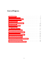
List of Figures
2.1
2.2
2.3
2.4
2.5
2.6
2.7
2.8
2.9
MICAz mote . . . . . . . . . . .
MTS420cc Sensor Board . . . . .
MIB520CB Programming Board .
Structure of IEEE 802.15.4 . . . .
ZigBee Structure . . . . . . . . .
NesC, Modules and Configuration
Dipole Antenna . . . . . . . . . .
Dipole Radiation Pattern . . . . .
Potential Divider . . . . . . . . .
.
.
.
.
.
.
.
.
.
.
.
.
.
.
.
.
.
.
5
6
6
7
8
8
10
10
12
3.1
3.2
RSSI value vs RF Power . . . . . . . . . . . . . . . . . . . . . . . . . . .
Pressure Acquisition Sequence . . . . . . . . . . . . . . . . . . . . . . . .
14
21
4.1
4.2
4.3
4.4
4.5
4.6
A11535 Bandpass Filter, Test Circuit . . . . . .
LTC5507 Block Diagram . . . . . . . . . . . .
LTC5507 Evaluation Board Diagram . . . . . .
LTC5507 Test Circuit Diagram . . . . . . . . .
AZV393 Test Circuit Diagram . . . . . . . . .
Controlled Airspace Boundary Detector Circuit
.
.
.
.
.
.
23
24
25
26
27
28
B.1 TinyOS radio stack for cc2420 . . . . . . . . . . . . . . . . . . . . . . . .
B.2 Picture of the prototype on a breadboard . . . . . . . . . . . . . . . . . . .
45
46
ix
.
.
.
.
.
.
.
.
.
.
.
.
.
.
.
.
.
.
.
.
.
.
.
.
.
.
.
.
.
.
.
.
.
.
.
.
.
.
.
.
.
.
.
.
.
.
.
.
.
.
.
.
.
.
.
.
.
.
.
.
.
.
.
.
.
.
.
.
.
.
.
.
.
.
.
.
.
.
.
.
.
.
.
.
.
.
.
.
.
.
.
.
.
.
.
.
.
.
.
.
.
.
.
.
.
.
.
.
.
.
.
.
.
.
.
.
.
.
.
.
.
.
.
.
.
.
.
.
.
.
.
.
.
.
.
.
.
.
.
.
.
.
.
.
.
.
.
.
.
.
.
.
.
.
.
.
.
.
.
.
.
.
.
.
.
.
.
.
.
.
.
.
.
.
.
.
.
.
.
.
.
.
.
.
.
.
.
.
.
.
.
.
.
.
.
.
.
.
.
.
.
.
.
.
.
.
.
.
.
.
.
.
.
.
.
.
.
.
.
.
.
.
.
.
.
.
.
.
.
.
.
.
.
.
.
.
.
.
.
.
.
.
.
.
.
.
.
.
.
.
.
.
.
.
.
.
.
.
.
.
.
.
.
.
List of Tables
3.1
3.2
3.3
GPS Drivers, filename changes . . . . . . . . . . . . . . . . . . . . . . . .
Leadtek baud rate code . . . . . . . . . . . . . . . . . . . . . . . . . . . .
uBlox baud rate code . . . . . . . . . . . . . . . . . . . . . . . . . . . . .
19
19
20
4.1
4.2
4.3
LTC5507 Tests. 2 MHz . . . . . . . . . . . . . . . . . . . . . . . . . . . .
LTC5507 Tests. 200 KHz . . . . . . . . . . . . . . . . . . . . . . . . . . .
Voltage Comparator Truth Table . . . . . . . . . . . . . . . . . . . . . . .
25
25
26
5.1
Input and Power Measuring stage test results at 0dBm . . . . . . . . . . . .
30
B.1 dBm to mW conversion chart . . . . . . . . . . . . . . . . . . . . . . . . .
44
x
Chapter 1
Introduction
1.1
Introduction
This dissertation is an attempt to design a warning system which would alert pilots of
light aircraft that they are approaching controlled airspace. Currently, controlled airspace
is marked on maps and pilots must plot their courses accordingly. Sometimes, though, the
pilots of light aircraft can lose their way and stray into the controlled airspace of an airport [1, 2]. This can lead to dangerous situations where a light aircraft crosses the paths of
large commercial jet aircraft with the consequent risk of a collision.
The problem of controlled airspace infringement has grown over time for two reasons.
Growth in the commercial aviation sector is the main reason. It leads to the reclassification of
more airspace as controlled airspace when major airports expand their capacity. The second
reason is growth in the number of light aircraft in use.
In the period from 1996 to 2006, there were an average of 389 airspace infringements per
year in the UK [3]. In the Republic of Ireland, figures for airspace infringements are reported
per 100,000 aircraft movements. From 2006 to 2009 an average of 5.75 infringements per
100,000 movements occurred [1]. Given that there were an average of 304,000 movements
each year, then at least 15 airspace infringements happened each year [4].
Each infringement event brings with it (i) the risk of a mid air collision and (ii) an economic impact through delays caused by runway closures while the infringing aircraft exits
the controlled airspace.
In this project two approaches to solving the problem of controlled airspace infringment
were considered. The initial approach consisted of simulating an aircraft and an airspace
boundary marking beacon using MICAz motes.
The second approach involved building a detector capable of detecting the signal from
the VHF Omnidirectional Range navigation system present at all major airports. The signal
strength of this navigation system could then be used to decide if an aircraft was approaching
too close to the airport.
1
1.2
Research Goals
The goal of this project is to produce a proof of concept version of a Controlled Airspace
Boundary Detector for light aircraft. The two main properties the detector must have are:
• The detector must provide adequate warning to the pilot of an aircraft when it detects
the presence of a signal indicating that there is controlled airspace ahead.
• The detector must be simple, contain very few components and need very little power.
The first requirement is the most important requirement for both a proof of concept device
and a commercially produced device. Simplicity is a requirement of all devices on aircraft to
avoid adding to a pilot’s workload. The device needs to have a small component count and
need little power so that it can be fitted to aircraft with even the most stringent weight and
power limits.
1.3
Structure
This chapter has covered the motivations for the project and the research goals.
Chapter 2 gives an overview of the state of the art. It includes an overview of the definitions of various types of controlled airspace and an overview of the transmission technologies used by the aviation sector. It also describes the basics of antennas and discusses the
hardware and software used in the project.
Chapter 3 covers the initial prototype research using MICAz motes and TinyOS.
Chapter 4 describes in detail the demonstration system built using dedicated hardware.
It gives a detailed explanation of each component of the detector and an overview of the
completed detector.
Chapter 5 discusses tuning the assembled system and the results of testing the system.
Chapter 6 draws conclusions and discusses some possible future work which would improve the detector.
The appendices contain code listings etc.
2
Chapter 2
Background
This chapter presents an overview of the regulations, technologies and physics which underlie the design and implementation of a proof-of-concept Controlled Airspace Boundary
Detector. It begins with some definitions related to controlled airspace and the transmission technologies used at airports. Then the motes used in the early prototyping stage are
discussed in detail along with their communication protocol, (ZigBee) and the software running on them, (TinyOS and NesC). The final sections of the chapter provide a brief overview
of the Global Positioning System (GPS) and the physics of antennas and circuits.
2.1
Controlled Airspace
Controlled airspace is divided up into a number of classes, A to G [5], by the International Civil Aviation Authority (ICAO) [6]. Each country has definitions for their controlled
airspace which closely follow these international guidelines. In Ireland all airspace falls into
one of the three classes A, C or G [7].
The airspace around an airport is broken into three zones. At the center is the Control
Zone (CTR). In Ireland this is generally a cylinder with a radius of 15 nautical miles and a
height from the ground of 2,500 feet [8]. Above the Control Zone, and extending beyond
it, is the Control Area (CTA). The control area extends from a specified lower altitude to a
specified upper altitude. The CTA can be any shape but is often a rectangular box aligned
with the runways at the airport. In Dublin airport for example the upper limit is 24,000
feet [9]. In Ireland the CTR and CTA zones correspond to class C of the ICAO airspace designations [5, 7]. The final zones are called Air Traffic Service (ATS) routes. These are routes
of controlled airspace, usually between airports [9]. ATS routes define the path between
airports and include specifications such as the minimum safe altitude on the route.
There are a number of other types of airspace which are less common, including danger
area, prohibited area and restricted area [5]. These special areas surround various military
or civilian sites of a high security nature, such as nuclear power plants and military bases.
3
2.2
Transmission Technologies
There are a large number of electromagnetic transmission technologies used at all modern
airports. These include communications radios at Very High Frequency (VHF) and High
Frequency (HF), navigation aids such as instrument landing systems (ILS), and monitoring
systems such as radar.
Airports use a large number of HF and VHF bands for communication with aircraft. HF
radio reserved for use by airports in Ireland is at frequencies between 2MHz and 10MHz, and
VHF radio at frequencies between 108MHz and 140MHz [10, 11]. These frequency bands
are divided between communication, navigation and monitoring uses.
Radar is used at airports for determining the velocity and position of aircraft. All airports
have both primary and secondary radar systems. Primary radar works by detecting reflected
pulses of radio waves. It is used to calculate the position and velocity of the aircraft which
the beam intercepts. Secondary radar systems interrogate the aircraft they detect using a
pulsed signal. All large aircraft carry a transponder which responds to the pulses with an
identification code [12]. Secondary radar transmits at a frequency of 1030MHz and replies
are sent by aircraft at 1090MHz [10, 13, 14].
Navigation aids at airports come in two forms: short range systems such as Instrument
Landing System (ILS) and long range systems such as Very High Frequency Omni directional Range (VOR).
VOR provides navigation beacons along the ATS routes between airports [15]. VOR
works by encoding the azimuth (angle to a station) in the phase relationship between a variable and a reference signal. The variable signal rotates at 1800 r.p.m. [16], and its phase
varies in phase with its azimuth angle. The reference signal phase is constant at all azimuth angles. Bearings calculated using the system are relative to magnetic north [16]. VOR
uses frequencies between 108 and 118MHz [16, 17], and has a typical range of 100 nautical
miles [18].
Distance measuring equipment (DME) is usually co-located with VOR. It allows aircraft
to calculate their distance from the ground station by timing the interval between sending out
a series of pulses and receiving a corresponding sequence of pulses in reply [17].
2.3
MICAz Motes
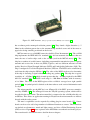
In this section, the MICAz wireless sensor systems (developed by Crossbow [19], and now
owned and produced by MEMSIC [20]) are described in detail. Areas described include
the antenna, the radio chip and the micro controller. Figure 2.1 shows a picture of a typical
MICAz mote.
By default, a MICAz mote is equipped with a λ4 antenna [22,23]. The antenna is a simple
monopole, (described in Section 2.7) and takes the form of an insulated length of wire.
In [23], Su et al. present the results of an investigation of the propagation characteristics of
MICAz motes. Their measurements of the radiation pattern of the mote antenna show that it
4
Figure 2.1: MICAz mote. (Image reproduced from MICAz user manual [21])
has an almost perfect monopole radiation pattern [23]. They found a slight distortion (< 5
dBm) in the radiation pattern due to the antenna being attached at one end of the mote as
opposed to being centrally positioned on the device.
MICAz motes use a cc2420 RF transceiver built by Texas Instruments [21]. The cc2420
chip implements the IEEE 802.15.4 standard [24], and can transmit data at more than ten
times the rate of earlier chips such as the cc1000 (used in the MICA2 mote) [25]. The
chip has a number of useful features, including programmable transmission power, separate
transmit and receive first in first out (FIFO) registers, and two different measures of link
quality, Received Signal Strength Indicator (RSSI) and Link Quality Indication (LQI). The
chip is configured via a Serial Peripheral Interface (SPI) bus. The RSSI can be continuously
read from the chip using the SPI bus [22]. The value of the RSSI can be used to determine
if the chip is detecting a signal without decoding any packets [22]. The chip has a typical
sensitivity of −95 dBm [22], which is much greater than the −85 dBm required by the IEEE
802.15.4 standard [24]. The RSSI’s total range is −100 dBm to 0 dBm, with an accuracy
of ±6 dBm. The value in the RSSI register of the cc2420 is averaged over eight symbol
periods [22]. A symbol period is defined as the time taken to send a unit of information such
as a byte.
The microcontroller on the MICAz is an ATmega128 8-bit RISC processor manufactured by ATMEL [26]. The ATmega128 runs the TinyOS operating system, which will be
described in the next section. The microcontroller is connected to the cc2420 radio chip via
an SPI bus. This allows an application running in TinyOS on the microcontroller to interact
directly with the radio system.
The mote’s capabilities can be expanded by adding plug-in sensor boards [27]. Sensor
boards can be used to add a large number of additional functions to a mote. These functions
can include accelerometers, sound and light sensors, and also a Global Positioning System
(GPS) receiver. Figure 2.2 shows a picture of the MTS420cc sensorboard used in this project.
The sensorboard is described in more detail in the next chapter.
5
Figure 2.2: MTS420cc Sensor Board
Figure 2.3: MIB520CB Programming Board (Image reproduced from MICAz user manual [21]
Programming of the MICAz motes is done using the MIB520CB USB Interface Board
described in the MPR/MIB manual [21]. In the Linux system used throughout this project,
the programming board is recognised as a USB (Universal Serial Bus) device. It is assigned
an identifier such as /dev/ttyUSB2 where the number depends on how many USB devices
are connected to the computer.
2.4
ZigBee and IEEE 802.15.4
IEEE 802.15.4 is a wireless communication standard for personal area networks. It defines
the physical and medium access control layers. ZigBee is an implementation of two transport
layers, (network (NWK) and application (APL)) on top of IEEE 802.15.4 [28, 29]. ZigBee
has the same relationship to IEEE 802.15.4 as WiFi has to IEEE 802.11. Figure 2.5 illustrates
how ZigBee and IEEE 802.15.4 fit together.
The physical layer of IEEE 802.15.4 supports three different frequency bands, including
the 2.4GHz industrial, scientific and medical (ISM) band [24]. The PHY layer uses Direct
6
Figure 2.4: Structure of IEEE 802.15.4
Sequence Spread Spectrum (DSSS) as an access mode, with Offset Quadrature Phase Shift
Keying (O-QPSK) as its modulation [28]. The PHY layer is illustrated in Figure 2.4.
The MAC layer of IEEE 802.15.4 supports a slotted carrier sense multiple access - collision avoidance (CSMA-CA) protocol. Two types of device are possible - full function
devices (FFD) and reduced function devices (RFD). The difference between an FFD and
RFD is that an FFD can act as a network controller whereas a RFD can only be an end
device [28, 29]. The MAC layer is illustrated in Figure 2.4.
The ZigBee network layer is designed to provide support for multi-hop routing [29]
across networks with an arbitrary arrangement of FFD and RFD devices. ZigBee’s application layer is designed to provide support for the development and deployment of distributed
programs [28]. ZigBee specifies three different device types an end device, a router and a
coordinator. These are illustrated in figure 2.5. These three device types can be used to create
a multitude of network topologies [28]. The ZigBee end device is equivalent to an RFD. A
router or coordinator node is an FFD at the lower layer.
The application layer of ZigBee specifies a number of parts - ZigBee Device Objects
(ZDO), the Application Sub Layer (APS) and Application Objects (APO) [28]. The APOs
are user-defined modules which add functionality to a particular system. The APOs on a
particular deployment use the network service and device discovery interface provided by
a device’s ZDO to perform their programmed functions [28], [29]. The APS talks to the
network layer of the ZigBee deployment.
2.5
TinyOS and NesC
TinyOS is an operating system designed for use on embedded systems [30]. TinyOS is
written in the NesC language. NesC stands for Networked Embedded Systems C [31]. NesC
is a variant of the C programming language. It allows developers to create modules which
encapsulate basic functionality such as blinking the Light Emitting Diodes (LEDs) on a mote.
The TinyOS system is available for a number of platforms including Microsoft Windows and
Linux [30]. In this project, TinyOS was installed on a computer running Ubuntu Linux 10.04.
The goal of NesC is to allow a modular style of programming while using much of the
7
Figure 2.5: ZigBee Structure
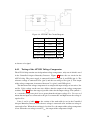
Figure 2.6: NesC, Modules and Configuration
syntax of the C programming language. All functionality in TinyOS is provided in the form
of components. Components come in two forms - modules and configurations. Modules
provide interfaces consisting of events and commands. To call the commands provided by
an interface a module must implement all of the events provided by the interface. Configurations are a special type of component which connect the modules using an interface to the
modules providing the interface. These connections are called wiring [31] and allow compile
time checking of all possible code execution paths. To provide an interface, a module must
implement the commands defined by an interface and signal the events. Figure 2.6 shows an
overview of NesC. A module providing two interfaces is represented with triangles pointing
out of a rectangle. A module using an interface is represented with a triangle pointing into
the rectangle. The lines joining the user to the provider represent the wiring done in the
configuration. Appendix A shows a listing of the code from the Blink tutorial [32] which
will be discussed further in chapter 3.
When the modules of an application are wired together with the necessary hardware
components provided by TinyOS to form an application the result compiles to a single executable. This executable is then loaded to the hardware, usually a mote, using a customized
GNU toolchain provided with the TinyOS system [32].
The TinyOS system provides a task queue to which application programmers can post
8
tasks with the post command. Tasks in the TinyOS system cannot preempt each other; however, a hardware interrupt can preempt an executing task [33]. Only one instance of a task
can exist on the task queue; however, once a task begins executing it is no longer part of the
queue and can be reposted to the task queue. This behaviour allows a task to remain alive on
a permanent basis.
2.6
Global Positioning System
The Global Positioning System is a satellite navigation system developed by the United
States military in the 1960’s and 70’s [34]. It consists of a constellation of 24 satellites in orbit
around the earth [35]. Each satellite in the constellation transmits signals containing a precise
time generated by an atomic clock [34], along with information about the satellite’s orbital
parameters. Receivers on the ground including the GPS receiver on the MTS420cc sensor
board, use the signals from at least 4 satellites to calculate their position and altitude [36].
The receiver calculates its own position by finding the intersection of 4 spheres defined
by the received signals. The radius of the spheres is calculated as follows. Each signal
contains the transmission time of the signal ti where i is the number of the satellite, 1 to
4. tr is the received time of the signal at the receiver. The radius of any sphere is given by
(tr − ti )c where c is the speed of light (3 × 10⁸ ms−1 ). Two spheres will intersect at either
a point or a circle. (The case of two spheres not intersecting is not relevant for the GPS
system.) The third sphere calculated will intersect the point or circle intersection of the first
two at a maximum of two points. Calculation of the fourth sphere allows the correct position
from the 3-sphere calculation to be selected. This is usually the point closest to the earth’s
surface [36].
2.7
Antennas
At a fundamental level, an antenna is a device which converts electrical waves in a wire to
radiating waves in free space. All electromagnetic phenomena are described by Maxwell’s
equations [37]. These fundamental laws basically state that only accelerating electric charges
produce electromagnetic waves. The goal of all antenna design is to make the process of
generating electromagnetic waves from accelerating electrons as efficient as possible.
There are a large number of antenna designs, the most basic type being a center-fed dipole
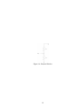
antenna [38]. The simplest center fed dipole is made from two pieces of straight wire. Figure
2.7 illustrates a typical arrangement for a center fed dipole antenna. The signal generator is
connected to the centre of the dipole and the electric fields in the two halves of the dipole
add to produce a lobe shaped radiation pattern. In three dimensions it is seen that a dipole
antenna produces a torus shaped radiation pattern [38]. The torus is in a plane perpendicular
to the axis of the dipole as illustrated in Figure 2.8.
Other antenna types include monopole antennas, parabolic dish antennas, loop and he9
Figure 2.7: Dipole Antenna
Figure 2.8: Dipole Radiation Pattern
10
lical antennas. Horn antennas are used for high frequency (> 1GHz) applications. Patch
antennas, which are printed on circuit boards, are used where compact size is a requirement [38].
The Friis formula relates the power transmitted to the power received:
λ 2
Pr
= Ga Gb
Pt
4πr
(2.1)
Where Ga , Gb are the gain of the transmitter and receiver, respectively, λ is the wavelength
of the radiation, and r is the distance between transmitter and receiver. Pr and Pt are the
received and transmitted powers, respectively.
The gain is related to the geometric shape of an antenna. This relationship is called the
aperture of the antenna.
4π
(2.2)
G = 2 Ae
λ
Where Ae is the aperture of the antenna. The aperture is easy to visualize in the case of a
dish antenna (it is simply the diameter), but is applicable to all types of antenna [38].
2.8
Review of basic circuit theory
This section presents a brief overview of some basic equations used in circuit calculations.
These equations are used extensively in chapter 4 which covers the design of the final experimental system.
The most basic equation is Ohm’s law, which states that the voltage (V ) is equal to the
current (I) flowing in a conductor times the resistance (R) [37].
V = IR
(2.3)
The power (P) produced in a conductor by a current I can be shown experimentally to
obey the following law [37].
P = RI 2
(2.4)
For solving problems involving complete circuits, Kirchoff’s laws are indispensable. Kirchoff’s first law states that current splits at a junction in a circuit and that the total current
entering the junction must be equal to the total current leaving the junction. Kirchoff’s voltage law states that in a closed loop the sum of the voltage drops must be equal to the voltage
of the power supply.
A potential divider, which consists of a pair of resistors, can be used to obtain a lower
voltage from a high voltage supply. Figure 2.9 shows a typical potential divider. The power
supply is connected to Vin and the ground terminal. The output is measured between Vout
and the ground terminal. The output voltage is calculated from the equation
Vout =
R2
Vin
R1 + R2
11
(2.5)
Figure 2.9: Potential Divider
12
Chapter 3
Mote Development
Initial work in this project was aimed at developing a mote based proof-of-concept Controlled Airspace Boundary Detector. To build a demonstration version using MICAz motes,
a number of problems were identified which needed to be solved. Firstly, to simplify initial
detection of a boundary marking signal, the RSSI value detected by the mote would have to
monitored for significant changes. Secondly, the position and velocity of the mote representing the aircraft would have to be determined from the GPS sensor. Thirdly, the altitude of
the mote would have to be determined either from the GPS sensor or from the barometric
pressure sensor on the MTS420 sensor board [39]. This chapter describes all three of these
areas in detail, and concludes with a discussion of the reasons for building the demonstration
system described in chapter 4.
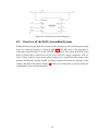
3.1
Reading the RSSI register
The RSSI (Received Signal Strength Indicator) register on the cc2420 stores an 8-bit value
representing the average signal strength over the last eight symbol periods [22]. When the
chip is initially powered on, the RSSI value is inconsistent until the first eight symbol periods
have elapsed. No hardware level setup or configuration is required to activate the RSSI
register. Figure 3.1 shows a graph of the RSSI value verses the Radio Frequency (RF) input
power. The graph demonstrates that the relationship between the two is close to linear.
Initial work towards reading the RSSI register of the cc2420 chip using TinyOS consisted
of reading the TinyOS tutorials, the TinyOS programming manual and the TinyOS Enhancement Proposals (TEPs) [31, 40, 41]. A number of useful features of the TinyOS system were
identified as a result of this work. Firstly, a number of demonstration programs provided
with the TinyOS system could be adapted for our work with little or no modification. These
included the BaseStation application and the SendingMote application. Secondly, the presence of a debugging library and PC-based receiver program which uses it were identified.
Finally, based on reading the tutorials, programming manual and TEP 126 (which describes
the TinyOS cc2420 radio stack implementation), it became clear that the RSSI register should
be accessed through the CC2420ControlC component.
13
Figure 3.1: RSSI value vs RF Power (Image reproduced from cc2420 manual [22])
3.1.1
First attempt to read the RSSI register
The Blink demonstration application provided with the TinyOS system (See Appendix A.1
for the source code) was studied to gain familiarity with the NesC language and TinyOS. The
application originally blinked the three LED’s on the MICAz mote (see figure 2.1); the code
shown in appendix A.1 has been reduced to blinking one LED for space-saving reasons. The
application was successfully installed on a mote using the following commands
make micaz
make micaz reinstall mib520,/dev/ttyUSB0
which verified that the TinyOS system was correctly installed and configured as per the
instructions in the tutorial [32].
The RSSI demo provided as part of the TinyOS system, and discussed in the RSSI demo
tutorial [42], extracts the RSSI value from the headers of packets received by a mote. For the
purposes of this project a simpler approach of directly reading the RSSI register was chosen.
To achieve this, the ReadRSSI application listed in Appendix A.2 was created. It follows the
instructions from the TinyOS programming manual, which lists the steps below as necessary
for activating the cc2420 radio chip from TinyOS.
1. Turn on the voltage regulator
2. Acquire the SPI bus to the radio
3. Start the radio’s oscillator by sending a command over the bus
4. Put the radio in RX (receive) mode
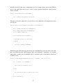
Reading of the RSSI register was done using the read interface which the CC2420ControlC
component of the TinyOS radio stack implementation (see figure B.1), provides for the register.
The startup sequence of the radio is initiated in the booted event by a method call to start
the radio’s voltage regulator. The subsequent steps of the chain are initiated in the event
14
handlers for the previous step’s completion event. For example when control of the SPI bus
passes to the application, the resource-granted event is signaled which kicks off the starting
of the oscillator.
event void Resource.granted()
{
call Power.startOscillator();
}
The final event in the chain is the startOscillator event which places the application in the
started state.
async event void Power.startOscillatorDone()
{
call Fifo.enableFallingEdge();
call Sfd.captureRisingEdge();
call Power.rxOn();
call Resource.release();
//Change state to started
atomic
{
state = STATE_STARTED;
}
}
When the application enters the started state, the event handler for the timer-fired event calls
the read command on the RSSI register. This read command is split-phase, so it returns
immediately, and the value of the RSSI register is returned by the system when it signals the
readDone event.
event void Read.readDone(error_t result, uint16_t val)
{
if ( result == SUCCESS )
{
printf("\t\t%d\n", val);
}
else
{
printf("failed to read rssi\n");
}
printfflush();
}
15
The readDone event sends the RSSI value to the PC over the serial line using the printf
debugging library. The PC must have the PrintfClient java application (which is provided
with the TinyOS system) running to receive the printed values [43].
Testing of the ReadRSSI application was performed by loading a second mote with the
SendingMote demo program which is part of the RSSI tutorial [42]. The SendingMote application simply broadcasts an empty packet periodically. This empty packet should have
been occasionally detected and shown as a high value in the RSSI values being printed on
the PC screen. The result, however, was that the RSSI value would increase and then fail to
be subsequently updated by the hardware.
Three potential causes were identified based on a careful reading of the cc2420 manual.
The three potential causes identified are
• Address Recognition possibly leaving the SFD (start frame delimiter) pin in the wrong
state.
• No receiver for the incoming packets.
• RX (Receive) buffer not flushed.
Each probable cause was investigated in succcession, but was eliminated without a positive
result. Resetting the SFD pin had no effect, attaching a dummy receiver prevented any
increase in the RSSI value. and flushing the RX buffer also had no effect.
3.1.2
Second attempt to read the RSSI register
Based on advice from another researcher and because of the unlikelihood of isolating the
underlying bug within the time constraints of the project, a complete rewrite was performed.
In the second version it was decided to use a high level component of the TinyOS radio stack
ActiveMessageC to start the radio. See appendix A.3 for a complete listing of the code. The
reading of the RSSI register was triggered every 50ms by a timer and was carried out in a
similar fashion to the first version of the program, by using the ReadRSSI interface of the
CC2420ControlC component.
Testing of this new version of the program revealed that it worked as expected (high
values of RSSI when a packet was being received, and low values at all other times). The
author suspects that the source of the error in the first version of the code was related to the
handling of the SFD captured event. Extensive reading of the source code of the TinyOS
radio stack did not, however, lead to a full understanding of the cause of the problem.
Appendix A.4 shows another version of the ReadRSSI application which uses a task to
read the RSSI register. This minor rewrite of the code performs exactly the same as the timerbased version described in this section. This task-based version of the code would however
be more readily extensible to incorporate other sensors such as the GPS sensor discussed in
the next section.
16
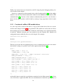
3.2
GPS Driver
With the code for reading the RSSI working, attention was focused on getting the position of
the mote from the GPS sensor on the MTS420 sensor board. The MTS420CC sensor board
uses a uBlox LEA-4A GPS module [44]. The earlier CA and CB versions of the MTS420
board use a Leadtek GPS-9546 module. Examination of the TinyOS system showed that
there was no driver supplied for the MTS420 sensor board. An online search located a driver
for the CA version of the board, developed by the Rincon Corporation and available freely
on the TinyOS repository [45, 46].
3.2.1
Testing of the Leadtek driver
The Leadtek driver, which, as described above, was designed for earlier versions of MTS420
sensor boards, was tested on the CC version of the board. It failed to operate the uBlox
GPS module. Testing was performed by running the TestNmeaParse application provided
with the Leadtek driver on a mote with the MTS420 sensorboard and GPS antenna attached.
During the test, a modified version of the BaseStation application was running on a mote
connected to the PC. This BaseStation application was modified to allowing decoding of the
GPS packets sent by the TestNmeaParse application on the first mote. The BaseStation code
was modified in a number of ways. Firstly, the definition of the NMEA packets was added,
static nmea_gga_msg_t *gpsPkt; //Incoming gps data
then the receive event was modified to act only on the reception of GPS packets.
event message_t *RadioReceive.receive[am_id_t id](
message_t *msg,
void *payload,
uint8_t len) {
if (len == sizeof(nmea_gga_msg_t)) {
gpsPkt = (nmea_gga_msg_t *)payload;
printf("lat %d %d %c",
gpsPkt->latitude.degree, gpsPkt->latitude.minute,
gpsPkt->latitude.direction);
printf(" long %d %d %c",
gpsPkt->longitude.degree, gpsPkt->longitude.minute,
gpsPkt->longitude.direction);
printf(" alt %d\n", gpsPkt->altitude);
printfflush();
}
return msg;
17
}
Finally, the decoded data was forwarded to the PC using the printf debugging library discussed earlier in this chapter.
Based on a comparison of the manual for the older Leadtek module [47] and the uBlox
module, it was discovered that both modules adhered to the NMEA 0183 standard for GPS
communication [48]. Because of the common communication protocol, it was felt that a
driver for the uBlox module could be built by reusing a large proportion of the Leadtek
driver.
3.2.2
Creation of a uBlox GPS module driver
As a first step in the creation of the driver, a copy of the Leadtek driver files was created,
and the name changes in table 3.1 were performed. Files which are used by the new driver
but not changed are not listed in the table. Numerous small changes were required internally
in each file. Modules using the files were updated to use the renamed files. Module and
configuration names within the files were also adapted. For example,
configuration gps9546C {
becomes
configuration gpsUbloxLea4aC {
The next step in the driver development process was to examine the parts of the code where
the hardware settings are specified, such as this segment (from Nmea.h [46])
enum {
NMEA_START = 0x24,//$
//NMEA_END1 = 0x0D,//CR
NMEA_END = 0x0A,//LF -- NMEA ’sentence’ terminator
NMEA_DELIMETER = 0x2C,//’,’
NMEA_CHECKSUM_DELIM = 0x2A,//’*’
ASCII_PERIOD = 0x2E,//ASCII period ’.’
ASCII_ZERO = 0x30,//ASCII zero ’0’
ASCII_FIVE = 0x35,//ASCII five ’5’
ASCII_NINE = 0x39,//ASCII nine ’9’
ASCII_A = 0x41,//ASCII ’A’
ASCII_G = 0x47,//ASCII ’G’
ASCII_M = 0x4D,//ASCII ’M’
ASCII_P = 0x50,//ASCII ’P’
};
and modify them to match the specifications mentioned in the uBlox manual [44]. In the
case of the above segment the third line was uncommented to match the specifications of
18
Leadtek GPS-9546
uBlox LEA-4A
HplGps9546C.nc
HplGpsUbloxLea4aC.nc
HplGps9546P.nc
HplGpsUbloxLea4aP.nc
gps9546C.nc
gpsUbloxLea4aC.nc
gps9546P.nc
gpsUbloxLea4aP.nc
Table 3.1: GPS Drivers, filename changes
implementation {
atm128_uart_config_t c4800 = {//NMEA standard
ATM128_UART_BAUD_4800,
ATM128_UART_CLOCK_DOUBLE,
ATM128_UART_CHARSIZE_8,
ATM128_UART_PARITY_NONE,
ATM128_UART_STOPBITS_1,
};
command error_t StdControl.start(){
if(call UartControl.start() == SUCCESS) {
call UartConfig.setConfig(&c4800);
return SUCCESS;
} else {
return FAIL;
}
}
Table 3.2: Leadtek baud rate code
the NMEA packet sent by the uBlox module. Testing of the modified code showed that
it still failed to successfully control the GPS module. This testing was performed using
a slightly modified version of the TestNmeaParse application used previously to test the
Leadtek driver. The application was modified so that it used the uBlox components under
development, instead of the Leadtek driver components.
Further online research located a paper by Silva et al. [49], who claimed to have developed a driver for the MTS420CC sensorboard. In the paper they mention making several
changes, including changing the baud rate. This change had not been attempted in our work
due to the uBlox module datasheet mentioning a number of baud rates, including the baud
rate originally used in the code.
The baud rate settings in the code were modified from that shown in table 3.2 to the settings shown in table 3.3. The TestNmeaParse application was then recompiled and reloaded
onto a mote. The changes to the code had the desired effect and GPS coordinates were received on the PC. During testing it was noted that the figure given in the uBlox manual for
a cold start is inaccurate. The manual gives 41 seconds as the maximum startup time. Re19
implementation {
atm128_uart_config_t c9600 = {
ATM128_UART_BAUD_9600,
ATM128_UART_CLOCK_DOUBLE,
ATM128_UART_CHARSIZE_8,
ATM128_UART_PARITY_NONE,
ATM128_UART_STOPBITS_1,
};
command error_t StdControl.start() {
if(call UartControl.start() == SUCCESS) {
call UartConfig.setConfig(&c9600);
return SUCCESS;
} else {
return FAIL;
}
}
Table 3.3: uBlox baud rate code
peated cold starts of the mote/sensorboard combination showed that the average startup time
was close to two minutes. It was also noted that the altitude reported by the GPS module
varied widely on a timescale of minutes.
3.3
Measuring Altitude with a Pressure Sensor
Since the altitude returned by the uBlox GPS module was not accurate enough for use in
even a demonstration system it was decided to use the Intersema MS5534 pressure sensor
on the MTS420 as an altimeter [39, 50]. An altimeter makes use of the relationship between
pressure and depth in a gas to calculate the height above sea level. In an incompressible fluid
like water, the relationship between pressure and depth is P = ρgh where ρ is the density
of the fluid and g is the acceleration due to gravity at the surface of the earth (9.81ms−2 ).
For mixtures of gases like air, the relationship between pressure P and height h is more
complicated because the density varies as the pressure varies. The relationship is given by
h = cT ln
P
P0
where P0 is the pressure at sea level, P is the measured pressure, T is the temperature and c
is a constant related to the molecular properties of the gas [37].
Given the lack of any driver for the pressure sensor, initial work on building a driver
focused on understanding (a) how the pressure sensor is wired on the MTS420 sensorboard
and (b) the communication protocol it expects. The MTS420 documentation [39] shows the
20
Figure 3.2: Pressure Acquisition Sequence (Image reproduced from MS5534 manual [50])
pressure sensor as being connected to the USART1 hardware interface of the MICAz mote’s
processor [26]. This is the same interface that the GPS sensor discussed in the last section,
is connected to. A comparison of the communication protocol expected by the MS5534
pressure sensor and the capabilities of the USART1 interface revealed a fundamental incompatibility [26, 50]. The pressure sensor requires that each instruction sent to the device is
followed by two further ticks of the serial clock line. This is shown in figure 3.2, which
shows the timing diagram for reading the pressure from the sensor. To control the number
of ticks of the clock, the ATMega128 datasheet implies that the USART hardware should be
placed in a synchronous clock operation mode. (See pg. 175 of [26].) The datasheet does not
make it clear, however, whether the synchronous mode will produce clock ticks only if data
is being transmitted. Investigation of the TinyOS driver code for the USART system showed
that it only implements the asynchronous operation mode. The imprecise information on the
USART and the need to reimplement a core part of the TinyOS system led to a decision to
build a demonstration system using dedicated hardware. This decision is discussed in detail
in the next section, and a complete description of the hardware is covered in chapter 4.
3.4
Summary of the limitations of the Mote Prototype
A number of important limitations of mote based prototyping were identified as the work
described in this chapter progressed. These limitations are:
• The frequency which the motes operate at is unlicenced and also ZigBee is a short
range communication system. These factors made it ideal for building a proof of
concept system. A real system, however would have to operate in a frequency band
licenced to the aviation industry world wide, such as in the VOR or Secondary Surveillance Radar bands [10].
• The altitude returned by the GPS sensor is not stable enough to be useful.
• The TinyOS driver for the USART interface of the ATMega processor may have to be
reimplemented, to allow reading of the pressure sensor.
Given these limitations a decision was made to build the dedicated hardware described in
chapter 4.
21
Chapter 4
Building Dedicated Hardware
The dedicated hardware is designed to detect the frequencies used by the VOR navigation
system (108-118MHz). It was decided to use these frequencies for two reasons,
1. Part of the operation of the VOR system involves it transmitting a constant signal.
This signal is constant in a radius around the VOR transmitter and so would make any
system detecting it omnidirectional.
2. The strength of the constant signal from the VOR station decays with distance from
the station. This decay rate is proportional to r12 and as such can be used to detect the
distance that the detector is at from the station.
The first section of this chapter gives an overview of the functioning of the dedicated
hardware. Subsequent sections describe the functioning of each component in detail and the
final section describes the fully assembled hardware.
4.1
Overview
The Controlled Airspace Boundary Detector consists of three stages: an input stage, a power
measuring stage and an output stage. The input stage consists of an antenna, and a filter
which removes the frequencies outside the 108MHz to 118MHz range of VOR. The power
measuring stage provides an output voltage proportional to the power of the input signal.
The output stage signals a warning in the form of an LED when the measured signal power
exceeds a predefined threshold.
4.2
Input Stage
The input stage of the Controlled Airspace Boundary Detector consists of an antenna and
an A11535 crystal filter manufactured by Advanced Material Technologies [51]. Crystal
filters exploit Surface Accoustic Waves (SAW) on a quartz crystal to filter incoming signals.
An electrode is attached at each end of the quartz crystal. The signal at the input electrode
22
Figure 4.1: A11535 Bandpass Filter, Test Circuit
excites a SAW in the crystal, and the output electrode converts it back to an electrical signal.
The geometric properties of the crystal (length, width, etc.) determine which frequencies can
pass through the filter [52].
The antenna is a simple monopole antenna as described in section 2.7. It receives the
VOR signal and a large number of other frequencies above and below the VOR frequency
band. The A11535 filter is used to remove the frequencies outside the VOR band.
4.2.1
A11535 Bandpass Filter
The A11535 bandpass filter has a 3dB bandwidth of 4.93MHz centered at 115MHz [51]. It
has a high impedance at all frequencies outside the bandwidth. This allows the VOR frequencies to pass through the filter and removes all other frequencies detected by the antenna.
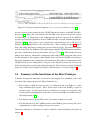
Figure 4.1 shows the circuit used to test the operation of the filter. An RF signal is input at
the RFin terminal. For testing, the input signal is generated by a signal generator. The output
of the filter is measured at the RFout terminal. The values of the inductors L1 and L2 are
56nH and 22nH, respectively, and the capacitor C1 is 39pF.
4.3
Power Measuring Stage, LTC5507
The power measuring stage of the detector is the core of the system. It consists of the
evaluation board for the Linear Technologies LTC5507 RF Power Detector [53], [54]. The
LTC5507 RF power detector consists of a Schottky diode and an amplifier integrated into a
single chip [53].
A diode is an electronic component which conducts current in only one direction. A
Schottky diode is a special form of diode which has a fast switching performance and the
voltage drop across it is very low. Normal diodes consist of two pieces of silicon with
different doping characteristics called p and n type. A Schottky diode is made from a metal
joined to an n-type piece of silicon [55]. For power detection, a Schottky diode is used
in conjunction with a capacitor. In the case of the LTC5507 this capacitor is an external
component [53].
An amplifier is a device which changes the magnitude of a signal. In the LTC5507 power
detector, a buffered amplifier is used. This prevents any interference between the output and
23
Figure 4.2: LTC5507 Internal Block Diagram (Image reproduced from LTC5507 manual [53])
the input.
Figure 4.2 shows a block diagram of the internal components of the LTC5507 power
detector chip. The RF input is connected to the Schottky diodes on the left of the image.
Output from the detector stage is fed into the buffered amplifier on the right of the image,
which is connected to the Vout pin.
4.3.1
Testing of the LTC5507 Evaluation Board
Initial testing of the LTC5507 Evaluation Board was done to verify the accuracy of the output
range claimed in the datasheet [53], and to find the input voltage needed to give the maximum
output. The evaluation board circuit diagram is shown in figure 4.3. The demo board’s
external connections are labeled E1 through E5, and J1. RF signals are supplied to the board
through a co-axial connector at J1. The power supply to the chip is connected between VCC
and GND at E1 and E3. The output voltage is measured between Vout (E2) and GND.
For the initial testing of the LTC5507 demo board, a signal generator was used to supply
the RF signal. This signal generator has a maximum peak-to-peak output of 21.4V, which
exceeds the maximum specifications of the LTC5507 chip. A potential divider is therefore
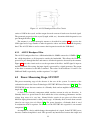
used to limit the maximum voltage. A typical experimental setup is shown in figure 4.4.
The output of the signal generator is connected to a potential divider. The RF input of the
LTC5507 is connected via a co-axial cable to the Vout of the potential divider and the negative
of the signal generator (not shown). The LTC5507 is powered by a direct current (DC) power
supply set to 5.5 volts and connected between E1 and E3. The output of the LTC5507 chip
was measured using an oscilloscope between terminals E2 and E3 of the demo board.
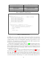
A series of tests were carried out with the voltage supplied to the RF input pin of the
LTC5507 being increased each time. The results of this series of tests is shown in table 4.1.
From the table, the input impedance can be calculated as follows. The output voltage can
24
R1
Ω±5%
560
390
180
120
R2
Ω±5%
68
68
68
68
Potential Divider
Vout ±0.1V
2.2
2.8
4.8
5.8
LTC5507
Vout ±0.02V
1.05
1.25
1.95
2.25
Power
dBm±1
3
5
12
13
Impedance
Ω ± 100
2400
1900
1500
1300
Table 4.1: LTC5507 Tests. 2 MHz
R1
Ω±5%
560
390
180
120
R2
Ω±5%
68
68
68
68
Potential Divider
Vout ±0.1V
2.2
2.8
4.8
5.8
LTC5507
Vout ±0.02V
0.70
0.76
0.92
1.10
Power
dBm±1
-4
-2
1
3
Impedance
Ω ± 1000
12000
12000
18000
17000
Table 4.2: LTC5507 Tests. 200 KHz
be converted to input power using the graphs in the LTC5507 datasheet [53]. Taking the
final output voltage of 2.25 volts, and using the datasheet, the input power is found to be
∼ 13dBm. Using the input voltage of 5.8V, equation 2.4, and converting 13dBm to 20mW,
gives an input impedance of ∼ 1300Ω.
Tables 4.1 and 4.2 show the results of testing the LTC5507 chip at 2MHz and 200kHz,
respectively. It can be seen that the impedance of the chip is an order of magnitude higher
at the lower frequency. The variation in input impedance with frequency means that the
potential divider must be changed to achieve the same input power at different frequencies.
As the frequency decreases, the input RF voltage must be increased to maintain the same
measured power level by the LTC5507 chip.
4.4
Output Stage
The output stage of the Controlled Airspace Boundary Detector consists of an AZV393 dual
voltage comparator manufactured by BCD Semiconductor, and an LED [56]. The purpose
of the output stage is to convert the measurements performed by the power measuring stage
into a simple visual indicator of an LED lighting, or not lighting, depending on the presence
Figure 4.3: LTC5507 Evaluation Board Circuit Diagram
25
Figure 4.4: LTC5507 Test Circuit Diagram
In -
In +
Output
<
Vref
high
>
Vref
low
Vref
<
low
Vref
>
high
Vref
Unconnected
high
Unconnected
Unconnected
low
Table 4.3: Voltage Comparator Truth Table
or absence of a signal.
4.4.1
Testing of the AZV393 Voltage Comparator
The AZV393 chip contains two independent voltage comparators, only one of which is used
in the Controlled Airspace Boundary Detector. Figure 4.5 shows the test circuit for the
AZV393 chip. The power supply is connected between Vcc (pin 8) and GND (pin 4). The
reference voltage is connected to In- (pin 2) and the test voltage to In+ (pin 3). The output
of the voltage comparator is measured between Vout (pin 1) and GND (pin 4).
The function of the voltage comparator is to compare the input voltage on two wires, In+
and In-. If the voltage on the two wires differs, then the output of the voltage comparator
switches. Table 4.3 shows the range of possible values for the output voltage. The symbols <
or > mean the voltage on a pin is less or greater than the reference voltage Vref . Unconnected
means that no input was connected to the pin. Low means 0V and high means the voltage is
equal to VCC .
Lines 3 and 4 of table 4.3 are the section of the truth table in use in the Controlled
Airspace Boundary Detector. The reference voltage is connected to In- and the test voltage is
connected to In+. When the test voltage is less than Vref , the output of the voltage comparator
is low. When the test voltage exceeds Vref , the output of the comparator is high.
26
Figure 4.5: AZV393 Test Circuit Diagram
4.5
Overview of the Fully Assembled System
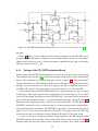
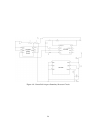
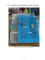
In the controlled airspace boundary detector circuit, the input, power measuring and output
stages are connected together as shown in figure 4.6. The RF output of the input filter is
connected to the RF input (J1) of the LTC5507 demo board. The output of the LTC demo
board at terminal E2 is connected to the In+ of the AZV393 voltage comparator. The reference voltage to the In- input of the voltage comparator is supplied from the output of the
potential divider formed by R1 and R2. An LED is connected between the ouput pin of the
voltage comparator and ground. Chapter 5 discusses the testing of the system, including the
configuration of the detection threshold.
27
Figure 4.6: Controlled Airspace Boundary Detector Circuit
28
Chapter 5
Results and Analysis
This chapter discusses the testing of the detector circuit and the selection of a detection
threshold based on those tests.
5.1
Overview
The detector circuit shown in figure 4.6 needs to be configured so that it will only light the
warning LED when a real signal is detected. This configuration is accomplished in two
stages. First, the output of the combined input and power metering stages must be measured
while a signal is being input at different frequencies. The results of these tests must be used
to decide on an appropriate reference voltage for the voltage comparator of the output stage.
5.2
Testing the Input and Power Measuring Stages
To test the input and power measuring stages, a signal generator was connected to the RF
input of the filter, instead of the antenna shown in figure 4.6. The output from the LTC5507
demo board was directly measured using an oscilloscope. The signal generator was set
to different frequencies and the output of the LTC5507 demo board was recorded at each
frequency. The frequencies ranged from below the passband of the A11535 filter to above
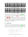
the passband [51]. Table 5.1 shows the results of these tests. The output values for 108MHz
and 118MHz (the edges of the VOR band) are 300mV and 440mV, respectively. It was
decided that the reference voltage supplied to the voltage comparator should therefore be
greater than 440mV. A value of 445mV was chosen to ensure that only signals from the
VOR frequency range would trigger the detector.
5.3
Configuring the Detection Threshold
Choosing a detection threshold required selecting values for resistors R1 and R2 in the potential divider in figure 4.6. A 10kΩ resistor was chosen for R1. The value of R2 was calculated
29
Input Frequency
MHz
100
103
106
108
109
112
115
118
121
124
127
130
Output Voltage
mV
290
290
290
300
310
380
460
440
400
380
360
340
Table 5.1: Input and Power Measuring stage test results at 0dBm
using equation 2.5. The power supply voltage (5V), is VIN . VOUT is 445mV for the reasons discussed in the previous section. The value calculated for R2 was 976Ω, therefore a
1kΩ resistor was used as R2. The output of the potential divider was then connected as the
reference voltage to the AZV393 voltage comparator.
Testing of the circuit with this combination of resistors revealed that it falsely detected
frequencies as high as 125MHz. The value of R2 was increased in 50Ω steps, until the
circuit only responded to frequencies within the VOR range. The final value of R2 was
1.2kΩ, which corresponds to a potential divider output/reference voltage of 536mV.
5.4
Final Testing
The final reference voltage of 536mV is clearly greater than the peak output voltage of
460mV at 115MHz in table 5.1. This inconsistency was investigated, by measuring the
output voltage of the power measuring stage while it was connected to the voltage comparator. The frequency was swept from 100MHz to 130MHz in increments of 3MHz and the
output measured at each step. It was observed during these tests that the output of the circuit
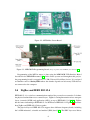
fluctuated, depending on the relative positions of the various co-axial cables and the oscilloscope probes. It was theorized based on this behaviour that interference existed between
various parts of the circuit.
Two possible causes for the interference were identified: (a) that the input cable from the
signal generator and the output cable from the filter were interfering with each other, and (b)
that the use of two ground rails (joined with a length of wire) on the breadboard was acting
as an antenna. Figure B.2 shows a picture of the breadboard at the conclusion of the project,
with the ground rails labeled. Due to the time constraints of the project, further testing to
find and eliminate the source of the interference was not possible.
30
Chapter 6
Evaluation and Future Work
This chapter evaluates the Controlled Airspace Boundary Detection project with respect to
the goals outlined in section 1.2. It also outlines some possible future work which would
improve and extend the detector.
6.1
Evaluation
The primary goal of this project was to produce a detector capable of providing a pilot with
adequate warning of controlled airspace ahead. With respect to this goal, the final circuit is
reasonably successful. It can detect frequencies in the VOR frequency band and display a
warning in the form of a lighted LED.
There are also some issues with the final circuit, including:
• Self interference
• Overly restricted bandwidth
• Unknown detection range and limited sensitivity.
The problem of self interference, as outlined in the final section of chapter 5, is the most
serious. This self interference could be reduced in a number of ways, firstly, a replacement
for the LTC5507 RF power meter, suitable for use on a breadboard, could be found. This
would eliminate the co-axial cable from the input stage components to the LTC5507 demo
board. Secondly, the components could be rearranged on the breadboard so that only one
ground rail would be utilised. Finally, the rearrangement of the components should be done
in a way that minimised the length of all wires on the breadboard. This would help to reduce
the potential of each wire to act as an unwanted antenna.
The bandwidth restriction is caused by the A11535 filter. which supresses all VOR frequencies outside it’s 112.5MHz to 117.5MHz passband. This problem could be solved by
locating and installing, a filter with a 10MHz bandwidth centered at 113MHz, the exact
center of the VOR band.
31
The detection range of the circuit, can only be determined by experiment. The output
power of a VOR transmitter would need to be measured. Then the RF power at the controlled airspace boundary would have to be either (a) measured, or (b) calculated from the
transmitter power. The RF power at the desired range could be used in the configuration
phase (described in chapter 5) to decide on a suitable detection threshold.
The limited sensitivity of the circuit, is partly caused (i) by the LTC5507 chip having a
lower power detection threshold of -34dBm, and (ii) by losses in the A11535 filter, which
reduce the signal power reaching the power measuring stage.
6.2
Future Work
In light of the recent commercial release of the Aware GPS system (a GPS-based navigation system that uses a built-in map to provide warnings of controlled airspace [57]), one
possible avenue of future work is to enhance our system to recognise and handle real-time
updates to controlled airspace. For example, the Controlled Airspace Boundary Detector
could be redesigned to receive notifications of updated airspace boundaries from an airport.
It could then incorporate these changes into the Aware system’s on-board map. Such a realtime updating of the controlled airspace would prevent pilots accidentally infringing newly
controlled airspace.
32
Appendix A
Code Listings
A.1
Blink Demonstration Application
A.1.1
Blink Configuration Code
configuration BlinkAppC
{
}
implementation
{
components MainC, BlinkC, LedsC;
components new TimerMilliC() as Timer0;
BlinkC -> MainC.Boot;
BlinkC.Timer0 -> Timer0;
BlinkC.Leds -> LedsC;
}
A.1.2
Blink Module Code
#include "Timer.h"
module BlinkC @safe()
{
uses interface Timer<TMilli> as Timer0;
uses interface Leds;
uses interface Boot;
}
implementation
{
33
event void Boot.booted()
{
call Timer0.startPeriodic( 250 );
}
event void Timer0.fired()
{
dbg("BlinkC","Timer 0 fired @ %s.\n", sim_time_string());
call Leds.led0Toggle();
}
}
A.2
ReadRSSI Version One Code
A.2.1
ReadRSSI Configuration Code
#include "printf.h"
configuration RssiAppC
{
}
implementation
{
components MainC, RssiC, LedsC;
components new TimerMilliC() as Timer0;
components CC2420ControlC;
components HplCC2420InterruptsC;
// components new CC2420SpiC();
// components new AMReceiverC(6) as Receiver;
RssiC -> MainC.Boot;
RssiC.Timer0 -> Timer0;
RssiC.Leds -> LedsC;
RssiC.Read -> CC2420ControlC.ReadRssi;
RssiC.Resource -> CC2420ControlC.Resource;
RssiC.Config -> CC2420ControlC.CC2420Config;
RssiC.Power -> CC2420ControlC.CC2420Power;
RssiC.Sfd -> HplCC2420InterruptsC.CaptureSFD;
RssiC.Cca -> HplCC2420InterruptsC.InterruptCCA;
RssiC.Fifo -> HplCC2420InterruptsC.InterruptFIFOP;
34
//
//
//
}
RssiC.ReadRxFiFo -> CC2420SpiC.RXFIFO;
RssiC.ClearRxFifo -> CC2420SpiC.SFLUSHRX;
RssiC.Receive -> Receiver;
A.2.2
ReadRSSI Module Code
#include "Timer.h"
#include "printf.h"
module RssiC @safe()
{
uses interface Timer<TMilli> as Timer0;
uses interface Leds;
uses interface Boot;
uses interface Read<uint16_t>;
uses interface CC2420Config as Config;
uses interface CC2420Power as Power;
uses interface Resource;
uses interface GpioCapture as Sfd;
uses interface GpioInterrupt as Cca;
uses interface GpioInterrupt as Fifo;
// uses interface Receive;
// uses interface CC2420Fifo as ReadRxFiFo;
// uses interface CC2420Strobe as ClearRxFifo;
}
implementation
{
enum {
STATE_OFF = 1,
STATE_STARTING = 2,
STATE_STARTED = 3
};
// uint16_t i = 0;
uint8_t ctr = 0;
uint8_t dummy_data = 0;
uint8_t state = STATE_OFF;
event void Boot.booted()
{
35
//
//Start the timer
call Timer0.startPeriodic( 500 );
call Timer0.startOneShot(1000);
//Switch on the radio chip.
call Power.startVReg();
atomic
{
state = STATE_STARTING;
}
}
event void Timer0.fired()
{
ctr++;
printf("%d", ctr);
printfflush();
//Check if the radio has started and read RSSI if it has.
atomic
{
if (state == STATE_STARTED)
{
//call ReadRxFiFo.beginRead(&dummy_data, 1);
//call ClearRxFifo.strobe();
//call ClearRxFifo.strobe();
call Read.read();
}
}
call Leds.set(ctr);
}
// Events of the CC2420ControC module
async event void Power.startVRegDone() {
//printf("startVregDone");
//printfflush();
call Resource.request();
}
36
event void Resource.granted()
{
printf("resource granted event, starting oscillator");
printfflush();
call Power.startOscillator();
}
async event void Power.startOscillatorDone()
{
//printf("start osc done");
//printfflush();
call Fifo.enableFallingEdge();
call Sfd.captureRisingEdge();
call Power.rxOn();
call Resource.release();
//
call Config.setAddressRecognition(FALSE, FALSE);
//Change state to started
atomic
{
state = STATE_STARTED;
}
}
event void Config.syncDone(error_t error)
{
printf("sync done");
printfflush();
}
event void Read.readDone(error_t result, uint16_t val)
{
if ( result == SUCCESS )
{
printf("\t\t%d\n", val);
}
else
{
printf("failed to read rssi\n");
37
}
printfflush();
}
// Events from HplCC2420InterruptsC
async event void Sfd.captured(uint16_t time)
{
}
async event void Cca.fired()
{
}
async event void Fifo.fired()
{
}
//Events from the RXFIFO
// async event void ReadRxFiFo.readDone(uint8_t *data,
//
uint8_t length, error_t error)
// {
// }
//
//
//
//
async event void ReadRxFiFo.writeDone(uint8_t *data,
uint8_t length, error_t error)
{
}
//Receiver events
// event message_t* Receive.receive(message_t* msg,
//
void* payload, uint8_t len) {
//
printf("hello \n");
//
printfflush();
//
return msg;
// }
}
38
A.3
ReadRSSI Version Two Code
A.3.1
ReadRSSI Configuration Code V2
#include "printf.h"
configuration RssiAppC
{
}
implementation
{
components MainC, RssiC, LedsC;
components new TimerMilliC() as Timer0;
components CC2420ControlC;
components ActiveMessageC;
RssiC -> MainC.Boot;
RssiC.Timer0 -> Timer0;
RssiC.Leds -> LedsC;
RssiC.Read -> CC2420ControlC.ReadRssi;
RssiC.AMControl -> ActiveMessageC;
RssiC.Config -> CC2420ControlC.CC2420Config;
}
A.3.2
ReadRSSI Module Code V2
#include "Timer.h"
#include "printf.h"
module RssiC @safe()
{
uses interface Timer<TMilli> as Timer0;
uses interface Leds;
uses interface Boot;
uses interface Read<uint16_t>;
uses interface CC2420Config as Config;
uses interface SplitControl as AMControl;
}
implementation
{
enum {
39
STATE_OFF = 1,
STATE_STARTING = 2,
STATE_STARTED = 3
};
uint8_t ctr = 0;
uint8_t dummy_data = 0;
uint8_t state = STATE_OFF;
event void Boot.booted()
{
//Switch on the radio chip.
call AMControl.start();
}
event void AMControl.startDone(error_t err)
{
if (err == SUCCESS)
{
atomic
{
state = STATE_STARTED;
}
//Start the timer
call Timer0.startPeriodic( 50 );
}
else
{
call AMControl.start();
}
}
event void Timer0.fired()
{
ctr++;
printf("%d", ctr);
printfflush();
//Check if the radio has started and read RSSI if it has.
atomic
40
{
if (state == STATE_STARTED)
{
call Read.read();
}
}
call Leds.set(ctr);
}
event void Read.readDone(error_t result, uint16_t val)
{
if ( result == SUCCESS )
{
printf("\t\t%d\n", val);
}
else
{
printf("failed to read rssi\n");
}
printfflush();
}
event void AMControl.stopDone(error_t err)
{
}
event void Config.syncDone(error_t error){
}
}
A.4
Task-based ReadRSSI module code
#include "Timer.h"
#include "printf.h"
module
{
uses
uses
uses
RssiC @safe()
interface Leds;
interface Boot;
interface Read<uint16_t>;
41
uses interface CC2420Config as Config;
uses interface SplitControl as AMControl;
}
implementation
{
//Global variables
enum {
STATE_OFF = 1,
STATE_STARTING = 2,
STATE_STARTED = 3
};
uint8_t ctr = 0;
uint8_t state = STATE_OFF;
//Task declaration
task void readRssiTask();
event void Boot.booted()
{
//Switch on the radio chip.
call AMControl.start();
state = STATE_STARTING;
}
event void AMControl.startDone(error_t err)
{
if (err == SUCCESS)
{
state = STATE_STARTED;
//Radio is started so post the read rssi task.
post readRssiTask();
}
else
{
call AMControl.start();
}
}
42
task void readRssiTask()
{
ctr++;
//Check if the radio has started and post
//readRSSITask if it has.
if (state == STATE_STARTED)
{
if (call Read.read() != SUCCESS)
{
post readRssiTask();
}
}
}
event void Read.readDone(error_t result, uint16_t val)
{
if ( result == SUCCESS )
{
if (val > 80)
{
printf("%d\n", val);
call Leds.set(ctr);
}
}
else
{
printf("failed to read rssi\n");
}
printfflush();
post readRssiTask();
}
event void AMControl.stopDone(error_t err){
}
event void Config.syncDone(error_t error){
}
}
43
Appendix B
Miscellaneous
B.1
Conversion chart from dBm to W
dBm
mW
15
32
5
3.2
0
1
-10
0.1
-85
3.2 × 10⁻⁹
-95
3.2 × 10⁻¹⁰
-100
1 × 10⁻¹⁰
Table B.1: dBm to mW conversion chart
44
B.2
TinyOS radio stack implementation for cc2420
Figure B.1: TinyOS radio stack for cc2420 (Image reproduced from CC2420ActiveMessageC documentation [58])
45
B.3
Controlled Airspace Boundary Detector Prototype
Figure B.2: Picture of the prototype on a breadboard
46
B.4
Listing of Lab Equipment
The following instruments were used in the development and testing of the dedicated hardware described in chapter 4.
• Thurlby Thandar Instruments (TTI) TG215 2MHz Function Generator.
• TTI EL302D Dual Power Supply
• Kenwood 40MHz Oscilloscope CS-4135
• Tektronix TDS3034 - 4 channel color digital phosphor oscilloscope 300Mhz
• Marconi Instruments 80kHz - 1040Mhz signal generator. Model 2019
• Hewlett Packard spectrum analyser 1kHz - 22GHz. Model 8562A
• Prototyping board (breadboard)
47
Bibliography
[1] (2010, Aug.) Annual Aviation Safety Performance Review 2009. [Online]. Available:
http://www.iaa.ie/library download.jsp?libraryID=756
[2] (2010) Occurence reporting. [Online]. Available:
139&n=148
http://www.iaa.ie/index.jsp?p=
[3] (2010, Aug.) Airspace Infringements Background Statistics. [Online]. Available:
http://www.flyontrack.co.uk/scripts/MIAB/MIAB ShowAsset.asp?a=-2147483622
[4] (2010, Aug.) Annual Report 2009. [Online].
dublinairportauthority.com/AR 2009 English.pdf
Available:
http://www.
[5] (2010, Aug.) Rules of the air, annex 2 to the convention on international civil
aviation. Annex2.pdf. [Online]. Available: http://www2.tech.purdue.edu/at/courses/
at300/Documents/Annex2.pdf
[6] (2010) The ICAO website. [Online]. Available: http://www.icao.int/
[7] (2010, Aug.) ENR 1.4 ATS Airspace Classifications. EI ENR 1 4 en.pdf. [Online].
Available: http://www.iaa.ie/safe reg/iaip/Published%20Files/AIP%20Files/ENR/EI
ENR 1 4 en.pdf
[8] (2010) How atc works? [Online]. Available: http://www.iaa.ie/index.jsp?n=248&p=
153
[9] (2010) Air traffic services & technology. [Online]. Available: http://www.iaa.ie/index.
jsp?p=153&n=247
[10] (2010, Aug.) Comreg radio frequency plan for ireland. ComReg0477R 39076827.pdf.
[Online]. Available: http://www.comreg.ie/ fileupload/publications/ComReg0477R
39076827.pdf
[11] (2010) Air traffic services & technology. [Online]. Available: http://www.iaa.ie/index.
jsp?p=155&n=255
[12] (2010) Surveillance / radar. [Online]. Available:
155&n=257
48
http://www.iaa.ie/index.jsp?p=
[13] (2010, Aug.) Mode s technical overview. [Online]. Available: http://www.eurocontrol.
int/msa/public/standard page/modes tech overview.html
[14] (2010, Aug.) Mode s technology. [Online]. Available: http://mit.edu/6.933/www/
Fall2000/mode-s/technology.html
[15] (2010) Navigation. [Online]. Available: http://www.iaa.ie/index.jsp?p=155&n=256
[16] (2010, Aug.) Operational notes on vhf omni range VOR. [Online]. Available:
http://www.casa.gov.au/wcmswr/ assets/main/pilots/download/vor.pdf
[17] (2010, Aug.) 2001 federal radio navigation systems. FRS2001.pdf. [Online]. Available:
http://www.navcen.uscg.gov/pdf/frp/frp2001/frs2001.pdf
[18] (2010, Aug.) AIP Ireland, EIDW AD 2 - 1. [Online]. Available: http://www.iaa.ie/
safe reg/iaip/Published%20Files/AIP%20Files/AD/EI AD 2 EIDW en.pdf
[19] (2010) Crossbow website. [Online]. Available: http://www.xbow.com/
[20] (2010, Aug.) MICAz 2.4ghz wireless module. [Online]. Available: http://memsic.com/
products/wireless-sensor-networks/wireless-modules.html
[21] (2010,
Aug.)
MPR-MIB
Users
Manual.
Revision
A,
June
2007.
MEMSIC.
PN:
7430-0021-08.
[Online].
Available: http://memsic.com/support/documentation/wireless-sensor-networks/category/
6-user-manuals.html?download=61%3Ampr-mib-wireless-module-user-s-manual
[22] (2010, Aug.) Chipcon cc2420 2.4 GHz IEEE 802.15.4 ZigBee-ready RF Transceiver.
Rev B, 20 Mar 2007. Texas Instruments. SWRS041B. [Online]. Available:
http://www.ti.com/lit/gpn/cc2420
[23] W. Su and M. Alzaghal, “Channel propagation characteristics of wireless micaz sensor
nodes,” Ad Hoc Netw., vol. 7, no. 6, pp. 1183–1193, 2009.
[24] (2010) Part 15.4: Wireless Medium Access Control(MAC) and Physical Layer(PHY)
Specifications for Low-Rate Wireless Personal Area Networks (WPANs). [Online].
Available: http://standards.ieee.org/getieee802/download/802.15.4-2006.pdf
[25] K. Srinivasan and P. Levis, “Rssi is under appreciated,” in In Proceedings of the Third
Workshop on Embedded Networked Sensors (EmNets), 2006.
[26] (2010, Mar.) ATmega128 AVR 8-bit Microcontroller with 128K Bytes InSystem Programmable Flash. Rev. 2467SAVR07/09. Atmel. [Online]. Available:
http://www.atmel.com/dyn/resources/prod documents/doc2467.pdf
[27] (2010) Sensor boards. MEMSIC. [Online]. Available: http://memsic.com/products/
wireless-sensor-networks/sensor-boards.html
49
[28] P. Baronti, P. Pillai, V. Chook, S. Chessa, A. Gotta, and Y. Hu, “Wireless sensor networks: A survey on the state of the art and the 802.15. 4 and ZigBee standards,” Computer Communications, vol. 30, no. 7, pp. 1655–1695, 2007.
[29] Z. Alliance, “Zigbee-2006 specification,” ZigBee Alliance, 2006.
[30] (2010, Aug.) TinyOS Community Forum. [Online]. Available: http://www.tinyos.net/
[31] P. Levis and D. Gay, TinyOS Programming, 1st ed. Cambridge University Press, 2009.
[32] (2010, Mar.) Getting Started with TinyOS. [Online]. Available: http://docs.tinyos.net/
index.php/Getting Started with TinyOS
[33] (2010, Aug.) Modules and the TinyOS Execution Model. [Online]. Available:
http://docs.tinyos.net/index.php/Modules and the TinyOS Execution Model
[34] (2010, Aug.) United States Updates Global Positioning System Technology. [Online]. Available: http://www.america.gov/st/washfile-english/2006/February/
20060203125928lcnirellep0.5061609.html
[35] (2010, Aug.) Global Positioning System. [Online]. Available: http://www.gps.gov/
systems/gps/index.html
[36] (2010, Aug.) The Global Positioning System. [Online]. Available: http://www.
colorado.edu/geography/gcraft/notes/gps/gps f.html
[37] M. Mansfield and C. O’Sullivan, Understanding Physics.
John Wiley & Sons, 1999.
[38] S. R. Saunders, Antennas and Propagation for Wireless Communication Systems. John
Wiley & Sons, 2004.
[39] (2010,
Aug.)
MTS/MDA
Sensor
Board
Users
Manual.
Revision A, June 2007. MEMSIC. PN: 7430-0020-05. [Online]. Available: http://memsic.com/support/documentation/wireless-sensor-networks/category/
6-user-manuals.html?download=62%3Amts-mda-sensor-board-user-s-manual
[40] (2010, Aug.) TinyOS Tutorials. [Online]. Available: http://docs.tinyos.net/index.php/
TinyOS Tutorials
[41] (2010, Aug.) TEP’s. [Online]. Available: http://docs.tinyos.net/index.php/TEPs
[42] (2010, Aug.) RSSI demo. [Online]. Available:
Rssi Demo
http://docs.tinyos.net/index.php/
[43] (2010, Aug.) The TinyOS printf Library. [Online]. Available: http://docs.tinyos.net/
index.php/The TinyOS printf Library
50
R
[44] (2010, Aug.) LEA-4A ANTARIS
4 GPS Modules. Dec 2006. GPS.G4-MS4-061431. [Online]. Available: http://www.u-blox.com/images/downloads/Product Docs/
LEA-4x Data Sheet%28GPS.G4-MS4-06143%29.pdf
[45] (2010, Aug.) MTS420. [Online]. Available: http://docs.tinyos.net/index.php/MTS400
[46] (2010, Aug.) SourceForge.net Repository - [TinyOS] Index of /tinyos-2.xcontrib/rincon. [Online]. Available: http://tinyos.cvs.sourceforge.net/viewvc/tinyos/
tinyos-2.x-contrib/rincon/
[47] (2010, Aug.) Leadtek. [Online]. Available:
http://www.leadtek.com.tw/
downloads/?lang=eng&filepath=/gps/9546/&filename=9546Manual%5FV1%2E12%
5F20030806%2Epdf
[48] (2010, Aug.) National Marine Electronics Association. [Online]. Available: http:
//www.nmea.org/content/nmea standards/nmea 083 v 400.asp
[49] R. Silva, J. S. Silva, C. Geyer, V. Leithard, and F. Boavida, “Use of gps and 6lowpan in
mobile multi-sink wireless sensor networks - issues and feasibility,” in 8th International
Information and telecommunication Technologies Symposium (I2TS), Dec. 2009, pp.
154–160, ISBN 978-85-8.
[50] (2010, Aug.) MS5534C Altimeter/Barometer Module. [Online]. Available: http://www.
intersema.ch/index.php?option=com rubberdoc&view=doc&id=35&format=raw
[51] (2010, Aug.) 115MHz Bandpass Filter 4.92MHz Bandwidth. [Online]. Available:
http://www.amtsaw.com/brochure/saw/A11535.pdf
[52] E. Benes, M. Groschl, F. Seifert, and A. Pohl, “Comparison between BAW and SAW
sensor principles,” in Frequency Control Symposium., Proceedings of the 1997 IEEE
International, may. 1997, pp. 5 –20.
[53] (2010, Aug.) LTC5507 - 100kHz to 1GHz RF Power Detector. [Online]. Available:
http://cds.linear.com/docs/Datasheet/5507f.pdf
[54] (2010, Aug.) DC489 - LTC5507 Evaluation Kit. [Online]. Available:
//cds.linear.com/docs/Reference%20Design/dc489A.pdf
[55] M. J. Cooke, Semiconductor devices.
USA, 1990.
http:
Prentice-Hall, Inc. Upper Saddle River, NJ,
[56] (2010, Aug.) Dual General Purpose Low Voltage Comparator, AZV393. [Online].
Available: http://www.bcdsemi.com/upload/datasheet/AZV393%20D1.3%20091117.
pdf
[57] (2010, Sep.) The Aware Airspace Alerting Tool. [Online]. Available:
//www.airspaceaware.com/aboutaware/
51
http:
[58] (2010, Aug.) Interfaces and Components. [Online]. Available: http://www.tinyos.net/
tinyos-2.x/doc/nesdoc/micaz/index.html
52