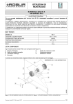
1
AK 2007-06/1
Universität Mannheim
Lehrstuhl Informatik V
Insitut für Technische Informatik
User Manual
Document Version:
Document ID:
Document Date:
Document Status:
1.0
AK 2007-06/01
1899-12-30
Draft
Abstract
User manual for the re-configurable accelerator MPRACE-2.
Institutes and Authors:
Mannheim University: A. Kugel
0
00
page 1
0
0
Version/Issue: 10/6
Table 1 Document Change Record
Title:
MPRACE-2 User Manual
ID:
AK 2007-06/01
Version
Issue
Date
Comment
1
1
2007-06-19
Birth
1
2
2007-09-07
Updates
1
4
2007-11-06
More updates
1
5
2008-03-28
Clock usage
1
6
2008-04-09
Pin infos and K-characters
1
7
2010-09-13
Test pin info added
page 2
0
ATLAS TDAQ 0
Version/Issue: 10/6
Contents
1INTRODUCTION.........................................................................................5
1.1GLOSSARY, ACRONYMS AND ABBREVIATIONS...................................................5
1.2REFERENCES....................................................................................................5
2BOARD DESCRIPTION................................................................................5
3CONFIGURATION.......................................................................................7
3.1JTAG CONFIGURATION.....................................................................................7
3.1.1CPLD configuration....................................................................................................7
3.1.2FPGA configuration....................................................................................................7
4POWER-ON CONFIGURATION....................................................................8
5PARALLEL CONFIGURATION....................................................................10
6LED BLOCK...............................................................................................11
7CLOCK RESSOURCES................................................................................11
8CONTROL CPLD........................................................................................12
8.1SWITCHES......................................................................................................12
9BRIDGE FPGA...........................................................................................12
9.1FPGA..............................................................................................................12
9.2SDRAM...........................................................................................................12
9.3ETHERNET......................................................................................................12
9.4SERIAL PORT..................................................................................................12
9.5CPLD INTERFACE............................................................................................13
9.6FLASH INTERFACE..........................................................................................13
9.7PROGRAMMABLE CLOCKS................................................................................13
9.8PCIE / PCI-X...................................................................................................13
10MAIN FPGA............................................................................................14
10.1SRAM BANKS................................................................................................14
10.2DRAM BANK..................................................................................................14
10.3MEZZANINE INTERFACE................................................................................14
10.3.1Interface signals....................................................................................................14
10.3.2Power supply........................................................................................................14
10.4BOARD-TO-BOARD INTERFACE......................................................................14
11REFERENCE DESIGNS............................................................................15
11.1DESIGN RULES..............................................................................................15
11.2CONFIGURATION..........................................................................................15
11.2.1CfgTest ................................................................................................................15
12APPENDIX..............................................................................................16
12.1MGT NUMBERING SCHEME............................................................................16
page 3
0
0
Version/Issue: 10/6
12.2BRIDGE-MAIN MGT INTERCONNECT..............................................................16
12.3MGT POWERING SCHEME..............................................................................17
12.4MGT REFERENCE CLOCK 125 MHZ.................................................................17
12.5MGT LINE RATE SELECTION..........................................................................18
12.6MGT K-CHARACTERS.....................................................................................19
12.7LOGIC CLOCKING SCHEME............................................................................20
12.7.1Clocking overview..................................................................................................20
12.7.2Location of Clock, Reset and Test pins....................................................................20
12.7.3Test headers.........................................................................................................21
12.8ASSEMBLY DRAWINGS..................................................................................22
12.8.1Top......................................................................................................................22
12.8.2Bottom.................................................................................................................22
12.8.3Test-points............................................................................................................23
page 4
0
ATLAS TDAQ 0
Version/Issue: 10/6
1 Introduction
Brief introductory text.
1.1 Glossary, acronyms and abbreviations
Something else to be defined
And here is the description for something else
1.2 References
[1]
[2]
[3]
[4]
[5]
[6]
XILINX Virtex-4 datatsheet, http://direct.xilinx.com/bvdocs/publications/ds302.pdf
XILINX Virtex-4 user guide, http://direct.xilinx.com/bvdocs/userguides/ug070.pdf
XILINX configuration guide: http://direct.xilinx.com/bvdocs/userguides/ug071.pdf
XILINX coolrunner datasheet: http://direct.xilinx.com/bvdocs/publications/ds090.pdf
XILINX coolruner userguide: http://direct.xilinx.com/bvdocs/publications/ds094.pdf
2 Board description
Fehler: Referenz nicht gefunden shows the block diagram of MPRACE-2. A small Virtex4FX FPGA 1.2, 1.2 implements the bridge to PCIe or PCI-X host bus.
Figure 1: Block diagram
page 5
0
0
Version/Issue: 10/6
It is equipped with 16MB of SDRAM, a GbE interface, a serial port and connects to the
control CPLD 1.21.2. Via the CPLD the FLASH memory can be accessed, which stores
configuration bitstreams and potentially boot software for the embedded processor.
The main FPGA connects via 4 serial links and a parallel 32 bit interface to the bridge FPGA.
The parallel interface is mainly intended for configuration purposes (SelectMAP8 or
SelectMAP32), but may be used otherwise as well. The main FPGA is equipped with 2 banks
of SRAM and 1 bank of DRAM, all of DDR-2 type. A set of high-speed connectors enable
expansion via mezzanine boards. In addition, two (e.g. daisy-chain style) board-to-board
connections can be established via serial links.
Main FPGA
PwrReg PwrReg PwrReg
PwrReg PwrReg PwrReg
Mezzanine area
SRAM
SRAM
SRAM
SRAM
Bridge
FPGA
GbE
PHY
PWR
RJ45
CPLD
DDR2-Module
FLASH
Figure 1: Board sketch
A sketch of the final board is shown in Figure 1 and a picture of the first version is shown in
Fehler: Referenz nicht gefunden.
Assembly drawings (version 2) are displayed in sections and .
LED
CPLD JTAG
block
FPGA JTAG
Figure 3: MPRACE-2 (version 1)
page 6
0
ATLAS TDAQ 0
Version/Issue: 10/6
3 Configuration
3.1 JTAG configuration
3.1.1 CPLD configuration
Configuration of the CPLD (XC2C256) is done via JTAG, using the connector at the upper
side of the board (close to main FPGA).
3.1.2 FPGA configuration
JTAG configuration of the two FPGAs is done via the lower connector, close to the PCIe/PCIX connector. The FPGAs form a chain – defined by logic in the CPLD – with the main FPGA
next to the TDI pin and the bridge FPGA next to the TDO pin (=> main is first device/LEFT,
bridge is second device/RIGHT in JTAG chain), see Figure 4.
The JTAG chain is defined by the CPLD and can be modified to include other JTAG-capable
resources on the board.
Figure 4: FPGA JTAG Chain
page 7
0
0
Version/Issue: 10/6
4 Power-on configuration
The 8MB FLASH memory provides space for 2 sets of configuration bitstreams and for
PowerPC software. The memory regions are defined by the CPLD. For the MPRACE-2
prototypes which have an XC4VFX60 device as bridge care has to be taken, that the combined
size of the bridge and main FPGA bitstreams does not exceed 3MB. This can normally be
achieved using bitstream compression, but cannot be guaranteed for all designs. For the
moment, the configuration set is selected using one of the DIP switches. However, an
automatic setting using the PCI-power-available signal can also be implemented, by
modification of the CPLD code.
Figure 2: Prepare PROM
The configuration bitstreams are loaded by the CPLD in slave-serial mode into the chain of
the two FPGAs. The first device is the bridge FPGA.
The top-most 2MB of the FLASH can be used for boot-code for the PowerPC in the bridge
FPGA.
The FLASH file has to be prepared from two bitfiles, with the BRIDGE content located at the
beginning (lower address). Impact can be used to generate the content in HEX format (see
below). Make sure that the proper bitstream region is selected via the switch.
Click “finish” on the third screen.
page 8
0
ATLAS TDAQ 0
Version/Issue: 10/6
Figure 3: Select device
Figure 4: Start adding data
page 9
0
0
Version/Issue: 10/6
Now add the bitfile for the BRIDGE, followed by the bitstream for the MAIN FPGA. The bitstreams
should be generated with CCLK and drive DONE options (DONE pins are NOT wired-and on
MPRACE-2). There are no data-file parameters (clock OK on that screen).
Figure 5: Prom with data files
Now click “Generate File” in the operations tab. The file will be in HEX format and needs to be
converted by the download utility.
5 Parallel configuration
While the bridge FPGA can only be configured through the CPLD (power-up or JTAG) the
main FPGA can be configured also from a host PC through the bridge FPGA, in one of the
parallel SelectMAP modes SMAP8 or SMAP32. SMAP32 mode requires a special setting in
the UCF file of the FPGA project:
CONFIG CONFIG_MODE=S_SELECTMAP32;
or
CONFIG CONFIG_MODE=S_SELECTMAP32+READBACK;
The latter is required if readback or re-configuration will be used and makes the SMAP32
interface persistent.
Designs compiled without this constraint have to use the SMAP8 mode 1.
1
page 10
To be confirmed
0
ATLAS TDAQ 0
Version/Issue: 10/6
6 LED Block
A number of LEDs are used to display status information: 4 LEDs connect to the CPLD and
two LEDs to each of the FPGAs. The LED are labelled (left to right): D5000, D5001,
Figure 9: LED block
LD6000, LD4001, LD4000. D5000 and 5001 are single LEDs, the others are bi-colour LEDs.
The LEDs are positioned in the upper right area of the board, close to the upper JTAG
connector, a shown in Fehler: Referenz nicht gefunden.
LED
Signal
Usage
D5000
Main LED0
Design dependent
D5001
Main LED1
Design dependent
LD6000-upper (green)
Bridge LED1
Design dependent
LD6000-lower (red)
Bridge LED0
Design dependent
LD4001-upper (green)
CPLD LED3
ON if PCI power (12V) available
LD4001-lower (red)
CPLD LED2
On if power-up configuration in progress
LD4000-upper (green)
CPLD LED1
Reset completed (OFF during reset)
LD4000-lower (red)
CPLD LED0
Power good (normally ON)
Table 2: LED block
7 Clock ressources
A number of fixed and variable frequency oscillators is available on MPRACE-2. All MGT
clocks, with the exception of the PCIe interface, can be derived from the dual-frequency
oscillator U5004, which provides 125MHz (default) 2 or 156.25MHz, selectable via a CPLD
signal. On the MAIN FPGA, the MGT clocks can alternatively be derived from the
programmable clock source U5005 (see section 9.7).
2
According to the 2008 datasheet, an MGT reference clock of 125 MHz is no longer valid. In future
assembly versions the 125MHz will be replaced by 250MHz. See appendix 12.4 on how to modify
MGT cores generated by the XILINX tools to use 125MHz.
page 11
0
0
Version/Issue: 10/6
8 Control CPLD
..\vhdl\cpld\cpld1\latex\refman.pdf
8.1 Switches
All switches are defined by the CPLD. The current layout is as follows:
1
2
3
4
5
6
7
8
Off: Full chain, On: only FPGA
OFF: upper FLASH offset, ON: lower FLASH offset
Off: fan controlled by temperature sensor. On: fan on
Off: auto config after powerup, On: no auto config
Off: pci_reset used to trigger reconfiguration. ON:
don't use pci reset
Directly mapped to CLK_SEL input of U5004 to select
125 (0) or 156,25 MHz (1). U5001 fixed to 0
General purpose bit forwarded to bridge FPGA via
bio_switch
Unused
Default settings are (switch 1 left most one)
ON, ON, ON, OFF, ON, ON, OFF, OFF
9 Bridge FPGA
9.1 FPGA
9.2 SDRAM
9.3 Ethernet
9.4 Serial Port
A small connector (P6000, next to the battery) provides two serial interfaces, one from each
FPGA:
5
3
1
Bridge-RxD
GND
Bridge-TxD
Main-TxD
GND
Main-RxD
6
4
2
The corresponding FPGA pins are:
Main-TxD
: AE21
Main-RxD : AF19
Bridge-TxD : A14
Bridge-RxD : A13
page 12
0
ATLAS TDAQ 0
Version/Issue: 10/6
To connect to the serial port of a PC, the pins must be connected to the following pins of a 9pin sub-D connector:
•
Bridge (MPRACE-2 -> sub-D): 5 – 3, 3 – 5, 1 – 2
•
Main (MPRACE-2 -> sub-D): 6 – 3, 4 – 5, 2 – 2
9.5 CPLD Interface
9.6 FLASH Interface
9.7 Programmable Clocks
Two programmable clock generators ICS8430AYI-61LF are available to provide clock
frequencies in the range of 25 to 250 MHz to the main FPGA. One generator feeds the FPGA
fabric clocking resources, the other one feeds a MGT clock in each of the two columns. The
clock generators are programmed to a default frequency of 125MHz via the RESET signal.
Care must be taken that the control lines from the bridge FPGA are properly initialised to 0.
9.8 PCIe / PCI-X
MPRACE-2 uses the following PCI configuration words (hex):
PCIe Version:
• Vendor ID: 10DC
• Device ID: 0153
• Subsystem vendor ID: 0084
• Subsystem device ID: AC2E
PCI-X Version:
• Vendor ID: 10DC
• Device ID: 0153
• Subsystem vendor ID: 0084
• Subsystem device ID: AC2A
page 13
0
0
Version/Issue: 10/6
10 Main FPGA
Me z z - MGT s
DDR2 S DRAM
Ad d - On Co n n e c t o r
601 K NAB
901 K NAB
BANK 110
BANK 105
Ca b l e 1- MGT s
2 K NAB
7 K NAB
8 K NAB
4 K NAB
21 K NAB
11 K NAB
BANK 103
A GP F
BANK 112
Ca b l e 2 - MGT s
01 K NAB
9 K NAB
3 K NAB
BANK 113
6 K NAB
1 K NAB
5 K NAB
BANK 102
DDR2 S RAM
Au r o r a - MGT s
Figure 6: Main FPGA bank and MGT usage
10.1 SRAM banks
10.2 DRAM bank
10.3 Mezzanine interface
10.3.1 Interface signals
10.3.2 Power supply
10.4 Board-to-board interface
page 14
DDR2 S RAM
0
ATLAS TDAQ 0
Version/Issue: 10/6
11 Reference designs
11.1 Design Rules
11.2 Configuration
11.2.1 CfgTest
CfgTest is available at the CVS repository and provides the following functionality
• Access to CPLD registers
• Access to FLASH memory
• SMAP8 and SMAP32 configuration of MAIN FPGA
• Access to MAIN FPGA register area (dummy RAM) via PCI BAR2
It consists of the following modules:
• BRIDGE FPGA design mprace2/vhdl/bridge/hwtest/cfgTest
• MAIN FPGA design mprace2/vhdl/main/hwtest/clkTest
• Test program mprace2/c/cfgTest
page 15
0
0
Version/Issue: 10/6
12 Appendix
12.1 MGT numbering scheme
MAIN FPGA :Fx60 / FX100
GT11CLK102 = X0Y3
GT11CLK105 = X0Y1
GT11CLK113 = X1Y3
GT11CLK110 = X1Y1
ProgClk
Gt11106A = X0Y1
Gt11106B = X0Y0
Gt11105A = X0Y3
Gt11105B = X0Y2
Gt11103A = X0Y5
Gt11103B = X0Y4
Gt11102A = X0Y7
Gt11102B = X0Y6
Gt11109A = X1Y1
Gt11109B = X1Y0
Gt11110A = X1Y3
Gt11110B = X1Y2
Gt11112A = X1Y5
Gt11112B = X1Y4
Gt11113A = X1Y7
Gt11113B = X1Y6
Mezz
2
3
0
1
2
3
0
1
A
B 106
A
105
B
A
103
B
105
110
109
Main FPGA
XC4VFX60
A
102
B
102
113
102
110
A
B
110 A
B
A
112 B
A
113
B
0
1
2
3
0
1
2
3
Gt11114A = X0Y9
Gt11114B = X0Y8
B2Bup
B2Bdn
CLK125
Bridge FPGA: Fx20 (FX60)
GT11CLK105 = X0Y0 (X0Y1)
GT11CLK102 = X0Y1 (X0Y3)
GT11CLK110 = X1Y0 (X1Y1)
GT11CLK113 = X1Y1 (X1Y3)
Gt11102A = X0Y3 (X0Y7)
Gt11102B = X0Y2 (X0Y6)
Gt11105A = X0Y1 (X0Y3)
Gt11105B = X0Y0 (X0Y2)
Additional MGTs Fx100
Gt11101A = X0Y9
Gt11101B = X0Y8
MGT-Clocking
MGT
0
A
102
1
B
2
A
105
B
3
MGT_Clk
Bridge FPGA
XC4VFX20
A
0
110
B
1
A
113
B
105
PCIexpress
FX20:
Lane0: 110A = X1Y1
Lane1: 110B = X1Y0
Lane2: 113A = X1Y3
Lane3: 113B = X1Y2
CLK: 113 = GT11CLKX1Y1
2
3
PCIe
113
PCIeClk
ProgClk
Gt11113A = X1Y3 (X1Y7)
Gt11113B = X1Y2 (X1Y6)
Gt11110A = X1Y1 (X1Y3)
Gt11110B = X1Y0 (X1Y2)
FX60:
Lane0: 110A = X1Y3
Lane1: 110B = X1Y2
Lane2: 113A = X1Y7
Lane3: 113B = X1Y6
12.2 BRIDGE-MAIN MGT Interconnect
MPRACE2Aurora link
Lane 0
Lane 1
Lane 2
Lane 3
MGTCLK
page 16
Bridge
MGT102A
MGT102B
MGT105A
MGT105B
GT11CLK102
FX20
X0Y3
X0Y2
X0Y1
X0Y0
X0Y1
FX60
X0Y7
X0Y6
X0Y3
X0Y2
X0Y3
Pin (p/n)
F26/G26
Main
MGT102A
MGT102B
MGT103A
MGT103B
GT11CLK102
FX60
X0Y7
X0Y6
X0Y5
X0Y4
X0Y3
Pins (p/n)
M34/N34
0
ATLAS TDAQ 0
Version/Issue: 10/6
12.3 MGT powering scheme
3 regulator MGT supply
106
109
105
Main
unused:
106,109
101,114
110
103
112
113
102
101
102
114
103
105
Bridge
unused:
103,112
113
112
110
Bridge 102, 105, 110, 112, 113 connected to VMGTC1.2
Bridge 103, Main 101, 110, 112, 113, 114 connected to VMGTB1.2
Main 102, 103, 105, 106, 109 connected to VMGTA1.2
12.4 MGT reference clock 125 MHz
The latest (2008) XILINX datasheets prohibit the use of a 125 MHz reference clock for data
rates of 2.5 Gbit/s and higher. When CoreGenerator is used to generate such cores, the user
should select the 156,25MHz reference clock. If this is not viable, a 250MHz reference clock
should be selected instead and the generated source files be modified accordingly. The
following list shows the different settings:
1) 250 MHz case
• MGT attributes in instantiation code (VHDL):
RXPLLNDIVSEL => 10,
TXPLLNDIVSEL => 10,
page 17
0
0
Version/Issue: 10/6
•
MGT attributes in UCF constraints (alternative to VHDL):
INST mgt_instance RXPLLNDIVSEL = 10;
INST mgt_instance TXPLLNDIVSEL = 10;
• UCF timing constraints:
NET ref_clk1_left_i PERIOD = 4.0 ns;
2) 125 MHz case
• MGT instantiation code, generic map:
RXPLLNDIVSEL => 20,
TXPLLNDIVSEL => 20,
• MGT attributes in UCF constraints (alternative to VHDL):
INST mgt_instance RXPLLNDIVSEL = 20;
INST mgt_instance TXPLLNDIVSEL = 20;
• UCF constraints:
NET ref_clk1_left_i PERIOD = 8.0 ns;
All tests done so far show proper operation with a 125MHz reference clock as well.
12.5 MGT Line rate selection
The MGT line rate can be selectied to 2.5 Gbit/s or 5.0 Gbit/s via the parameters
TXOUTDIV2SEL/RXOUTDIV2SEL in the VHDL/UCF file. Choose a value of 2 for 2.5
Gbit/s and 1 for 5.0 Gbit/s.
Choose the proper settings for the reference clock as described above.
page 18
0
ATLAS TDAQ 0
Version/Issue: 10/6
12.6 MGT K-characters
Note: Bit positions of 10-bit values are reversed wrt CoreGen.
Normally, one of the K-characters is used for comma-alignement. Two more (K28.1 and K28.7) also
trigger the comma alignement circuitry of the MGT. The others are freely usable. If no protocol is
used, the following map is suggested:
Name
Value
Purpose
K28.5
0xBC
Comma alignement and idle character
K28.0
0x1C
SOP (start of packet)
K28.6
0xDC
EOP (end of packet)
K23.7
0xF7
NACK (transmission error indicator)
K27.7
0xFB
XOFF
K29.7
0xFD
XON
page 19
0
0
Version/Issue: 10/6
12.7 Logic clocking scheme
12.7.1 Clocking overview
Logic-Clocking
2
Mezz.
Main-FPGA
Program.
200MHz
125MHz
/156MHz
ICS
85411
Bridge-FPGA
25MHz
74LVC
125
CPLD
PHY
12.7.2 Location of Clock, Reset and Test pins
FPGA
Signal
Pin location P
Pin location N
MAIN
200MHz ref clock
H17
J17
MAIN
125MHz design clock
K19
J19
MAIN
25MHz clock
J14
NA
MAIN
Programmable clock
K18
K17
MAIN
Mezzanine clock 1
AD21
AD20
MAIN
Mezzanine clock 2
AF16
AE16
MAIN
MGT Clock fixed , loc 102
M34
N34
MAIN
MGT Clock fixed, loc 113
AP3
AP4
MAIN
MGT Clock prog. , loc 105
AP29
AP28
MAIN
MGT Clock prog., loc 110
J1
K1
MAIN
Reset from CPLD
H19
NA
MAIN
Test 0
T26
NA
MAIN
Test 1
R26
NA
MAIN
Test 2
U28
NA
page 20
0
ATLAS TDAQ 0
Version/Issue: 10/6
MAIN
Test 3
U27
NA
MAIN
LED0
L15
NA
MAIN
LED1
L14
NA
BRIDGE
125MHz design clock
F15
E15
BRIDGE
25MHz clock
D13
NA
BRIDGE
MGT Clock fixed , loc 102
F26
G26
BRIDGE
MGT Clock fixed, loc 110
AF10
AF11
BRIDGE
MGT Clock PCIe, loc 113
K1
L1
BRIDGE
Reset from CPLD
D15
NA
BRIDGE
Test 0
AC19
NA
BRIDGE
Test 1
AC18
NA
BRIDGE
Test 2
AA24
NA
BRIDGE
Test 3
AA23
NA
BRIDGE
Test 4
AA18
NA
BRIDGE
Test 5
Y18
NA
BRIDGE
Test 6
Y22
NA
BRIDGE
Test 7
AA22
NA
BRIDGE
LED0
A12
NA
BRIDGE
LED1
B12
NA
12.7.3 Test headers
Bridge: P12000
Pin
1
2.5V
2
Test 0
3
Test 1
4
5
Test 2
Test 3
6
Test 4
7
Test 5
8
Test 6
9
Test 7
Main: P19000
Pin
1
1.8V
2
Test 0
1
3
Test 1
P19000
4
5
Test 2
Test 3
1
6
GND
P12000
page 21
10
GND
0
0
Version/Issue: 10/6
12.8 Assembly drawings
12.8.1 Top
12.8.2 Bottom
page 22
0
ATLAS TDAQ 0
Version/Issue: 10/6
12.8.3 Test-points
Testpoin
t
TP1
TP10
TP11
TP12
TP13
TP14
TP15
TP16
TP17
TP18
TP19
TP2
TP20
TP21
TP22
TP23
TP24
TP25
TP26
TP27
TP28
TP29
TP3
TP30
TP31
TP32
TP33
TP34
TP35
TP36
TP37
TP38
TP39
TP4
TP5
TP6
TP7
TP8
TP9
Net
avddl-phy
netc22005
vbatt
vcc1.2
vcc1.8
vcc2.5
vcc3.3
vcore_cpld
vin_3021a
vin_3021b
vin_3021c
avddh-phy
vin12
netc22001
vmezz
vmgtb1.2
vmgta1.2
vmgt_rxb1.5
vmgt_rxa1.5
vmgt_tx1.5
vmgt2.5
vmgt2.0
gnd
vpci3.0
vref_ddr
vref_mezz
vterm_ddr
v1.8_phy
v1.5_phy
netc3013
3V_pcie
12V_pci
12V_con
gnd
gnd
gnd
gnd
netc5001
netc5010
2.5V
vdda_u22002
3.3V
1.8v
3.3V
3.3V
3.3V
3.3V
vin_3021d
1.2V
4.5V
1.7V
3.0V
0.9V
0.6V
0.9V
vboot_u3001
3.3V
12V
12V
vcca_u5002
vcca_u5005
3.3V
3.3V
page 23