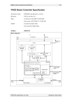
1
usermanual
1-25
Actel Firmware Usermanual
Document Name:
actel_usermanual.doc
Document Revision:
0.2
Firmware Revision:
1.3
Date:
Created on 8/9/2006 9:15:00 AM
Author:
Johan Alme (JA), Ketil Røed (KR)
[email protected]
[email protected]
Last Saved By:
Johan Alme, May 8, 2007
actel_usermanual.doc
Johan Alme & Ketil Røed
usermanual
2-25
ACTEL FIRMWARE USERMANUAL ....................................................................1
1
DOCUMENT CONTROL...................................................................................3
1.1
1.2
1.3
1.4
REVISION HISTORY ..........................................................................................3
REFERENCES ...................................................................................................3
CVS................................................................................................................3
DOWNLOADS...................................................................................................3
2
OVERVIEW.........................................................................................................4
3
ACTEL FIRMWARE GLOBAL REGISTERS................................................5
3.1
3.2
3.3
3.4
4
RCU-SH AND DCS-RCU OPERATION MODES...........................................7
4.1
4.2
4.3
5
COMMAND REGISTER STRUCTURE ..................................................................6
STATUS REGISTER STRUCTURE ........................................................................7
ERROR REGISTER STRUCTURE .........................................................................7
VERSION NUMBER REGISTER STRUCTURE ........................................................7
MEMORY MAPPED MODE .................................................................................8
FLASH MODE .................................................................................................10
SELECTMAP MODE .......................................................................................11
CONFIGURATION OF THE EXTERNAL FLASH DEVICE ....................11
5.1
USING THE SOFTWARE TOOLS .......................................................................11
5.1.1
Prepare for initial configuration & scrubbing ....................................12
5.1.2
Prepare for frame by frame readback and verification .......................13
6
ADVANCED USER ...........................................................................................15
6.1
SOFTWARE TOOLS .........................................................................................15
6.1.1
Rcuflashprog -The RCU Flashprogramer ...........................................15
6.1.2
Framegen – The framegenerator .........................................................16
6.1.3
Framever..............................................................................................17
6.2
HOW TO READ OUT A SINGLE FRAME FROM THE SELECTMAP INTERFACE ....17
6.3
ARCHITECTURE OF EXTERNAL FLASH DEVICE ..............................................21
6.3.1
Setting up Flash device for initial configuration and scrubbing .........22
6.4
PREREQUISITES OF ACTIVE PARTIAL RECONFIGURATION .............................25
actel_usermanual.doc
Johan Alme & Ketil Røed
usermanual
3-25
1 Document control
1.1 Revision history
Rev.
0.1
0.2
0.3
0.4
0.5
Rev. date
02.11.06
08.04.07
Document status
First draft
Small error corrections on address mapping
Responsible
JA/KR
JA
1.2 References
Ref. No.
1
Doc. Name.
Actel specification.doc
Rev / Rev date
0.5/09.08.06
2
Ug012.pdf
V4.0/March 05
3
Ds083.pdf
V4.5/Oct 05
4
MX29LV640BT-BB-1.2.pdf
V1.2/Sep 95
5
ProASICPlus_DS.pdf
V5.0/Aug 05
Title
Digital module requirement
specification
Virtex-II Pro and Virtex-II pro X
User Guide
Virtex-II Pro and Virtex-II pro X
Platfrom FPGAs: Complete
Data Sheet
MX29LV640BT/BB
64M-BIT
[8Mx8/4Mx16] single voltage 3V
Only Flash Memory Data Sheet
ProASICPLUS Flash Family
FPGAs Data Sheet
1.3 CVS
This document and the complete project are checked in to the ALICE CVS database
at the University of Bergen.
Url: http://web.ift.uib.no/kjekscgi-bin/viewcvs.cgi/vhdlcvs/
Module name is rcu_cpld.
1.4 Downloads
Visit http://web.ift.uib.no/~kjeks/wiki for future updates on this document,
programming files and detailed documentation.
actel_usermanual.doc
Johan Alme & Ketil Røed
usermanual
4-25
2 Overview
The solution on the RCU boards consists of a flash-based Actel FPGA that
communicates with the SelectMAP Interface on the Xilinx Virtex-II pro, and an onboard Flash Memory. The Actel FPGA has a communication interface upwards to the
DCS board. All needed configuration files for the Xilinx are stored on the Flash
Memory. Due to the limited access to the Actel for later firmware updates, the main
focus in the development of the firmware has been robustness. Thus as much
functionality as practical possible is handed over to the DCS board.
actel_usermanual.doc
Johan Alme & Ketil Røed
usermanual
5-25
3 Actel firmware global registers
Register name
Address
Type
Description
Command
Size
(bit)
1
0xB000
W
Command_SM
12
0xB002
W
Actel_Reset
Status
Error
Version_Number
Input_Data
1
12
8
16
16
0xB003
0xB100
0xB101
0xB102
0xB103
T
R
R
R
RW
RB_ErrCnt
16
0xB104
R
RB_Err_FrameNumber
12
0xB105
R
RB_FrameNumber
12
0xB106
R
RB_numOfCycles
16
0xB107
R
Stop power up Code
4
0xB112
W
Flash_Interface
_Memory
SelectMAP_Interface
_Memory
512x16
0xB200 –
0xB3FF
0xB400 –
0xB5FF
RW
Writing to this register triggers a
command execution. See Table 3.2
for available commands
Writing to this register triggers a
command
execution
for
the
SelectMAP. See Table 3.3 for
available commands
Asynch reset to Actel device
Status Register. Table 3.4
Error Register. Table 3.5
Firmware version: Table 3.6
Data to write to Actel, decided by
command how it should be
interpreted
Number of Errors found by
readback and verification of Xilinx
Configuration Memory
Last frame number with error (as
given by the sequence stored in the
Flash memory)
Last frame being verified (as given
by the sequence stored in the Flash
memory)
Number of times a complete Frame
by Frame readback (all frames) has
been done.
Writing X”A” to this register
prevents the Actel from trying to
automatically configure the Xilinx if
sm_done is low
RAM block used for Flash
Communication
RAM block used for SelectMAP
Communication
512x16
1
RW
Table 3.1: Externally accessible registers. Registers 0xb104 through 0xb107 are referred to as
information registers.
1
Legend: W=write, R=read, T= write trigger (not physical registers)
actel_usermanual.doc
Johan Alme & Ketil Røed
usermanual
6-25
3.1 Command Register Structure
The normal operation is command based. This means that most functionality is
controlled by command registers that is made available for the DCS board. In addition
an input data register is used as a configuration register for some of the commands.
Command
CLEAR_ERROR
Value
0x1
Data register (0xB103)
Not Used
CLEAR_STAT
INIT_CONFIG
0x2
0x4
Not Used
Not Used
SCRUB
SCRUB_CONT
0x10
0x20
RBFRAME
0x100
Not Used
Num of times to run. If
zero
then
run
continuously until abort.
Not Used
RBFRAME_CONT
0x200
ABORT
0x8000
Num of times to run. If
zero
then
run
continuously until abort.
Not Used
Description
Clears error register, and brings
FW out of an illegal state. Must be
done if error has occurred.
Clears status register and counters
Initial configuration of Xilinx from
Flash
Reconfigures Xilinx one time.
Scrub Continuously from Flash
Read back single frame from Xilinx
and clear error if found.
Continuously read back Xilinx and
clear error if found
Aborts ongoing operation
Table 3.2: Command Register Codes (0xB000). Used for executing the main tasks of the Actel
firmware.
Command SM
Value
INIT_XIL
0x1
Data register
(0xb103)
Not Used
STARTUP_XIL
WRITE_XIL
0x2
0x4
Not Used
Data to be written
READ_XIL
0x8
ABORT_XIL
0x10
Number of 16 bit words
to read. If this register is
0, only 1 read op is
performed.
Not Used
Description
Do init procedure of Xilinx. Will
erase the content of the Xilinx
configuration memory.
Do startup procedure of Xilinx
Write a 16 bit word to SelectMAP
IF
Issue a read command of
SelectMAP IF. (Only effective if
certain write commands been
issued first)
Issue abort sequence
Table 3.3: Command_SM Register Codes (0xB002). The SelectMAP Command register is used
for executing atomic tasks on the SelectMAP bus.
actel_usermanual.doc
Johan Alme & Ketil Røed
usermanual
7-25
3.2 Status register structure
Name
Value of the Stop power up
code register (0xb112)
Null pointer in flash
Bit index
11:8
7
Busy
6
Not used
Smap busy
5
4
(Last) Active code
3:0
Description
0xA: Automatic configuration of Xilinx is
deactivated
0: Flash contains a pointer value
1: Flash contains no pointer value
0: Configuration controller ready to received
command
1: Configuration controller is busy with ongoing
task/command
NA
0: SelectMAP interface module ready
1: SelectMAP interface busy
Contains the last task carried out by the
configuration controller
0xA: Initial configuration
0xB: Scrubbing
0xC: Scrubbing continous
0xD: Read back frame and verify
0xE: Read back frame and verify continuous
Table 3.4: Status register (0xB100).
3.3 Error register structure
Name
SelectMAP RAM parity error
Bit index
7
Flash RAM parity error
6
Not used
Smap unknown command
5:3
2
Smap busy not asserted
1
Smap Done failed
0
Description
0: No parity error
1: Parity error detected in SelectMAP RAM
0: No parity error
1: Parity error detected in Flash RAM
NA
0: Legal command
1: Unknown command issued to Smap interface
0: No errors
1: Busy on SelectMAP interface was not actived
0: Done detected after configuration of Xilinx
1: Failed to detect Done from SelectMAP
interface.
Table 3.5: Error register (0xB101)
3.4 Version number register structure
Name
Major number
Minor number
Bit index
15:8
7:0
Description
For firmware version v1.03 major number this
register will contain the value 0x103
Table 3.6: Version number register (0xB103)
4 Rcu-sh and DCS-RCU operation modes
The RCU Shell is a small command-line software for communicating with the
firmware on the RCU motherboard, that is the Xilinx Virtex-II and Actel firmware. It
is started by simply typing 'rcu-sh' at the command-line. This will bring you to the
actel_usermanual.doc
Johan Alme & Ketil Røed
usermanual
8-25
shell mode, where different types of commands can be executed. Issuing a command
in the rcu-sh software can be done either by writing rcu-sh <command> in the dcs
board linux terminal prompt, or by first starting the rcu-sh software and then write the
<command>.
The RCU motherboard can be operated in three different modes.
1. Memory mapped mode
2. SelectMAP mode
3. Flash mode
The default mode is memory mapped mode, which gives you direct memory access of
the registers in the FPGAs on the RCU motherboard.
Figure 4-1: Sketch showing a logical model of the three modes.From left to right Flash mode,
SelectMAP mode and Mempry mapped mode (normal operation). In Memory Mapped Mode the
RCU Flash Memory is read-only.
Flash mode gives the dcs board direct control of the flash memory on the RCU
motherboard, while SelectMAP mode gives the dcs board direct control over the
SelectMAP interface of the Xilinx Virtex-II on the RCU motherboard.
4.1 Memory mapped mode
Normal operation in memory mapped mode assumes that the flash is setup with
correct pointer information and configuration files and frames. If the on board Flash
device contains no data or incorrect data, section 5 provides more information on
how to proceed. Table 4.1 lists the general commands used to write to and read from
register and memory locations in the Actel firmware.
actel_usermanual.doc
Johan Alme & Ketil Røed
usermanual
Option
Get help on commands:
Single write
Multiple write
Single read
Multiple read
9-25
Command
help
w<rite> 0x[address] 0x[data]
w<rite> 0x[address] <num> 0x[data]
num = number of sequental addresses to write the given data to
r<ead> 0x[address]
r<ead> 0x[address] [num]
num = number of sequental addresses to read
Table 4.1: General rcu-sh commands
The most frequent used commands during normal operation are:
Reading the status, error and other important registers
• By reading back register 0xb100 through 0xb107
r 0xb100 8
Disabling the automatic configuration feature
• By writing 0xa to the stop power up register
w 0xb112 0xa
Clearing error and status registers
• Clearing error register
• Clearing status register
(0xb100 & 0xb104-0xb107)
w 0xb000 0x1
w 0xb000 0x2
and
information
registers
Complete initial configuration of the Xilinx FPGA
• By single command from DCS board
• On power up of the board
• If Xilinx is not configured and the stop code 0xa is not written
to the stop power up code register 0xb112.
w 0xb000 0x4
Active Partial Reconfiguration (Scrubbing) of the complete configuration memory in the Xilinx. It is
issued by a single command from the DCS board and runs either as:
w 0xb000 0x10
• a single reconfiguration
w
0xb000 0x20
• continuously running a given number of cycles or until an abort
is issued
The given number of cycles [num] until an abort must first be written
to the data register. If the data register stores the value 0 the operation
will run continuously until an abort is issued.
w 0xb103 0x[num]
Frame by frame readback and verification, and reconfiguration of a frame if an error is discovered. There
are two possible ways of operation
•
•
stepping through one single frame at the time by a DCS
command, making it possible to read the contents of the
memories from DCS board for more thorough error logging
and handling
continuously running a given number of cycles or until an abort
is issued
w 0xb000 0x100
w 0xb000 0x200
The given number of cycles [num] until an abort must first be written
to the data register. If the data register stores the value 0 the operation
will run continuously until an abort is issued.
w 0xb103 0x[num]
actel_usermanual.doc
Johan Alme & Ketil Røed
usermanual
10-25
Delete the configuration memory of the Xilix Virtex-II FPGA
•
this command activates the prog_b line of the SelectMAP
interface, thereby deleting the content of the configuration
memory of the Xilinx.
w 0xb002 0x0x1
This only works when 0xa is written to the stop power up register
0xb112 to disable automatic reconfiguration of the Xilinx.
Some additional commands exists which are related to communication with the
SelectMAP interface. These commands are recommended use for advanced users
only.
Option
Issue startup procedure of Xilinx
Write a 16 bit word to the SelectMAP IF by first
writing to the data register (0xb103) and then
issuing the command
Issue a read from the SelectMAP IF by first writing
the number of words to read in the data register
(0xb103). If the data register contains 0, only 1
word is read
Command
w 0xb002 0x2
w 0xb103 0x[data]
w 0xb002 0x4
The result will be placed in the actel internal
SelectMAP user memory (RAM) and can be read
out by issuing the command
Issue the SelectMAP abort sequence
r 0xb400 [num]
[num]= number of words to read
w 0xb113 0x[num]
w 0xb002 0x8
W 0xb002 0x10
Table 4.2: Advanced commands related to the SelectMAP interface
4.2 Flash mode
In this mode the firmware on the DCS board gets direct access to the Flash device
control and data bus interface. The following options are available:
Option
Enable flash mode
Disable flash mode
Get help on commands:
Write to single address in flash:
Write a file from a start address in
the flash:
Erase complete flash:
Erase sector:
Read single address from flash
Verify content
memory
of
the
actel_usermanual.doc
flash
Command
flash enable
flash disable
flash help
flash write 0x[address] 0x[data] [num]
num = number of sequental addresses to write the given data to
flash write [-s] 0x[address] file [size]
-s = byteswap enabled
size = number of 16 bit words to write to the flash from
beginning of file.
flash erase all
flash erase sec 0x[sector address]
flash read 0x[address] [num]
num = number of sequental address to read from the given
address.
flash verify 0x[address] file
Verifies that the content of the flash from the given address
matches the content of the given file.
Johan Alme & Ketil Røed
usermanual
11-25
Table 4.3: Available rcu-sh commands in FLASH mode
The command interface to the Flash device is equal to normal operation of rcu-sh only
typing the word flash in front of the command.
When writing to the external flash device it is important to remember that you can
only write zeros – not ones – to the flash memory. This means that if something
wrong is written, then one must erase the sector and rewrite all what is written into it.
It is also very important to not overwrite anything in the areas of the programming
files, as this can cause damage to the Xilinx when configuring it.
4.3 SelectMAP mode
In this mode the firmware on the DCS board gets direct access to the SelectMAP
interface. For the moment this mode only supports initial configuration using the
following command sequence:
1. rcu-sh sm enable
2. cat <bitfile.bit> > /dev/virtex/
3. rcu-sh
sm
disable
5 Configuration of the External Flash Device
The on board Flash memory device plays a key role in the proper operation of the
Actel firmware. Without a correct configuration of this Flash memory the Actel
firmware will not be able to carry out the main tasks of initial configuration,
scrubbing and frame by frame readback and verification.
The external flash device can be configured using a combination of the rcu-sh
software and/or other dedicated software tools. Section 5.1 describes the approach to
configure the external flash device using the dedicated software tools. Section 6.1
gives a detailed description of the software tools.
5.1 Using the software tools
There are 2 available software tools for frame generation and flash programming:
• Framegen – reads back frame data via the SelectMAP interface and generates
the correct frame files to be programmed to the flash
• Rcuflashprog – programs the initial configuration file, the scrubbing file and
the frame files to the correct locations in the flash
The rcuflashprog is used together with a configuration file called flashconf.txt. This
file contains different parameters that can be set according to which operation that
will be carried out. That is, one can choose to program the configuration file, the
scrubbing file, or the frame files separately, or a combination of these files. This is
done by setting the different enabling parameters connected to the respective files to
either true or false.
actel_usermanual.doc
Johan Alme & Ketil Røed
usermanual
12-25
5.1.1 Prepare for initial configuration & scrubbing
Software tools
Rcuflashprog
Configuration files
Flashconf.txt
Rcu.bit (or other confirguration file)
Rcu_apr.bit (or other scrubbing file)
Comments
The default setting is to erase
the full content of the flash
Enable the init program file and scrubbing file settings and disable the frame file
settings in the flashconf.txt file:
enable_icfile = true(enable programming of initial configurationfile)
enable_scfile = true (enable programming of scrubbing file)
enable_frfiles = false (disable programming of frame files)
The path and filename have default settings and must be changed if other paths or
filenames are used. It is however not recommended to change any other default values
such as for instance the start addresses. This may lead to incorrect configuration of the
flash device and possible failure in the firmware operation.
----------RCU Flashprogramer config file-------------------#enable erase
enable_erase = true
#init program file
enable_icfile = true
path_icfile = /mnt/dcsshare/
name_icfile = rcu.bit
startaddr_icfile = 8000h
#scrubbing file
enable_scfile = true
path_scfile = /mnt/dscshare/
name_scfile = rcu_apr.bit
startaddr_scfile = 60000h
#frame file
enable_frfiles = false
path_frfiles = /mnt/dcsshare/
name_rawframefile = frame$.hex
name_readframefile = r_frame$.hex
name_writeframefile = w_frame$.hex
framesfile = frames.txt
startaddr_frfiles = 100000h
frame_offset = 2h
header_size_read = 1Bh
footer_size_read = 0Bh
------------------------------------------------------------
Save changes and type the command: “./rcuflashprog flashconf.txt” in the command
prompt. The file(s) will now be programmed to the flash. To configure the Xilinx
Virtex-II with the new initial configuration file type the command:
“rcu-sh w 0xb000 0x4” in the command prompt.
See section 6 for information on the scrubbing feature of the firmware.
actel_usermanual.doc
Johan Alme & Ketil Røed
usermanual
13-25
5.1.2 Prepare for frame by frame readback and verification
Software tools
Framegen
Rcuflashprog
Configuration files
frames.txt
read_header.txt
read_footer.txt
write_header.txt
write_footer.txt
Flashconf.txt
Rcu.bit (or other configuration file)*
Rcu_apr.bit (or other scrubbing file)*
frames.txt
frame$.hex
r_frame$.hex
w_frame$.hex
Comments
The Xilinx virtex-II must be
configured with the proper
firmware
The default setting is to erase
the full content of the flash.
*Optional: the programming of the initial configuration file or scrubbing file can be
disabled.
5.1.2.1 Framegen
In order to prepare for frame by frame readback and verification the different frame
files must be generated. This is carried out by the framegen software tool. It reads out
the frames specified in the frames.txt file from the Xilinx Virtex-II. The frames are
stored as hex files in 3 different groups:
•
original frame data: frame$.hex
•
read frame data: r_frame$.hex (read_header.txt & read_footer.txt are added)
•
write fram data: w_frame$.hex (read_header.txt & read_footer.txt are added)
See section 6.1.2 for more information about the configuration files.
Before the framegen software is started make sure that the Xilinx Virtex-II is
configured with the correct firmware. It is also important to check if you can
communicate with the Actel Device and the Flash Device. If you get errors when
doing this, the Xilinx DCS interface is not correct.
Start the framegen software with the command:
"./framegen frames.txt
write_footer.txt"
read_header.txt
read_footer.txt
write_header.txt
Depending on the number of frames to be generated (specified in frames.txt) this
operation may take several minutes.
5.1.2.2 Rcuflashprog
Enable the frame file settings in the flashconf.txt file:
enable_frfiles = true
As for initial configuration and scrubbing use default values unless other paths and
filenames are used.
actel_usermanual.doc
Johan Alme & Ketil Røed
usermanual
14-25
Save changes and type the command: “./rcuflashprog flashconf.txt” in the command
prompt. The file(s) will now be programmed to the flash. To configure the Xilinx
Virtex-II with the new initial configuration file type the command:
“rcu-sh w 0xb000 0x4” in the command prompt. The Xilinx will now be
programmed. See section 6 for information on the frame by frame readback and
verification feature of the firmware.
actel_usermanual.doc
Johan Alme & Ketil Røed
usermanual
15-25
6 Advanced User
6.1 Software tools
The Actel firmware gives the 3 options of initial configuration, scrubbing and frame
by frame readback and verification.
Operation
Initial configuration
Scrubbing
Frame by frame R&V
Need file(s) in flash
Full configuration bit file
Software tool
Rcu-sh
Rcuflashprog*
Scrubbing configuration bit Rcu-sh
file
Rcuflashprog*
Rcubitfileprog
Write frame files
Framegen*
Read frame files
Rcuflashprog*
framever
Figure 6-1: The table lists the different software tools that can be used to configure the external
flash device.
6.1.1 Rcuflashprog -The RCU Flashprogramer
-----------------------------------------------The RCU Flash Programer is a Tool for programing the RCU Flash memory.
It is configurable through a config file which can be specified as a parameter.
"./rcuflashprog flashconf.txt"
An example of the configuration file can be found at the end of this README file.
For the initial config:
the initial configurationfile and the path to the initial configurationfile have to be set.
Also the startaddress for the initial configuration.
For the scrubbing:
The scrubbingfile and the path to the scrubbingfile have to be set, also the the start
address for the scrubbing.
For the flash programing of the frames:
The path for the framefiles has to be set, also there have to be all the frames specified
in the framesfile.
the three "name_" variables define the filename of the framefiles. The $ is therefore
replaced with "X.Y.Z" where X is the Block, Y is the Major and Z the Minornumber.
The startaddress has to be defined, also the size of the readheader and the readfooter.
actel_usermanual.doc
Johan Alme & Ketil Røed
usermanual
16-25
----------RCU Flashprogramer config file-------------------#init program file
enable_icfile = true
path_icfile = /mnt/kjekspc4/dominik/bin/rcuflashprog/
name_icfile = initconfig.bit
startaddr_icfile = 0h
#scrubbing file
enable_scfile = true
path_scfile = /mnt/kjekspc4/dominik/bin/rcuflashprog/
name_scfile = scrubbing.bit
startaddr_scfile = 60000h
#frame file
enable_frfiles = true
path_frfiles = /mnt/kjekspc4/dominik/bin/rcuflashprog/
name_rawframefile = frame$.hex
name_readframefile = r_frame$.hex
name_writeframefile = w_frame$.hex
framesfile = frames.txt
startaddr_frfiles = 100000h
frame_offset = 2h
header_size_read = 1Bh
footer_size_read = 0Bh
------------------------------------------------------------
6.1.2 Framegen – The framegenerator
In order to prepare for frame by frame readback and verification the different frame
files must be generated. This is carried out by framegen software tool.
The Framegenerator is a Tool for reading out frames from Xilinx configuration
memory.
To run it 5 input files are needed:
• Frames file (i.e. frames.txt)
• Read header file (i.e. read_header.txt)
• Read footer file (i.e. read_footer.txt)
• Write header file (i.e. write_header.txt)
• Write footer file (i.e. write_footer.txt)
These files have to be given to the program on startup as parameters, i.e.:
"./framegen frames.txt read_header.txt read_footer.txt write_header.txt
write_footer.txt"
The frames file contains the framenumbers coded in Block, Major and Minornumber.
The syntax in the frames file is like this: "Block;Major;Minor;"
i.e.:
actel_usermanual.doc
Johan Alme & Ketil Røed
usermanual
17-25
0;5;3;
0;5;4;
The header and footer files contain the commands to be executed before/after reading
of a frame. Also this data is included in the created readback files. The addresses of
the frames have to be inserted as variables into this file ("frame_addr31_16" and
"frame_addr15_0"). The proper addresses for the frame will be inserted here by the
program.
For every frame it creates three files:
• one file with the raw readback data
• one file with the read header before the data and the read footer after the data
• one file with the write header before the data and the write footer after the data
6.1.3 Framever
The framever is used to run a more thorough readback and verification operation from
the DCS board. The tool makes it possible to the location of the actually SEUs within
the individual frames.
The tool will not be discussed in this version of the user manual.
6.2 How to read out a single frame from the SelectMAP
interface
A full frame read back via the SelectMAP interface carry out by first writing a
sequence of header data to the SelectMAP interface, then reading back the frame
content before closing with a sequence of footer data. The header and footer data are
special commands for preparing the SelectMAP interface for a frame read back
FFFFFFFF
AA995566
30008001
00000007
30016001
00000069
30008001
00000004
30002001
$frameaddr
28006000
480000D4
20000000
20000000
#
#
#
#
#
#
#
#
#
#
#
#
#
#
Sync word
Type 1 header: Write 1 word to cmd-register
Reset CRC
Type 1 header: Write 1 word to frame-length register
Set frame length
Type 1 header: Write 1 word to cmd-register
Read configuration data command
Write frame address command
Frame address (ex: clb – major 5 – minor 3)
Type 1 header: Read from Configuration Out reg. (FDRO)
Type 2 header: Read 212 words from FDRO
NOOPs to flush the register
Table 6.1: Read frame header. This table is based on table 4-37 in the Virtex-II FPGA user guide
(Ref No. 2), without the commands related to the shutdown.
actel_usermanual.doc
Johan Alme & Ketil Røed
usermanual
30008001
00000007
30008001
0000000D
20000000
20000000
18-25
#
#
#
#
#
#
Type 1 header: Write 1 word to cmd-register
Reset CRC
Type 1 header: Write 1 word to cmd-register
de synch interface
NOOPs to flush the register
Table 6.2: Read frame footer. This table is based on table 4-37 in the Virtex-II FPGA user guide
(Ref No. 2), without the commands related to the shutdown.
In between the header and footer the read back frame file is stored. The data must be
ordered following a Big Endean 16 bit system.
The frames have the following address composition:
31:27
00000
BA
26:25
XX
MJA
24:17
XXXXXXXX
MNA
16:9
XXXXXXXX
Byte number
8:0
000000000
Table 6.3: Virtex-II Pro frame address composition
See the Virtex-II FPGA user guide (Ref No. 2) for more information on addressing
the different frames and reading and writing frame data.
In order to write data to the SelectMAP interface the following rcu-sh commands are
use:
W 0xb103 0x[data] (write data to actel data register)
W 0xb002 0x4
(issue a write of data to the SelectMAP IF)
In Table 6.4 an rcu-sh script example is given for reading out a single frame. This
example is for a CLB (BA: 00) with MJA 3 and MNA 2 which gives the address
0x00060400.
actel_usermanual.doc
Johan Alme & Ketil Røed
usermanual
19-25
#write header commands
w 0xb103 0xffff
w 0xb002 0x4
w 0xb103 0xffff
w 0xb002 0x4
w 0xb103 0xaa99
w 0xb002 0x4
w 0xb103 0x5566
w 0xb002 0x4
w 0xb103 0x3000
w 0xb002 0x4
w 0xb103 0x8001
w 0xb002 0x4
w 0xb103 0x0000
w 0xb002 0x4
w 0xb103 0x0007
w 0xb002 0x4
w 0xb103 0x3001
w 0xb002 0x4
w 0xb103 0x6001
w 0xb002 0x4
w 0xb103 0x0000
w 0xb002 0x4
w 0xb103 0x0069
w 0xb002 0x4
w 0xb103 0x3000
w 0xb002 0x4
w 0xb103 0x8001
w 0xb002 0x4
w 0xb103 0x0000
w 0xb002 0x4
w 0xb103 0x0004
w 0xb002 0x4
w 0xb103 0x3000
w 0xb002 0x4
w 0xb103 0x2001
w 0xb002 0x4
#[$frame_addr32_16]
w 0xb103 0x0006
w 0xb002 0x4
#[$frame_addr32_16]
w 0xb103 0x0400
w 0xb002 0x4
w 0xb103 0x2800
w 0xb002 0x4
w 0xb103 0x6000
w 0xb002 0x4
w 0xb103 0x4800
w 0xb002 0x4
w 0xb103 0x00d4
w 0xb002 0x4
w 0xb103 0x2000
w 0xb002 0x4
w 0xb103 0x0000
w 0xb002 0x4
w 0xb103 0x2000
w 0xb002 0x4
w 0xb103 0x0000
w 0xb002 0x4
#issue multiple read 212x2=424 (0x1a8) 16 bits words to account for pad/data frame
w 0xb103 0x1a8
actel_usermanual.doc
Johan Alme & Ketil Røed
usermanual
20-25
w 0xb002 0x8
#write footer commands
w 0xb103 0x3000
w 0xb002 0x4
w 0xb103 0x8001
w 0xb002 0x4
w 0xb103 0x0000
w 0xb002 0x4
w 0xb103 0x0007
w 0xb002 0x4
w 0xb103 0x3000
w 0xb002 0x4
w 0xb103 0x8001
w 0xb002 0x4
w 0xb103 0x0000
w 0xb002 0x4
w 0xb103 0x000D
w 0xb002 0x4
w 0xb103 0x2000
w 0xb002 0x4
w 0xb103 0x0000
w 0xb002 0x4
w 0xb103 0x2000
w 0xb002 0x4
w 0xb103 0x0000
w 0xb002 0x4
Table 6.4: rcu-sh script commands for reading out a single frame via the SelectMAP interface.
This example is for frame address 0x00060400 which is BA:00, MJA:3 and MNA:2.
A single frame consists of 106 words of 32 bits. In order to account for the internal
frame buffer in the SelectMAP interface, it is necessary to first read back one extra
frame which is known as a pad frame. Since the DCS-RCU interface is a 16 bit
interface this means that 106 x 2 = 212 words of 16 bits must be read back for one
frame.
After executing the script in Table 6.4 the both the pad frame data and frame data is
available from the SelectMAP internal RAM memory in the Actel. To read out a
formatted version of the frame data type the commands in Table 6.5.
Command
rcu-sh r 0xb4d4 –f
%b2 -o framefile.hex
od –x framefile.hex
Description
Write binary data to a file
View the file
Table 6.5: Commands for reading out formatted frame data
actel_usermanual.doc
Johan Alme & Ketil Røed
usermanual
21-25
6.3 Architecture of External Flash Device
Data-location
Configuration pointer
Scrubbing pointer
Read Frame pointer
Default mode pointer (NOT USED)
Function
Pointer space. Each pointer is 4 bytes (2 word
addresses). The different pointers points to
addresses where more information is stored.
Configuration data start (word)-address
Configuration data stop (word)-address
Info space: Start and stop address for initial
configuration data stream. The addresses are
given in word addresses
Scrubbing data start (word)-address
Scrubbing data stop (word)-address
Start and stop address for scrubbing data stream.
The addresses are given in word addresses
FRAME FILE INFO
Start address (22 bit)
Frame offset (3 bit)
Number of frames (12 bit)
Read frame size (8 bit)
Write frame size (9 bit)
Read header size (8 bit)
Read footer size (8 bit)
Start address of read frame
Relative address jump to next read frame
Number of frames to read back
Size of read frame data
Size of write frame data including header/footer
Size of read header
Size of read footer
See Table 6.7 for detailed information
Configuration data file
File space. The actual files are stored here. The
commands needed for the Xilinx to understand
the frame files are included as headers and
footers in the actual files.
Scrubbing data file
READ BLOCK
Read – Frame header 1
Read – Data frame 1
Read – Frame Footer 1
.
Read – Frame header N
Read – Data frame N
Read – Frame Footer N
The write frame files will always be located the
address:
Read-frame start address + 0x100000
Example: If the address of the first read frame
0x100000 the corresponding write frame will be
located at address 0x200000.
WRITE BLOCK
Write – Frame header 1
Write – Data frame 1
Write – Frame Footer 1
.
Write – Frame header N
Write – Data frame N
Write – Frame Footer N
Table 6.6: The Flash memory is divided into to three different spaces, as described below.
The Flash device is divided into to 3 different spaces:
1. The pointer space. This is located in the start of the Flash memory, and
contains pointers to location in the info space. The addresses of the pointers
are pre-defined, and a zero value in the pointer means that the given file does
not exist in the Flash memory. The default mode pointer contains a pointer to
one of the three other pointer locations.
actel_usermanual.doc
Johan Alme & Ketil Røed
usermanual
22-25
2. The info space. This section contains the address location of the initial
configuration data file and the scrubbing data file. It also contains the address
location and various frame information for the frame files.
3. The file space: In the section of the flash all the different files are stored. That
is configuration data file, the scrubbing data file and the all the frame files
needed for frame by frame readback and verification (both read-frame and
write-frame files)
Table 6.7 gives the detailed location of the frame related information in the flash
memory. The information is stored in 16 bit words. Relative address position 0 and 1
holds the 6 MSB and 16 LSB of the read frame start address. During initial
configuration address position 2 and 3 holds the stop address of the configuration
data. However this information is not used during readback and verification. Further
frame information is stored in the three consecutive flash address positions.
Rel. Content
Addr.
0
File-space start address
1
File-space start address
2
File-space stop address
3
File-space stop address
4
Frame info register 1
5
Frame info register 2
6
Frame info register 3
* MSB of write frame size
Bit position
15 14 13 12 11 10 9 8 7 6 5 4 3 2 1 0
Not used
6 MSB
16 LSB
Not used
(6 MSB)
Not used (16 LSB)
frame offset
number of frames
*
read frame size - 1
write frame size - 1
Read header size - 1
Read footer size - 1
Table 6.7: Overview of frame information content in the Flash Memory Device.
6.3.1 Setting up Flash device for initial configuration and
scrubbing
Example case:
• Initial configuration file top_level.bit of size 560751 bytes
• Scrubbing file top_level_scrub.bit of size
Setting up Pointer Space and Info Space
The addresses of the pointers are pre-defined, and a value of 0xFFFF in the pointer
means that the given file does not exist in the Flash memory.
Pointer
Init Config Pointer
Scrubbing Pointer
Frame pointer
Address (BB type Flash)
0x000000 – Info space start address [21:16]
0x000001 – Info space start address [15:0]
0x001000 – Info space start address [21:16]
0x001001 – Info space start address [15:0]
0x002000 – Info space start address [21:16]
0x002001 – Info space start address [15:0]
Table 6.8: Pointers and their physical addresses in the BB type Flash Device. Please note that all
pointers are in separate sectors in the Flash Memory Device, making it possible to delete only one
pointer while keeping the rest. For sector addresses, look in ref 4, table “MX29LV640BT Sector
Group Architecture” and column (x16) Address range.
actel_usermanual.doc
Johan Alme & Ketil Røed
usermanual
23-25
The pointer locations contain the addresses of the respective file space information.
Though these addresses can be any addresses on the Flash device it is convenient to
specify some default addresses to use.
Type of info space
Start address
Type of flash
Init config
0x3000
BB
Scrubbing
0x4000
BB
Frame
0x5000
BB
Table 6.9: Default addresses of the different info spaces.
In order to setup the Info Space one must have the following information
• Start address of the files in the Flash Memory. This can be any address.
o Start address of initial configuration file (i.e. 0x0)
o Start address of scrubbing file (i.e. 0x50000)
o Start address of read frame files (i.e. 0x100000)
• Stop address of the initial configuration and scrubbing file in the Flash
Memory. This can be calculated from the file size and the start address. If the
file is 10 bytes, it is written over 5 addresses, i.e. the stop address is:
o 0x<stop addr> = 0x<start addr> + 0x<byte/2> – 1
• Pointer address. This is given in Error! Reference source not found..
It is also important to remember the ‘-s’ switch when writing the file to the flash
memory as this swap the bytes so that they are injected in the correct order.
flash
flash
flash
flash
flash
flash
flash
flash
flash
flash
flash
flash
flash
flash
flash
flash
enable
# Enables flash mode
w 0x0 0x0
# set up init config pointer
w 0x0 0x3000
# position of start address
w 0x3000 0x0
# start address(21:16) of init cfg file
w 0x3001 0x8000
# start address(15:0) of init cfg file
w 0x3002 0x5
# stop address(21:16) of init cfg file
w 0x3003 0x2736
# stop address(15:0) of init cfg file
w –s 0x8000 <bitfile> # Initial configuration file.
w 0x0 0x0
# set up scrubbing pointer
w 0x1000 0x4000
# position of start address
w 0x4000 0x5
# start address(21:16) of scrubbing file
w 0x4001 0x0000
# start address(15:0) of scrubbing file
w 0x4002 0x7
# stop address(21:16) of scrubbing file
w 0x4003 0x8B88
# stop address(15:0) of scrubbing file
w –s 0x60000 <bitfile> # Scrubbing file
disable
# Disables flash mode
Figure 6-2: Script for setting up initial configuration file and scrubbing file on Flash Memory
Device with pointer and start and stop addresses.
6.3.1.1 Sector Addresses in Flash Memory Device
This information is extracted from ref. 4, table MX29LV640BB Sector Group
Architecture on page 6.
actel_usermanual.doc
Johan Alme & Ketil Røed
usermanual
Sec.
0
1
2
3
4
5
6
7
8
9
10
11
12
13
14
15
16
17
18
19
20
21
22
23
24
25
26
27
28
29
30
31
32
33
34
35
36
37
38
39
40
41
42
43
44
Address range (hex)
0 – FFF
1000 – 1FFF
2000 – 2FFF
3000 – 3FFF
4000 – 4FFF
5000 – 5FFF
6000 – 6FFF
7000 – 7FFF
8000 – FFFF
10000 – 17FFF
18000 – 1FFFF
20000 – 27FFF
28000 – 2FFFF
30000 – 37FFF
38000 – 3FFFF
40000 – 47FFF
48000 – 4FFFF
50000 – 57FFF
58000 – 5FFFF
60000 – 67FFF
68000 – 6FFFF
70000 – 77FFF
78000 – 7FFFF
80000 – 87FFF
88000 – 8FFFF
90000 – 97FFF
98000 – 9FFFF
A0000 – A7FFF
A8000 – AFFFF
B0000 – B7FFF
B8000 – BFFFF
C0000 – C7FFF
C8000 – CFFFF
D0000 – D7FFF
D8000 – DFFFF
E0000 – E7FFF
E8000 – EFFFF
F0000 – F7FFF
F8000 – FFFFF
100000 – 107FFF
108000 – 10FFFF
110000 – 117FFF
118000 – 11FFFF
120000 – 127FFF
128000 – 12FFFF
24-25
Sec.
45
46
47
48
49
50
51
52
53
54
55
56
57
58
59
60
61
62
63
64
65
66
67
68
69
70
71
72
73
74
75
76
77
78
79
80
81
82
83
84
85
86
87
88
89
Address range (hex)
130000 – 137FFF
138000 – 13FFFF
140000 – 147FFF
148000 – 14FFFF
150000 – 157FFF
158000 – 15FFFF
160000 – 167FFF
168000 – 16FFFF
170000 – 177FFF
178000 – 17FFFF
180000 – 187FFF
188000 – 18FFFF
190000 – 197FFF
198000 – 19FFFF
1A0000 – 1A7FFF
1A8000 – 1AFFFF
1B0000 – 1B7FFF
1B8000 – 1BFFFF
1C0000 – 1C7FFF
1C8000 – 1CFFFF
1D0000 – 1D7FFF
1D8000 – 1DFFFF
1E0000 – 1E7FFF
1E8000 – 1EFFFF
1F0000 – 1F7FFF
1F8000 – 1FFFFF
200000 – 207FFF
208000 – 20FFFF
210000 – 217FFF
218000 – 21FFFF
220000 – 227FFF
228000 – 22FFFF
230000 – 237FFF
238000 – 23FFFF
240000 – 247FFF
248000 – 24FFFF
250000 – 257FFF
258000 – 25FFFF
260000 – 267FFF
268000 – 26FFFF
270000 – 277FFF
278000 – 27FFFF
280000 – 287FFF
288000 – 28FFFF
290000 – 297FFF
Sec.
90
91
92
93
94
95
96
97
98
99
100
101
102
103
104
105
106
107
108
109
110
111
112
113
114
115
116
117
118
119
120
121
122
123
124
125
126
127
128
129
130
131
132
133
134
Address range (hex)
298000 – 29FFFF
2A0000 – 2A7FFF
2A8000 – 2AFFFF
2B0000 – 2B7FFF
2B8000 – 2BFFFF
2C0000 – 2C7FFF
2C8000 – 2CFFFF
2D0000 – 2D7FFF
2D8000 – 2DFFFF
2E0000 – 2E7FFF
2E8000 – 2EFFFF
2F0000 – 2F7FFF
2F8000 – 2FFFFF
300000 – 307FFF
308000 – 30FFFF
310000 – 317FFF
318000 – 31FFFF
320000 – 327FFF
328000 – 32FFFF
330000 – 337FFF
338000 – 33FFFF
340000 – 347FFF
348000 – 34FFFF
350000 – 357FFF
358000 – 35FFFF
360000 – 367FFF
368000 – 36FFFF
370000 – 377FFF
378000 – 37FFFF
380000 – 387FFF
388000 – 38FFFF
390000 – 397FFF
398000 – 39FFFF
3A0000 – 3A7FFF
3A8000 – 3AFFFF
3B0000 – 3B7FFF
3B8000 – 3BFFFF
3C0000 – 3C7FFF
3C8000 – 3CFFFF
3D0000 – 3D7FFF
3D8000 – 3DFFFF
3E0000 – 3E7FFF
3E8000 – 3EFFFF
3F0000 – 3F7FFF
3F8000 – 3FFFFF
Table 6.10: Sector addresses in the BB type Flash Device. To erase a sector, address the start
address of the sector you want to erase. The first sectors given with grey background (sec 0 – 7)
are smaller sectors in the boot partition of the Flash. These sectors are used as the pointer space
(and most often as info space) in the application.
actel_usermanual.doc
Johan Alme & Ketil Røed
usermanual
25-25
6.4 Prerequisites of Active Partial Reconfiguration
The RCU consist of a Xilinx Virtex-2 Pro vp7, with an Actel device communicating
with the Selectmap Interface of the Xilinx FPGA. The firmware inside the Actel has
the possibility to both read and write to the configuration logic using slave selectMAP
mode.
The Actel firmware supports main features:
• To read back all block num 0 and block num 2 frames continuously and
overwrite any of these if an error is seen. The frames are first read back in a
controlled setup and stored to be used as comparison.
• Use the active partial reconfiguration file generated by ISE to continuously
overwrite the configuration memory.
To be able to do this some precautions needs to be made at design time of the Xilinx
design:
1. The input LUT of the Slices cannot be used as writable memory elements.
Practically this means to unselect ‘shift register extraction’ under HDL options
in the Synthesis menu, as well as choosing to extract memory elements to
BRAM..
2. The first BRAM major frame must not be used. Practically this is to not use
the very first BRAM slices, which is done by the use of the CONFIG
PROHIBIT argument in the ucf file (as shown below).
CONFIG
CONFIG
CONFIG
CONFIG
CONFIG
CONFIG
CONFIG
CONFIG
CONFIG
CONFIG
CONFIG
CONFIG
CONFIG
CONFIG
CONFIG
CONFIG
CONFIG
CONFIG
CONFIG
CONFIG
PROHIBIT
PROHIBIT
PROHIBIT
PROHIBIT
PROHIBIT
PROHIBIT
PROHIBIT
PROHIBIT
PROHIBIT
PROHIBIT
PROHIBIT
PROHIBIT
PROHIBIT
PROHIBIT
PROHIBIT
PROHIBIT
PROHIBIT
PROHIBIT
PROHIBIT
PROHIBIT
=
=
=
=
=
=
=
=
=
=
=
=
=
=
=
=
=
=
=
=
RAMB16_X0Y9;
MULT18X18_X0Y9;
RAMB16_X0Y8;
MULT18X18_X0Y8;
RAMB16_X0Y7;
MULT18X18_X0Y7;
RAMB16_X0Y6;
MULT18X18_X0Y6;
RAMB16_X0Y5;
MULT18X18_X0Y5;
RAMB16_X0Y4;
MULT18X18_X0Y4;
RAMB16_X0Y3;
MULT18X18_X0Y3;
RAMB16_X0Y2;
MULT18X18_X0Y2;
RAMB16_X0Y1;
MULT18X18_X0Y1;
RAMB16_X0Y0;
MULT18X18_X0Y0;
3. The selectMAP pins must be set to persist.
4. Bit files should be generated using the following bitgen commands:
a. Initial configuration file:
bitgen -w -d -g Persist:Yes Xilinx_RCU_FW_190606/rcu.ncd rcu.bit
b. Active partial reconfiguration (scrubbing) file:
bitgen -w -d -g Compress -g Persist:Yes -g ActiveReconfig:Yes -g
PartialMask0:7fffffffff -g PartialMask1:0 -g PartialMask2:3F
Xilinx_RCU_FW_190606/rcu.ncd rcu_apr.bit
actel_usermanual.doc
Johan Alme & Ketil Røed