1
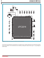
All MikroElektronika´s development systems represent irreplaceable
tools for programming and developing microcontroller-based devices.
Carefully chosen components and the use of machines of the last
generation for mounting and testing thereof are the best guarantee of
high reliability of our devices. Due to simple design, a large number of
add-on modules and ready to use examples, all our users, regardless
of their experience, have the possibility to develop their project in a fast
and efficient way.
User manual
Development system
™
If you have any questions, comments or business proposals, do not hesitate to contact us at [email protected]
If you are experiencing some problems with any of our products or just need additional information, please place your ticket at
www.mikroe.com/en/support
If you want to learn more about our products, please visit our website at www.mikroe.com
mikroBoard for ARM 144-pin
DISCLAIMER
All the products owned by MikroElektronika are protected by copyright law and international copyright treaty.
Therefore, this manual is to be treated as any other copyright material. No part of this manual, including
product and software described herein, may be reproduced, stored in a retrieval system, translated or
transmitted in any form or by any means, without the prior written permission of MikroElektronika. The
manual PDF edition can be printed for private or local use, but not for distribution. Any modification of this
manual is prohibited.
TO OUR VALUED CUSTOMERS
I want to express my thanks to you for being interested in our products and for having confidence in
Mikroelektronika.
The primary aim of our company is to design and produce high quality electronic products and to constantly
improve the performance thereof in order to better suit your needs.
Nebojsa Matic
General Manager
MikroElektronika provides this manual ‘as is’ without warranty of any kind, either expressed or implied,
including, but not limited to, the implied warranties or conditions of merchantability or fitness for a particular
purpose.
MikroElektronika shall assume no responsibility or liability for any errors, omissions and inaccuracies that may
appear in this manual. In no event shall MikroElektronika, its directors, officers, employees or distributors be
liable for any indirect, specific, incidental or consequential damages (including damages for loss of business
profits and business information, business interruption or any other pecuniary loss) arising out of the use
of this manual or product, even if MikroElektronika has been advised of the possibility of such damages.
MikroElektronika reserves the right to change information contained in this manual at any time without prior
notice, if necessary.
HIGH RISK ACTIVITIES
The products of MikroElektronika are not fault – tolerant nor designed, manufactured or intended for use or
resale as on – line control equipment in hazardous environments requiring fail – safe performance, such as
in the operation of nuclear facilities, aircraft navigation or communication systems, air traffic control, direct
life support machines or weapons systems in which the failure of Software could lead directly to death,
personal injury or severe physical or environmental damage (‘High Risk Activities’). MikroElektronika and its
suppliers specifically disclaim any expressed or implied warranty of fitness for High Risk Activities.
TRADEMARKS
The Mikroelektronika name and logo, the Mikroelektronika logo, mikroC, mikroC PRO, mikroBasic, mikroBasic PRO, mikroPascal, mikroPascal PRO, AVRflash, PICflash, dsPICprog, 18FJprog, PSOCprog, AVRprog, 8051prog, ARMflash, EasyPIC5, EasyPIC6, BigPIC5, BigPIC6, dsPIC PRO4, Easy8051B, EasyARM,
EasyAVR5, EasyAVR6, BigAVR2, EasydsPIC4A, EasyPSoC4, EasyVR Stamp LV18FJ, LV24-33A, LV32MX,
PIC32MX4 MultiMedia Board, PICPLC16, PICPLC8 PICPLC4, SmartGSM/GPRS, UNI-DS are trademarks
of Mikroelektronika. All other trademarks mentioned herein are property of their respective companies.
All other product and corporate names appearing in this manual may or may not be registered trademarks
or copyrights of their respective companies, and are only used for identification or explanation and to the
owners’ benefit, with no intent to infringe.
The NXP name, logo and products names are trademarks of NXP Inc. in the U.S.A and other countries.
©MikroelektronikaTM, 2011 All Rights Reserved.
3
page
mikroBoard for ARM 144-pin
TABLE OF CONTENTS
1. General information ...................................................................................................................... 4
2. LPC2214 microcontroller .............................................................................................................. 5
3. Programming the microcontroller ................................................................................................. 8
4. Voltage regulator ..........................................................................................................................13
5. MicroSD connector .......................................................................................................................14
6. Flash module ................................................................................................................................15
MikroElektronika
page
4
mikroBoard for ARM 144-pin
1. General information
MikroBoard for ARM 144-pin is primarily intended to be connected to the EasyARM v6 development system but can
also be used as a stand-alone device. The board features the LPC2214 microcontroller, flash module, USB connector,
microSD connector, JTAG connector, USB UART, voltage regulator and connectors that enable connection with the
development system.
Figure 1-1: mikroBoard for ARM 144-pin
MikroElektronika
5
page
mikroBoard for ARM 144-pin
2. LPC2214 microcontroller
The LPC2214 microcontroller in 144-pin LQFP package is soldered on the mikroBoard for ARM 144-pin. Some of its
key features are:
- 16/32-bit ARM7TDMI-S microcontroller in a LQFP144 package
- 16 kB on-chip static RAM and 256 kB on-chip flash program memory. 128-bit wide interface/
accelerator enables high speed 60 MHz operation.
- In-System Programming (ISP) and In-Application Programming (IAP) via on-chip bootloader software.
Figure 2-1: LPC2214 microcontroller
LPC2214 is connected to on board modules via pins which are also connected to CN1 and CN2 connectors. These two
connectors enable the board to be connected to the EasyARM v6 development system or some other device.
MikroElektronika
6
page
mikroBoard for ARM 144-pin
VCC-3.3
R13
1K
RESET
D1
1N4148
T1
X1
14.74568MHz
VCC-3.3
VCC-3.3
VCC-3.3
VCC-3.3
VCC-3.3
VCC-3.3
VCC-3.3
C3
C4
C5
C6
C7
C8
C9
100nF
100nF
100nF
100nF
100nF
100nF
100nF
VCC-1.8
C2
22pF
P1.27
22pF
VCC-1.8
V18A
XTAL1
XTAL2
P1.28
GND
GNDA-PPL
P2.21
P2.20
RESET
P2.19
P2.18
P2.17
P2.16
P2.15
P2.14
GND
P2.13
P1.29
P2.12
P2.11
P0.20
P0.19
P0.18
P2.10
V3
P2.9
P2.8
P2.7
P2.6
P2.5
P1.30
V3
GND
V18
P2.4
C1
100
MCU-RST#
R14
C22
100nF
P2.22
VCC-3.3
C10
100nF
VCC-3.3
C11
100nF
VCC-3.3
C12
100nF
VCC-3.3
C13
LPC2214
P2.3
GND
P2.2
P2.1
V3
GND
P1.20
P0.17
P0.16
P0.15
P2.0
P3.30
P3.31
P1.21
V3
GND
P0.14
P1.0
P1.1
P3.0
P3.1
P3.2
P1.22
P0.13
P0.12
P0.11
P1.23
P3.3
P3.4
GND
P0.10
V3
P0.9
P0.8
P3.5
P3.6
V18
GND
V3
P3.23
P3.22
P0.0
P1.31
P3.21
P3.20
P3.19
P3.18
P3.17
P0.1
P0.2
V3
P1.26
P3.16
GND
P3.15
P3.14
V3
P0.3
P0.4
P1.25
P0.5
P3.13
P3.12
P3.11
P3.10
P3.9
GND
P0.6
P0.7
P1.24
P3.8
P3.7
100nF
V3
GND
P0.21
P0.22
P0.23
P1.19
P0.24
GND
P2.23
P2.24
P2.25
P2.26
V3A
P1.18
P2.27
P2.28
P2.29
P2.30
P2.31
P0.25
NC
P0.27
P1.17
P0.28
GND
P3.29
P3.28
P3.27
P3.26
V3
P0.29
P0.30
P1.16
P3.25
P3.24
VCC-1.8
VCC-3.3
VCC-3.3
R7
10K
VCC-3.3
R8
10K
VCC-1.8
C14
100nF
VCC-1.8
C15
100nF
VCC-1.8
C16
100nF
Figure 2-2: LPC2214 microcontroller with oscillators connection schematic
The LPC2214 microcontroller is connected to the X1 oscillator. The X1 oscillator generates a clock used for the operation
of the microcontroller. The microcontroller can be cleared by feeding the reset pin with a logic 0, i.e. by pressing the
RESET button.
MikroElektronika
7
page
mikroBoard for ARM 144-pin
VCC-3.3
VCC-3.3
P0.0
P0.2
P0.4
P0.6
P0.8
P0.10
P0.12
P0.14
P0.16
P0.18
P0.20
P0.22
P0.24
RX232A
TX232A
SCL
SDA
P0.1
P0.3
P0.5
P0.7
P0.9
P0.11
P0.13
P0.15
P0.17
P0.19
P0.21
P0.23
P0.25
P0.27
P0.29
P0.31
P2.1
P2.3
P2.5
P2.7
P2.9
P2.11
P2.13
P2.15
P2.17
P2.19
P2.21
P2.23
P2.25
P2.27
P2.29
P2.31
P0.9
P0.8
P0.25
P1.25
TD1
P0.28
P0.30
P2.0
P2.2
P2.4
P2.6
P2.8
P2.10
P2.12
P2.14
P2.16
P2.18
P2.20
P2.22
P2.24
P2.26
P2.28
P2.30
P0.1
P0.0
P0.2
P0.3
MCU-RST#
VCC-EXT
P1.0
RX232B
TX232B
CS1#
CS2#
SS1#
SCK1
MISO1
MOSI1
P1.1
P1.16
P1.18
P1.20
P1.22
P1.24
P1.26
P1.28
P1.30
P3.0
P3.2
P3.4
P3.6
P3.8
P3.10
P3.12
P3.14
P3.16
P3.18
P3.20
P3.22
P3.24
P3.26
P3.28
P3.30
P0.7
P0.4
P0.5
P0.6
P1.17
P1.19
P1.21
P1.23
P1.25
P1.27
P1.29
P1.31
P3.1
P3.3
P3.5
P3.7
P3.9
P3.11
P3.13
P3.15
P3.17
P3.19
P3.21
P3.23
P3.25
P3.27
P3.29
P3.31
P0.20
P0.17
P0.18
P0.19
CN1
SS2#
SCK2
MISO2
MOSI2
CN2
VCC-1.8
MCU-RST#
VCC-1.8
VCC
VCC-1.8
P1.27
V18A
XTAL1
XTAL2
P1.28
GND
GNDA-PPL
P2.21
P2.20
RESET
P2.19
P2.18
P2.17
P2.16
P2.15
P2.14
GND
P2.13
P1.29
P2.12
P2.11
P0.20
P0.19
P0.18
P2.10
V3
P2.9
P2.8
P2.7
P2.6
P2.5
P1.30
V3
GND
V18
P2.4
VCC-1.8
P2.22
LPC2214
P2.3
GND
P2.2
P2.1
V3
GND
P1.20
P0.17
P0.16
P0.15
P2.0
P3.30
P3.31
P1.21
V3
GND
P0.14
P1.0
P1.1
P3.0
P3.1
P3.2
P1.22
P0.13
P0.12
P0.11
P1.23
P3.3
P3.4
GND
P0.10
V3
P0.9
P0.8
P3.5
P3.6
V18
GND
V3
P3.23
P3.22
P0.0
P1.31
P3.21
P3.20
P3.19
P3.18
P3.17
P0.1
P0.2
V3
P1.26
P3.16
GND
P3.15
P3.14
V3
P0.3
P0.4
P1.25
P0.5
P3.13
P3.12
P3.11
P3.10
P3.9
GND
P0.6
P0.7
P1.24
P3.8
P3.7
V3
GND
P0.21
P0.22
P0.23
P1.19
P0.24
GND
P2.23
P2.24
P2.25
P2.26
V3A
P1.18
P2.27
P2.28
P2.29
P2.30
P2.31
P0.25
NC
P0.27
P1.17
P0.28
GND
P3.29
P3.28
P3.27
P3.26
V3
P0.29
P0.30
P1.16
P3.25
P3.24
VCC-1.8
VCC-3.3
Figure 2-3: LPC2214 microcontroller with connectors connection schematic
MikroElektronika
mikroBoard for ARM 144-pin
3. Programming the microcontroller
The microcontroller can be programmed with a bootloader or the JTAG programmer. The use of bootloader is enabled due
to the bootloader code that is loaded into the microcontroller. In order to program the microcontroller with the bootloader,
it is necessary to connect the board to a PC via the CN3 connector and USB cable, Figure 3-1. A .hex code is transferred
from the PC to the microcontroller by using some of the bootloader programs, such as Flash Magic.
A
B
Figure 3-1: USB connector for programming
The CN3 USB connector is connected to the UART module built into the microcontroller via FTDI module (FT232RL).
VCC-1.8
P2.22
V3
GND
P0.21
P0.22
P0.23
P1.19
P0.24
GND
P2.23
P2.24
P2.25
P2.26
V3A
P1.18
P2.27
P2.28
P2.29
P2.30
P2.31
P0.25
NC
P0.27
P1.17
P0.28
GND
P3.29
P3.28
P3.27
P3.26
V3
P0.29
P0.30
P1.16
P3.25
P3.24
LPC2214
P2.3
GND
P2.2
P2.1
V3
GND
P1.20
P0.17
P0.16
P0.15
P2.0
P3.30
P3.31
P1.21
V3
GND
P0.14
P1.0
P1.1
P3.0
P3.1
P3.2
P1.22
P0.13
P0.12
P0.11
P1.23
P3.3
P3.4
GND
P0.10
V3
P0.9
P0.8
P3.5
P3.6
VCC-FTDI
C19
U2
P0.1
RESET
P0.14
P0.0
R17
R20
R19
100
100
100
VCC-3.3
R18
100
TXD
DTR#
RTS#
TEST
AGND
RXD
VCC-3.3
VCC
OSCI
VCCIO
J2
NC
RI#
CBUS1
GND
CBUS1
VCC-3.3
100nF
GND
D2
MBRS340T3
DSR#
VCC
VCC-FTDI
DCD#
RESET#
CTS#
GND
CBUS4
3V3OUT
CBUS2
USBDM
CBUS3
USBDP
FP1
FERRITE
C18
C20
C21
STANDALONE
NC
FT232RL
VCC-1.8
100nF
OSCO
VCC-EXT
P1.27
V18A
XTAL1
XTAL2
P1.28
GND
GNDA-PPL
P2.21
P2.20
RESET
P2.19
P2.18
P2.17
P2.16
P2.15
P2.14
GND
P2.13
P1.29
P2.12
P2.11
P0.20
P0.19
P0.18
P2.10
V3
P2.9
P2.8
P2.7
P2.6
P2.5
P1.30
V3
GND
V18
P2.4
VCC-1.8
V18
GND
V3
P3.23
P3.22
P0.0
P1.31
P3.21
P3.20
P3.19
P3.18
P3.17
P0.1
P0.2
V3
P1.26
P3.16
GND
P3.15
P3.14
V3
P0.3
P0.4
P1.25
P0.5
P3.13
P3.12
P3.11
P3.10
P3.9
GND
P0.6
P0.7
P1.24
P3.8
P3.7
page
8
VCC-FTDI
E2
10uF
GND 5
USB-ID ID 4
USBDP D+ 3
USBDM D- 2
VCC-USB VBUS 1
CN3
USB MINI-B
100nF
100nF
Figure 3-2: USB UART module connection schematic
When the mikroBoard for ARM 144-pin operates as a stand-alone device, it is necessary to place jumper J2 on the
board. If the board is connected to the EasyARM v6 development system, jumper J2 should be removed.
MikroElektronika
In next few steps is explained how to program microcontroller with bootloader via Flash Magic application.
STEP 1: Connect the system to a PC
Connect the mikroBoard for ARM 144-pin to available
USB port on your PC.
STEP 2: Start Flash Magic
Download the Flash Magic application from http://www.flashmagictool.com/download.html&d=FlashMagic.exe and
install it on your PC
When the installation is finished double click on the Flash Magic icon
STEP 3: Select MCU
Click on the Select Device button
Select MCU from the list
Click OK
MikroElektronika
page
9
mikroBoard for ARM 144-pin
page
10
mikroBoard for ARM 144-pin
STEP 4: Settings
From drop-down menu select
the COM port on your PC
Set Baud Rate to 230400
Enter 14.74568 (if you use different
oscillator set the appropriate value in MHz)
Device Manager on your PC contains information on which COM port is used for USB communication with the mikroBoard for ARM
144-pin development system. In this case the COM5 port is used.
From pop-up window select the Port Settings tab
Right click on USB port, then on Properties
Click on the Advanced... button
In pop-up window uncheck the Serial
Enumeration option and click OK
MikroElektronika
11
page
mikroBoard for ARM 144-pin
STEP 5: Browse for .hex file
Click on the Browse button
In pop-up window select
the appropriate .hex file
Click on the Open button
STEP 6: Upload .hex file
Click Start to begin .hex file upload
After progress bar becomes green
the programing is finished
MikroElektronika
mikroBoard for ARM 144-pin
The microcontroller can also be programmed with the JTAG programmer, Figure 3-3. In addition, this programmer can
also be used to test the operation of the microcontroller.
Figure 3-3: JTAG connector
In order to enable the JTAG programmer to be used, it is necessary to place jumper J1 in the ENABLE position, Figure
3-5. If the JTAG programmer is not used for programming, jumper J1 should be removed from the board, Figure 3-6.
VCC-1.8
P1.27
V18A
XTAL1
XTAL2
P1.28
GND
GNDA-PPL
P2.21
P2.20
RESET
P2.19
P2.18
P2.17
P2.16
P2.15
P2.14
GND
P2.13
P1.29
P2.12
P2.11
P0.20
P0.19
P0.18
P2.10
V3
P2.9
P2.8
P2.7
P2.6
P2.5
P1.30
V3
GND
V18
P2.4
VCC-1.8
P2.22
V3
GND
P0.21
P0.22
P0.23
P1.19
P0.24
GND
P2.23
P2.24
P2.25
P2.26
V3A
P1.18
P2.27
P2.28
P2.29
P2.30
P2.31
P0.25
NC
P0.27
P1.17
P0.28
GND
P3.29
P3.28
P3.27
P3.26
V3
P0.29
P0.30
P1.16
P3.25
P3.24
LPC2214
P2.3
GND
P2.2
P2.1
V3
GND
P1.20
P0.17
P0.16
P0.15
P2.0
P3.30
P3.31
P1.21
V3
GND
P0.14
P1.0
P1.1
P3.0
P3.1
P3.2
P1.22
P0.13
P0.12
P0.11
P1.23
P3.3
P3.4
GND
P0.10
V3
P0.9
P0.8
P3.5
P3.6
V18
GND
V3
P3.23
P3.22
P0.0
P1.31
P3.21
P3.20
P3.19
P3.18
P3.17
P0.1
P0.2
V3
P1.26
P3.16
GND
P3.15
P3.14
V3
P0.3
P0.4
P1.25
P0.5
P3.13
P3.12
P3.11
P3.10
P3.9
GND
P0.6
P0.7
P1.24
P3.8
P3.7
page
12
VCC-1.8
Figure 3-4: JTAG module connection schematic
MikroElektronika
VCC-3.3
Figure 3-5: JTAG is enabled
P1.31
P1.28
P1.30
P1.29
P1.26
P1.27
VCC-3.3
R1
10K
R2
10K
R3
10K
R4
10K
R5
10K
J4
R6
10K
VCC-3.3
VCC-3.3
VTref
nTRST
TDI
TMS
TCK
RTCK
TDO
nSRST
DBGRQ
DBGACQ
VCC-3.3
P1.31
P1.28
P1.30
P1.29
P1.26
P1.27
MCU-RST#
Figure 3-6: JTAG is disabled
CN4
13
page
mikroBoard for ARM 144-pin
4. Voltage regulator
The microcontroller require dual power supply: 1.8V for CPU and 3.3V for I/O. The board is powered with the 5V power
supply voltage via the CN3 USB connector supplied on the board.
VOUT
VCC-1.8
E3
10uF
R9
220
REG2
3
2
1
LM317
VIN
VCC
Adjust
C17
100nF
E5
R10
100
10uF
VCC
VCC-3.3
REG1
3
VOUT
2
E1
1
10uF
VIN
MC33269DT-3.3
VCC
E4
10uF
LD1
POWER
R16
2K2
Figure 4-2: Voltage regulator connection schematic
Figure 4-1: Voltage regulator
If the board is powered by the development system (EasyARM v6), the function of the voltage regulator remains the
same. In this case, it is necessary to remove jumper J2 (STANDALONE), Figure 4-3.
Figure 4-3: Standalone mode disabled
Figure 4-4: Standalone mode enabled
MikroElektronika
mikroBoard for ARM 144-pin
5. MicroSD connector
There is a connector CN5 provided on the board that enables the use of microSD card. When inserted, the microSD
card provides additional memory space that the microcontroller can use to store data. Communication between the
microSD card and the microcontroller is performed via the Serial Peripheral Interface (SPI).
B
A
Figure 5-1: MicroSD connector
The pins’ designations have the
following meaning:
VCC-1.8
VCC-MMC
P1.27
V18A
XTAL1
XTAL2
P1.28
GND
GNDA-PPL
P2.21
P2.20
RESET
P2.19
P2.18
P2.17
P2.16
P2.15
P2.14
GND
P2.13
P1.29
P2.12
P2.11
P0.20
P0.19
P0.18
P2.10
V3
P2.9
P2.8
P2.7
P2.6
P2.5
P1.30
V3
GND
V18
P2.4
VCC-1.8
P2.22
V3
GND
P0.21
P0.22
P0.23
P1.19
P0.24
GND
P2.23
P2.24
P2.25
P2.26
V3A
P1.18
P2.27
P2.28
P2.29
P2.30
P2.31
P0.25
NC
P0.27
P1.17
P0.28
GND
P3.29
P3.28
P3.27
P3.26
V3
P0.29
P0.30
P1.16
P3.25
P3.24
LPC2214
P2.3
GND
P2.2
P2.1
V3
GND
P1.20
P0.17
P0.16
P0.15
P2.0
P3.30
P3.31
P1.21
V3
GND
P0.14
P1.0
P1.1
P3.0
P3.1
P3.2
P1.22
P0.13
P0.12
P0.11
P1.23
P3.3
P3.4
GND
P0.10
V3
P0.9
P0.8
P3.5
P3.6
V18
GND
V3
P3.23
P3.22
P0.0
P1.31
P3.21
P3.20
P3.19
P3.18
P3.17
P0.1
P0.2
V3
P1.26
P3.16
GND
P3.15
P3.14
V3
P0.3
P0.4
P1.25
P0.5
P3.13
P3.12
P3.11
P3.10
P3.9
GND
P0.6
P0.7
P1.24
P3.8
P3.7
page
14
VCC-1.8
Figure 5-2: microSD connector connection schematic
MikroElektronika
VCC-3.3
R12
100K
P0.25
CS
P0.19
Din
P0.17
SCK
P0.18
Dout
P0.24
CN5
G
CD
P0.24
R11
10K
VCC-MMC
VCC-MMC
FERRITE
E6
10uF
FB2
VCC-3.3
CS - Chip Select
Din - Master Out/Slave In (MOSI)
SCK - Clock
Dout - Master In/Slave Out (MISO)
15
page
mikroBoard for ARM 144-pin
6. Flash module
Flash module provides additional 8Mbit of flash memory that the microcontroller can use via the Serial Peripheral
Interface (SPI).
Figure 6-1: Flash memory
VCC-1.8
P1.27
V18A
XTAL1
XTAL2
P1.28
GND
GNDA-PPL
P2.21
P2.20
RESET
P2.19
P2.18
P2.17
P2.16
P2.15
P2.14
GND
P2.13
P1.29
P2.12
P2.11
P0.20
P0.19
P0.18
P2.10
V3
P2.9
P2.8
P2.7
P2.6
P2.5
P1.30
V3
GND
V18
P2.4
VCC-1.8
P2.22
LPC2214
P2.3
GND
P2.2
P2.1
V3
GND
P1.20
P0.17
P0.16
P0.15
P2.0
P3.30
P3.31
P1.21
V3
GND
P0.14
P1.0
P1.1
P3.0
P3.1
P3.2
P1.22
P0.13
P0.12
P0.11
P1.23
P3.3
P3.4
GND
P0.10
V3
P0.9
P0.8
P3.5
P3.6
VCC-3.3
P0.23
P0.5
R15
U3
100K
CS
SDO
WP
GND
VCC-3.3
VCC
HOLD
SCK
SDI
C23
100nF
P0.4
P0.6
M25P80
V18
GND
V3
P3.23
P3.22
P0.0
P1.31
P3.21
P3.20
P3.19
P3.18
P3.17
P0.1
P0.2
V3
P1.26
P3.16
GND
P3.15
P3.14
V3
P0.3
P0.4
P1.25
P0.5
P3.13
P3.12
P3.11
P3.10
P3.9
GND
P0.6
P0.7
P1.24
P3.8
P3.7
V3
GND
P0.21
P0.22
P0.23
P1.19
P0.24
GND
P2.23
P2.24
P2.25
P2.26
V3A
P1.18
P2.27
P2.28
P2.29
P2.30
P2.31
P0.25
NC
P0.27
P1.17
P0.28
GND
P3.29
P3.28
P3.27
P3.26
V3
P0.29
P0.30
P1.16
P3.25
P3.24
VCC-1.8
VCC-3.3
Figure 6-2: Flash module connection schematic
MikroElektronika
16
page
mikroBoard for ARM 144-pin
2.54mm
55.12mm
104.08mm
Figure 6-3: Dimensions of the mikroBoard for ARM 144-pin
MikroElektronika
17
page
mikroBoard for ARM 144-pin
MikroElektronika
18
page
mikroBoard for ARM 144-pin
MikroElektronika
DISCLAIMER
All the products owned by MikroElektronika are protected by copyright law and international copyright treaty.
Therefore, this manual is to be treated as any other copyright material. No part of this manual, including
product and software described herein, may be reproduced, stored in a retrieval system, translated or
transmitted in any form or by any means, without the prior written permission of MikroElektronika. The
manual PDF edition can be printed for private or local use, but not for distribution. Any modification of this
manual is prohibited.
TO OUR VALUED CUSTOMERS
I want to express my thanks to you for being interested in our products and for having confidence in
Mikroelektronika.
The primary aim of our company is to design and produce high quality electronic products and to constantly
improve the performance thereof in order to better suit your needs.
Nebojsa Matic
General Manager
MikroElektronika provides this manual ‘as is’ without warranty of any kind, either expressed or implied,
including, but not limited to, the implied warranties or conditions of merchantability or fitness for a particular
purpose.
MikroElektronika shall assume no responsibility or liability for any errors, omissions and inaccuracies that may
appear in this manual. In no event shall MikroElektronika, its directors, officers, employees or distributors be
liable for any indirect, specific, incidental or consequential damages (including damages for loss of business
profits and business information, business interruption or any other pecuniary loss) arising out of the use
of this manual or product, even if MikroElektronika has been advised of the possibility of such damages.
MikroElektronika reserves the right to change information contained in this manual at any time without prior
notice, if necessary.
HIGH RISK ACTIVITIES
The products of MikroElektronika are not fault – tolerant nor designed, manufactured or intended for use or
resale as on – line control equipment in hazardous environments requiring fail – safe performance, such as
in the operation of nuclear facilities, aircraft navigation or communication systems, air traffic control, direct
life support machines or weapons systems in which the failure of Software could lead directly to death,
personal injury or severe physical or environmental damage (‘High Risk Activities’). MikroElektronika and its
suppliers specifically disclaim any expressed or implied warranty of fitness for High Risk Activities.
TRADEMARKS
The Mikroelektronika name and logo, the Mikroelektronika logo, mikroC, mikroC PRO, mikroBasic, mikroBasic PRO, mikroPascal, mikroPascal PRO, AVRflash, PICflash, dsPICprog, 18FJprog, PSOCprog, AVRprog, 8051prog, ARMflash, EasyPIC5, EasyPIC6, BigPIC5, BigPIC6, dsPIC PRO4, Easy8051B, EasyARM,
EasyAVR5, EasyAVR6, BigAVR2, EasydsPIC4A, EasyPSoC4, EasyVR Stamp LV18FJ, LV24-33A, LV32MX,
PIC32MX4 MultiMedia Board, PICPLC16, PICPLC8 PICPLC4, SmartGSM/GPRS, UNI-DS are trademarks
of Mikroelektronika. All other trademarks mentioned herein are property of their respective companies.
All other product and corporate names appearing in this manual may or may not be registered trademarks
or copyrights of their respective companies, and are only used for identification or explanation and to the
owners’ benefit, with no intent to infringe.
The NXP name, logo and products names are trademarks of NXP Inc. in the U.S.A and other countries.
©MikroelektronikaTM, 2011 All Rights Reserved.
All MikroElektronika´s development systems represent irreplaceable
tools for programming and developing microcontroller-based devices.
Carefully chosen components and the use of machines of the last
generation for mounting and testing thereof are the best guarantee of
high reliability of our devices. Due to simple design, a large number of
add-on modules and ready to use examples, all our users, regardless
of their experience, have the possibility to develop their project in a fast
and efficient way.
User manual
Development system
If you have any questions, comments or business proposals, do not hesitate to contact us at [email protected]
If you are experiencing some problems with any of our products or just need additional information, please place your ticket at
www.mikroe.com/en/support
If you want to learn more about our products, please visit our website at www.mikroe.com
mikroBoard for ARM 64-pin
™