1
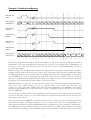
HUNT ENGINEERING
Chestnut Court, Burton Row,
Brent Knoll, Somerset, TA9 4BP, UK
Tel: (+44) (0)1278 760188,
Fax: (+44) (0)1278 760199,
Email: [email protected]
www.hunteng.co.uk
www.hunt-dsp.com
Accessing SDRAM in your FPGA Design
v 1.2 R.Williams 02-08-05
For modules in the HERON-FPGA and HERON-IO families, HUNT ENGINEERING provide a
comprehensive VHDL support package. The VHDL package consists of a “top level”, with
corresponding user constraints file, VHDL sources and simulation files for the Hardware Interface Layer,
and User VHDL files as part of many examples.
The Hardware Interface Layer correctly interfaces with the Module hardware, while the top level (top.vhd)
defines all inputs and outputs from the FPGA on your module.
Several modules provide an interface to SDRAM. There are two distinct types of SDRAM, single data rate
(called SDRAM) and Double Data Rate (Called DDR SDRAM). This means that there are two types of
Hardware Interface Layer Support.
This document discusses the capabilities of the SDRAM and DDR SDRAM interface components using
several different examples to illustrate the many ways that this component can be used.
History
Rev 1.0
First written
Rev 1.1
Added DDR SDRAM information
Rev 1.2
Added reference to 1.6Gbytes/sec DDR example
HUNT ENGINEERING is a trading style of HUNT ENGINEERING (U.K.) Ltd, Co Reg No 3333633
Directors P.Warnes & N.J.Warnes. Reg’d office 34 & 38 North St, Bridgwater, Somerset TA6 3YD. VAT Reg’d No GB 515 8449 31
SDRAM or DDR SDRAM
Before being able to use this document correctly, you need to understand which type of SDRAM you
have on your module. For example if you have a HERON-FPGA5 or HERON-FPGA7 it has Single
Data Rate SDRAM, and you need to refer to the first half of this document “SDRAM Memory”.
If you have a HERON-FPGA9 then it has Double Data Rate SDRAM and you need to refer to the
second half of this document “DDR SDRAM memory”.
This might not be an exhaustive list of modules and you need to check in the user manual for the
module that you have to determine if the memory is SDRAM or DDR SDRAM.
2
SDRAM MEMORY
The SDRAM Memory Interface Component
With modules such as the HERON-FPGA5, HUNT ENGINEERING introduced a bank of SDRAM
directly connected to the user FPGA. The SDRAM interface allows the storage of large amounts of
data. This data can be accessed in bursts at 133MHz allowing the FPGA to process that data in real
time, or to create a storage element such as a large FIFO.
Please note that in this section it is the conventional Single-Data-Rate (SDR) SDRAM memory
interface that is described. For users of modules such as the HERON-FPGA9 with Double-Data-Rate
DDR SDRAM please refer to the following section on DDR Memory.
The HE_SDRAM component of the Hardware Interface Layer presents all of the signals necessary to
read and write one bank of SDRAM memory. Issues such as SDRAM initialisation and refresh are
performed internally by the HE_SDRAM component, leaving the user free to concentrate on simply
reading and writing the memory.
The HE_SDRAM component presents two ports to the user. A read port for data to be read out of the
external SDRAM, and a write port for data to be written to the SDRAM.
The SDRAM Clock
The SDRAM interface operates at 133MHz. This frequency is obtained by using a Digital Clock
Manager (DCM) to frequency synthesize 133MHz from an input clock of 100MHz. This is
automatically done inside the HE_SDRAM component.
The generated 133MHz clock is provided as input to the USER_AP entity as the signal SDCLK. This
clock signal must be used to clock all logic that directly interfaces to the SDRAM write port and read
port.
The HE_SDRAM Write Port
The HE_SDRAM component provides a ‘write port’ that allows data to be written to the SDRAM.
SDRAM memory requires a small amount of time to open a ‘row’ of memory before a read or write
can be performed. When a row has been opened, the SDRAM can transfer one word of data on each
clock cycle.
The SDRAM is organised as 32-bit wide memory. The SDRAM interface always runs at 133MHz.
Therefore, once a row has been opened, data can be written in a burst of consecutive clock cycles at a
data rate of 532Mbytes/sec.
Before a write access can be performed to the memory, the write address must first be initialised. Once
the write address has been set up, it will automatically increment after each word is written. Therefore,
the next address initialisation is only required when a new area of memory is to be written.
The signal SDRAM_WR_ADDR(25 downto 0) must be driven with the 26-bit address for the next
write access. This value is latched by the SDRAM write interface when the address enable
SDRAM_WR_AEN is asserted (set high). The address enable must be set high for one clock cycle while
the address bus is valid, and then immediately de-asserted.
With the address initialised data can be written to the SDRAM. To begin a memory write operation, the
SDRAM_WR_READY signal must be asserted (set high) to indicate that there is data to write. When the
SDRAM interface detects the write-data-ready condition, it will open the SDRAM row indicated by the
previously initialised write address.
When the row-open process has completed data will be transferred. For each word transferred, the
3
SDRAM_WR_DONE signal will be asserted (set high) by the SDRAM interface. On each clock cycle
where the SDRAM_WR_DONE signal is asserted, valid data is expected on the write data bus,
SDRAM_WR_DATA(31 downto 0).
The signal SDRAM_WR_BURST signal should be used along with the SDRAM_WR_READY signal to
indicate that there are multiple words of data to transfer. While both signals are asserted (set high) this
indicates that the SDRAM interface can burst data to the external memory. The write burst will end if
either the end of the row is reached, or if the burst signal becomes de-asserted. If the end of row is
reached, the burst must end so that the row can be closed. If there is still more data to transfer, the next
new row will be opened when the previous has been closed.
The HE_SDRAM Read Port
The HE_SDRAM component provides a ‘read port’ that allows data to be read from the SDRAM.
SDRAM memory requires a small amount of time to open a ‘row’ of memory before a read or write
can be performed. When a row has been opened, the SDRAM can transfer one word of data on each
clock cycle.
The SDRAM is organised as 32-bit wide memory. The SDRAM interface always runs at 133MHz.
Therefore, once a row has been opened, data can be written in a burst of consecutive clock cycles at a
data rate of 532Mbytes/sec.
Before a read access can be performed to the memory, the read address must first be initialised. Once
the read address has been set up, it will automatically increment after each word is written. Therefore,
the next address initialisation is only required when a new area of memory is to be read.
The signal SDRAM_RD_ADDR(25 downto 0) must be driven with the 26-bit address for the next
read access. This value is latched by the SDRAM read interface when the address enable
SDRAM_RD_AEN is asserted (set high). The address enable must be set high for one clock cycle while
the address bus is valid, and then immediately de-asserted.
With the address initialised data can be read from the SDRAM. To begin a memory read operation, the
SDRAM_RD_READY signal must be asserted (set high) to indicate that there is space to receive data.
When the SDRAM interface detects the read-data-ready condition, it will open the SDRAM row
indicated by the previously initialised read address.
When the row-open process has completed data will be transferred. Unlike the write interface however,
the SDRAM_RD_DONE signal does not directly indicate that a data word is being output. This is because
the external SDRAM memory has a data access delay of several clock cycles. For each assertion of
SDRAM_RD_DONE this indicates that an item of data has been requested from the memory.
For each word actually transferred, the SDRAM_RD_DVAL signal will be asserted (set high) by the
SDRAM interface. On each clock cycle where the SDRAM_RD_DVAL signal is asserted, valid data is
presented on the read data bus, SDRAM_RD_DATA(31 downto 0).
The signal SDRAM_RD_BURST signal should be used along with the SDRAM_RD_READY signal to
indicate that there are multiple words of data to be read. While both signals are asserted (set high) this
indicates that the SDRAM interface can accept a burst of data from the external memory. The read
burst will end if either the end of the row is reached, or if the burst signal becomes de-asserted. If the
end of row is reached, the burst must end so that the row can be closed. If there is still more data to
transfer, the next new row will be opened when the previous has been closed.
4
Overlapping Read and Write Transfers
Although the SDRAM interface presents both a read port and a write port, the actual transfer of data is
limited to one direction at any one point in time. This is due to the fact that a common data bus is used
by the SDRAM for both reading and writing the memory.
Using the read port and write port concurrently is allowed by the HE_SDRAM component however,
as the component will automatically decide whether to perform either the requested read or the write.
Once the first transfer completes, the HE_SDRAM component will then switch to perform the other.
When using the read port and write port concurrently, you should remember the following points:
1. Both the read address enable and write address enable can be asserted simultaneously.
2. Both the read ready and write ready signals can be asserted simultaneously.
3. Both the read burst and write burst signals can be asserted simultaneously.
4. During any one clock cycle only one of the SDRAM_RD_DONE or SDRAM_WR_DONE
signals will be driven high (asserted) by the SDRAM interface.
SDRAM Memory Bandwidth
The SDRAM interface operates at 133MHz, and is organised as 32-bit wide memory. The SDRAM
interface is capable of transferring one word of data on every clock cycle while a burst access is in
progress either to or from the memory. This equates to a data rate during a burst of 532
Mbytes/second.
The sustainable data rate will typically be less than this for two main reasons.
Firstly, there is an overhead for each data access as a row of memory must first be opened before the
data transfer and then closed after the data transfer. The smaller the burst of data transferred, the larger
the effect of the row open and close on the memory bandwidth.
Secondly, there is a single data bus that is shared by both memory read and memory write operations.
For applications that are reading and writing concurrently, the total available bandwidth must be shared
between the read operation and the write operation. The ratio of read bandwidth to write bandwidth
will be controlled by the users logic.
SDRAM Memory Access Examples
There are two examples presented in the remainder of this document. The first example illustrates
writing to SDRAM and the second example illustrates reading from SDRAM.
Depending on the board type you are using you will also find SDRAM access examples on the HUNT
ENGINEERING CD and web-site. These will demonstrate the key issues involved in reading and
writing the SDRAM, and will highlight how the read port and write port of the SDRAM are suited to
directly connecting to FIFOs.
By interfacing the SDRAM to data FIFOs, it becomes easy to control the flow of data through your
design and in and out of SDRAM. The way that FIFOs can be used with both the read port and write
port is discussed in the following examples.
5
Example 1: Writing to Memory
SDRAM_WR_
AEN
SDRAM_WR_
ADDR[25:0]
A0
SDRAM_WR_
READY
SDRAM_WR_
BURST
SDRAM_WR_
DONE
SDRAM_WR_
DATA[31:0]
D0
1
2
D1
3
4
5
6
7
D2
8
D3
9
10
11
In the above diagram four words are written to memory at A0, A0+1, A0+2 and A0+3. The first
operation performed is to set the write address by asserting the SDRAM_WR_AEN along with a valid
address on SDRAM_WR_ADDR. This must be done before the SDRAM_WR_READY signal indicates data
is ready to be written at that address.
With the address set, the data ready and data burst signals are both asserted to indicate data is ready for
writing, and that there is more than one word to write. At this point there will be a variable delay while
the addressed memory row is opened ready for writing. This delay will vary depending on the activity
on the SDRAM. If a read is in progress, the write must wait for that to complete. Also, if a refresh of
memory is required this will happen before the data access begins. If there is no read activity or refresh
in progress, the transfer will start after a delay of four clock cycles.
While the transfer is in progress, as shown in clock cycles 6 to 9, one word of data will be transferred
on every clock cycle while SDRAM_WR_DONE is asserted. This will continue until the burst signal
becomes de-asserted to show there is only one word left to write. At this time SDRAM_WR_DONE will
become de-asserted and the transfer stops. At this point, the memory row is closed.
The data written to the SDRAM is the data presented on the SDRAM_WR_DATA bus during the clock
cycles where SDRAM_WR_DONE is asserted. As shown in the diagram above, the values D0, D1, D2 and
D3 are written to SDRAM memory at addresses A0, A0+1, A0+2 and A0+3 respectively.
The SDRAM write port is ideally suited for connecting directly to a FIFO. The write side of the FIFO
can be filled according to the individual needs of each application. The data output of the FIFO should
be used to directly drive the SDRAM_WR_DATA bus. The almost empty flag can be used to indicate
when the burst must stop, and the empty flag can be used to indicate when there is data ready. That is,
when the almost empty flag is asserted, the SDRAM_WR_BURST signal becomes de-asserted and when
the empty flag becomes asserted, the SDRAM_WR_READY signal becomes de-asserted. Please note, the
FIFO output data must be valid at the same time the FIFO indicates not empty, and not on the clock
cycle after the FIFO read enable is asserted. In this case, the read enable can be driven directly by
SDRAM_WR_DONE.
6
Example 2: Reading from Memory
SDRAM_RD_
AEN
SDRAM_RD_
ADDR[25:0]
A0
SDRAM_RD_
READY
SDRAM_RD_
BURST
SDRAM_RD_
DONE
SDRAM_RD_
DVAL
SDRAM_RD_
DATA[31:0]
D0
1
2
3..5
6
7
8
9
10
11
D1
12
D2
13
In the above diagram three words are read from memory at A0, A0+1 and A0+2. The first operation
performed is to set the read address by asserting the SDRAM_RD_AEN along with a valid address on
SDRAM_RD_ADDR. This must be done before the SDRAM_RD_READY signal indicates data is ready to
be read at that address.
With the address set, the data ready and data burst signals are both asserted to indicate data is ready for
reading, and that there is more than one word to read. At this point there will be a variable delay while
the addressed memory row is opened ready for reading. This delay will vary depending on the activity
on the SDRAM. If a write is in progress, the read must wait for that to complete. Also, if a refresh of
memory is required this will happen before the data access begins. If there is no write activity or refresh
in progress, the transfer will start after a delay of four clock cycles.
While the transfer is in progress, as shown in clock cycles 6 to 8, one word of data will be requested on
every clock cycle while SDRAM_RD_DONE is asserted. Please note, unlike the write port, the
SDRAM_RD_DONE signal only indicates the read has been performed to the SDRAM. The actually
transfer of data happens five clock cycles later as there is a pipeline delay for the data to be accessed
from the SDRAM.
The transfer will continue until the burst signal becomes de-asserted to show there is only one word left
to read. At this time SDRAM_RD_DONE will become de-asserted and the transfer stops. At this point,
the memory row is closed.
The data read from the SDRAM is the data presented on the SDRAM_RD_DATA bus during the clock
cycles where the data valid signal SDRAM_RD_DVAL is asserted. As shown in the diagram above, the
values D0, D1 and D2 are read from SDRAM memory at addresses A0, A0+1 and A0+2 respectively.
The SDRAM read port is ideally suited for connecting directly to a FIFO. The read side of the FIFO
can be emptied according to the individual needs of each application. The data input of the FIFO
7
should be directly driven by the SDRAM_RD_DATA bus. The almost full flag can be used to indicate
when the burst must stop, and the full flag can be used to indicate when there is no space to read. That
is, when the almost full flag is asserted, the SDRAM_RD_BURST signal becomes de-asserted and when
the full flag becomes asserted, the SDRAM_RD_READY signal becomes de-asserted.
Please note however, for the FIFO used to interface to the SDRAM read port, the almost full condition
of the FIFO must be set when there are at least 6 words of storage left. This is because with the almost
full condition driving the SDRAM_RD_BURST signal, the SDRAM_RD_DONE signal is immediately
affected, but the SDRAM_RD_DVAL signal will still be asserted from a data read five cycles ago.
Therefore, six more words will be output, rather than just one more word.
The FIFO write enable can then be directly driven by the signal SDRAM_RD_DVAL.
8
DDR SDRAM MEMORY
The DDR Memory Interface Component
With modules such as the HERON-FPGA9, HUNT ENGINEERING introduced a bank of DoubleData-Rate (DDR) SDRAM directly connected to the user FPGA. The DDR memory interface allows
the storage of large amounts of data, at higher speeds than conventional Single-Data-Rate (SDR)
SDRAM. This data can be accessed in bursts of data on both rising and falling clock edges at 200MHz
allowing the FPGA to process that data in real time, or to create a storage element such as a large
FIFO.
Please note that in this section it is the Double Data Rate SDRAM memory interface that is described.
For users of modules such as the HERON-FPGA5 with conventional SDRAM please refer to the
previous section on SDRAM Memory.
The HE_DDR component of the Hardware Interface Layer presents all of the signals necessary to read
and write one or two banks of DDR memory. Issues such as DDR initialisation and refresh are
performed internally by the HE_DDR component, leaving the user free to concentrate on simply
reading and writing the memory.
The HE_DDR component presents either two or four ports to the user. For modules with one bank of
memory, there is a read port for data to be read out of the external DDR, and a write port for data to
be written to the DDR memory. For modules with two banks of memory, there are two read ports and
two write ports.
The DDR Clock
The DDR interface operates at 200MHz. This frequency is obtained directly from a free running
200MHz clock source fed into the FPGA. The 200MHz clock source is input to a DCM that generates
the necessary internal and external clock signals for DDR operation.
The DDR read interface and DDR write interface are managed using FIFO components internal to the
HE_DDR component. These FIFOs are asynchronous, in that within the HE_DDR internal logic data
is read and written at 200MHz. On the user side of these FIFOs data is transferred in a clock domain
created by the user logic.
For a module with two separate banks of DDR memory, the signal DDR_A_USER_CLK must be
correctly driven by the user in order to use the read FIFO and write FIFO of DDR Bank A. The signal
DDR_B_USER_CLK must be correctly driven by the user in order to use to the read FIFO and write
FIFO of DDR Bank B.
The DDR Write Port
The HE_DDR component provides a ‘write port’ that allows data to be written to the DDR memory.
DDR memory is designed for high burst performance by using rising edge and falling edge data. This is
called ‘double-data-rate’ (DDR) transfer.
For one clock cycle of the memory, one word of data is transferred on the rising clock edge, and one
word is transferred on the falling edge. The result is two words every clock cycle. DDR memory
requires a small amount of time to open a ‘row’ of memory before a read or write can be performed,
but when the row has been opened data can be transferred at a very high rate.
Due to the nature of DDR memory, data needs to be written in bursts to make the best use of the
available bandwidth. The write port therefore requires data is written to the memory in groups of four
32-bit words to ensure bursting is efficient.
9
The DDR Write Port FIFOs
Data is written to the DDR memory through FIFO components internal to the HE_DDR component.
The memory write interface that is presented to the USER_AP entity therefore appears as a FIFO
interface through which all memory write operations are performed.
To perform one write access to the DDR memory, four words of data must be written to the write
interface, along with one word that defines the starting address for the burst, and two bytes of data
mask information. All of this is done through the use of four separate write interface FIFOs.
The DDR write interface is organised as a rising-edge data FIFO, a falling edge data FIFO, an address
FIFO and a data mask FIFO. The data words written to the rising edge FIFO and falling edge FIFO
are 32-bits wide. The data written to the address FIFO is 25-bits wide and the data written to the data
mask FIFO is 8-bits wide.
When transferring data words ‘data-0’, ‘data-1’, ‘data-2’ and ‘data-3’ to memory each of these FIFOs
would be written as follows:
Data word 0 is written to the write port rising edge FIFO
Data word 1 is written to the write port falling edge FIFO
Data mask is written for data word 0 and data word 1 to the data mask FIFO
Data word 2 is written to the next location of write port rising edge FIFO
Data word 3 is written to the next location of write port falling edge FIFO
Data mask is written for data word 2 and data word 3 to the data mask FIFO
An address word is written to the write port address FIFO
As data must always be written in blocks of four words, a Data Mask function has been provided. The
Data Mask function allows individuals bytes to be explicitly enabled or disabled in the data sent to the
DDR memory. For any byte that whose Data Mask bit is disabled, no data will be written to the
memory at that location. This allows blocks of data smaller than four words to be written to the DDR
memory interface.
Conversely, where bursting of larger amounts of data is required, this is simply done by keeping the
write data FIFOs full with corresponding addresses that fall within the same row.
That is, if there are several blocks of four that can be written at addresses within the same row, the
DDR interface will continue to transfer to the opened row as long as valid data exists in the rising and
falling write data FIFOs.
As each address word is read from the write address FIFO it is compared to the currently open row. If
the top 15-bits of the next address exactly match the currently open row, then the next block of four
data words will be transferred immediately to the already open memory.
In this way by ensuring a consecutive set of addresses are used in the values written to the address
FIFO, bursts much larger than four words can be created to the external DDR memory.
10
The DDR Write Port FIFO Signals
For the rising edge, falling edge, address and data mask write FIFOs, one FIFO clock signal is required.
This signal is also used for the read interface. For DDR Memory Bank A, the signal is named
DDR_A_USER_CLK. For DDR Memory Bank B, the signal is named DDR_B_USER_CLK.
This clock signal must be sourced inside the USER_AP part of the design hierarchy. The resulting
clock signal presented to the HE_DDR component is connected to the write clock input of all four
write interface FIFOs.
All logic that directly interfaces to the FIFOs must be clocked with the same clock signal driven out to
the HE_DDR component.
For the following section, all signal names given will be for the first bank of DDR memory. All DDR
Memory Bank A signals begin ‘DDR_A_’. For interfacing to DDR Memory Bank B, simply rename the
signal to start ‘DDR_B_’.
The write address FIFO is 25-bits wide. Data for the write address FIFO must be driven on the bus
DDR_A_WR_ADDR(24 downto 0). To write one address value to the write address FIFO the signal
DDR_A_WR_ADDR_WEN must be asserted (set high) for one clock cycle. The DDR_A_WR_ADDR bus
must be valid in the clock cycle where DDR_A_WR_ADDR_WEN is asserted.
The write address FIFO provides two flags to indicate whether a write can proceed. The signal
DDR_A_WR_ADDR_FF is the full flag for the write address FIFO. When this signal is asserted (set high)
the write address FIFO is full and any further writes will be ignored. The signal DDR_A_WR_ADDR_AF
is the almost full flag. When this signal is asserted (set high) the write address FIFO is almost full. Only
one more write can be completed while the FIFO is almost full.
The write rising data FIFO is 32-bits wide. Data for the rising data FIFO must be driven on the bus
DDR_A_WR_DATA(39 downto 8). Please note, the DDR_A_WR_DATA bus is shared for accesses to
the rising data FIFO, the falling data FIFO and the data mask FIFO. Ensure you use the correct
portion of this bus according to the FIFO you are updating.
To write one word to the rising data FIFO the signal DDR_A_WR_RISE_WEN must be asserted (set
high) for one clock cycle. The DDR_A_WR_DATA(39 downto 8) bus must be valid in the clock cycle
where DDR_A_WR_RISE_WEN is asserted.
The rising data FIFO provides two flags to indicate whether a write can proceed. The signal
DDR_A_WR_RISE_FF is the full flag for the rising data FIFO. When this signal is asserted (set high)
the rising data FIFO is full and any further writes will be ignored. The signal DDR_A_WR_RISE_AF is
the almost full flag. When this signal is asserted (set high) the rising data FIFO is almost full. Only one
more write can be completed while the FIFO is almost full.
The write falling data FIFO is 32-bits wide. Data for the falling data FIFO must be driven on the bus
DDR_A_WR_DATA(71 downto 40). Please note, the DDR_A_WR_DATA bus is shared for accesses to
the rising data FIFO, the falling data FIFO and the data mask FIFO. Ensure you use the correct
portion of this bus according to the FIFO you are updating.
To write one word to the falling data FIFO the signal DDR_A_WR_FALL_WEN must be asserted (set
high) for one clock cycle. The DDR_A_WR_DATA(71 downto 40) bus must be valid in the clock
cycle where DDR_A_WR_FALL_WEN is asserted.
The falling data FIFO provides two flags to indicate whether a write can proceed. The signal
DDR_A_WR_FALL_FF is the full flag for the falling data FIFO. When this signal is asserted (set high)
the falling data FIFO is full and any further writes will be ignored. The signal DDR_A_WR_FALL_AF is
the almost full flag. When this signal is asserted (set high) the falling data FIFO is almost full. Only one
more write can be completed while the FIFO is almost full.
The write data mask FIFO is 8-bits wide. Data for the data mask FIFO must be driven on the bus
DDR_A_WR_DATA(7 downto 0). Please note, the DDR_A_WR_DATA bus is shared for accesses to
11
the rising data FIFO, the falling data FIFO and the data mask FIFO. Ensure you use the correct
portion of this bus according to the FIFO you are updating.
To write one byte to the data mask FIFO the signal DDR_A_WR_DM_WEN must be asserted (set high)
for one clock cycle. The DDR_A_WR_DATA(7 downto 0) bus must be valid in the clock cycle where
DDR_A_WR_DM_WEN is asserted.
The data mask FIFO provides two flags to indicate whether a write can proceed. The signal
DDR_A_WR_DM_FF is the full flag for the data mask FIFO. When this signal is asserted (set high) the
data mask FIFO is full and any further writes will be ignored. The signal DDR_A_WR_DM_AF is the
almost full flag. When this signal is asserted (set high) the data mask FIFO is almost full. Only one
more write can be completed while the FIFO is almost full.
Each bit of the byte value written to the data mask FIFO corresponds to an enable for one byte lane of
data. If the corresponding bit is set low, the data byte is written to memory (enabled) and if the
corresponding bit is set high, the data byte is not written (disabled). The bits in the data mask are
defined as follows:
Bit 0
Bit 1
Bit 2
Bit 3
Bit 4
Bit 5
Bit 6
Bit 7
Byte 0 of falling data
Byte 1 of falling data
Byte 2 of falling data
Byte 3 of falling data
Byte 0 of rising data
Byte 1 of rising data
Byte 2 of rising data
Byte 3 of rising data
12
The DDR Read Port
The HE_DDR component provides a ‘read port’ that allows data to be read from the DDR memory.
DDR memory is designed for high burst performance by using rising edge and falling edge data. This is
called ‘double-data-rate’ (DDR) transfer.
For one clock cycle of the memory, one word of data is transferred on the rising clock edge, and one
word is transferred on the falling edge. The result is two words every clock cycle. DDR memory
requires a small amount of time to open a ‘row’ of memory before a read or write can be performed,
but when the row has been opened data can be transferred at a very high rate.
Due to the nature of DDR memory, data needs to be read in bursts to make the best use of the
available bandwidth. The read port therefore requires data is read from memory in groups of four 32bit words to ensure bursting is efficient.
The DDR Read Port FIFOs
Data is read from the DDR memory through FIFO components internal to the HE_DDR component.
The memory read interface that is presented to the USER_AP entity therefore appears as a FIFO
interface through which all memory read operations are performed.
To perform one read access from the DDR memory, one word must be written to define the starting
address for the burst. Once the access from memory has been completed four words of data will be
presented to the read interface. All of this is done through the use of three separate read interface
FIFOs.
The DDR read interface is organised as a rising-edge data FIFO, a falling edge data FIFO and an
address FIFO. The data words read from the rising edge FIFO and falling edge FIFO are 32-bits wide.
The data written to the address FIFO is 25-bits wide.
When transferring data words ‘data-0’, ‘data-1’, ‘data-2’ and ‘data-3’ from memory each of these FIFOs
would be used as follows:
An address word is written to the read port address FIFO
…when the access to memory has completed…
Data word 0 is read from the read port rising edge FIFO
Data word 1 is read from the read port falling edge FIFO
Data word 2 is read from the read port rising edge FIFO
Data word 3 is read from the read port falling edge FIFO
As data must always be read in blocks of four words this may mean more words of data are read than
were required. Unlike the write port, no data mask function is provided. Instead, words of data that are
read but not required must simply be discarded by the logic that reads from the read rising data FIFO
and read falling data FIFO. This will allow blocks of data smaller than four words to be read from the
DDR memory interface.
Conversely, where bursting of larger amounts of data is required, this is simply done by keeping the
read data FIFOs empty and providing multiple addresses that fall within the same row.
That is, if there are several blocks of four that need to be read from addresses within the same row, the
DDR interface will continue to transfer from the opened row as long as there is space in the rising and
falling read data FIFOs and appropriate addresses exist in the address FIFO.
As each address word is read from the read address FIFO it is compared to the currently open row. If
the top 15-bits of the next address exactly match the currently open row, then the next block of four
data words will be transferred immediately from the already open memory.
In this way by ensuring a consecutive set of addresses are used in the values written to the address
13
FIFO, bursts much larger than four words can be created from the external DDR memory.
The DDR Read Port FIFO Signals
For the rising edge, falling edge and address FIFOs, one FIFO clock signal is required. This signal is
also used for the write interface. For DDR Memory Bank A, the signal is named DDR_A_USER_CLK.
For DDR Memory Bank B, the signal is named DDR_B_USER_CLK.
This clock signal must be sourced inside the USER_AP part of the design hierarchy. The resulting
clock signal presented to the HE_DDR component is connected to the clock inputs of all three read
interface FIFOs.
All logic that directly interfaces to the FIFOs must be clocked with the same clock signal driven out to
the HE_DDR component.
For the following section, all signal names given will be for the first bank of DDR memory. All DDR
Memory Bank A signals begin ‘DDR_A_’. For interfacing to DDR Memory Bank B, simply rename the
signal to start ‘DDR_B_’.
The read address FIFO is 25-bits wide. Data for the read address FIFO must be driven on the bus
DDR_A_RD_ADDR(24 downto 0). To write one address value to the read address FIFO the signal
DDR_A_RD_ADDR_WEN must be asserted (set high) for one clock cycle. The DDR_A_RD_ADDR bus
must be valid in the clock cycle where DDR_A_RD_ADDR_WEN is asserted.
The read address FIFO provides two flags to indicate whether a write can proceed. The signal
DDR_A_RD_ADDR_FF is the full flag for the read address FIFO. When this signal is asserted (set high)
the read address FIFO is full and any further writes will be ignored. The signal DDR_A_RD_ADDR_AF
is the almost full flag. When this signal is asserted (set high) the read address FIFO is almost full. Only
one more write can be completed while the FIFO is almost full.
The read rising data FIFO is 32-bits wide. Data from the rising data FIFO must be read on the bus
DDR_A_RD_DATA(31 downto 0). Please note, the DDR_A_RD_DATA bus is shared for accesses
from the rising data FIFO and the falling data FIFO. Ensure you use the correct portion of this bus
according to the FIFO you are reading.
To read one word from the rising data FIFO the signal DDR_A_RD_RISE_REN must be asserted (set
high) for one clock cycle. The DDR_A_RD_DATA(31 downto 0) bus will become valid in the
following clock cycle from where DDR_A_RD_RISE_REN was asserted.
The rising data FIFO provides two flags to indicate whether a read can proceed. The signal
DDR_A_RD_RISE_EF is the empty flag for the rising data FIFO. When this signal is asserted (set high)
the rising data FIFO is empty and any further reads will be ignored. The signal DDR_A_RD_RISE_AE
is the almost empty flag. When this signal is asserted (set high) the rising data FIFO is almost empty.
Only one more read can be completed while the FIFO is almost empty.
The read falling data FIFO is 32-bits wide. Data from the falling data FIFO must be read on the bus
DDR_A_RD_DATA(63 downto 32). Please note, the DDR_A_RD_DATA bus is shared for accesses
from the rising data FIFO and the falling data FIFO. Ensure you use the correct portion of this bus
according to the FIFO you are reading.
To read one word from the falling data FIFO the signal DDR_A_RD_FALL_REN must be asserted (set
high) for one clock cycle. The DDR_A_RD_DATA(63 downto 32) bus will become valid in the
following clock cycle from where DDR_A_RD_FALL_REN was asserted.
The falling data FIFO provides two flags to indicate whether a read can proceed. The signal
DDR_A_RD_FALL_EF is the empty flag for the falling data FIFO. When this signal is asserted (set
high) the falling data FIFO is empty and any further reads will be ignored. The signal
DDR_A_RD_FALL_AE is the almost empty flag. When this signal is asserted (set high) the falling data
FIFO is almost empty. Only one more read can be completed while the FIFO is almost empty.
14
The DDR Data Count
At any one point in time, the internal logic of the HE_DDR component can only be performing either
a read or a write, if the DDR memory interface is active.
The user logic however is free to update the write interface FIFOs and read interface FIFOs at the
same time. The internal logic of the HE_DDR component must therefore decide based on this activity
whether to perform a read or a write.
As the FIFOs decouple read and write activity between the USER_AP logic and the HE_DDR internal
logic it is not always obvious from the USER_AP side of the FIFOs whether a write of data has
completed. Sometimes the data to be written may still be waiting inside the rising data and falling data
write FIFOs as a different DDR access is currently underway.
There are design situations where it is necessary to know how much data has been read or written
inside the HE_DDR component. A simple example of such a situation where this is important is where
the DDR memory interface is being used to create a large FIFO.
When creating a FIFO using DDR memory, logic in the USER_AP part of the design must keep track
of how many items are in the FIFO, or rather, how many words of data have been stored in DDR
SDRAM.
For example, if 8 words are written to the write interface FIFOs, the USER_AP logic might wish to
record that the ‘DDR FIFO’ now contains 8 items. So if this is done, the read side of DDR FIFO will
now think it correct to allow a read from memory of up to 8 words. While the 8 words are still in the
write interface FIFOs and not in external memory this is incorrect.
In order to avoid this situation the HE_DDR component provides a data count bus named
DDR_A_DATA_COUNT(31 downto 0) for Bank A and a bus named DDR_B_DATA_COUNT(31
downto 0) for Bank B. For each data count there is a count reset signal. For Bank A this signal is
DDR_A_USER_RST and for Bank B this signal is DDR_B_USER_RST.
The reset signal is used to set the count value to zero. This reset signal is asynchronous, but to ensure
correct operation it should be asserted for at least 10ns.
The data count logic records the number of accesses made to the DDR memory. For each group of
four words written to memory (one write access) the data count increments by one, and for each group
of four words read from memory (one read access) the data count decrements by one. The counter is
32-bits in size and will roll around when counting up from all bits set, and will roll when counting
down from zero.
An example of the use of the data count function can be seen in the SDRAM_FIFO example provided
for all boards that have a DDR interface.
15
Overlapping DDR Read and Write Transfers
Although the DDR interface presents both a read port and a write port, the actual transfer of data to or
from the external DDR memory is limited to one direction at any one point in time. This is due to the
fact that a common data bus is used by the DDR memory for both reading and writing.
Using the read port and write port concurrently is allowed by the HE_DDR component however as
the interfaces are presented as FIFOs for read data and FIFOs for write data. The logic created in the
USER_AP entity is completely free to access both sets of FIFOs at the same time.
Inside the HE_DDR component, the internal logic will automatically decide whether to perform a read
or write access according to the current state of the interface FIFOs and the DDR memory.
When both the read interface FIFOs and write interface FIFOs are ready to proceed for a read or write
memory access the internal logic of the DDR component will alternate equally between read and write.
Users should note that if a read access follows a write access, or if a write access follows a read access,
and the row addresses are different, that this will create the need for the current row to be closed and
the new row to be opened. Users who wish to control the arbitration of read versus write should do so
within the USER_AP entity by controlling when the read and write interface FIFOs are set.
DDR Memory Bandwidth
One bank of DDR memory interface operates at 200MHz, and is organised as 32-bit wide memory.
The DDR interface is capable of transferring two words of data on every clock cycle while a burst
access is in progress either to or from the memory. For each memory cycle data is transferred on both
the rising edge and the falling edge.
This equates to a data rate during a burst of 1.6 Gbytes/second for one Bank of DDR memory, or 3.2
Gbytes/second where two Banks of DDR memory are used in parallel. The sustainable data rate will
typically be less than this for two main reasons.
Firstly, there is an overhead for each data access as a row of memory must first be opened before the
data transfer and then closed after the data transfer. The smaller the burst of data transferred, the larger
the effect of the row open and close on the memory bandwidth.
Secondly, there is a single data bus that is shared by both memory read and memory write operations.
For applications that are reading and writing concurrently, the total available bandwidth must be shared
between the read operation and the write operation. The ratio of read bandwidth to write bandwidth
will be controlled by the users logic.
DDR Memory Access Examples
There are three examples presented in the remainder of this document. The first example illustrates
writing to DDR memory, the second example illustrates reading from DDR memory, and the third
example illustrates use of the write data mask function.
Depending on the board type you are using you will also find DDR access examples on the HUNT
ENGINEERING CD and web-site. These will demonstrate the key issues involved in reading and
writing DDR memory, and will highlight how the read interface FIFOs and write interface FIFOs are
suited to accessing DDR SDRAM.
By interfacing to DDR SDRAM through FIFOs, it becomes easy to control the flow of data through
your design and in and out of memory. The way that the FIFO interfaces should be used for both
reading and writing memory is discussed in the following examples.
In particular, there is an example of how to write logic to access the DDR memory at the full rate of
1.6Gbytes/sec. This example logic is part of the SDRAM FIFO Example (Example 3) which can be
found on the HUNT ENGINEERING CD and web-site.
16
Example 1: Writing to Memory
DDR_A_WR
_RISE_WEN
DDR_A_WR
_DATA[39:8]
D2
D0
D4
D6
DDR_A_WR
_FALL_WEN
DDR_A_WR
DATA[71:40]
D1
D3
D5
D7
M01
M23
M45
M67
DDR_A_WR
_DM_WEN
DDR_A_WR
_DATA[7:0]
DDR_A_WR
ADDR_WEN
DDR_A_WR
ADDR[24:0]
A0
1
2
3
4
A4
5
6
7
8
9
10
11
In the above diagram eight words are written to memory at A0 to A7. There are four FIFOs involved
in this operation. The rising data FIFO, the falling data FIFO, the data mask FIFO and the address
FIFO. It is assumed that all FIFO flags are checked such that no time are any of the FIFOs full. This is
done using the FIFO flags presented by the DDR memory interface component.
The diagram shows words written alternately to first the rising edge write FIFO and then the falling
edge write FIFO. It is not necessary for theses accesses to be performed on every other cycle, as it is
valid to write to both the rising and falling data FIFOs on every clock cycle. It has been shown this way
to represent the situation where the data source for the memory write is a 32-bit wide stream such as a
32-bit wide FIFO. In this situation only one word can possibly be read at a time from the data source,
so accesses would be alternated to first the rising edge FIFO and then the falling edge FIFO.
Alternatively, if the data source inside the FPGA were 64-bits wide then data could be streamed into
both rising and falling data FIFOs at the same time.
For each word written to the address FIFO using DDR_A_WR_ADDR_WEN, two words each must have
been written to the rising edge FIFO, the falling edge FIFO and the data mask FIFO. One word of
data in the address FIFO will be used to begin a single write access to the DDR memory. One write
access is always done with four words of data taken alternately from the rising data FIFO and then the
falling data FIFO. For each word pair taken from the data FIFOs, one byte of data will be read from
the data mask FIFO in order to know which bytes to enable onto the memory.
17
As the HE_DDR component begins writing a four word burst to memory, the next address is fetched
from the address FIFO and compared to the address of the currently opened row.
If the address matches such that the top 15 bits of the 25-bit address is the same then the next access
will be within the currently open row. In this situation the four word burst of the current access is
immediately followed by a four word burst for the next access.
In this way data can be streamed into the DDR memory at the rate of two words every 200MHz clock
cycle, for several cycles. This gives a write burst rate of 1.6Gbytes/sec to one bank of DDR memory.
When an address is fetched that has a different row address according to the top 15 bits, then the next
row will require a different row to be opened. This process will introduce some delay to operation
while the current row is closed and the new row is opened.
If during a write access to memory both the write interface FIFOs and read interface FIFOs remain
empty, then the memory row will automatically be closed when the current write completes.
18
Example 2: Reading from Memory
DDR_A_RD_
ADDR_WEN
DDR_A_RD_
ADDR[24:0]
A0
A4
DDR_A_RD_
RISE_EF
DDR_A_RD_
RISE_REN
DDR_A_RD_
FALL_EF
DDR_A_RD_
FALL_REN
DDR_A_RD_
DATA[31:0]
D0
D2
DDR_A_RD_
DATA[63:32]
D4
D1
1
2
3
4
5
6
7
D3
8
9
D5
10
11
In the above diagram eight words are read from memory at A0 to A7. There are three FIFOs involved
in this operation, the rising data FIFO, the falling data FIFO and the address FIFO. It is assumed that
the address FIFO flags are checked such that no time is the address FIFO full. This is done using the
FIFO flags presented by the DDR memory interface component.
The diagram shows words read alternately from first the rising edge read FIFO and then the falling
edge read FIFO. It is not necessary for theses accesses to be performed on every other cycle, as it is
valid to read both the rising and falling data FIFOs on every clock cycle. It has been shown this way to
represent the situation where the data destination for the memory read is a 32-bit wide stream such as a
32-bit wide FIFO. In this situation only one word can possibly be written at a time to the data
destination, so accesses would be alternated to first the rising edge FIFO and then the falling edge
FIFO.
Alternatively, if the destination inside the FPGA were 64-bits wide then data could be streamed from
both rising and falling data FIFOs at the same time.
For each word written to the address FIFO using DDR_A_RD_ADDR_WEN, four words will be read
from DDR memory. These words will arrive as two words in the rising edge FIFO interlaced with two
words in the falling edge FIFO.
It should be noted that there will always be some time delay between the read address FIFO being
written and the data arriving in the read data FIFOs. This is indicated by the break in signal timing
shown between clock cycle 3 and clock cycle 4 in the diagram above. The best case for read latency is
where the DDR memory interface is currently inactive when the write to the read address FIFO is
19
performed. As soon as the HE_DDR component detects the address, the read access will begin a short
time later data will appear in the read data FIFOs.
Alternatively, another access such as a memory write or memory refresh may be in progress when the
read address FIFO is updated. In this situation the current access will first be completed and then the
read started.
As the HE_DDR component begins reading a four word burst from memory, the next address is
fetched from the address FIFO and compared to the address of the currently opened row.
If the address matches such that the top 15 bits of the 25-bit address is the same then the next access
will be within the currently open row. In this situation the four word burst of the current access is
immediately followed by a four word burst for the next access.
In this way data can be streamed from the DDR memory at the rate of two words every 200MHz clock
cycle, for several cycles. This gives a read burst rate of 1.6Gbytes/sec from one bank of DDR memory.
When an address is fetched that has a different row address according to the top 15 bits, then the next
row will require a different row to be opened. This process will introduce some delay to operation
while the current row is closed and the new row is opened.
If during a read access from memory both the write interface FIFOs and read interface FIFOs remain
empty, then the memory row will automatically be closed when the current read completes.
20
Example 3: Using the Write Data Mask Function
DDR_A_WR
_RISE_WEN
DDR_A_WR
_DATA[39:8]
D0
DDR_A_WR
_FALL_WEN
DDR_A_WR
DATA[71:40]
DDR_A_WR
_DM_WEN
DDR_A_WR
_DATA[7:0]
M0
M1
DDR_A_WR
ADDR_WEN
DDR_A_WR
ADDR[24:0]
A0
1
2
3
4
5
6
7
8
9
10
11
The data mask function is necessary when trying to write to less than four locations of memory. For
normal operation, data would always be written in groups of four words as this allows the DDR
memory interface to burst at the most efficient rate. This section describes a situation where only word
is to be written to memory.
In the above diagram one word is written to memory at address A0. It is assumed that all FIFO flags
are checked such that no time are any of the FIFOs full. This is done using the FIFO flags presented
by the DDR memory interface component.
The diagram shows words written alternately to first the rising edge write FIFO and then the falling
edge write FIFO. Please note that it is very important to complete all four writes to the data FIFOs to
ensure that the word values that are to be written are in the correct position within the sequence of
four.
In the diagram there is only one word of valid data presented for the first access to the rising data
FIFO. All four write accesses are performed though and dummy data values are provided for the last
three accesses of the burst. These last three word values will not be written to memory if the data mask
values are set appropriately.
For each pair of words written to the rising data FIFO and falling data FIFO, one byte must be written
to the data mask FIFO. This must always be done, regardless of whether the data mask function is
being used. For normal operation where all words of the burst are to be written, the byte value written
to the data mask FIFO must be zero to enable all bytes of all words.
Each bit of the byte value written to the data mask FIFO corresponds to an enable for one byte lane of
21
data. If the corresponding bit is set low, the data byte is written to memory (enabled) and if the
corresponding bit is set high, the data byte is not written (disabled). The bits in the data mask are
defined as follows:
Bit 0
Bit 1
Bit 2
Bit 3
Bit 4
Bit 5
Bit 6
Bit 7
Byte 0 of falling data
Byte 1 of falling data
Byte 2 of falling data
Byte 3 of falling data
Byte 0 of rising data
Byte 1 of rising data
Byte 2 of rising data
Byte 3 of rising data
So for our example in the diagram above, only the first word of the four words in the burst are to be
written. Therefore the value of the byte M0 in the diagram would be 0Fh. This would enable all bytes
of the rising data word D0 that is written with the first assertion of DDR_A_WR_RISE_WEN. All bytes
of the falling data would be disabled for the first assertion of DDR_A_WR_FALL_WEN.
The value of the byte M1 in the diagram would be FFh. This would disable all bytes for the data written
by the second assertion of the signal DDR_A_WR_RISE_WEN and the second assertion of the signal
DDR_A_WR_FALL_WEN.
22