1
Example 2: Reading from Memory
SDRAM_RD_
AEN
SDRAM_RD_
ADDR[25:0]
A0
SDRAM_RD_
READY
SDRAM_RD_
BURST
SDRAM_RD_
DONE
SDRAM_RD_
DVAL
SDRAM_RD_
DATA[31:0]
D0
1
2
3..5
6
7
8
9
10
11
D1
12
D2
13
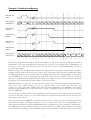
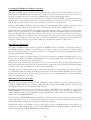
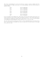
In the above diagram three words are read from memory at A0, A0+1 and A0+2. The first operation
performed is to set the read address by asserting the SDRAM_RD_AEN along with a valid address on
SDRAM_RD_ADDR. This must be done before the SDRAM_RD_READY signal indicates data is ready to
be read at that address.
With the address set, the data ready and data burst signals are both asserted to indicate data is ready for
reading, and that there is more than one word to read. At this point there will be a variable delay while
the addressed memory row is opened ready for reading. This delay will vary depending on the activity
on the SDRAM. If a write is in progress, the read must wait for that to complete. Also, if a refresh of
memory is required this will happen before the data access begins. If there is no write activity or refresh
in progress, the transfer will start after a delay of four clock cycles.
While the transfer is in progress, as shown in clock cycles 6 to 8, one word of data will be requested on
every clock cycle while SDRAM_RD_DONE is asserted. Please note, unlike the write port, the
SDRAM_RD_DONE signal only indicates the read has been performed to the SDRAM. The actually
transfer of data happens five clock cycles later as there is a pipeline delay for the data to be accessed
from the SDRAM.
The transfer will continue until the burst signal becomes de-asserted to show there is only one word left
to read. At this time SDRAM_RD_DONE will become de-asserted and the transfer stops. At this point,
the memory row is closed.
The data read from the SDRAM is the data presented on the SDRAM_RD_DATA bus during the clock
cycles where the data valid signal SDRAM_RD_DVAL is asserted. As shown in the diagram above, the
values D0, D1 and D2 are read from SDRAM memory at addresses A0, A0+1 and A0+2 respectively.
The SDRAM read port is ideally suited for connecting directly to a FIFO. The read side of the FIFO
can be emptied according to the individual needs of each application. The data input of the FIFO
7