1
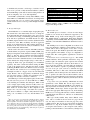
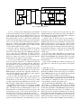
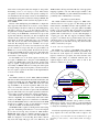
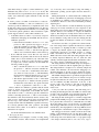
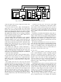
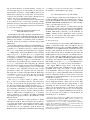
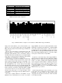
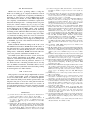
An FPGA-based Multi-Core Platform for Testing
and Analysis of Architectural Techniques
Willard G. Simoneau and Resit Sendag
Department of Electrical, Computer and Biomedical Engineering
University of Rhode Island
Kingston, RI 02881
simoneau,[email protected]
Abstract—This paper covers the design and FPGA-based
prototyping of a full-featured multi-core platform for use in
computer architecture research studies. Existing platforms for
performing studies include software simulators and hardwareassisted simulators, but there are no modular full-hardware
platforms designed to measure a wide range of performance
metrics. Such a platform, using HDL synthesis onto an FPGA,
can run orders of magnitude faster than software-based solutions
at the cost of having less flexible processor configuration and
implementation. This paper presents an end-to-end solution, from
bottom-level hardware design all the way to automated results
collection and analysis, which can be used with inexpensive
commodity hardware.
I. I NTRODUCTION
In computer architecture, there is a growing need to evaluate
the performance and cost of new, complex architectural ideas.
Currently, most evaluation is done with simulations [1], [2],
[3], [9], [11], [20], but these simulators are typically quite
slow. It is difficult to get accurate results quickly. Consequently, there has been research into hardware acceleration
of these simulators using FPGAs (field-programmable gate
arrays) [7], [6], [18], [17], [8], [5], [12], [19], [16], [4],
[14]. Many of these techniques use a seperate functional
model (usually [7], [17], [14] but not always [8] softwarebased) paired with an FPGA-based timing model. FPGAaccelerated models are several orders of magnitude faster than
their software counterparts, especially when simulating multicore systems.
Current FPGA-accelerated simulation platforms have
demonstrated FPGAs as viable architecture research vehicle.
However, they fall short in terms of providing tools which are
fully open-source and easy to experiment with. For example,
HAsim[13] and FAST[7] provide valuable insight into how
FPGA-accelerated simulators can be designed, but they are not
open-source. Their utility is limited to a few research groups
in academia and industry. The difficulty in designing and
verifying an FPGA-accelerated simulator leads to a scarcity of
tools. The few existing open-source tools (e.g., RAMP Gold
[17] and ProtoFlex [8] are not straightforward to use, modify
and/or generate results with.
The end result is that FPGA-accelerated simulators have not
become popular in computer architecture research community.
More FPGA platforms are needed to popularize their use
in the research community. These systems should preferably
provide a full solution: easy to use, modify, debug and verify,
and an automated experiment setup. To address this need,
we introduce in this paper a new FPGA-based architecture
exploration platform, the Z48001 .
The Z4800 is not aimed at replacing any existing FPGAaccelerated simulation platforms: for different type of research
studies as well as educational objectives, different tools will
be appropriate. The Z4800 focuses on testing and analysis
of single-core and small-scale (2-16 core) multi-core systems
rather than large-scale systems such as those targetted by
ProtoFlex and RAMP Gold. It can run unmodified Linux-based
operating systems over network filesystems such as NFS or
from local storage such as a USB drive.
The main design philosophy of the Z4800 is centered
around ease of adaptation and use. It is supported by a fully
automatic synthesis and benchmarking system that provides
a mechanism to run a large number of experiments with no
human intervention. It also provides extensive run-time debug
and verification interfaces. Consequently, it is an end-to-end
FPGA-based platform that can be used not only for computer
architecture research, but also for operating system research
and for software debugging.
II. Z4800: A C ONFIGURABLE AND M ODULAR FPGA
C OMPUTER
The Z4800 is an open-source multi-core research platform
which can be directly synthesized for a commodity FPGA
and can run a full, unmodified Linux-based operating system.
It can be configured to run at up to 55MHz while achieving
0.7 average per-core IPC (instructions per clock cycle) using
only a $300 FPGA board. Per-core IPC of up to 0.85 can be
achieved with larger caches at the expense of FPGA resource
consumption. The design is modularized, so that individual
components can be replaced and redesigned to test new architectural ideas. The design also has extensive instrumentation; a
large number of performance counters (currently 80) are used
1 The Z4800 implements a 32-bit subset of the MIPSR4000
R
ISA. Most
MIPS implementations use R as their first letter, so we have used Z. Other
R
R
MIPS implementations include the R4000,
R4400,
and so on. We
arbitrarily pick the name Z4800 because it is capable of running code compiled
R
for R4xxx processors, including kernel code. MIPSis
a registered trademark
of MIPS Technologies, Inc., and the Z4800 is not endorsed by nor associated
with MIPS Technologies, Inc.
to simultaneously measure a wide range of statistics in realtime. It also provides a fully-automated hardware synthesis
and benchmarking system and an extensive debug interface. It
promotes simplicity, ease of use and adaptability.
The Z4800 is synthesizable on many Altera FPGAs; on the
Altera DE2-115, a $300 FPGA board based on an inexpensive
Cyclone IV-E chip, a 4-core system is quite practical. Larger
systems with 16 or more cores are possible in high-end Stratix
FPGAs.
Frontend pipeline
Decode/group logic
Backend pipeline (pipeline, ALU/mul/div, Coprocessor 0)
L1/L2 caches, cache controllers, and glue logic
Replacement Algorithms (LRU, Pseudo-LRU, Random, Hybrid)
L1 TLBs, JTLB
Debug features (not necessary for running CPU)
Performance counters
TOTAL
394
1200
1602
2304
528
855
474
60
10090
TABLE I: Number of lines of VHDL code for Z4800, including optional debug modules.
A. Design Philosophy
The Z4800 takes on a somewhat unique design philosophy.
The central idea is that functionality and ease of design are
more important than other design metrics (area, speed, power,
etc). Instead of focusing on maximizing performance per logic
block and micro-optimization, the Z4800 instead uses highlevel RTL (register-transfer level) constructs. Synthesized area
is traded for easier RTL, modularity, and more aggressive
design on an architectural level. The resulting design runs at
moderate clock rates, but it can easily be modified to study
various architectural enhancements.
Blocks such as the cache controllers and TLBs (translation
lookaside buffers) are split into seperate VHDL (VHSIC (very
high speed integrated circuit) hardware description language)
entities so that they can be rewritten and replaced independently. However, modularization does not extend much beyond this level. This is beneficial because over-modularization
would obfuscate the design; imagine trying to make sense of
a design in which every gate and flip-flop was instantiated
seperately. One must consider the human writing the HDL
as part of the design process. The time and effort of handoptimizing the HDL could be the difference between a design
that functions and one that does not; tolerating higher logic
consumption results in a bigger, slower, but still functional
design. Besides, with an appropriately modularized design,
one can always return to optimize the problematic parts of
the design once absolute correctness is achieved.
The ultimate proof of this design philosophy is in the results.
The fully functional processor is about 10K lines of VHDL
code, including all comments and whitespace. Much of that
code is simply signal routing between modules. The core’s
logic is instantiated using only a few thousand lines of code.
More details are shown in Table I. The compilation of the
design is also very fast. Using a reasonable host system, it
takes about 11 minutes to compile a fully functional system
with 1 core, 15 minutes for 2 cores, and 40 minutes for 4
cores.2 .
2 These are worst-case cold compile times including all phases (analysis,
synthesis, fitting, timing analysis) targetted for the DE2-115 board. Incremental compilation and reduced cache/TLB configurations will improve on
these compile times. The 4-core design begins pushing the limits of the FPGA,
so its compile time is much longer. If a larger FPGA is used, compilation
time can be greatly decreased since less place/route effort is required. The
host machine used here was a Dell Poweredge 1950 with a pair of quad-core
Xeon X5460 CPUs and 32GB RAM.
B. Microarchitecture
The Z4800 processor features a 2-issue in-order integer
pipeline. It can execute most instructions supported by the
MIPS R4000, except 64-bit and floating-point operations.
The Z4800 includes a full-featured TLB which maintains
compatibility with the R4000 TLB. The implemented ISA is
sufficient to run unmodified GNU/Linux distributions such as
Debian.
The Z4800 processor aims for high IPC at moderate clock
rates, and emphasizes simplicity and modularity when reasonable. This is done at the expense of area, and to a lesser
extent, clock speed. The Z4800 is superscalar with symmetric
in-order pipelines. The number of stages is configurable at
compile time. The overall pipeline organization is shown in
Figure 1.
1) Instruction Fetch and Instruction Queue: The Z4800
includes hardware which prefetches instructions along the
predicted path. An instruction queue seperates the frontend
from the rest of the pipeline and allows the frontend to run
ahead along the predicted code path while the backend is
stalled. The frontend is capable of prefetching instructions
at a rate of two per cycle, even across cacheline and page
boundaries. This serves to hide some of the Icache and ITLB
miss penalties. The frontend pre-decodes instructions and is
able to predict both taken and not-taken branches with 0
penalty cycles. Fetched instructions are written into the Iqueue
(instruction queue), which is drained by the DG (Decode and
Group) stage.
2) Speculative Exception Handling: ITLB faults are raised
speculatively on the Z4800. The decode stage rewrites instructions that have faulted the ITLB into trap instructions.
The trap instructions internally have the same opcode as the
explicit MIPS software traps, but the exception that is raised
will use the appropriate TLB exception code. If the faulting
ITLB access is a wrong-path reference, it will be annulled by
a pipeline flush and therefore it will have no architecturally
visible effects.
This logic cleanly handles many rather difficult corner
cases, such as a branch at the last word in a page. In this
case, the delay-slot instruction in the next page may cause
a TLB exception. The decode stage will rewrite the faulting
instruction to a trap in the branch’s delay-slot, resulting in
an exception raised with EPC (the exception restart address)
pointing to the branch. This is correct behavior [10, Page 121].
RR
EX
M1
RW
BP
Icache
Dcache
Iqueue
DG
Rfile
mul/div
cop0
predecode
RR
EX
M1
RW
BP
Fig. 1: Pipeline organization
3) Decode and Group (DG): The DG stage routes machine
code from the instruction queue through the instruction decoders and the grouper. Two candidate instructions are read
from the queue and decoded into pipeline control signals. If
the grouper decides it is safe to issue them in parallel, then
both are issued and the Iqueue advances by 2 words. If parallel
issue is not safe, then only the first instruction will issue to
pipe 0, pipe 1 will be issued a NOP, and the Iqueue will only
advance by 1 word. If later pipeline stages are stalled, nothing
is issued and the Iqueue does not advance.
If the first of the two instructions coming from the Iqueue
is a branch, then the second instruction is its delay slot
instruction. A rather simple approach to handling branch delay
slots is used: delay slot instructions are always issued in
parallel with the branch. If the delay slot instruction is not
present (i.e. Iqueue only contains one valid word) then the
branch will not issue until it becomes available.
4) Register Read (RR): In the RR stage, the register file is
read to provide four operands for two instructions. Operands
from later pipeline stages are muxed with the output from
the register file. If an operand is marked as invalid, then the
data has been overwritten but is not known yet; use of such
an operand will cause this stage to stall. Invalid operands are
generated by late-result instructions such as loads; this causes
RAW-dependent (read-after-write dependent) instructions to
stall. An entire pipeline stage is dedicated to this operation
to avoid it becoming the critical path.
5) Execute (EX): In the EX stage, the ALU will perform
the necessary operation. Data cache virtual addresses are
calculated here as well. This stage is the first stage at which
operands are guaranteed ready. Branches are resolved as well;
EX will trigger a pipeline flush if a branch mispredicts.
Of particular note in this stage is the support for operand
cascading. If this option is turned on, the Z4800 can issue
pairs of instructions that are RAW-dependent. A direct combinational path is provided from the ALU in pipe 0 to the
operand inputs of pipe 1. This means that the ALUs only
have half a clock cycle each to perform their operations.
It is important to note that the instruction in pipe 1 need not
be an ALU instruction; it could be any instruction. All basic
register-to-register instructions (other than memory accesses)
effectively have zero latency and can pair with any other
dependent instruction. For example, the result of an addition or
barrel shift can be cascaded into the virtual address calculation
of a concurrently executing load or store.
6) Memory (M): In the M stage, the first changes to
architecturally-visible state are allowed. The Dcache, multiply/divide unit, and coprocessor 0 interface are in this stage.
With a Dcache latency of 1, this stage also contains a barrel
shifter and sign extension unit for handling non-word loads.
All possible exceptions are detected and resolved in this stage.
By preventing any changes to visible state from occuring until
exceptions are resolved, we completely avoid the need for
rollback logic.
7) Register Write (RW): In the RW stage, the register file
write ports are driven. Due to internal cross-port latency of the
FPGA’s embedded RAMs, data written here will not be visible
at the read ports until 2 cycles later. Bypassing is required to
hide this latency.
8) Bypass (BP): The BP stage contains very little logic. Its
only purpose is to hide the cross-port latency of the register
file.
C. Z4800 Register File
The Z4800’s register file is somewhat difficult to implement
efficiently in an FPGA. 2 write and 4 read ports are needed to
satisfy 2 MIPS instructions per cycle. Additionally, an optional
5th read port should be available for debug purposes.
One obvious approach to take would be to time-multiplex
the register file. With a single dual-port memory block, the
clock would have to multiplied by a factor of 4 to handle the
7 total read/write operations per pipeline cycle.
The problem with time-multiplexing is that it is difficult to
control timing on an FPGA. The address input of the RAM
must set up 4 times per pipeline cycle, and must not violate
the hold time requirement of the RAM input register. This also
means a wide mux must select from 1 of 4 addresses, at the
high-speed clock rate. Further, the high-speed clock must be
phase-synchronized with the pipeline clock. This means that
the pipeline clock must be divided from the register clock,
and the relative phase of these two clocks must be preserved
when they are routed around the FPGA. Any uncertainty or
skew in the clock signal reduces the margins of setup and/or
hold timing, relative to the high-speed clock. These delays
can quickly eat away the entire clock period, resulting in a
low maximum clock rate. Early versions of the Z4800 used a
2x-multiplied register file clock and two dual-port RAMs; this
achieved only 60MHz, which restricted the pipeline clock to
under 30MHz.
Instead of time-multiplexing, the Z4800 takes a simpler but
larger approach. This method can be used to create arbitrarily large NxM-port memories without any time-multiplexing,
although it scales by O(n · m) in area. The key idea is to
recognize that a dual-port RAM can be arranged with 1 read
and 1 write port; the RAM thus contains the most up-to-date
register data written by that write port. We can duplicate this
structure N times, where N is the number of read ports. If the
write inputs are all tied together then every copy contains the
same data, and we now have an independent port to service
each read. By arranging these rows of RAMs, one row per
architected write port, we can now store data from every write
port. To read the most up-to-date data at a given address, all
RAMs in a row are read in parallel; the data from the most
recently written RAM should be selected by a mux. This mux
is controlled by a small table storing the index of the most
recent writer of each register.
For the Z4800’s case of 32 32-bit registers and 2x5 ports,
we require 11 RAM blocks: a 2x5 grid of 32x32 RAMs plus
a single 32x1 RAM. This register file design, despite being
large, is capable of high-speed operation. It has been used
successfully at 50MHz without it becoming the critical path.
Its simple design, high clock frequency, and the fact that it
does not require a special clock makes it the implementation
of choice for the Z4800.
JTLB hardware will respond with a 4K slice of the appopriate
mapping, regardless of its size. This design is similar to that
used by the RM7000 [15]. The JTLB back-invalidates any
potentially stale L1 TLB entries as necessary.
III. M ULTI - CORE S UPPORT
The Z4800 includes hardware support for SMP cachecoherence based on a snoopy protocol. This design gives full
Icache, Dcache, and DMA coherence with sequential consistency. Snoops are broadcast to all agents (CPUs and DMA
bridges), 1 per cycle globally. The snoop signals are organized
into an emulated tristate bus. The arbitration for this bus is
pipelined. The overall latency is 3 cycles, with throughput of
1 request per cycle. The bus supports an arbitrary number
of agents3 ; it is limited only by practical fan-in, fan-out, and
contention issues, not by any fixed tag or ID field sizes. The
snoop pipeline is in-order and locks up only when an actual
conflict is detected by an agent.
A. Cache coherence implementation
The Z4800 uses a version of the MESI cache coherence
protocol. Due to the internal implementation, particularly the
fact that local cache requests are seralized and atomic with
regard to external snoop requests, the cache coherence state
machine is quite simple; no additional transient states are
required. Figure 2 shows all possible states as well as the
transition conditions for all cases.
minstate=MODIFIED
refill
EXCLUSIVE
D. TLBs
The Z4800 contains two level-1 TLBs (ITLB and DTLB,
which are modules embedded into the Icache and Dcache) and
a main level-2 TLB, the joint TLB (JTLB). The Z4800 uses
a single-cycle L1 DTLB and is VIPT. This allows the cache
tags and DTLB to be accessed in parallel. With a late wayselect, we can hit the cache in 1 cycle. Cache aliasing does
not occur for way sizes less than or equal to 4K, the minimum
page size. This method does not require speculation and allows
set-associative operation without any special considerations.
The JTLB matches the behavior of the R4000’s TLB for
software compatibility. It is architecturally visible and is under
control by the MIPS Coprocessor 0 instruction set. Hardware
in the joint-TLB (JTLB) enforces coherence between the JTLB
and the two L1 TLBs; a policy of strict inclusion is adopted
so that the L1 TLBs are architecturally invisible.
The R4000’s TLB is capable of mixing entries with varying
page sizes. Translating such addresses is a slow and complex
process that is best kept away from the L1 TLBs. Further,
R4000 TLB entries map two virtually-contiguous pages in a
single entry, which requires a selector mux. The Z4800’s L1
TLBs are designed to avoid decoding these entries; instead,
they deal with single 4K pages. On a L1 TLB miss, the
minstate=SHARED &&
lsnoop returned INVALID
refill
minstate=MODIFIED
promote
rsnoop >=EXCLUSIVE
writeback, demote
INVALID
MODIFIED
rsnoop SHARED
writeback, demote
minstate=SHARED &&
lsnoop returned !INVALID
refill
SHARED
minstate=MODIFIED
promote
Fig. 2: Z4800 MESI state machine. ‘lsnoop’ refers to a locallyinitiated snoop request; ‘rsnoop’ refers to a remotely-initiated
snoop request. ‘minstate’ refers to the minimum state required
to satisfy the outstanding local miss.
A broadcast request/response approach is used to coordinate
snoop requests. On a miss, the CPU sends a request to all
3 The prototype on the Altera DE2-115 board with Ethernet has 6 agents
participating in cache-coherence: 4 CPUs, Ethernet DMA, and debugger
DMA.
other CPUs asking to acquire a certain cacheline for a given
minimum state (either SHARED or EXCLUSIVE mode). The
other CPUs will not respond until they have updated their own
caches’ state, which may require writeback of dirty data and
tag updates.
B. Atomic primitives for SMP: load-linked/store-conditional
The MIPS load-linked (ll) and store-conditional (sc) instructions provide an efficient way to implement atomic readmodify-write critical sections in multithreaded code. They are
typically used to implement an OS kernel’s core locking, such
as the Linux spinlock primitives. These instructions require
special support in the L1 caches. Their semantics are:
• Load-linked: Same as normal lw (load-word), except for
additional bookkeeping. On the Z4800, this involves two
additional operations:
– If the referenced cacheline is not in MODIFIED state,
promote it. This operation may trigger a snoop to
obtain the cacheline for exclusive ownership.
– Track the effective physical address this ll instruction references. A later sc will fail if the physical
address does not match the address saved at this step.
• Store-conditional: Store a word. The store only occurs if
the hardware can guarantee that the data at the effective
address has not been modified by any other CPU since
the previous ll. If the store occurs, the value 1 is written
to a register; 0 is written otherwise. On the Z4800, the
following conditions apply:
– The sc must hit the cache in MODIFIED state. Since
the previous ll will have forced the cacheline into
MODIFIED state, the sc should hit the cache. However, if this is not the case, the sc will immediately
fail and return 0. This will happen if two processors
enter the ll-sc critical section at the same time.
– The effective physical address of the sc must match
that of the previous ll. Further, all cache operations
invalidate this stored address; any operation between
ll and sc is guaranteed to cause the sc to fail.
These conditions are sufficient to guarantee that the critical
section is atomic across all CPUs. Due to the way that
cache coherence is implemented on the Z4800, this can be
easily understood. The ll will always gain the cacheline for
exclusive ownership up-front; the sc will not succeed unless
the cacheline is still owned exclusively when it executes. Any
other processor entering the critical section would invalidate
the local copy of the cacheline, which will cause the sc to
correctly return 0. Since the Z4800 has sequential consistency,
it is already guaranteed that other operations surrounding
the critical section cannot be reordered; no explicit barrier
instructions are required.
IV. H ARDWARE D EBUGGING AND V ERIFICATION
A. Debugging Features
The Z4800 processor integrates a variety of testing, debug,
and verification features. These features were implemented
out of necessity, since successfully booting and running a
full-featured operating system requires absolute attention to
correctness.
During development, no software functional or timing simulations of the RTL were performed. All debugging was based
on examination of synthesis results and tests performed on
real hardware. There are a few reasons behind this potentially
surprising fact.
First, one must take into account the difficulty in properly
setting up an accurate testbench for each component of the
design being tested. Correct input stimulus must be provided,
and there must be some reference to compare the simulated
output to. The design uses off-chip devices such as memories,
which need accurate models if simulated behavior is to match
the real hardware. Using such models and verifying that the
models and stimulus are themselves accurate is not a trivial
task.
Second, there was little to be gained from software simulation of the design. Altera’s Quartus II software has a built-in
logic analyzer tool, Signaltap II. This tool makes it possible
to inspect any internal signals in the design. Hardware is
automatically generated to use FPGA resources to capture,
buffer, and transfer the data to the host PC over a USB
JTAG cable. The software will draw timing diagrams that can
be directly inspected. Effectively, this tool yields the same
visibility of internal signals that the functional simulator offers,
free of the concerns of simulation accuracy and speed.
The debug hardware in the Z4800 design was designed to
be used in conjunction with the Signaltap II logic analyzer.
The debug hardware is designed to be extremely simple and
reliable, since ultimately one must trust the debugging tools.
All debug hardware is optional; it can be disabled at compiletime to save FPGA resources and slightly increase clock speed.
The Z4800’s debug hardware is specifically designed in such
a way that it cannot influence the processor’s behavior except
in explicit circumstances. In other words, the debug hardware
does not influence any RTL interactions of the rest of the
processor. The only exception to this rule is the hardware
debug module’s control of the main pipeline stepping and
master reset.
1) Integrated CPU Debug Module: The main debug tool is
the debug module integrated into the Z4800 core. This module
provides control of run/halt, reset, and single-stepping. It also
provides a single hardware breakpoint and register view.
The debug module itself appears as a memory-mapped I/O
peripheral. The Z4800 prototype system for the DE2-70 board
has a physical I/O connection for a 2nd DE2-70 board. This
allows the address spaces of both boards to be unified. The
2nd (debugger) DE2-70 board can access the debug hardware,
main memory, and all peripherals on the target DE2-70 board.
A block diagram of the hardware setup is shown in Figure 3.
The debugger board itself contains an Altera Nios2 CPU
running a full Linux/Nios2 OS. On this Nios2 CPU, a C
program called z48d is used to control all I/O with the target
board and provide a user interface. The z48d program accepts
a few simple commands (such as run, halt, Reset, step) to
RS−232
Ethernet
minicom
(network filesystem)
NUMA bridge
Perfcounters
40−pin Ribbon Cable
Target FPGA Board
NFS
Debug
Debugger FPGA Board
RS−232
Trace
buffer
NUMA bridge
z48d
(software)
minicom
Linux/Nios2 kernel
RS−232
Z4800 CPU
Linux/mips
kernel
Ethernet
RS−232
Ethernet
Nios2 CPU
Host PC
Fig. 3: Block diagram of debug setup using two Altera DE2-70 boards.
control the target board. It can also display the contents of the
target’s registers and memory.
2) Integrated Instruction Trace Buffer: The integrated debugger allows one to control the CPU only in the forward
direction. One can halt the CPU and then observe the registers
changing by single-stepping. However, this ability is insufficient to debug anything beyond the most trivial of programs.
The Z4800 greatly enhances the basic debugger capabilities
with an integrated instruction trace buffer, which itself is
another memory-mapped I/O peripheral.
The trace buffer contains a limited history of all committed
instructions. Included in each commit are many signals to
flag internal pipeline events (such as branch mispredicts and
exceptions), as well as the committed register data. The buffer
for this data can practically range from 64 to 1024 entries. The
Z4800 commits 2 instructions per cycle so each entry contains
2 instructions. Since the buffer is circular, each new commit
overwrites the oldest entry.
The Z4800’s trace buffer has a further enhancement: a
shadow register file. The shadow register file stores the state
of all 32 architected registers just before the time of the oldest
commit in the buffer. This is implemented by reading the
oldest entry as it is being replaced, using the old commit data
to update the shadow register file.
Since each entry in the buffer contains the updates made to
the register file in each commit, it is possible to reconstruct the
complete state of all 32 registers at any commit in the trace
buffer’s history. The z48d program implements this register
state reconstruction in software and provides a simple userinterface.
This capability allows the user to freely step both forwards
and backwards in time, at least to the extent of the stored trace
buffer data. This is an invaluable debugging tool, especially
when combined with the hardware breakpoint. The user can
set a breakpoint, run the CPU at full speed until it is hit, and
then examine the 1024 commits before the breakpoint. The
hardware breakpoint signal can itself be used to trigger an onchip logic analyzer, such as Altera’s SignalTap II. Effectively,
this halts the processor at the trigger point, with trace history
and logic analyzer history that can be manually inspected and
correlated.
3) Machine-check Exceptions and Assertions: The Z4800
core also includes a small hardware module which continuously monitors various assertions in the processor. If any of
these assertions is violated, it can trigger the logic analyzer and
optionally stop the CPU. This hardware works even while the
CPU is running at full speed, effectively providing real-time
verification.
In particular, the machine-check hardware checks that exactly the right instructions are committed by checking their
addresses. This verifies that the pipeline flushing hardware is
annulling the correct instructions, and that no instructions were
skipped. The cache controllers also contribute some logic to
verify that important assumptions regarding timing and cache
coherence are not violated.
The machine-check hardware does not have very wide coverage, since only a few conditions are checked. Many problems
can occur without triggering any of the checks. However, the
checks cover assumptions made in the implementation that
will cause incorrect behavior if they are violated. Thus, it is
still useful to verify that they never occur.
B. Fuzzy Tester
The z48d program includes a fuzz-testing mode. In this
mode, a linear (branch-less) stream of randomly generated
instructions is dynamically generated, simulated, loaded to
the target board, and executed. The generated instructions are
limited to loads, stores, and a few ALU operations. Only 8
of the 32 registers are used to increase the probability of
value re-use. No effort is made to control the effects of the
instructions; many of them will trigger exceptions due to bad
memory addresses.
A minimal kernel preloaded onto the target verifies that each
exception taken while executing the code matches the exception predicted by simulation. When an instruction triggers an
exception and the exception matches what was predicted, the
instruction is simply skipped and execution resumes. If the
exception does not match the predicted exception, the test
stops. This aggressively tests the datapath, memory hierarchy,
TLBs, and pipeline flushing on exception entry/exit.
The test coverage of this fuzz tester is not perfect. Errors
will go undetected if they do not influence the exceptions
that are taken. However, even with imperfect coverage, we
can expect that many errors will eventually be uncovered by
random chance. In practice, a single 8MB-program run can
reliably detect subtle processor bugs. Most observed failures
occured in the first 256K of the program, although rigorous
statistics were not recorded during development.
The z48d program can run fuzz-testing in a fully automatic
mode, looping for hours or even longer, generating a unique
instruction stream for each iteration. Late in development, the
prototype ran over 1700 8MB-program fuzz-tester iterations;
no errors were detected.
V. AUTOMATED H ARDWARE S YNTHESIS AND
B ENCHMARKING S YSTEM
The Z4800 provides a fully automatic experimentation system to facilitate the use of the FPGA platform. The automation
handles both hardware synthesis and benchmarking. It enables
running a large number of experiments with no human intervention. It also allows scaling to arbitrarily large parallel
FPGA farms.
The automated hardware synthesis and benchmarking system is shown in Figure 4. The automation is started by running
a parallel make command on the host to initiate synthesis.
The farmer script watches the output directory for completed
.sof FPGA images, and feeds the filename of each completed
image to the runner program. The runner program feeds
each image to a physical FPGA via the run script whenever
a new image is available and an FPGA is idle. Each time
the FPGA’s programming completes, it automatically boots
its kernel from on-board Flash memory, and then executes the
benchinit script directly. This script brings up a minimal
Unix environment, and then executes each benchmark listed in
benchlist.pl. A helper program, z48perf, that wraps
the execution of the benchmark being run must read the
performance counters and output the data into result files.
The result files are written using NFS (Network FileSystem)
over Ethernet to the host PC. Later, the user can run the
z48report script to process the results and procedurally
generate all desired dataplots.
The z48report script is written to generate arbitrary
plots of arbitrary performance measures, each derived from
any value one can compute from the performance counter values. The script generates plots in PDF format using gnuplot,
an open-source command-line plotting program. Internally it
uses a hierarchy of Perl hashes (associative arrays). Transformations are applied to this tree of hashes, turning its indices
inside-out, which makes it straightforward to do operations
such as generation of a synthetic “All SPEC” benchmark
representing the aggregate results for all benchmarks on each
hardware variant.
Because the experiments are fully automated, no human
intervention is required. One can determine what variants are
to be tested, enter them into the parametric generation script’s
configuration file, enter a 1-line command to start everything,
and walk away. In our experiments, given in Section VI,
hundreds of runs completed their benchmarks without hanging
or crashing over a period of 57 hours; this is a testament to
the reliability of the Z4800 prototype design.
VI. A N E XAMPLE S TUDY ON THE Z4800
Several example systems have been designed for the Altera/Terasic DE2-70 evaluation board. This board contains a
Cyclone-II 2C70 FPGA and many useful peripherals - 64MB
SDRAM, 2MB SSRAM, 10/100 Ethernet, etc. Priced at $269,
it has a very rich featureset for its cost.
The example systems include 1 or 2 CPUs and an optional
L2 cache. For a 2-CPU system on the Cyclone-II 2C70 FPGA,
the maximum CPU clock frequency achieved is typically 4144 MHz, which makes it practical to set the main PLL for
40MHz4 . Turning on fitter optimizations such as physical
synthesis does not provide slack improvements and vastly
increases the compilation time (1.5-3x longer).
A. Benchmark Setup
In our experiments, we used an Altera DE2-70 FPGA board
running a single-CPU design. Since the DE2-70 only has
64MB RAM, we were not able to run SPEC CPU2000 or 2006
benchmarks; we used SPEC95 integer benchmarks instead. At
the time of the experiments we did not have access to more
modern Altera boards such as the DE2-115. Since then, the
Z4800 design has been ported (with very minimal effort) to
newer systems with large DDR2 memories, thus we could
now run most of the SPEC CPU2000 and 2006 benchmarks.
Nevertheless, the results here show the capabilities of a singleCPU Z4800 system. The 147.vortex5 benchmark did not
function correctly, so no results for it have been included.
The original SPEC95 scripts did not work cleanly on
the modern Debian Linux distribution that was ported to
the FPGA. New scripts were written to control execution
of the benchmarks. These new scripts also incorporated the
necessary logic to seperate benchmark results for each distinct
hardware configuration under test. Some of the C code in the
benchmarks also needed minimal fixes to properly build with
modern GCC (version 4.4).
To produce the benchmark results, z48perf was configured to sample the hardware counters every 5 seconds. Data
was not collected during the first polling interval of each
benchmark run; this cuts off the initial latency of program
startup over the network-based root filesystem. The benchmarks were only allowed to run for up to 55 seconds6 each,
after which z48perf kills the benchmark process and moves
on to the next. This cuts the time for a run through all the
benchmarks down to 10 minutes.
4 The Cyclone-II is a relatively low-cost FPGA family. Experiments with
a Stratix-II GX 2SGX90 suggest that 60MHz operation is possible; newer,
more advanced devices should show further clock speed improvement.
5 The behavior of 147.vortex is due to software problems, not hardware
problems. The benchmark fails when run on an emulated machine with
QEMU[2] just as it does on the Z4800 hardware.
6 It is possible to run the entire reference input set for these benchmarks, but
doing so takes several hours. We used truncated execution to greatly improve
benchmark turnaround times.
N x Quartus instances
(synthesize multiple HW
variants in parallel)
Host PC
Picks up completed .sof Issues each .sof file
FPGA images
to an FPGA board
util/host/farmer
make −C util/host/out −jN
Program FPGAs
util/host/run
quartus_pgm
JTAG
FPGA
util/host/run
quartus_pgm
JTAG
FPGA
util/host/runner
quartus_flow −−compile ...
Makefile
FPGA
kernel boots from
CFI flash
/util/target/z48perf
/sbin/init replacement;
brings up bare−minimum
UNIX environment
Runs list of benchmarks from
util/target/benchlist.pl
util/target/benchinit
Wrapper program;
samples perfcounters
Benchmarks
util/target/bench
Write results over
NFS to host
Results analysis
util/host/out/
hw_config_name/
result.0/
Runs result.1/
...
result.N−1/
benchmark0/
benchmark1/
Benchmarks ...
benchmarkN−1/
*.z48perf
Processes raw data, generates
datafiles and gnuplot commands
util/host/z48report
gnuplot
PDF output
Fig. 4: Diagram of automated hardware synthesis/benchmarking system.
The FPGA boards themselves were configured to boot
prebuilt Linux kernels from on-board Flash memory. The
boards automatically mount their root filesystems over the
network, using the nfs network filesystem, and run the list
of benchmarks. Overall automation is achieved by the use of
further scripts running on a host PC.
B. Hardware Variants and Automation
The Z4800 is heavily parameterized with 77 top-level
configuration options. These options include pipeline options
(trade clock speed vs. IPC), branch prediction options, and
cache/TLB options (size, line size, associativity, replacement).
47 hardware variants were parametrically auto-generated to
test the impact of many interesting CPU core configuration
options. Auto-generation of the HDL for every variant was
done by a script, configured by a single simple configuration
file, in less than a minute.
These 47 variants were synthesized in parallel, 8 at a time,
on a Dell Poweredge 1950 server with 8x3.16GHz Xeon
X5460 CPUs and 32GB RAM. The command to initiate the
parallel synthesis was as simple as make -j8 due to the
level of automation and integration offered by the scratchbuilt benchmarking infrastructure. Each variant takes 11-12
minutes to synthesize and peaks out at just under 3GB of
physical RAM usage. Since synthesis of each variant is singlethreaded, all 8 server CPUs were saturated. We can thus say
that effectively 1 to 2 minutes of real time were spent to
generate each .sof output file for the FPGAs. Benchmarking
began as soon as the first round of .sof files was produced
(approximately 12 minutes after issuing make -j8); pick-up
of each completed .sof file was completely automatic.
Each 10-minute SPEC95 benchmark run was performed 5
times and the results were averaged. The FPGA was completely reset and reprogrammed for each of the 5 runs; this
makes the influence of non-deterministic memory allocation
decisions show up as run-to-run variations. The standard deviation of these 5-run populations gives some indication as to
how consistently the results can be obtained. A total of 685 10minute runs were performed, taking a total of approximately
114 FPGA-hours. Two DE2-70 boards were used to execute
the runs in parallel, so collection of all benchmark data took
approximately 57 hours of real time. The scripts allow scaling
to arbitrarily large parallel FPGA farms, even though only two
were used here.
C. Experiment Results
The benchmark experiment explores the design space of
the CPU core. There are many compile-time configuration
options for the Z4800; many need to be set to specific
values for correctness in a given system, but others only have
performance impacts. To explore the design space, a set of 47
hardware variants was defined (Table II). Each variant tests
the performance when changing one or two features against
the performance of a reasonable baseline configuration.
Figure 5 shows the results as average IPC of all benchmarks
tested. We can see that the L1 Dcache size is a very important
parameter. Reducing the Dcache to 4K direct-mapped leads
to a 25.6% degradation in overall IPC, while increasing it to
16K 4-way LRU leads to a 10.0% improvement.
Other parameters of particular interest are those that
influence how instruction prefetching is performed. The
aligned_frontend variant is incapable of pre-decoding
branches that are not aligned on an 8-byte boundary; this
Icache
Dcache
ITLB
DTLB
JTLB
Iqueue length
Main br. pred.
Frontend br. pred.
Frontend unaligned br.
Operand cascading
8K 2-way, 64B, LRU
8K 2-way, 64B, LRU, 1-cycle
64-entry 2-way, Random
64-entry 2-way, Random
32-entry (64-page), fully assoc., Random
32 instructions
2K-ent. 2-bit, 128-ent. BTB, 8-ent. RAS
2K-ent. 2-bit, 128-ent. BTB, 8-ent. RAS
Yes
Yes
TABLE II: Baseline CPU configuration
0.9
0.8
Arithmetic Mean IPC
0.7
0.6
0.5
0.4
0.3
0.2
0.1
static_frontend_bpred
no_ras
static_bpred
no_fetch_ras
no_iqueue_fast_miss
no_fetch_btb
no_fetch_btb_ras
no_fast_mispredict
no_cascade
no_clever_flush
no_btb
no_btb_ras
jtlb_8
jtlb_no_precise_flush
jtlb_64
jtlb_48
jtlb_24
itlb_lru
jtlb_16
itlb_dtlb_lru
itlb_64ent_dm
iqueue_8
itlb_32ent_dm
iqueue_64
iqueue_16
iqueue_128
icache_dcache_16k_4way_plru
icache_8k_4way_plru
icache_dcache_16k_4way_lru
icache_4k_dm
icache_8k_4way_lru
icache_16k_4way_plru
dtlb_lru
icache_16k_4way_lru
dtlb_64ent_dm
dtlb_32ent_dm
dcache_no_earlyfwd
dcache_8k_4way_plru
dcache_4k_dm
dcache_8k_4way_lru
dcache_2cyc
dcache_2cyc_no_earlyfwd
dcache_16k_4way_plru
btb_no_tag
dcache_16k_4way_lru
base
aligned_frontend
0
Fig. 5: CPU Performance comparison of all variants for SPEC CPU95 integer benchmarks
change alone reduces IPC by 3.5%. If the frontend is configured to use only static prediction (thus removing the BTB,
RAS, and 2-bit predictor from the fetch stage), the difference
in IPC is 8.5%.
We also can see the impact of varying Iqueue sizes. Enlarging the Iqueue to 128 instructions yields a small gain of
0.70% IPC, while reducing its size to 8 instructions yields an
8.6% IPC reduction. It is probably wisest to use Iqueue depths
in the range of 16-64 in practical configurations. The baseline
configuration of 32 instructions is a good choice.
It is interesting to note that the L1 ITLB size and associativity has essentially no impact on performance over the tested
range. Going from the baseline 64-entry 2-way ITLB to a 32entry direct-mapped ITLB reduces IPC by only 1.0%. Note
that the R4000 used only a 2-entry fully-associative ITLB;
the instruction stream has very good locality. Despite this
result, we should also recognize that the FPGA’s M4K memory
blocks contain up to 128 entries. Varying the number of ITLB
sets between 2 and 128 costs the same amount of hardware
and runs at the same speed, so it is still reasonable to have
a large ITLB. A direct-mapped 128-entry ITLB would be a
good choice.
The result is slightly different for the DTLB. A 2-way
DTLB does show a performance boost of 4.0% over a direct-
mapped DTLB of the same size. LRU replacement is indistinguishable from Random (the difference is within the RMS
error), and it requires memory blocks, so there is no reason to
use LRU. However, since the DTLB is typically on the critical
path, the effect on clock speed should be taken into account.
If the direct-mapped DTLB design has at least 4.0% higher
clock speed, it is faster than a 2-way DTLB.
In practice, it seems that using a direct-mapped DTLB results in around 5-15% higher clock speed. This value is highly
dependent on device congestion and random fitter placement
results so it is hard to quantify. This benchmark experiment
was not designed to take the influence of differing clock speeds
into account. It does, however, seem quite reasonable to use a
direct-mapped DTLB; as discussed for the ITLB, it is “free”
to enlarge the TLBs to 128 sets, so a 128-entry direct-mapped
DTLB would be a good choice.
Overall, CPU performance seems consistently good as long
as the caches are not undersized. On the aggregate of all
benchmarks, the design achieves 0.7 IPC in the baseline
configuration. If both caches are increased to 16K 4-way LRU
it can achieve 0.85 IPC.
VII. R ELATED W ORK
FPGAs have become a promising vehicle to bridge the
multi-core modelling gap in computer architecture research.
However, due to implementation complexity and difficulty in
debugging, it takes longer to develop FPGA-based models
than software-based models. To reduce FPGA implementation complexity, current FPGA-based simulators separate their
functional and timing models - a technique that has long been
used by the software simulators [1], [2], [3], [9], [11], [20].
FAST [7] uses a functional partition in software and a timing
model implemented in the FPGA. Others, such as HAsim
[13] and RAMP Gold [17] implement both the functional
and timing models within the FPGA. ProtoFlex [8] supports
a hybrid functional model to accelerate large-scale multicore functional modelling, where rare events are executed in
software and frequently occurring ones are implemented in
hardware. While ProtoFlex does not support any timing model
on the FPGA, it provides a fast functional model that can be
fed to a timing model.
FAST and HAsim include the timing model of the core in
their FPGA-based simulators. RAMP-Gold and ProtoFlex, on
the other hand, take a course-grained approach to model large
systems and do not include detailed processor cores in their
timing models. Additionally, RAMP Gold and ProtoFlex are
open-source platforms, but HAsim and FAST are not.
Our Z4800 system differs from these systems because the
target is directly implemented on the FPGA – there is no
seperation of the functional and timing models. It is still very
configurable with more than 70 parameters. However, it is
also limited in terms of modeling structures that do not map
well onto FPGAs. Nevertheless, the Z4800 could be used as
an FPGA-based full-system functional model feeding a timing
model through the trace buffer interface.
VIII. C ONCLUSION
This paper has covered the design, implementation, and use
of a newly designed CPU, system, and supporting platform
for use in research studies. There is no other known platform
that is functional which provides similar speed and end-to-end
integration. We plan to release the entire platform under the
GNU General Public License, either version 2 or version 3. It
is hoped that this platform as well as the experiences and data
presented here will be useful to others in other performance
studies.
R EFERENCES
[1] T. Austin, E. Larson, and D. Ernst. Simplescalar: an infrastructure for
computer system modeling. Computer, 35(2):59 –67, feb 2002.
[2] Fabrice Bellard. Qemu, a fast and portable dynamic translator. In
Proceedings of the annual conference on USENIX Annual Technical Conference, ATEC ’05, pages 41–41, Berkeley, CA, USA, 2005.
USENIX Association.
[3] Patrick Bohrer, Mootaz Elnozahy, Ahmed Gheith, Charles Lefurgy,
Tarun Nakra, James Peterson, Ram Rajamony, Ron Rockhold, Hazim
Shafi, Rick Simpson, Evan Speight, Kartik Sudeep, Eric Van Hensbergen, and Lixin Zhang. Mambo a full system simulator for the powerpc
architecture. ACM SIGMETRICS Performance Evaluation Review, 2004.
[4] D. Chiou, H. Angepat, N. Patil, and Dam Sunwoo. Accurate functionalfirst multicore simulators. Computer Architecture Letters, 8(2):64 –67,
feb. 2009.
[5] D. Chiou, Dam Sunwoo, H. Angepat, Joonsoo Kim, N.A. Patil, W. Reinhart, and D.E. Johnson. Parallelizing computer system simulators. In
Parallel and Distributed Processing, 2008. IPDPS 2008. IEEE International Symposium on, pages 1 –5, april 2008.
[6] Derek Chiou, Dam Sunwoo, Joonsoo Kim, Nikhil Patil, William H.
Reinhart, D. Eric Johnson, and Zheng Xu. The fast methodology
for high-speed soc/computer simulation. In Proceedings of the 2007
IEEE/ACM international conference on Computer-aided design, ICCAD
’07, pages 295–302, Piscataway, NJ, USA, 2007. IEEE Press.
[7] Derek Chiou, Dam Sunwoo, Joonsoo Kim, Nikhil A. Patil, William
Reinhart, Darrel Eric Johnson, Jebediah Keefe, and Hari Angepat.
FPGA-Accelerated Simulation Technologies (FAST): Fast, Full-System,
Cycle-Accurate Simulators.
In Proceedings of the 40th Annual
IEEE/ACM International Symposium on Microarchitecture, MICRO 40,
pages 249–261, Washington, DC, USA, 2007. IEEE Computer Society.
[8] Eric S. Chung, Michael K. Papamichael, Eriko Nurvitadhi, James C.
Hoe, Ken Mai, and Babak Falsafi. ProtoFlex: Towards Scalable,
Full-System Multiprocessor Simulations Using FPGAs. ACM Trans.
Reconfigurable Technol. Syst., 2:15:1–15:32, June 2009.
[9] J. Emer, P. Ahuja, E. Borch, A. Klauser, Chi-Keung Luk, S. Manne,
S.S. Mukherjee, H. Patil, S. Wallace, N. Binkert, R. Espasa, and T. Juan.
Asim: a performance model framework. Computer, 35(2):68 –76, feb
2002.
[10] Joe Heinrich. MIPS R4000 microprocessor user’s manual, second
edition. 1994. accessed 02/2011.
[11] Milo M. K. Martin, Daniel J. Sorin, Bradford M. Beckmann, Michael R.
Marty, Min Xu, Alaa R. Alameldeen, Kevin E. Moore, Mark D. Hill, and
David A. Wood. Multifacets general execution-driven multiprocessor
simulator (gems) toolset. SIGARCH Comput. Archit. News, 33:2005,
2005.
[12] M. Pellauer, M. Vijayaraghavan, M. Adler, Arvind, and J. Emer. Quick
performance models quickly: Closely-coupled partitioned simulation on
fpgas. In Performance Analysis of Systems and software, 2008. ISPASS
2008. IEEE International Symposium on, pages 1 –10, april 2008.
[13] Michael Pellauer, Michael Adler, Michel Kinsy, Angshuman Parashar,
and Joel S. Emer. Hasim: Fpga-based high-detail multicore simulation
using time-division multiplexing. In HPCA, pages 406–417. IEEE
Computer Society, 2011.
[14] Michael Pellauer, Muralidaran Vijayaraghavan, Michael Adler, Arvind,
and Joel Emer. Quick performance models quickly: Closely-coupled
partitioned simulation on fpgas. In Proceedings of the ISPASS 2008 IEEE International Symposium on Performance Analysis of Systems and
software, pages 1–10, Washington, DC, USA, 2008. IEEE Computer
Society.
[15] RM7000 microprocessor with on-chip secondary cache data sheet. jan
2001. accessed 02/2011.
[16] Taeweon Suh and Hsien hsin S. Lee. Initial observations of hardware/software co-simulation using fpga. In in Architecture Research,
2nd Workshop on Architecture Research using FPGA Platforms, 2006.
[17] Zhangxi Tan, Andrew Waterman, Rimas Avizienis, Yunsup Lee, Henry
Cook, David Patterson, and Krste Asanović. RAMP gold: an FPGAbased architecture simulator for multiprocessors. In Proceedings of the
47th Design Automation Conference, DAC ’10, pages 463–468, New
York, NY, USA, 2010. ACM.
[18] Zhangxi Tan, Andrew Waterman, Henry Cook, Sarah Bird, Krste
Asanović, and David Patterson. A case for FAME: FPGA architecture
model execution. In Proceedings of the 37th annual international
symposium on Computer architecture, ISCA ’10, pages 290–301, New
York, NY, USA, 2010. ACM.
[19] John Wawrzynek, Mark Oskin, Christoforos Kozyrakis, Derek Chiou,
David A. Patterson, Shih lien Lu, James C. Hoe, and Krste Asanovic.
Ramp: Research accelerator for multiple processors. In In Proceedings
of Hot Chips 18, 2006.
[20] Matt T. Yourst. Ptlsim: A cycle accurate full system x86-64 microarchitectural simulator. In in ISPASS 07, 2007.