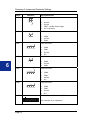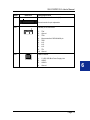
1
SK-S12XDP512-A
(Freescale Code EVB9S12XDP512)
Starter Kit for
Freescale MC9S12XDP512
User’s Manual
Revision 1.0
Copyright © 2005 SofTec Microsystems®
DC00854
We want your feedback!
SofTec Microsystems is always on the look-out for new ways to improve its
Products and Services. For this reason feedback, comments, suggestions or
criticisms, however small, are always welcome.
SofTec Microsystems
E-mail (general information): [email protected]
E-mail (marketing department): [email protected]
E-mail (technical support): [email protected]
Web: http://www.softecmicro.com
Important
SofTec Microsystems reserves the right to make improvements to the SK-S12XDP512-A Starter Kit, its documentation and
software routines, without notice. Information in this manual is intended to be accurate and reliable. However, SofTec
Microsystems assumes no responsibility for its use; nor for any infringements of rights of third parties which may result from its
use.
SOFTEC MICROSYSTEMS WILL NOT BE LIABLE FOR DAMAGES RESULTING FROM LOSS OF DATA, PROFITS, USE OF
PRODUCTS, OR INCIDENTAL OR CONSEQUENTIAL DAMAGES, EVEN IF ADVISED OF THE POSSIBILITY THEREOF.
Trademarks
Freescale™ and the Freescale logo are trademarks of Freescale Semiconductor, Inc.
Metrowerks and CodeWarrior are trademarks or registered trademarks of Metrowerks Corp.
Microsoft and Windows are trademarks or registered trademarks of Microsoft Corporation.
PC is a registered trademark of International Business Machines Corporation.
Other products and company names listed are trademarks or trade names of their respective companies.
Written by Loris Pacquola and Pietro Poletto. Graphics by Luisa Polesel. Edited by Paolo Xausa.
SK-S12XDP512-A User's Manual
Contents
0
Before Starting 9
0.1 Important Notice to Users 9
0.2 Required Skills 9
1
Overview 11
1.1 What is the SK-S12XDP512-A Starter Kit? 11
1.2 HCS12X Family Overview 12
1.3 MC9S12XDP512 Overview 12
1.3.1 XGATE Module Overview 13
1.3.2 Controller Area Network (CAN) Overview 13
1.3.3 Local Interconnect Network (LIN) Overview 14
1.3.4 FlexRay Overview 15
1.3.5 Background Debug Module (BDM) 16
1.4 CodeWarrior Development Studio Special Edition 17
1.5 Recommended Reading 17
1.6 Software Upgrades 18
1.7 Getting Technical Support 18
2
Hardware Features 19
2.1 The Evaluation Board 19
2.1.1 MCU Section 21
2.1.2 Reset Section 22
2.1.3 Inputs Section 23
2.1.4 MCU Settings Jumpers 24
2.1.5 ATD Reference Section 26
2.1.6 BDM Connector 27
2.1.7 USB to BDM Section 27
2.1.8 Power Supply Section 28
2.1.9 Outputs Section 29
2.1.10 CAN Section 31
Contents
2.1.11
2.1.12
2.1.13
2.1.14
2.1.15
3
LIN Section 32
RS-232 Section 33
Serial Settings Section 34
FlexRay Section 35
Prototype Area 35
Getting Started 37
3.1
3.2
3.3
3.4
Starter Kit Components 37
Standalone Example 37
Host System Requirements 38
Installing the Software 38
3.4.1 Installing CodeWarrior Development Studio 39
3.4.2 Installing SofTec Microsystems Additional Components 39
3.5 Installing the Hardware 40
3.6 Application Tutorial 43
3.7 Additional Examples 47
4
Debugging Features 49
4.1 Creating Your Own Application 49
4.1.1 Using the Project Wizard to Create Your Application
Skeleton 49
4.1.2 Starting your First Debugging Session 49
4.2 Using Existing Projects with SK-S12XDP512-A 50
4.3 Breakpoints and Trace 51
4.4 Notes and Tips 52
4.4.1 Reading Peripheral Status 52
4.4.2 Breakpoints and BGND Instruction 52
4.4.3 STOP Assembly Instruction 52
4.4.4 WAIT Assembly Instruction 52
4.4.5 Microcontroller Peripheral Running when Execution is
Stopped 53
4.4.6 Real-Time Memory Update 53
4.4.7 PLL Usage 53
4.4.8 Hardware Breakpoints and Software Breakpoints 53
4.4.9 Advanced Debugging Features 54
SK-S12XDP512-A User's Manual
4.5 DataBlaze Programming Utility 54
4.5.1 DataBlaze Notes 55
5
Troubleshooting 57
5.1 Common Problems and Solutions 57
5.1.1 USB Driver Problems 57
5.1.2 Communication Errors when Using a BDM Tool 58
5.1.3 The POWER LED Doesn’t Turn On 58
5.1.4 Communication Can’t Be Established with the Board 58
5.2 Getting Technical Support 59
6
Summary of Jumper and Connector Settings 61
6.1 Jumpers Summary 61
6.2 Connectors Summary/Pinout 70
7
Electrical Specifications 75
7.1 Absolute Maximum Ratings 75
7.2 Recommended Operating Conditions 75
SK-S12XDP512-A User's Manual
Index of Figures
Figure 2.1: The SK-S12XDP512-A Evaluation Board 19
Figure 2.2: Block Diagram of SK-S12XDP512-A 21
Figure 2.3: Block Diagram of the Reset Section 23
Figure 2.4: Block Diagram of the Inputs Section 24
Figure 2.5: Block Diagram of the MCU Settings Section 25
Figure 2.6: Block Diagram of the ATD Reference Section 26
Figure 2.7: Block Diagram of the BDM Section 27
Figure 2.8: Block Diagram of the USB to BDM Section 28
Figure 2.9: Block Diagram of the Power Supply Section 29
Figure 2.10: Block Diagram of the Outputs Section 30
Figure 2.11: Block Diagram of the CAN Section 32
Figure 2.12: Block Diagram of the LIN Section 33
Figure 2.13: Block Diagram of the RS-232 Section 34
Figure 3.1: New Hardware Wizard, Step 1 41
Figure 3.2: New Hardware Wizard, Step 2 41
Figure 3.3: New Hardware Wizard, Step 3 42
Figure 3.4: New Hardware Wizard, Step 4 43
Figure 3.5: The Project Window 44
Figure 3.6: The Example’s Source Code 45
Figure 3.7: Debugging Session Started 46
Figure 4.1: The MCU Configuration Dialog Box 49
Figure 4.2: The Set Target Dialog Box 50
Figure 4.3: The GDI Setup Dialog Box 50
Figure 4.4: The MCU Configuration Dialog Box 51
Figure 4.5: The DataBlaze User Interface 55
SK-S12XDP512-A User's Manual
0
0 Before Starting
0.1 Important Notice to Users
While every effort has been made to ensure the accuracy of all information in
this document, SofTec Microsystems assumes no liability to any party for
any loss or damage caused by errors or omissions or by statements of any
kind in this document, its updates, supplements, or special editions, whether
such errors are omissions or statements resulting from negligence,
accidents, or any other cause.
0.2 Required Skills
In order to beneficially use the SK-S12XDP512-A Starter Kit, you should be
acquainted with certain skills, ranging from hardware design to software
design. In particular, you should possess knowledge of the following:
Microcontroller systems;
HCS12X architecture knowledge;
Programming knowledge (Assembly and C);
CAN/LIN knowledge.
Page 9
SK-S12XDP512-A User's Manual
1 Overview
1.1 What is the SK-S12XDP512-A Starter Kit?
The SK-S12XDP512-A Starter Kit is a full-featured, ready-to-use evaluation
board for the MC9S12XDP512 microcontroller. The MC9S12XDP512 is a
member of the new Freescale HCS12X MCU family.
The SK-S12XDP512-A Starter Kit has been designed for the evaluation of
the MC9S12XDP512 microcontroller and the debugging of user applications.
The Starter Kit takes advantage of the CodeWarrior Development Studio
Special Edition (which groups an Editor, Assembler, C Compiler and
Debugger) and the Freescale BDM interface, which allows the download and
debug of the user application into the microcontroller’s FLASH memory.
Together with CodeWarrior, the Starter Kit provides you with everything you
need to write, compile, download, in-circuit emulate and debug user code.
Full-speed program execution allows you to perform hardware and software
testing in real time. The Starter Kit is connected to the host PC through a
USB port. A prototyping area allows you to wire your own small application.
The SK-S12XDP512-A Starter Kit offers you the following benefits:
Real-time code execution;
In-circuit debugging;
In-system programming and debugging through a BDM-compatible
interface;
Demo area with four push-buttons, a potentiometer, a photo sensor,
four user LEDs, two RS-232 ports and two dot matrix displays.
CAN area with five CAN connectors and five CAN transceivers;
LIN area with six LIN connectors and six LIN transceivers;
Two connectors for FlexRay expansion;
Prototyping area;
CodeWarrior Development Studio Special Edition (the same user
interface of all Freescale tools), with editor, assembler, C compiler and
debugger.
Page 11
1
Overview
1.2 HCS12X Family Overview
1
Targeted at automotive multiplexing applications, the HCS12X MCU family
delivers 32-bit performance with all the advantages and efficiencies of a 16bit MCU. Based around an enhanced HCS12 core, the HCS12X family
delivers 2 to 5 times the performance of a 25 MHz HCS12 while retaining a
high degree of pin and code compatibility with the HCS12.
The HCS12X family introduces the performance boosting XGATE module.
Using enhanced DMA functionality, this parallel processing module offloads
the CPU by providing high speed data processing and transfer between
peripheral modules, RAM and I/O ports. Providing up to 80 MIPS of
performance additional to the CPU, the XGATE can handle 64 channels and
is fully user programmable.
The HCS12XD family, in particular, features the enhanced MXCAN module
which, when used in conjunction with XGATE, delivers full CAN performance
with virtually unlimited number of mailboxes and retains backwards
compatibility with the MSCAN module featured on existing HCS12 products.
The inclusion of a PLL circuit allows power consumption and performance to
be adjusted to suit operational requirements. System power consumption is
further improved with the new “fast exit from STOP mode” feature and an
ultra low power wake-up timer.
1.3 MC9S12XDP512 Overview
The MC9S12XDP512 is composed of standard on-chip peripherals including
512 Kbytes of Flash, 32 Kbytes of RAM, 4 Kbytes of EEPROM, six
asynchronous serial communication interfaces (SCI), three serial peripheral
interfaces (SPI), an 8-channel IC/OC enhanced capture timer, an 8-channel,
10-bit analog-to-digital converter, a 16-channel, 10-bit analog-to-digital
converter, an 8-channel pulse-width modulator (PWM), five CAN 2.0A/B
software compatible modules (MSCAN12), two Inter-IC Bus blocks and a
Periodic Interrupt Timer. The MC9S12XDP512 has full 16-bit data paths
throughout. The non-multiplexed expanded bus interface available on the
144-pin versions allows an easy interface to external memories. The
MC9S12XDP512 is available in 144-pin LQFP with external bus interface
and in 112-pin LQFP or 80-pin QFP package without external bus interface.
Page 12
SK-S12XDP512-A User's Manual
1.3.1 XGATE Module Overview
The HCS12X microcontroller family offers many enhancements over the
HCS12 family; principal among these is the XGATE peripheral processor.
The XGATE module is a peripheral co-processor that allows autonomous
operation using on-chip RAM and peripherals, with zero load on the main
MCU’s core. The XGATE module is an event-driven RISC core machine. It
has its own instruction set and runs its own code. The code and data for the
XGATE module are stored in the on-chip RAM. Memory sharing is the main
method for exchanging data between different threads running on XGATE
and also between threads running on XGATE and the MCU’s core. From a
user’s perspective, the HCS12X family devices appear to be a multiprocessor environment and hardware semaphores are provided for
synchronization of tasks and resource management between threads
running on different cores. The XGATE executes its threads in response to
events. These events are issued by the interrupt module, based on its
configuration and signals from the on-chip peripherals and MCU core.
1.3.2 Controller Area Network (CAN) Overview
CAN (Controller Area Network) is a serial bus system, which was originally
developed for automotive applications in the early 1980’s. The CAN protocol
was internationally standardized in 1993 as ISO 11898-1 and comprises the
data link layer of the seven layer ISO/OSI reference model. CAN provides
two communication services: the sending of a message (data frame
transmission) and the requesting of a message (remote transmission
request, RTR). All other services such as error signaling, automatic retransmission of erroneous frames are user-transparent, which means the
CAN chip automatically performs these services.
The MC9S12XDP512 features five MSCAN (Motorola Scalable Controller
Area Network) modules. The basic features of the MSCAN modules are as
follows:
Implementation of the CAN protocol - Version 2.0A/B
•
Standard and extended data frames
•
0 - 8 bytes data length
•
Programmable bit rate up to 1 Mbps
•
Support for remote frames
Page 13
1
Overview
5 receive buffers with FIFO storage scheme
3 transmit buffers with internal prioritization using a “local priority”
concept
Flexible maskable identifier filter supports two full size extended
identifier filters (two 32-bit) or four 16-bit filters or eight 8-bit filters
Programmable wake-up functionality with integrated low-pass filter
Programmable loop back mode supports self-test operation
Programmable listen-only mode for monitoring of CAN bus
Programmable Bus-Off recovery functionality
Separate signalling and interrupt capabilities for all CAN receiver and
transmitter error states (Warning, Error Passive, Bus-Off)
Programmable MSCAN clock source either Bus Clock or Oscillator
Clock
Internal timer for time-stamping of received and transmitted messages
Three low power modes: Sleep, Power Down and MSCAN Enable
Global initialization of configuration registers
1
i
Note: the Starter Kit features five CAN transceivers (two
MC33388, two PCA82C250 and one MC33989) plus a provision
for two additional PCA82C250 transceivers.
Detailed information about the CAN bus and related protocols is beyond the
scope of this user manual. Full information is easily available from other
sources. We suggest visiting the http://www.can-cia.org and
http://www.can.bosch.com sites. On our CD you’ll find the CAN Bosch
specification.
1.3.3 Local Interconnect Network (LIN) Overview
LIN (Local Interconnect Network) is used as an in-vehicle (Automotive)
communication and networking serial bus between intelligent sensors and
actuators operating at 12 volts. Other auto body electronics include air
conditioning systems, doors, seats, column, climate control, switch panel,
intelligent wipers, and sunroof actuators. The LIN specification covers the
Page 14
SK-S12XDP512-A User's Manual
transmission protocol (Physical Layer and the Data Link Layer of LIN), and
the transmission medium. The maximum communication speed on a LIN bus
is 19200 baud (a 1 KOhm termination pull-up resistor is required). The LIN
Bus is a class A protocol operating at a maximum bus speed of 19200 baud
over a maximum cable length of 40 meters. LIN nodes can send/receive a
full 8 byte command every 10 ms (or shorter commands every 5 ms). The
LIN specification will also handle 2400, and 9600 baud rates, and may be
used as a sub-bus (sub-network) for a CAN bus interface. The LIN bus uses
a Master/Slave approach, having one Master and one or more Slaves. The
LIN bus does not need to resolve bus collisions because only one message
is allowed on the bus at a time.
i
Note: the MC9S12XDP512 microcontroller features six
asynchronous Serial Communication Interfaces (SCI) with
additional LIN support. The Starter Kit features six LIN transceivers
(MC33661).
Detailed information about the LIN bus and related protocols is beyond the
scope of this user manual. Full information is easily available from other
sources. We suggest visiting the http://www.lin-subbus.org and
http://www.can.bosch.com/LIN/LIN.html sites.
1.3.4 FlexRay Overview
FlexRay is a communication system that will support the needs of future incar control applications. At the core of the FlexRay system is the FlexRay
communications protocol. The protocol provides flexibility and determinism
by combining a scalable static and dynamic message transmission,
incorporating the advantages of familiar synchronous and asynchronous
protocols. The protocol also supports:
Fault-tolerant clock synchronization via a global time base;
Collision-free bus access;
Guaranteed message latency;
Message oriented addressing via identifiers;
Page 15
1
Overview
Scalable system fault-tolerance via the support of either single or dual
channels.
1
A physical layer incorporating an independent Bus Guardian provides further
support for error containment. The FlexRay system is targeted to support
data rates of up to 10 Mbit/sec with increased flexibility for easy system
extension and the dynamic use of bandwidth. The 10 Mbit/sec data rate is
available on two channels, giving a gross data rate of up to 20 Mbit/sec.
Detailed information about the FlexRay protocol is beyond the scope of this
user manual. Full information is easily available from other sources. We
suggest visiting the http://www.flexray.com site.
1.3.5 Background Debug Module (BDM)
All MCUs in the HCS12X family contain a single-wire background debug
interface which supports in-circuit programming of on-chip non-volatile
memory and sophisticated non-intrusive debug capabilities. This system
does not interfere with normal application resources. It does not use any
user memory or locations in the memory map and does not share any onchip peripherals. The background debug module (BDM) uses a single-wire
communication interface to allow non-intrusive access to target system
memory and registers.
The Starter Kit features a USB-to-BDM circuitry which allows the host PC to
communicate with the microcontroller through a standard USB cable.
Contrariwise to traditional in-circuit emulation (where the target application is
executed and emulated inside the emulator), the Starter Kit uses the very
same target microcontroller to carry on in-circuit execution. This means that
all microcontroller’s peripherals (timers, A/D converters, I/O pins, etc.) are
not reconstructed or simulated by an external device, but are the very same
target microcontroller’s peripherals. Moreover, the Starter Kit debugging
approach ensures that the target microcontroller’s electrical characteristics
(pull-ups, low-voltage operations, I/O thresholds, etc.) are 100% guaranteed.
Page 16
SK-S12XDP512-A User's Manual
1.4 CodeWarrior Development Studio Special
Edition
The SK-S12XDP512-A Starter Kit comes with CodeWarrior Development
Studio Special Edition for Freescale HC9S12X/XGATE Microcontrollers.
CodeWarrior Development Studio for HC9S12X/XGATE is a powerful and
easy-to-use tool suite designed to increase your software development
productivity. Its Integrated Development Environment (IDE) provides
unrivaled features such as Processor Expert application design tool, full chip
simulation, Data Visualization and project manager with templates to help
you concentrate on the added value of your application.
The comprehensive, highly visual CodeWarrior Development Studio for
Freescale HC9S12X/XGATE Microcontrollers enables you to build and
deploy HC9S12X/XGATE systems quickly and easily. This tool suite
provides the capabilities required by every engineer in the development
cycle, from board bring-up to firmware development to final application
development.
Without a license key, the product will run in a 1 KB code-size limited
demonstration mode.
To break the 1 KB limit, you have two options:
1.
2.
Contact Metrowerks to request an unlimited period, free license key to
increase the code size limit to 32 KB;
Contact Metrowerks to request a 30-day limited, free license key to run
the compiler without limitations.
This documentation covers the basic setup and operation of CodeWarrior
Development Studio, but does not cover all of its functions. For further
information, please refer to the CodeWarrior on-line help and on-line
documentation provided.
1.5 Recommended Reading
This documentation describes how to use the SK-S12XDP512-A Starter Kit
and how to set up basic debugging sessions with CodeWarrior. Additional
information can be found in the following documents:
Page 17
1
Overview
MC9S12XDP512 Datasheets;
MC9S12XDP512 Application Note;
SK-S12XDP512-A Schematic.
1
All of the above documents (and many more) are available in the SKS12XDP512-A “System Software” CD-ROM.
i
Note: the SofTec Microsystems “System Software” CD-ROM also
contains the datasheets of every component used in the Starter
Kit.
1.6 Software Upgrades
The latest version of the SK-S12XDP512-A system software is always
available free of charge from our website: http://www.softecmicro.com.
When installing the SK-S12XDP512-A system software you have the option
to electronically register the product. If you register the product, you will be
automatically notified by e-mail every time a new version of the SKS12XDP512-A system software is available.
1.7 Getting Technical Support
Technical assistance is provided to all customers. For technical assistance,
documentation and information about products and services, please refer to
your local SofTec Microsystems partner.
SofTec Microsystems offers its customers a technical support service at
[email protected]. Before getting in contact with us, we advise you
to check that you are working with the latest version of the SK-S12XDP512A system software (upgrades are available free of charge at
http://www.softecmicro.com).
Page 18
SK-S12XDP512-A User's Manual
2 Hardware Features
2.1 The Evaluation Board
The following figure illustrates the main functions of the evaluation board.
10
11
9
6
8
12
7
13
1
5
4
14
3
15
2
Figure 2.1: The SK-S12XDP512-A Evaluation Board
Page 19
2
Hardware Features
2
1.
2.
3.
4.
5.
6.
7.
8.
9.
10.
11.
12.
13.
14.
15.
MCU, oscillator, and signal pins section.
Reset section.
Inputs section.
MCU settings jumpers.
ATD reference section.
BDM connector.
USB to BDM interface.
Power supply section.
Outputs section.
CAN section.
LIN section.
RS-232 section.
Serial settings.
FlexRay connectors.
Prototype area.
The following figure shows the SK-S12XDP512-A board block diagram.
Page 20
SK-S12XDP512-A User's Manual
2
Figure 2.2: Block Diagram of SK-S12XDP512-A
2.1.1 MCU Section
An MC9S12XDP512 microcontroller (in LQFP144 package) is soldered in
this area. The microcontroller is surrounded by a network of filter capacitors.
A jumper (“XFC SEL”) allows enabling either the built-in RC loop filter
(needed for the microcontroller’s internal PLL) or a user-made RC loop filter.
All of the microcontroller’s signals are available at the four header
connectors which surround the microcontroller. However, some lines are not
Page 21
Hardware Features
2
taken directly from the microcontroller. For example, the EXTAL and XTAL
lines are not present in the header connectors because, if they were, the
clock signal would have been degraded by the lengthy PCB track. Other
signals, such as XFC, VRL and VRH, are not directly tied to the header
connectors but pass through the jumpers instead.
Two clock sources are available: a socketed oscillator module and a 4 MHz
crystal, selectable via the “OSC SEL” jumper.
The oscillator module output is filtered by a RC network, which adapts the
oscillator’s output voltage range (0 to 5 V) to the maximum voltage range
accepted by the microcontroller’s EXTAL pin (0 to 2.5 V).
The crystal and the module oscillator can be configured (via the
“XCLKS#=0” and the “OSC SEL” jumpers) to generate various clock types,
as summarized in the table below.
“XCLKS#=0”
Jumper
“OSC SEL”
Jumper
Oscillator Source Selected
Inserted
CLOCK
Clock Module (16 MHz Installed)
Inserted
CRYSTAL
4 MHz Crystal (Full Swing Pierce Oscillator)
Not inserted
CRYSTAL
4 MHz Crystal (Loop Controlled Pierce
oscillator)
Not inserted
CLOCK
Illegal
2.1.2 Reset Section
This section groups a reset push-button and a reset supervisor circuitry. The
reset supervisor circuitry generates a suitable reset signal (for the
MC9S12XDP512 microcontroller and for the peripheral connected to it)
every time the Starter Kit is powered on and after a low-voltage detect event.
The reset supervisor circuitry (enabled by default) can be disabled by
removing the “LVD ENA” jumper.
Page 22
SK-S12XDP512-A User's Manual
2
Figure 2.3: Block Diagram of the Reset Section
2.1.3 Inputs Section
This area contains various input controls: a potentiometer, a light sensor
(photoresistor) and four push-buttons.
The potentiometer (connected to the MC9S12XDP512’s PAD10 pin through
a jumper) provides an output voltage in the range between 0 V and VDD.
A photoresistor (pulled to VDD) is connected to the MC9S12XDP512’s
PAD11 pin through a jumper.
Four push-buttons are connected to the microcontroller’s PB7, PB6, PB5
and PB4 lines, respectively, through a 470 Ohm serial resistor.
The 470 Ohm serial resistor prevents accidental short circuits in the case
that the microcontroller port is configured as a push-pull output, a logic “1” is
written to the port, and the push-button is pressed.
i
Note: to read the status of the push-buttons, the respective
microcontroller port’s internal pull-ups must be enabled.
Page 23
Hardware Features
2
Figure 2.4: Block Diagram of the Inputs Section
2.1.4 MCU Settings Jumpers
This area contains four jumpers to set the internal voltage regulator and the
operating mode of the microcontroller.
The VREGEN jumper selects whether the on-chip voltage regulator is
enabled or disabled.
i
Note: if the internal voltage regulator is disabled, VDD1, VDD2 and
VDDPLL must be supplied externally.
The operating mode out of reset is determined by the states of the MODC,
MODB, and MODA pins (see table below).
Page 24
SK-S12XDP512-A User's Manual
“MODC”
Jumper
“MODB=1”
Jumper
“MODA=1”
Jumper
Microcontroller Mode Operations
“0” Position
Not inserted
Not inserted
Special Single Chip Mode
“0” Position
Inserted
Inserted
Emulation Expanded Mode
“0” Position
Inserted
Not inserted
Special Test Mode
“0” Position
Not inserted
Inserted
Emulation Single Chip Mode
“1” Position
Not inserted
Not inserted
Normal Single Chip Mode (default)
“1” Position
Not inserted
Inserted
Normal Expanded Mode
“1” Position
Inserted
Not inserted
Reserved
“1” Position
Inserted
Inserted
Reserved
When debugging the microcontroller using an in-circuit debugger (via the
BDM connector) or using the built-in USB connector, it is recommended to
remove the “MODA=1” and “MODB=1” jumpers. Additionally, the “MODC”
jumper must select the “1” position (the in-circuit debugger will automatically
pull the line to 0 when entering the Special Single Chip Mode).
i
Note: the states of the MODC, MODB and MODA pins are latched
into these bits on the rising edge of RESET.
Figure 2.5: Block Diagram of the MCU Settings Section
Page 25
2
Hardware Features
2.1.5 ATD Reference Section
2
This area contains two jumpers which allow you to define the high (VRH)
and low (VRL) voltage reference for the MCU’s internal A/D converter.
It is possible to set VRH to an internal reference voltage (obtained from the
board’s VDD voltage and filtered by an LC network) or to an external
reference defined by the user.
Similarly, it is possible to set VRL to an internal reference voltage (the
board’s ground) or to an external reference defined by the user.
i
Note: when the “VRH SEL” or “VRL SEL” jumpers are set to
“USER”, the VRH and VRL voltages must comply with the data
reported in the table below.
Reference Signal
Min
Max
VRL
VSSA = GND
VDDA / 2
VRH
VDDA / 2
VDDA
Differential Reference Voltage
VRH-VRL
4.5 V
5.5 V
Figure 2.6: Block Diagram of the ATD Reference Section
Page 26
SK-S12XDP512-A User's Manual
2.1.6 BDM Connector
Even though the Starter Kit features a built-in USB to BDM interface, a
separate BDM connector is present which allows an external in-circuit
debugger to be used.
i
Note: to bypass the built-in USB to BDM interface when using an
external in-circuit debugger, please remove the “RESET ENA”
and “BKGD ENA” jumpers in the “USB TO BDM” section.
Figure 2.7: Block Diagram of the BDM Section
2.1.7 USB to BDM Section
The Starter Kit features a built-in USB to BDM interface, that is, a circuitry
that electrically and logically translates BDM-like commands sent by the host
PC through the USB cable to the BDM interface of the MC9S12XDP512
microcontroller.
The USB to BDM interface is based on a Freescale MC9S12UF32
microcontroller, which features an on-board, USB 2.0 peripheral.
Page 27
2
Hardware Features
i
Note: to bypass the built-in USB to BDM interface when using an
external in-circuit debugger (via the BDM connector), please
remove the “RESET ENA” and “BKGD ENA” jumpers.
2
Figure 2.8: Block Diagram of the USB to BDM Section
2.1.8 Power Supply Section
The Power Supply section takes a 12 V DC voltage (used for the LIN and
CAN transceivers) and, thanks to the built-in switching power supply,
provides a regulated, 5 V DC voltage for the rest of the board (VDD), with a
maximum current of 0.7 A.
A 0.75 A auto-restore fuse protects the board from accidental short circuits.
The built-in switching power supply circuitry can be disabled by removing the
“VDD ENA” jumper; this allows you to provide your own voltage for the VDD
line. When doing this, make sure that the provided voltage doesn’t exceed
Page 28
SK-S12XDP512-A User's Manual
5.5 V DC, otherwise the microcontroller and other parts of the board may be
damaged.
A dedicated, 5 V linear regulator provides the required voltage to the “USB
TO BDM” section.
An EMI filter improves the system tolerance to electric noise on the power
supply line.
2
Figure 2.9: Block Diagram of the Power Supply Section
2.1.9 Outputs Section
This area contains four high-efficiency (low-current) LEDs and two 7x5 dotmatrix displays.
The LEDs are connected to the microcontroller’s PB[3..0] port, with four
jumpers to connect/disconnect each of the four LEDs to/from their respective
Port PB pins.
The two dot-matrix displays are driven by the microcontroller’s PA[6..0] ports
(common rows), PC[4..0] ports (columns for the first display) and PD[4..0]
ports (columns for the second display). Each dot in the dot-matrix displays is
actually a LED.
In order to decrease the number of lines needed to drive the two dot-matrix
displays, a multiplexing technique has been used.
Page 29
Hardware Features
2
At the beginning, only the first “column” of LEDs in the first display is
enabled, using the microcontroller’s PC0 line, while each “row” of LEDs is
set to the desired value, using the microcontroller’s PA[6..0] lines. Then, the
column is disabled and the next column (PC1 line) is enabled, and the
microcontroller’s PA[6..0] lines are set appropriately, and so on, until the last
column of the first display (PC4) is updated.
The same goes for the second display (this time using the microcontroller’s
PD[4..0] line to enable the columns).
Each column of LEDs is therefore turned on only for a limited amount of
time, while the other columns are off. By refreshing the columns with a
sufficiently high rate, the human eye perceives the whole display turned on.
Figure 2.10: Block Diagram of the Outputs Section
Page 30
SK-S12XDP512-A User's Manual
2.1.10 CAN Section
Two fault-tolerant (up to 125 Kbaud) CAN transceivers and three high-speed
(up to 1 Mbaud) CAN transceivers are at the heart of the Starter Kit, for a
total of five CAN nodes.
Two additional high-speed transceivers (PCA82C250) can be soldered on
the PCB.
The following table lists each CAN node together with its associated
transceiver and connector.
CAN Node
Number
CAN Node Type
Transceiver Used
Connector Type
CAN0
Fault Tolerant
(High speed with the
optional PCA82C250
transceiver)
MC33388
(An optional
PCA82C250 can be
soldered )
3x1 Male Header
CAN1
Fault Tolerant
(High speed with the
optional PCA82C250
transceiver)
MC33388
(An optional
PCA82C250 can be
soldered )
4-Way Box
CAN2
High Speed
PCA82C250
3x1 Male Header
CAN3
High Speed
MC33989
4-Way Box
CAN4
High Speed
PCA82C250
4-Way Box
The TX and RX signals of CAN nodes CAN0, CAN1, CAN2 and CAN4 can
be disconnected (by removing the respective “CANx TX ENA” and “CANx
RX ENA” jumpers) from the MC9S12XDP512’s respective pins.
Please note that the MC9S12XDP512’s RX and TX lines used by the CAN3
node are shared with LIN3’s RX and TX lines. Use the “CAN3/LIN3 SEL”
jumper in the “SERIAL SETTINGS” section of the board to select whether to
use the CAN3 node, the LIN3 node, or to free the MC9S12XDP512’s RX
and TX lines associated with these nodes.
Additionally, CAN nodes CAN0 e CAN1 have additional jumpers to select
whether to use the on-board MC33388 fault-tolerant transceivers (default) or
the optional PCA82C250 high-speed transceivers (optional, to be soldered).
Page 31
2
Hardware Features
2
Figure 2.11: Block Diagram of the CAN Section
2.1.11 LIN Section
Six LIN transceivers are used to handle six LIN nodes, each capable of a
speed of up to 100 Kbps in fast mode. Three LIN nodes use a 3x1 header
connector, while the other three nodes use a 4-way box connector.
Every LIN node can be configured as a master node via its respective
“MASTER NODEx ENA” jumper, which inserts a 900 Ohm resistor between
the LIN bus line and the LIN bus power supply line.
The LIN transceivers can be powered either by the Starter Kit’s internal 12 V
DC reference, or by the LIN network itself, via the “LIN TRANSCEIVER
SUPPLY SEL” jumper.
Analogously, the LIN network can be supplied by the Starter Kit’s internal 12
V DC reference via the “LIN SUPPLY ENA” jumper.
The TX and RX signals of LIN nodes LIN2, LIN4 and LIN5 can be
disconnected (by removing the respective “LINx TX ENA” and “LINx RX
ENA” jumpers) from the MC9S12XDP512’s respective SCI pins.
Page 32
SK-S12XDP512-A User's Manual
Please note that the MC9S12XDP512’s RX and TX lines used by the LIN0
and LIN1 nodes are shared with RS-232 0 and RS-232 1’s RX and TX lines,
respectively. Use the “RS-232_x/LINx SEL” jumpers in the “SERIAL
SETTINGS” section of the board to select whether to use the RS-232 node,
LIN node, or to free the MC9S12XDP512’s RX and TX lines associated with
these nodes.
Additionally, please note that the MC9S12XDP512’s RX and TX lines used
by the LIN3 node are shared with CAN3’s RX and TX lines. Use the
“CAN3/LIN3 SEL” jumper in the “SERIAL SETTINGS” section of the board
to select whether to use the CAN3 node, the LIN3 node, or to free the
MC9S12XDP512’s RX and TX lines associated with these nodes.
Figure 2.12: Block Diagram of the LIN Section
2.1.12 RS-232 Section
Two RS-232 channels are available, thanks to an RS-232 transceiver
(MAX3232) that is connected to the microcontroller’s SCI0 and SCI1 serial
communication interfaces. The two RS-232 channels are EIA/TIA-232-F
compliant (up to 250 Kbit/s).
Page 33
2
Hardware Features
Each RS-232 channel can be configured as DTE (Data Transmission
Equipment) or DCE (Data Communication Equipment) via the relative
jumper.
2
Figure 2.13: Block Diagram of the RS-232 Section
Please note that the SCI0 and SCI1 microcontroller peripherals are shared
with the LIN section of the Starter Kit.
2.1.13 Serial Settings Section
This section of the Starter Kit has three jumpers that allow the selection of
how to use the SCI0, SCI1 and SCI3 peripherals of the MC9S12XDP512.
The SCI0 peripheral can be connected to the LIN0 node or to the RS-232
channel 0, or can be freed by removing all jumpers.
The SCI1 peripheral can be connected to the LIN1 node or to the RS-232
channel 1, or can be freed by removing all jumpers.
The SCI3 peripheral can be connected to the LIN3 node or to the CAN3
node, or can be freed by removing all jumpers.
Page 34
SK-S12XDP512-A User's Manual
2.1.14 FlexRay Section
This area contains two 50-way connectors that can be used for FlexRay
expansion.
The layout of these two connectors is compliant with the IP Modules
ANSI/VITA 4-1995 standard.
A JTAG connector allows the interfacing of optional JTAG peripherals
mounted on the FlexRay expansion board.
2.1.15 Prototype Area
The prototype section features both a standard, thru-hole area (for mounting
traditional components) and a SMD area (for soldering SMD components in
SOIC, SSOP/TSSOP package).
Page 35
2
SK-S12XDP512-A User's Manual
3 Getting Started
3.1 Starter Kit Components
The SK-S12XDP512-A package includes the following items:
A full-featured evaluation board;
An AC adapter;
A USB cable;
The SofTec Microsystems SK-S12XDP512-A “System Software” CDROM;
The CodeWarrior Development Studio Special Edition CD-ROM;
A QuickStart Tutorial poster;
A registration card;
This user’s manual.
3.2 Standalone Example
The Starter Kit comes pre-programmed with a sample application that can
be executed without being connected to the PC. To run the built-in example:
1.
2.
3.
Verify that all jumpers are in their default position. See the “Summary of
Jumper and Connector Settings” chapter.
Power the demo board. The power connector accepts 12 V DC wall
plug-in power supply with a 2.1 mm pin and sleeve plug with positive in
the center and sleeve as ground. Make sure the “VDD ENA” jumper is
inserted. The voltage is internally regulated to 5.0 V DC. The green
“POWER” LED on the board should turn on.
Press the “PB4” push-button. The output of the light sensor will be
displayed on the two dot-matrix displays, in a graphic way. The light
sensor is placed on the right of the “PB4” push-button. Cover the
sensor with a finger and see the effect on the displays.
Page 37
3
Getting Started
4.
Press the “PB5” push-button. The output of the light sensor will be
displayed on the two dot-matrix displays, in a numeric (hexadecimal)
way.
Press the “PB6” push-button. The value of the PAD10 potentiometer
will be displayed on the two dot-matrix displays, in a graphic way.
Press the “PB7” push-button. The value of the PAD10 potentiometer
will be displayed on the two dot-matrix displays, in a numeric
(hexadecimal) way.
5.
6.
3
3.3 Host System Requirements
The SK-S12XDP512-A Starter Kit is controlled by an Integrated
Development Environment running under Windows (CodeWarrior for
HC9S12X/XGATE). The following hardware and software are required to run
the CodeWarrior for HC9S12X/XGATE user interface together with SKS12XDP512-A:
1.
A 200-MHz (or higher) PC compatible system running Windows 98,
Windows 2000 or Windows XP;
128 MB of available system RAM plus 500 MB of available hard disk
space;
A USB port;
CD-ROM drive for installation.
2.
3.
4.
3.4 Installing the Software
i
Page 38
Note: before connecting the SK-S12XDP512-A board to the PC, it
is recommended that you install all of the required software first
(see below), so that the SK-S12XDP512-A USB driver will be
automatically found by Windows when you connect the board.
SK-S12XDP512-A User's Manual
The Starter Kit requires that both CodeWarrior Development Studio Special
Edition and SofTec Microsystems Additional Components be installed in the
host PC.
i
Note: CodeWarrior Development Studio for HC9S12X/XGATE
must be installed first. Please note that the Starter Kit only works
with CodeWarrior for HC9S12X/XGATE version 4.1 or above.
3
3.4.1 Installing CodeWarrior Development Studio
To install the CodeWarrior Development Studio Special Edition, insert the
CodeWarrior CD-ROM into your computer’s CD-ROM drive. A startup
window will automatically appear. Follow the on-screen instructions.
3.4.2 Installing SofTec Microsystems Additional Components
The SofTec Microsystems Additional Components install all of the other
required components to your hard drive. These components include:
The SK-S12XDP512-A USB driver;
The SK-S12XDP512-A software plug-in for CodeWarrior for
HC9S12X/XGATE;
DataBlaze programming utility;
Examples;
Documentation in PDF format.
To install the SofTec Microsystems Additional Components, insert the
SofTec Microsystems “System Software” CD-ROM into your computer’s
CD-ROM drive. A startup window will automatically appear. Choose “Install
Instrument Software” from the main menu. A list of available software will
appear. Click on the “SK-S12XDP512-A Additional Components” option.
Follow the on-screen instructions.
Page 39
Getting Started
i
Note: to install the SK-S12XDP512-A Additional Components on
Windows 2000 or Windows XP, you must log in as Administrator.
3.5 Installing the Hardware
3
The SK-S12XDP512-A board is connected through a USB port to a host PC.
Connection steps are listed below in the recommended flow order:
1.
2.
3.
4.
5.
Install all the required system software as described in the previous
section.
Power up the demo board. The power connector accepts 12 V DC, wall
plug-in power supply with a 2.1 mm pin and sleeve plug with positive in
the center and sleeve as ground. Make sure the “VDD ENA” jumper is
inserted. The voltage is internally regulated to 5.0 V DC. The green
“POWER” LED on the board should turn on.
Insert one end of the USB cable into a free USB port.
Insert the other end of the USB cable into the USB connector on the
SK-S12XDP512-A board.
The first time the Starter Kit is connected to the PC, Windows
recognizes the instrument and starts the “Found New Hardware
Wizard” procedure, asking you to specify the driver to use for the
instrument. On Windows XP (SP2) the following dialog box will appear,
asking you to search for a suitable driver on the web.
Page 40
SK-S12XDP512-A User's Manual
3
Figure 3.1: New Hardware Wizard, Step 1
6.
Select the “No, not this time” option and click the “Next >” button.
The following dialog box will appear.
Figure 3.2: New Hardware Wizard, Step 2
7.
Click the “Next >” button.
Depending on your Windows settings, the following warning may
appear.
Page 41
Getting Started
3
Figure 3.3: New Hardware Wizard, Step 3
i
8.
Note: this warning is related to the fact that the USB driver
used by SK-S12XDP512-A is not digitally signed by
Microsoft, and Windows considers it to be potentially
malfunctioning or dangerous for the system. However, you
can safely ignore the warning, since every kind of
compatibility/security test has been carried out by SofTec
Microsystems.
Click the “Continue Anyway” button.
Windows will install the driver files to your system. At the end of the
installation, the following dialog box will appear.
Page 42
SK-S12XDP512-A User's Manual
3
Figure 3.4: New Hardware Wizard, Step 4
9.
Click the “Finish” button to exit from the “Found New Hardware
Wizard” procedure.
The Starter Kit’s USB driver is now installed on your system.
3.6 Application Tutorial
This section will provide a step-by-step guide on how to launch your first SKS12XDP512-A project and get started with the CodeWarrior for
HC9S12X/XGATE user interface.
The sample application is the same as the one described in the “Standalone
Example” section.
1.
2.
3.
4.
Ensure that the SK-S12XDP512-A Starter Kit is connected to the PC
(via the USB cable) and that the board is powered.
Make sure that all of the Starter Kit’s jumpers are set to their factory
position (see the “Jumpers Summary” section on page 61)
Start CodeWarrior Development Studio by selecting Start > Programs
> Metrowerks CodeWarrior > CW for HCS12X > CodeWarrior IDE.
CodeWarrior Development Studio will open.
From the main menu, choose “File > Open”. Select the “Demo.mcp”
workspace file that is located under the “\Program
Page 43
Getting Started
Files\Metrowerks\CW for HCS12X\(CodeWarrior_Examples)
\HCS12X\SofTec Microsystems\SK-S12XDP512-A\Demo” directory.
Click “Open”. The following window will appear.
3
Figure 3.5: The Project Window
5.
The C code of this example is contained in the “main.c” file. Double
click on it to open it. The following window will appear.
Page 44
SK-S12XDP512-A User's Manual
3
Figure 3.6: The Example’s Source Code
6.
7.
From the main menu, choose “Project > Debug”. This will compile the
source code, generate an executable file and download it to the demo
board.
A new debugger environment will open.
Page 45
Getting Started
3
Figure 3.7: Debugging Session Started
8.
From the main menu, choose “Run > Start/Continue”. The program
will be executed in real-time.
9. From the main menu, choose “Run > Halt”. The program execution will
stop. The next instruction to be executed is highlighted in the Source
window.
10. From the main menu, choose “Run > Single Step”. The instruction
highlighted in the Source window will be executed, and the program
execution will be stopped immediately after.
11. From the main menu, choose “Run > Start/Continue”. The application
will restart from where it was previously stopped.
Congratulations! You have successfully completed this tutorial! You can
continue to experiment with the CodeWarrior user interface and discover by
yourself its potentialities. For an in-depth guide of all of the user interface
Page 46
SK-S12XDP512-A User's Manual
features, select Help > CodeWarrior Help from CodeWarrior Development
Studio’s main menu.
3.7 Additional Examples
Additional examples can be found under the “\Program
Files\Metrowerks\CW for
HCS12X\(CodeWarrior_Examples)\HCS12X\SofTec Microsystems\SKS12XDP512-A” directory.
3
Page 47
SK-S12XDP512-A User's Manual
4 Debugging Features
4.1 Creating Your Own Application
4.1.1 Using the Project Wizard to Create Your Application Skeleton
CodeWarrior for HC9S12X/XGATE helps you get started with your own
application by including a project wizard specific for HCS12-based SofTec
Microsystems boards. To create a new project:
1.
2.
3.
From the main menu, select File > New”.
A dialog box will appear. Select “HC(S)12 New Project Wizard”.
Follow the Project Wizard steps, making sure you select the correct
microcontroller derivative you are working with (MC9S12XDP512) and
that the “SofTec Microsystems” target connection is used.
4.1.2 Starting your First Debugging Session
The first time you enter a debugging session (by selecting “Project >
Debug” from the CodeWarrior’s main menu) the MCU Configuration dialog
box will open, asking you to select the debugging hardware connected to the
PC. Make sure that the hardware code is set to “SK-S12XDP512-A”.
Figure 4.1: The MCU Configuration Dialog Box
Page 49
4
Debugging Features
4.2 Using Existing Projects with SK-S12XDP512-A
If your project has been targeted to an emulator/simulator other than SKS12XDP512-A and you wish to use SK-S12XDP512-A as the debugger for
your project, please do the following:
1.
CodeWarrior is interfaced to the SK-S12XDP512-A engine through a
so-called “GDI interface”. From the CodeWarrior debugger interface,
select Component > Set Target and choose “HC12” as processor and
“GDI Target Interface” as target interface.
4
Figure 4.2: The Set Target Dialog Box
2.
A dialog box will appear asking you to locate the GDI DLL file needed to
interface with SK-S12XDP512-A. Select the SofTec_BDM12.dll file
located into the \Program Files\Metrowerks\ CW for HCS12X\prog\
directory.
Figure 4.3: The GDI Setup Dialog Box
Page 50
SK-S12XDP512-A User's Manual
3.
The MCU Configuration dialog box will appear allowing you to select the
SK-S12XDP512-A board as the hardware debugger.
Figure 4.4: The MCU Configuration Dialog Box
4.
On the CodeWarrior debugger interface a new menu (“inDARTHCS12”) will be created. From this menu, select “Load” and locate the
object file your project is based on.
i
Note: the SK-S12XDP512-A Starter Kit is based on the SofTec
Microsystems’ inDART debugging engine.
4.3 Breakpoints and Trace
CodeWarrior offers a variety of tools for analyzing the program flow:
breakpoints (both simple and complex), watchpoints and a trace buffer. All
these features are implemented by taking advantage of the target
microcontroller’s debug peripheral.
i
Note: when setting an instruction breakpoint on a RAM location, a
software breakpoint is set (the opcode present at that location is
automatically replaced by the BGND Assembly instruction).
Therefore, no hardware breakpoints are wasted.
Page 51
4
Debugging Features
i
Note: the Single Step command (in a C source code) and the Step
Over and Step Out commands (both in a C and Assembly source
code) use one hardware breakpoint.
4.4 Notes and Tips
4.4.1 Reading Peripheral Status
4
Care must be taken when reading some peripheral’s status/data registers,
since a reading operation may cause the clearing of flags. This may happen
when the Memory window or the Data window is open, since these windows
read microcontroller’s resources during refresh operations.
4.4.2 Breakpoints and BGND Instruction
The BGND Assembly instruction forces the target microcontroller to enter the
Active Background Debug mode, stopping program execution. CodeWarrior
recognizes this event as a breakpoint and updates the contents of registers,
memory, etc. Successive commands (Start/Continue, Single Step, etc.) will
continue the execution of the program from the next instruction.
4.4.3 STOP Assembly Instruction
The BDM peripheral doesn’t work in STOP mode. If, on the Condition Code
Register (CCR), the S bit is set, the STOP instruction will stop all the
microcontroller’s activities (and therefore the BDM peripheral). If, on the
other hand, the S bit is reset, the STOP instruction will be executed as two
NOP instructions.
4.4.4 WAIT Assembly Instruction
If the SYSWAI bit in the CLKSEL register has been set, the WAIT instruction
will cause a BDM communication loss. This is because the system clock is
suspended in WAIT mode, therefore stopping the BDM peripheral.
Page 52
SK-S12XDP512-A User's Manual
4.4.5 Microcontroller Peripheral Running when Execution is Stopped
When program execution is stopped, some peripherals will still run while
others will stop. Which ones stop and which ones don’t depend on the
particular peripheral architecture. For more information, please refer to the
microcontroller datasheets.
In particular, to cause the COP and RTI peripherals to stop when you stop
program execution, the RSBCK in the COPCTL register must have been
previously set.
4.4.6 Real-Time Memory Update
During program execution, it is possible to view/edit the contents of the
Memory window and Data window in real time (edit operations are only
available for RAM locations and peripheral registers). For example, it is
possible to set the periodical refresh of the Memory window contents by
choosing “Mode > Periodical” from the pop-up menu which appears by
right-clicking on the Memory window.
4.4.7 PLL Usage
The host PC communicates with the microcontroller through the “USB to
BDM INTERFACE” circuitry. The BDM communication speed depends on a
clock source, which in turn is selected by the CLKSW bit in the Status
register. If the CLKSW bit is set to 1, the BDM communication clock source
is the microcontroller’s bus frequency; if the CLKSW bit is set to 0, the BDM
communication clock source is a constant clock source (in the case of the
MC9S12XDP512, half the frequency of the external oscillator).
The CLKSW bit can be set (within a debugging session) via the
Communication Settings dialog box. To open the Communication Settings
dialog, choose “MCU Configuration” from the “inDART-HCS12” menu.
The MCU Configuration dialog box will appear. Press the “Communication
Settings” button.
4.4.8 Hardware Breakpoints and Software Breakpoints
A “hardware” breakpoint is set by taking advantage of the microcontroller’s
integrated debug peripheral. A hardware breakpoint doesn’t waste system
Page 53
4
Debugging Features
4
resources, you can set/remove them at any time (even during program
execution), but the number of available hardware breakpoints is limited.
A “software” breakpoint, on the other hand, does not take advantage of the
microcontroller’s integrated debug peripheral.
To set a software breakpoint, there are two possibilities: you can set a
software breakpoint in RAM or in FLASH. In both cases, an unlimited
number of software breakpoints can be set.
To set a software breakpoint in a RAM location, just insert a breakpoint to
that location: CodeWarrior will automatically replace the opcode present at
that location with the BGND Assembly instruction.
To set a software breakpoint in a FLASH location, you have to insert the
BGND Assembly instruction into your application’s source code, recompile
the code and restart a debug session. The program execution will stop as
soon as the BGND instruction is fetched.
4.4.9 Advanced Debugging Features
The MC9S12XDP512 microcontroller’s built-in DBG12 module allows you to
set “complex” hardware breakpoints and to take advantage of a trace buffer.
While in debug, under the “inDART-HCS12” menu you will find the “Trigger
Module Settings…” command, that opens a dedicated dialog box which
allows you to handle all of the parameters of the microcontroller’s debug
peripheral.
4.5 DataBlaze Programming Utility
A full-featured programming utility (DataBlaze) is also provided with the SKS12XDP512-A Starter Kit. To start the DataBlaze utility select Start >
Programs > SofTec Microsystems > SK-S12XDP512-A > DataBlaze
Programmer.
DataBlaze offers the following advanced features:
Code memory editing;
Blank check/erase/program/verify/read operations;
Project handling;
One-button, multiple-operations programming (“Auto” feature);
Page 54
SK-S12XDP512-A User's Manual
Serial numbering.
4
Figure 4.5: The DataBlaze User Interface
4.5.1 DataBlaze Notes
The “Mass Erase” operation always blanks the device (even if the
device is protected or secured) and “unsecures” the device (the FLASH
Options/Security Byte location is programmed with 0xFE).
The “Blank Check” operation doesn’t blank check the FLASH
Options/Security Byte location.
The “Program” operation automatically verifies the programmed data by
reading back the programmed data and checking it against the buffer
sent to the target device. The “Verify” operation is much more secure
(but slower), since it reads back the programmed data and checks it
against the data buffer present in the host PC.
In case of verifying error, please verify the value programmed to the
FLASH Options/Security Byte location. The bit 0 of this byte is always
Page 55
Debugging Features
programmed to 0, so any attempt to program it to 1 will cause a
verifying error.
In the “Auto” operation, a “Run” option is available which, if enabled,
resets the microcontroller and runs the user application at the end of
programming.
4
Page 56
SK-S12XDP512-A User's Manual
5 Troubleshooting
5.1 Common Problems and Solutions
This section reports some common problems that may arise during general
use.
5.1.1 USB Driver Problems
If you connected the SK-S12XDP512-A board to the PC before installing the
CodeWarrior user interface and the SofTec Microsystems Additional
Components, the SK-S12XDP512-A USB driver may not have been correctly
installed on your system. Unplugging and replugging the USB cable is of no
use, since Windows has marked the device as “disabled”. As a
consequence, CodeWarrior cannot communicate with the SK-S12XDP512-A
board.
To restore the USB driver (provided both CodeWarrior and SofTec
Microsystems Additional components have been installed), perform the
following steps under Windows XP:
1.
2.
3.
4.
5.
6.
7.
8.
Make Sure the Starter Kit is powered on.
Connect the Starter Kit to the PC (via USB).
Open the Control Panel (Start > Settings > Control Panel).
Open the “System” options.
Select the “Hardware” tab.
Click the “Device Manager” button.
The “uDART In-Circuit Debugger” device will be shown with an
exclamation mark next to it. Double click on this device.
In the “General” tab, click the “Reinstall Driver” button. Follow the onscreen instructions.
Page 57
5
Troubleshooting
5.1.2 Communication Errors when Using a BDM Tool
When using an external in-circuit debugger/programmer, the built-in USB to
BDM interface must be bypassed. To bypass the built-in USB to BDM
interface, please remove the “RESET ENA” and “BKGD ENA” jumpers.
Additionally, in the “MCU SET” section, the “MODA=1” and “MODB=1”
jumpers must be removed.
5.1.3 The POWER LED Doesn’t Turn On
Make sure that a 12 V DC voltage is provided to the power connector and
that the “VDD ENA” jumper is inserted.
5.1.4 Communication Can’t Be Established with the Board
1.
5
2.
3.
4.
5.
6.
7.
Make sure the SK-S12XDP512-A starter kit is connected to the PC and
powered on.
Make sure that the “BKGD ENA” and “RESET ENA” jumpers in the
“USB TO BDM” section are inserted.
Make sure that, in the “MCU SET” section, the “MODA=1” and
“MODB=1” jumpers are removed, and that the “MODC” jumper selects
the “1” position.
When connecting to the Starter Kit via the built-in USB connector, no
external tool must be connected to the BDM connector.
Use only the provided USB cable, or a cable that is USB 2.0 compliant.
Make sure you are working with the correct hardware model. To
view/change the hardware model in use, choose “inDART-HCS12 >
MCU Configuration” from the CodeWarrior debugger’s main menu.
If the “inDART-HCS12” menu is not present in the CodeWarrior
debugger’s main menu, this is because the target has not been
recognized by CodeWarrior (“No link to Target” appears in the status
bar). In this case, from the “GDI” menu, choose “MCU Configuration”
and verify that the hardware code is set correctly.
Page 58
SK-S12XDP512-A User's Manual
5.2 Getting Technical Support
Technical assistance is provided free to all customers. For technical
assistance, documentation and information about products and services,
please refer to your local SofTec Microsystems partner.
SofTec Microsystems offers its customers a free technical support service at
[email protected]. Before getting in contact with us, we advise you
to check that you are working with the latest version of the SK-S12XDP512A system software (upgrades are available free of charge at
http://www.softecmicro.com). Additional resources can be found on our
HCS12 online discussion forum.
5
Page 59
SK-S12XDP512-A User's Manual
6 Summary of Jumper and
Connector Settings
6.1 Jumpers Summary
Name
J105
Reference
1
Description/Pinout
XFC SELECTION
2
3
1-2
2-3
J106
1
LOOP FILTER (default). The onboard RC PLL loop filter is
selected
USER. The XFC PLL loop filter pin
is connected to signal pin connector
VOLTAGE REGULATOR ENABLE
2
3
1-2
2-3
MODA=1
J107
Installed:
Not Installed:
MODA line pulled to VDD
MODA line tied to ground by
internal pull down (default)
MODB=1
J108
Installed:
Not Installed:
J109
Microcontroller internal Voltage
Regulator enabled (default)
Microcontroller internal Voltage
Regulator disabled. VDD1, VDD2
and VDDPLL must be supplied
externally.
1
MODB line pulled to VDD
MODB line tied to ground by
internal pull down (default)
MODC
2
3
1-2
2-3
MODC pulled to VDD (default)
MODC line tied to ground via a 4.7
KOhm resistor
Page 61
6
Summary of Jumper and Connector Settings
Name
J111
Reference
1
Description/Pinout
VRH SELECTION
2
J112
3
1-2 (VDDA)
2-3 (USER)
1
VRL SELECTION
VRH tied to VDDA (default)
VRH connected to the J103
connector
2
J113
3
1-2 (GND)
2-3 (USER)
1
OSC SELECTION
VRL tied to ground (default)
VRL connected to the J104
connector
2
3
1-2 (CRYSTAL)
2-3 (CLOCK)
J114
XCLKS#=0
Installed:
Not Installed:
6
J202
Not Installed:
The board is supplied with an
internally generated 5 V DC
voltage (default)
The internal 5V power supply is
disconnected. An external VDD
power supply is required.
PHOTO RESISTOR ENABLE
Installed:
Not Installed:
Page 62
XCLKS# pin pushed to ground.
Full-swing pierce oscillator or
external clock source selected.
XCLKS# pulled to VDD. Loop
controlled pierce oscillator selected.
VDD ENABLE
Installed:
J209
Crystal oscillator selected
(default)
Clock oscillator selected
The photoresistor network is
connected to the
microcontroller’s AN11 analog
input (default)
The photoresistor network is not
connected to the microcontroller
SK-S12XDP512-A User's Manual
Name
Reference
J210
Description/Pinout
POTENTIOMETER ENABLE
Installed:
Not Installed:
LVD ENABLE
J211
Installed:
Not Installed:
J212
1
Not Installed:
1
Not Installed:
1
The displays’ common rows are
connected to the PA[6..0] ports of
the microcontroller (default)
The displays’ common rows are not
connected to the microcontroller.
6
DISPLAY COL ENABLE (DISP201)
Installed:
J214
The LVD circuit is connected to
microcontroller’s RESET line
(default)
The LVD circuit is not connected to
RESET line of the microcontroller
DISPLAY ROW ENABLE
Installed:
J213
The potentiometer network is
connected to microcontroller’s
AN10 analog input (default)
The potentiometer is not connected
to the microcontroller
The DISP201 display’s columns
are connected to the PC[4..0]
ports of the microcontroller
(default)
The DISP201 display’s columns are
not connected to the
microcontroller.
DISPLAY COL ENABLE (DISP202)
Installed:
Not Installed:
The DISP202 display’s columns
are connected to the PD[4..0]
ports of the microcontroller
(default)
The DISP202 display’s columns are
not connected to the
microcontroller.
Page 63
Summary of Jumper and Connector Settings
Name
Reference
Description/Pinout
J215
1
LED ENABLE
Installed:
Not Installed:
J303
1
2
3
4
5
6
SCI0 DTE/DCE SELECTION
1-3, 2-4 (DCE)
3-5, 4-6 (DTE)
J304
1
2
3
4
5
6
6
J306
J307
1
2
3
4
5
6
1
2
3
4
5
6
1
2
3
4
5
6
1-3, 2-4 (DCE)
The RS-232 channel 1 is
configured as DCE (default)
The RS-232 channel 1 is configured
as DTE
RS-232 0/LIN0 SELECTION
1-3, 2-4 (LIN)
The SCI0 peripheral is connected to
the LIN0 transceiver
3-5, 4-6 (RS-232) The SCI0 peripheral is connected
to the RS-232 channel 0
transceiver (default)
RS-232 1/LIN1 SELECTION
1-3, 2-4 (LIN)
The SCI1 peripheral is connected to
the LIN1 transceiver
3-5, 4-6 (RS-232) The SCI1 peripheral is connected
to the RS-232 channel 1
transceiver (default)
CAN3/LIN3 SELECTION
1-3, 2-4 (LIN)
3-5, 4-6 (CAN)
Page 64
The RS-232 channel 0 is
configured as DCE (default)
The RS-232 channel 0 is configured
as DTE
SCI1 DTE/DCE SELECTION
3-5, 4-6 (DTE)
J305
The LEDs are connected to
PB[3..0] ports of the
microcontroller (default)
The LEDs are not connected to
microcontroller.
The SCI3 peripheral is connected
to the LIN3 transceiver (default)
The MSCAN3 peripheral is
connected to the CAN3 transceiver
SK-S12XDP512-A User's Manual
Name
Reference
Description/Pinout
MASTER NODE0 ENABLE
J308
Installed:
Not Installed:
MASTER NODE1 ENABLE
J310
Installed:
Not Installed:
Master node (default)
Slave node
MASTER NODE2 ENABLE
J312
Installed:
Not Installed:
Master node (default)
Slave node
MASTER NODE3 ENABLE
J314
Installed:
Not Installed:
Master node (default)
Slave node
MASTER NODE4 ENABLE
J316
Installed:
Not Installed:
Master node (default)
Slave node
6
MASTER NODE5 ENABLE
J318
Installed:
Not Installed:
J320
Master node (default)
Slave node
1
Master node (default)
Slave node
LIN TRANSCEIVER SUPPLY SELECTION
2
3
J321
1-2 (12V)
LIN transceivers are supplied by
the Starter Kit’s internal 12 V DC
voltage (default)
2-3 (LIN NETW.) LIN transceivers supplied by the LIN
bus’s VBAT line
LIN SUPPLY ENABLE
Installed:
Not Installed:
LIN bus is powered by the Starter
Kit’s internal 12 V DC voltage
(default)
LIN bus is self-powered
Page 65
Summary of Jumper and Connector Settings
Name
J322
Reference
Description/Pinout
LIN2 RX ENABLE
Installed:
Not Installed:
J323
LIN2 TX ENABLE
Installed:
Not Installed:
J324
Not Installed:
Not Installed:
J326
Not Installed:
RXD5 microcontroller line
connected to LIN5 transceiver
(default)
RXD5 microcontroller line floating
LIN5 TX ENABLE
Installed:
Not Installed:
Page 66
TXD4 microcontroller line
connected to LIN4 transceiver
(default)
TXD4 microcontroller line floating
LIN5 RX ENABLE
Installed:
J327
RXD4 microcontroller line
connected to LIN4 transceiver
(default)
RXD4 microcontroller line floating
LIN4 TX ENABLE
Installed:
6
TXD2 microcontroller line
connected to LIN2 transceiver
(default)
TXD2 microcontroller line floating
LIN4 RX ENABLE
Installed:
J325
RXD2 microcontroller line
connected to LIN2 transceiver
(default)
RXD2 microcontroller line floating
TXD5 microcontroller line
connected to LIN5 transceiver
(default)
TXD5 microcontroller line floating
SK-S12XDP512-A User's Manual
Name
J401
Reference
1
Description/Pinout
CANH0 SELECTION
2
3
1-2 (U401)
2-3 (U406)
J402
1
CAN0 connector’s CANH signal
provided by U401 transceiver
(default)
CAN0 connector’s CANH signal
provided by U406 transceiver
CANL0 SELECTION
2
3
1-2 (U401)
2-3 (U406)
J404
1
CAN0 connector’s CANL signal
provided by U401 transceiver
(default)
CAN0 connector’s CANL signal
provided by U406 transceiver
CANH1 SELECTION
2
3
1-2 (U402)
2-3 (U407)
J405
1
CAN1 connector’s CANH signal
provided by U402 transceiver
(default)
CAN1 connector’s CANH signal
provided by U407 transceiver
CANL1 SELECTION
2
3
1-2 (U402)
2-3 (U407)
J410
CAN0 RX ENABLE
Installed:
Not Installed:
J411
CAN1 connector’s CANL signal
provided by U402 transceiver
(default)
CAN1 connector’s CANL signal
provided by U407 transceiver
Microcontroller’s PM0/RXCAN0
line connected to CAN0
transceiver (default)
Microcontroller’s PM0/RXCAN0 line
floating
CAN0 TX ENABLE
Installed:
Not Installed:
Microcontroller’s PM1/TXCAN0
line connected to CAN0
transceiver (default)
Microcontroller’s PM1/TXCAN0 line
floating
Page 67
6
Summary of Jumper and Connector Settings
Name
J412
Reference
Description/Pinout
CAN1 RX ENABLE
Installed:
Not Installed:
J413
CAN1 TX ENABLE
Installed:
Not Installed:
J414
Not Installed:
6
Not Installed:
Not Installed:
Microcontroller’s PJ6/RXCAN4
line connected to CAN4
transceiver (default)
Microcontroller’s PJ6/RXCAN4 line
floating
CAN4 TX ENABLE
Installed:
Not Installed:
Page 68
Microcontroller’s PM5/TXCAN2
line connected to CAN2
transceiver (default)
Microcontroller’s PM5/TXCAN2 line
floating
CAN4 RX ENABLE
Installed:
J417
Microcontroller’s PM4/RXCAN2
line connected to CAN2
transceiver (default)
Microcontroller’s PM4/RXCAN2 line
floating
CAN2 TX ENABLE
Installed:
J416
Microcontroller’s PM3/TXCAN1
line connected to CAN1
transceiver (default)
Microcontroller’s PM3/TXCAN1 line
floating
CAN2 RX ENABLE
Installed:
J415
Microcontroller’s PM2/RXCAN1
line connected to CAN1
transceiver (default)
Microcontroller’s PM2/RXCAN1 line
floating
Microcontroller’s PJ7/TXCAN4
line connected to CAN4
transceiver (default)
Microcontroller’s PJ7/TXCAN4 line
floating
SK-S12XDP512-A User's Manual
Name
J418
Reference
Description/Pinout
RESET (FLEXRAY)
Installed:
Not Installed:
J502
BKGD ENABLE (USB TO BDM)
Installed:
Not Installed:
J503
Microcontroller’s RESET# line is
connected to the J419 connector
for FlexRay expansion (default)
Microcontroller’s RESET# line is not
connected to the J419 connector
Microcontroller’s BKGD line
connected to the “USB TO BDM
INTERFACE” (default)
Microcontroller’s BKGD line not
connected to the “USB TO BDM
INTERFACE”
RESET ENABLE (USB TO BDM)
Installed:
Not Installed:
Microcontroller’s RESET# line
connected to the “USB TO BDM
INTERFACE” (default)
Microcontroller’s RESET# line not
connected to the “USB TO BDM
INTERFACE”
Page 69
6
Summary of Jumper and Connector Settings
6.2 Connectors Summary/Pinout
Name
Reference
J101,
J102,
J103,
J104
Description/Pinout
MCU I/O Connectors
See schematic for pin explanation
J110
BDM Connector
1
1.
2.
3.
4.
5.
6.
J201
2
12 V DC Power Supply Input Connector
1
1.
2.
6
BKGD
Ground
N.C.
RESET#
N.C.
VDD
12 V DC
Ground
J203,
J204,
J205,
J206,
J207,
J208
Ground Test Point
J301
RS-232 0 Connector
9
5
Page 70
6
1
1.
2.
3.
4.
5.
6.
7.
8.
9.
N.C.
TX or RX (see J303 jumper)
RX or TX (see J303 jumper)
N.C.
Ground
N.C.
N.C.
N.C.
N.C.
SK-S12XDP512-A User's Manual
Name
Reference
RS-232 1 Connector
J302
9
6
5
J309
Description/Pinout
1
1
3
1.
2.
3.
4.
5.
6.
7.
8.
9.
LIN0 Connector
1.
2.
3.
J311
1
3
1.
2.
3.
4.
J315
Ground
Ground
VBAT – LIN Bus Power Supply
LIN – LIN Signal
6
LIN2 Connector
1.
2.
3.
VBAT – LIN Bus Power Supply
LIN – LIN Signal
Ground
LIN3 Connector
1
J317
VBAT – LIN Bus Power Supply
LIN – LIN Signal
Ground
LIN1 Connector
1
J313
N.C.
TX or RX (see J304 jumper)
RX or TX (see J304 jumper)
N.C.
Ground
N.C.
N.C.
N.C.
N.C.
1
3
1.
2.
3.
4.
Ground
Ground
VBAT – LIN Bus Power Supply
LIN – LIN Signal
LIN4 Connector
1.
2.
3.
VBAT – LIN Bus Power Supply
LIN – LIN Signal
Ground
Page 71
Summary of Jumper and Connector Settings
Name
Reference
J319
Description/Pinout
LIN5 Connector
1.
2.
3.
4.
1
1
J403
3
CAN0 Connector
1.
2.
3.
1
J406
1
6
3
1
1
1
CANH
CANL
Ground
N.C.
CAN3 Connector
1.
2.
3.
4.
J419
CANH
Ground
CANL
CAN4 Connector
1.
2.
3.
4.
J409
CANH
CANL
Ground
N.C.
CAN2 Connector
1.
2.
3.
J408
CANH
Ground
CANL
CAN1 Connector
1.
2.
3.
4.
J407
Ground
Ground
VBAT – LIN Bus Power Supply
LIN – LIN Signal
CANH
CANL
Ground
N.C.
FlexRay Expansion Connector (LOGIC)
See schematic for pin explanation
Page 72
SK-S12XDP512-A User's Manual
Name
J420
Reference
1
Description/Pinout
FlexRay Expansion Connector (I/O)
See schematic for pin explanation
J421
1
FlexRay JTAG Connector
1.
2.
3.
4.
5.
6.
7.
8.
9.
10.
J501
TCK
Ground
TDO
Microcontroller’s PAD03/AN03 pin
TMS
N.C.
N.C.
N.C.
TDI
Ground
USB Connector
1.
2.
3.
4.
5 V DC USB Bus Power Supply Line
USB DUSB D+
Ground
6
Page 73
SK-S12XDP512-A User's Manual
7 Electrical Specifications
7.1 Absolute Maximum Ratings
Symbol
Parameter
Value
BDM
VIN
Digital I/O voltage range
-0.3 V to 6 V
VDD
Power supply voltage
-0.3 V to 6 V
CAN0 (VCANL, VCANH)
CANH, CANL voltage range
-20 V to 27 V
CAN1 (VCANL, VCANH)
CANH, CANL voltage range
-20 V to 27 V
CAN2 (VCANL, VCANH)
CANH, CANL voltage range
-8 V to 18 V
CAN3 (VCANL, VCANH)
CANH, CANL voltage range
-27 V to 40 V
CAN4 (VCANL, VCANH)
CANH, CANL voltage range
-8 V to 18 V
VLIN
LIN voltage range
-18 V to 40 V
VBAT
LIN power supply
27 V
CAN
LIN
RS-232
VRX
Receiver input voltage range
VTX
Transmitter output voltage range
±25 V
±13.2 V
7
7.2 Recommended Operating Conditions
Parameter
Minimum
Typical
Power Input Voltage (J201)
-
12 V DC
Power Consumption (J201)
-
Maximum
Global Ratings
400 mA
Operating Temperature
0 °C
-
Storage Temperature
0 °C
-
70 °C
-
-
90% No condensation
BKGD, RESET VOL
-
-
0.8 V
BKGD, RESET VOH
4.2 V
-
-
BKGD, RESET VIL
-0.3 V
-
1.75 V
Humidity
50 °C
BDM
Page 75
Electrical Specifications
Parameter
Minimum
Typical
Maximum
BKGD, RESET VIH
3.25 V
-
5.35 V
VDD
4.75 V
-
5.25 V
CAN0 and CAN1
Bus speed operation
-
-
125 Kbaud
VDIFF = VCANH-VCANL
Recessive to dominant
threshold
-3.2 V
-
-2.5 V
VDIFF = VCANH-VCANL
Dominant to recessive
threshold
-3.2 V
-
-2.5 V
CANH recessive output
voltage
-
-
0.2 V
CANH dominant output voltage
3.6 V
-
-
CANL recessive output voltage
4.8 V
-
-
CANL dominant output voltage
-
-
1.4 V
CAN2 and CAN4
Bus speed operation
7
-
-
1 Mbaud
VDIFF = VCANH-VCANL
Recessive to dominant
threshold
1V
-
5V
VDIFF = VCANH-VCANL
Dominant to recessive
threshold
-1 V
-
0.4 V
CANH recessive output
voltage
2V
-
3V
CANH dominant output voltage
2.75 V
-
4.5 V
CANL recessive output voltage
2V
-
3V
CANL dominant output voltage
0.5 V
-
2.25 V
CAN3
Bus speed operation
-
-
1 Mbaud
VDIFF = VCANH-VCANL
Recessive to dominant
threshold
0.9 V
-
-
VDIFF = VCANH-VCANL
Dominant to recessive
threshold
-
-
0.5 V
CANH recessive output
voltage
-
-
3V
CANH dominant output voltage
2.75 V
-
4.5 V
CANL recessive output voltage
2V
-
-
CANL dominant output voltage
0.5 V
-
2.25 V
Page 76
SK-S12XDP512-A User's Manual
Parameter
Minimum
Typical
Maximum
Bus speed operation
-
-
>100 Kbps
LIN VOL
-
-
1.4 V
VSUP –1 V
11 V
-
-
0V
-
0.4 VSUP
4.8 V (with default
jumper settings)
0.6 VSUP
7.2 V
-
VSUP
12 V
LIN
LIN VOH
(with default jumper settings)
LIN VIL
LIN VIH
(with default jumper settings)
LIN receiver input hysteresis
VBAT as input (see LIN jumper
settings)
VBAT as output (see LIN
jumper settings)
-
-
0.175 VSUP
7V
-
18 V
-
12 V
-
-
-
250 Kbit/s
(TIA/EIA-232-F)
RS-232
Speed
TX VOL
-5 V
-5.4 V
-
TX VOH
+5 V
+5.4 V
-
RX VIL
0.8 V
1.5 V
-
RX VIH
-
1.8 V
2.4 V
USB
Speed
5V USB power line
USB 2.0 compliant
4.5 V
5V
5.5 V
Page 77
7
Copyright © SofTec Microsystems®. Freescale™ and the Freescale logo are trademarks of Freescale Semiconductor, Inc.
Designed by