1
ADM-XRC-5TZ User Manual
4.
Board Description
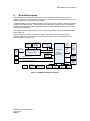
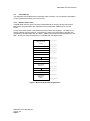
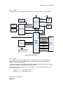
The ADM-XRC-5TZ follows the architecture of the ADM-XRC series and decouples the
“target” FPGA from the PCI interface, allowing user applications to be designed with minimum
effort and without the complexity of PCI design.
A separate Bridge / Control FPGA interfaces to the PCI bus and provides a simpler Local Bus
interface to the target FPGA. It also performs all of the board control functions including the
configuration of the target FPGA, programmable clock setup and the monitoring of on-board
voltage and temperature.
ZBT SRAM and serial flash memory connect to the target FPGA and are supported by Alpha
Data or Xilinx IP.
IO functionality is provided using XRM modules. MGT links are connected through a
SAMTEC QSE-DP connector, CN2. Remaining signals are connected through a 180 pin
SAMTEC QSH connector, CN1.
Config Flash
Memory
(32MB)
Bridge
Config
Pn1
Pn2
Pn3
PCI-X /
PCI64/66
User FPGA
Bridge / Control FPGA
(Virtex4 LX25)
Local Bus (32 bit)
Serial Flash
(4MB)
Pn4
Rear I/O (6 bit)
Pn15
XMC
PCIe / Serial RapidIO (x8)
JTAG
XRM
Bus
(146 bit)
Programmable
Clocks
System
Monitor
(LM87)
Virtex5
LXT/SXT/FXT
(FFG1738)
ZBT
SRAM
8MB
ZBT
SRAM
8MB
Power
Conversion
ZBT
SRAM
8MB
ZBT
SRAM
8MB
Figure 1 ADM-XRC-5TZ Block Diagram
ADM-XRC-5TZ User Manual
Version 2.0
Page 4
Front
MGT
(x8)
Front
I/O
CN1
(XRM)
ZBT
SRAM
8MB
ZBT
SRAM
8MB