1
21-S3-C7335/P7335-1199
USER'S MANUAL
S3C7335/P7335
4-Bit CMOS
Microcontroller
Revision 1
S3C7335/P7335
4-BIT CMOS
MICROCONTROLLER
USER'S MANUAL
Revision 1
Important Notice
The information in this publication has been carefully
checked and is believed to be entirely accurate at the
time of publication. Samsung assumes no
responsibility, however, for possible errors or
omissions, or for any consequences resulting from the
use of the information contained herein.
Samsung reserves the right to make changes in its
products or product specifications with the intent to
improve function or design at any time and without
notice and is not required to update this
documentation to reflect such changes.
This publication does not convey to a purchaser of
semiconductor devices described herein any license
under the patent rights of Samsung or others.
Samsung makes no warranty, representation, or
guarantee regarding the suitability of its products for
any particular purpose, nor does Samsung assume
any liability arising out of the application or use of any
product or circuit and specifically disclaims any and
all liability, including without limitation any
consequential or incidental damages.
applications. All operating parameters, including
"Typicals" must be validated for each customer
application by the customer's technical experts.
Samsung products are not designed, intended, or
authorized for use as components in systems
intended for surgical implant into the body, for other
applications intended to support or sustain life, or for
any other application in which the failure of the
Samsung product could create a situation where
personal injury or death may occur.
Should the Buyer purchase or use a Samsung
product for any such unintended or unauthorized
application, the Buyer shall indemnify and hold
Samsung and its officers, employees, subsidiaries,
affiliates, and distributors harmless against all claims,
costs, damages, expenses, and reasonable attorney
fees arising out of, either directly or indirectly, any
claim of personal injury or death that may be
associated with such unintended or unauthorized use,
even if such claim alleges that Samsung was
negligent regarding the design or manufacture of said
product.
"Typical" parameters can and do vary in different
S3C7335/P7335 4-Bit CMOS Microcontroller
User's Manual, Revision 0
Publication Number: 21-S3-C7335/P7335-1199
© 1999 Samsung Electronics
All rights reserved. No part of this publication may be reproduced, stored in a retrieval system, or transmitted in any
form or by any means, electric or mechanical, by photocopying, recording, or otherwise, without the prior written
consent of Samsung Electronics.
Samsung Electronics' Microcontroller Business has been awarded full ISO14001
certification (BVQ1 Certificate No. FM9330). All semiconductor products are
developed and manufactured in accordance with the highest quality standards and
objectives.
Samsung Electronics Co., Ltd.
San #24 Nongseo-Lee, Kiheung-Si
Yongin-City, Kyungi-Do, Korea
C.P.O. Box #37, Suwon 449-900
TEL:
FAX:
(0331) 209-6526, (02) 760-6526
(0331) 209-6547
H.P.: www.samsungsemi.com
Printed in the Republic of Korea
Preface
The S3C7335 User's Manual is designed specifically for application designers and programmers who are using
Samsung's S3C7335 microcontroller for product development. The manual is divided into two parts:
Part I
Part II
Programmer's Reference
Hardware Descriptions
Part I, 'Programmer's Reference,' contains software-related information to familiarize programmers with the
microcontroller's architecture, programming model, and instruction set. Part I has five Chapters:
Chapter 1
Chapter 2
Chapter 3
Product Overview
Address Spaces
Addressing Modes
Chapter 4
Chapter 5
Memory Map
SAM47 Instruction Set
Chapter 1, 'Product Overview,' is a high-level introduction to the S3C7335, ranging from a general product description
to detailed information about pin characteristics and circuit types.
Chapter 2, 'Address Spaces,’ introduces you to the S3C7335 programming model: the program memory (ROM) and
data memory (RAM) structures and how to address them. Chapter 2 also includes information about stack
operations, CPU registers, and the bit sequential carrier (BSC) register.
Chapter 3, 'Addressing Modes,' describes types of addressing supported by the SAM47 instruction set (direct,
indirect, and bit manipulation) and the addressing modes which are supported (1-bit, 4-bit, and 8-bit). Numerous
programming examples make the information practical and usable.
Chapter 4, 'Memory Map,' contains a detailed map of the addressable peripheral hardware registers in the memorymapped area of the RAM (bank 15). Chapter 4 also contains detailed descriptions in standard format of the most
commonly used hardware registers. These easy-to-read register descriptions can be used as a quick-reference
source when writing programs.
Chapter 5, 'Instruction Set,' first introduces the basic features and conventions of the SAM47 instruction set. Then,
two summary tables orient you to the individual instructions: One is a high-level summary of the most important
information about each instruction; the other is designed to give expert programmers a summary of binary code and
instruction notation information. The final part of Chapter 5 contains detailed descriptions of each instruction in a
standard format. Each instruction description includes one or more practical examples.
A basic familiarity with the information in Part I will make it easier for you to understand the hardware descriptions in
Part II. If you are unfamiliar with the SAM47 product family and are reading this user's manual for the first time, we
recommend that you read Chapters 1–3 carefully, and just scan the detailed information in Chapters 4 and 5 very
briefly. Later, you can refer back to Chapters 4 and 5 as necessary.
Part II "hardware Descriptions," has detailed information about specific hardware components of the S3C7335/P3316
microcontroller. Also included in Part II are electrical, mechanical, OTP, and development tools data. Part II has 13
Chapters:
Chapter 6
Chapter 7
Chapter 8
Chapter 9
Chapter 10
Chapter 11
Chapter 12
Chapter 13
Oscillator Circuits
Interrupts
Power-Down
RESET
I/O Ports
Timers and Timer/Counter
LCD Controller/Driver
A/D Converter
Chapter 14
Chapter 15
Chapter 16
Chapter 17
Chapter 18
Chapter 19
Chapter 20
Serial I/O Interface
PLL Frequency Synthesizer
Intermediate Frequency Counter
Electrical Data
Mechanical Data
KS57P3316 OTP
Development Tools
Two order forms are included at the back of this manual to facilitate customer order for S3C7335 microcontrollers:
the Mask ROM Order Form, and the Mask Option Selection Form. You can photocopy these forms, fill them out,
and then forward them to your local Samsung Sales Representative.
KS57C3316/P3316 MICROCONTROLLER
iii
Table of Contents
Part I — Programmer's Reference
Chapter 1
Product Overview
Overview .............................................................................................................................................1-1
OTP ...................................................................................................................................................1-1
Features .............................................................................................................................................1-2
Block Diagram ....................................................................................................................................1-4
Pin Assignments.................................................................................................................................1-5
Pin Descriptions ..................................................................................................................................1-6
Pin Circuit Diagrams............................................................................................................................1-9
Chapter 2
Address Spaces
Program Memory (ROM) ......................................................................................................................2-1
Overview .....................................................................................................................................2-1
General-Purpose Memory Areas ...................................................................................................2-2
Vector Address Area ...................................................................................................................2-2
Instruction Reference Area ...........................................................................................................2-4
Data Memory (RAM)............................................................................................................................2-5
Overview .....................................................................................................................................2-5
Working Registers .......................................................................................................................2-8
Stack Operations ................................................................................................................................2-12
Stack Pointer (SP) ......................................................................................................................2-12
Push Operations .........................................................................................................................2-13
Pop Operations ...........................................................................................................................2-14
Bit Sequential Carrier (BSC) Buffer........................................................................................................2-15
Program Counter (PC)..........................................................................................................................2-16
Program Status Word (PSW) ...............................................................................................................2-16
Interrupt Status Flags (IS0, IS1)....................................................................................................2-17
EMB Flag (EMB).........................................................................................................................2-18
ERB Flag (ERB)..........................................................................................................................2-19
Skip Condition Flags (SC2, SC1, SC0)..........................................................................................2-20
Carry Flag (C) .............................................................................................................................2-20
KS57C3316/P3316 MICROCONTROLLER
v
Table of Contents (Continued)
Chapter 3
Addressing Modes
Overview .............................................................................................................................................3-1
EMB and ERB Initialization Values .......................................................................................................3-3
Enable Memory Bank Settings .............................................................................................................3-4
Select Bank Register (SB) ...................................................................................................................3-5
Direct and Indirect Addressing ..............................................................................................................3-6
1-Bit Addressing..................................................................................................................................3-6
4-Bit Addressing..................................................................................................................................3-8
8-Bit Addressing..................................................................................................................................3-10
Chapter 4
Memory Map
Overview .............................................................................................................................................4-1
I/O Map for Hardware Registers ............................................................................................................4-1
Register Descriptions...........................................................................................................................4-6
Chapter 5
SAM47 Instruction Set
Overview .............................................................................................................................................5-1
Instruction Set Features .......................................................................................................................5-1
Symbols and Conventions ....................................................................................................................5-6
Opcode Definitions ..............................................................................................................................5-7
Calculating Additional Machine Cycles for Skips ....................................................................................5-7
High-Level Summary ............................................................................................................................5-8
Binary Code Summary .........................................................................................................................5-13
Instruction Descriptions........................................................................................................................5-23
vi
KS57C3316/P3316 MICROCONTROLLER
Table of Contents
(Continued)
Part II — Hardware Descriptions
Chapter 6
Oscillator Circuits
Overview .............................................................................................................................................6-1
Main System Oscillator Circuits............................................................................................................6-4
Subsystem Oscillator Circuits ..............................................................................................................6-4
Power Control Register (PCON) ............................................................................................................6-5
Instruction Cycle Times........................................................................................................................6-6
System Clock Mode Register (SCMOD) ................................................................................................6-7
Switching the CPU Clock .....................................................................................................................6-10
Clock Output Mode Register (CLMOD) ..................................................................................................6-12
Clock Output Circuit ............................................................................................................................6-13
Clock Output Procedure.......................................................................................................................6-13
Chapter 7
Interrupts
Overview .............................................................................................................................................7-1
Multiple Interrupts................................................................................................................................7-5
Interrupt Priority Register (IPR) .............................................................................................................7-7
External Interrupt 0 and 1 Mode Registers (IMOD0 and IMOD1) ...............................................................7-8
External Interrupt 2 Mode Register (IMOD2) ...........................................................................................7-10
Interrupt Flags .....................................................................................................................................7-12
Chapter 8
Power-Down
Overview .............................................................................................................................................8-1
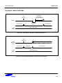
Idle Mode Timing Diagrams ..................................................................................................................8-3
Stop Mode Timing Diagrams.................................................................................................................8-4
Port Pin Configuration for Power-Down Mode..........................................................................................8-6
Recommended Connections for Unused Pins .........................................................................................8-7
Chapter 9
RESET
Overview .............................................................................................................................................9-1
Hardware Register Values after a System RESET..................................................................................9-3
KS57C3316/P3316 MICROCONTROLLER
vii
Table of Contents
Chapter 10
(Continued)
I/O Ports
Overview .............................................................................................................................................10-1
Port Mode Flags (PM FLAGS)..............................................................................................................10-3
Pull-Up Resistor Mode Register (PUMOD) .............................................................................................10-4
ADC and Port Control Register (APCON)...............................................................................................10-5
N-Channel Open-Drain Mode Register (PNE)..........................................................................................10-5
Pin Addressing for Output Port 7-13 ......................................................................................................10-6
Port 0 Circuit Diagram..........................................................................................................................10-7
Port 1 Circuit Diagram..........................................................................................................................10-8
Ports 2, 3 Circuit Diagram ....................................................................................................................10-9
Port 4 Circuit Diagram..........................................................................................................................10-10
Port 5 Circuit Diagram..........................................................................................................................10-11
Port 6 Circuit Diagram..........................................................................................................................10-12
Chapter 11
Timers and T imer/Counter
Overview .............................................................................................................................................11-1
Basic Timer (BT) .................................................................................................................................11-2
Overview .....................................................................................................................................11-2
Basic Timer Mode Register (BMOD)..............................................................................................11-4
Basic Timer Counter (BCNT).........................................................................................................11-5
Timer Output Enable Register (TOE) .............................................................................................11-5
Basic Timer Operation Sequence..................................................................................................11-5
Watchdog Timer Mode Register (WDMOD)....................................................................................11-7
Watchdog Timer Counter (WDCNT) ...............................................................................................11-7
Watchdog Timer Counter Clear Flag (WDTCF) ...............................................................................11-7
8-Bit Timer/Counter (TC0)....................................................................................................................11-9
Overview .....................................................................................................................................11-9
TC0 Function Summary ...............................................................................................................11-9
TC0 Component Summary ...........................................................................................................11-10
TC0 Programmable Timer/Counter Function ...................................................................................11-12
TC0 Operation Sequence .............................................................................................................11-12
TC0 Event Counter Function .........................................................................................................11-13
TC0 Clock Frequency Output........................................................................................................11-14
TC0 Serial I/O Clock Generation ...................................................................................................11-15
TC0 External Input Signal Divider ..................................................................................................11-15
TC0 Mode Register (TMOD0)........................................................................................................11-16
TC0 Counter Register (TCNT0)......................................................................................................11-18
TC0 Reference Register (TREF0) ..................................................................................................11-19
Watch Timer .......................................................................................................................................11-21
Overview .....................................................................................................................................11-21
Watch Timer Mode Register (WMOD) ...........................................................................................11-24
viii
KS57C3316/P3316 MICROCONTROLLER
Table of Contents
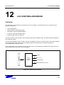
Chapter 12
(Continued)
LCD Controller/Driver
Overview .............................................................................................................................................12-1
LCD Circuit Diagram ............................................................................................................................12-2
LCD RAM Address Area ......................................................................................................................12-3
LCD Control Register (LCON) ...............................................................................................................12-4
LCD Mode Register (LMOD) .................................................................................................................12-5
LCD Port Control Register (LPOT) .........................................................................................................12-6
LCD Drive Voltage ...............................................................................................................................12-7
LCD Voltage Dividing Resistors.............................................................................................................12-7
Common (COM) Signals ......................................................................................................................12-7
Segment (SEG) Signals.......................................................................................................................12-7
Chapter 13
A/D Converter
Overview .............................................................................................................................................13-1
ADC Data Register (ADATA) ................................................................................................................13-3
ADC Mode Register (ADMOD)..............................................................................................................13-3
ADC and Port Control Register (APCON)...............................................................................................13-3
ADC Control Register (AFLAG).............................................................................................................13-4
Digital-to-Analog Converter (DAC) Block ................................................................................................13-4
Conversion Timing ...............................................................................................................................13-4
ADC Procedure Description..................................................................................................................13-5
Chapter 14
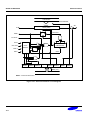
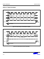
Serial I/O Interface
Overview .............................................................................................................................................14-1
SIO Operation Sequence......................................................................................................................14-1
Serial I/O Mode Register (SMOD) .........................................................................................................14-3
Serial I/O Timing Diagrams...................................................................................................................14-4
Serial I/O Buffer Register (SBUF) ..........................................................................................................14-5
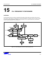
Chapter 15
PLL Frequency Synthesizer
Overview .............................................................................................................................................15-1
PLL Frequency Synthesizer Function....................................................................................................15-2
PLL Data Register (PLLD) ....................................................................................................................15-3
Reference Frequency Generator............................................................................................................15-4
PLL Mode Register (PLMOD) ...............................................................................................................15-5
PLL Reference Frequency Selection Register (PLLREF) .........................................................................15-6
Phase Detector, Charge Pump, and Unlock Detector..............................................................................15-6
Using the PLL Frequency Synthesizer...................................................................................................15-8
KS57C3316/P3316 MICROCONTROLLER
ix
Table of Contents
Chapter 16
(Concluded)
Intermediate Frequency Counter
Overview .............................................................................................................................................16-1
IFC Mode Register (IFMOD) .................................................................................................................16-2
PLL Flag Register (PLLREG)................................................................................................................16-2
Gate Times .........................................................................................................................................16-3
IF Counter (IFC) Operation....................................................................................................................16-6
Input Pin Configuration .........................................................................................................................16-7
IFC Data Calculation............................................................................................................................16-8
Chapter 17
Electrical Data
Overview .............................................................................................................................................17-1
Timing Waveforms ...............................................................................................................................17-12
Chapter 18
Mechanical Data
Overview .............................................................................................................................................18-1
Chapter 19
KS57P3316 OTP
Overview .............................................................................................................................................19-1
Operating Mode Characteristics............................................................................................................19-3
Timing Waveforms ...............................................................................................................................19-13
Chapter 20
Development Tools
Overview .............................................................................................................................................20-1
SHINE ........................................................................................................................................20-1
SAMA Assembler........................................................................................................................20-1
SASM57.....................................................................................................................................20-1
HEX2ROM ..................................................................................................................................20-1
Target Boards .............................................................................................................................20-1
OTPs .........................................................................................................................................20-1
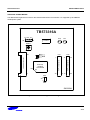
TB573316A Target Board .............................................................................................................20-3
Idle LED .....................................................................................................................................20-5
Stop LED....................................................................................................................................20-5
x
KS57C3316/P3316 MICROCONTROLLER
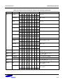
List of Figures
Figure
Number
Title
Page
Number
1-1
1-2
1-3
1-4
1-5
1-6
1-7
1-8
1-9
1-10
1-11
1-12
1-13
1-14
1-15
1-16
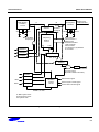
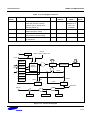
S3C7335 Simplified Block Diagram ...................................................................................1-4
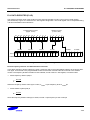
S3C7335 80-QFP Pin Assignment ....................................................................................1-5
Pin Circuit Type A ...........................................................................................................1-9
Pin Circuit Type A-2(EO)..................................................................................................1-9
Pin Circuit Type A-4 (P1)..................................................................................................1-9
Pin Circuit Type B (RESET) .............................................................................................1-9
Pin Circuit Type B-4.........................................................................................................1-9
Pin Circuit Type B-5(CE)..................................................................................................1-9
Pin Circuit Type C ...........................................................................................................1-10
Pin Circuit Type D-2.........................................................................................................1-10
Pin Circuit Type D-4.........................................................................................................1-10
Pin Circuit Type D-7 (P6)..................................................................................................1-10
Pin Circuit Type F-10 (P5) ................................................................................................1-11
Pin Circuit Type H (COM0-COM3).....................................................................................1-11
Pin Circuit Type H-4.........................................................................................................1-11
Pin Circuit Type H-28 (P7-P13) .........................................................................................1-11
2-1
2-2
2-3
2-4
2-5
2-6
2-7
2-8
ROM Address Structure...................................................................................................2-2
Vector Address Structure.................................................................................................2-2
Data Memory (RAM) Map.................................................................................................2-5
Working Register Map .....................................................................................................2-8
Register Pair Configuration ...............................................................................................2-9
1-Bit, 4-Bit, and 8-Bit Accumulator....................................................................................2-10
Push-Type Stack Operations ............................................................................................2-13
Pop-Type Stack Operations..............................................................................................2-14
3-1
3-2
RAM Address Structure ...................................................................................................3-2
SMB and SRB Values in the SB Register..........................................................................3-5
4-1
Register Description Format .............................................................................................4-7
6-1
6-2
6-3
6-4
6-5
6-6
Clock Circuit Diagram ......................................................................................................6-3
Crystal/Ceramic Oscillator................................................................................................6-4
External Oscillator...........................................................................................................6-4
Crystal/Ceramic Oscillator...............................................................................................6-4
External Oscillator...........................................................................................................6-4
CLO Output Pin Circuit Diagram .......................................................................................6-13
KS57C3316/P3316 MICROCONTROLLER
xi
List of Figures (Continued)
Figure
Number
Title
Page
Number
7-1
7-2
7-3
7-4
7-5
7-6
Interrupt Execution Flowchart ...........................................................................................7-3
Interrupt Control Circuit Diagram .......................................................................................7-4
Two-Level Interrupt Handling .............................................................................................7-5
Multi-Level Interrupt Handling ............................................................................................7-6
Circuit Diagram for INT0 and INT1 Pins ..............................................................................7-9
Circuit Diagram for INT2 ...................................................................................................7-11
8-1
8-2
8-3
8-4
8-5
Timing When Idle Mode is Released by RESET .................................................................8-3
Timing When Idle Mode is Released by an Interrupt ............................................................8-3
Timing When Stop Mode is Released by RESET ...............................................................8-4
Timing When Stop Mode is Release by an Interrupt ............................................................8-4
Timing When CE Low Mode is Release by CE rising edge ..................................................8-4
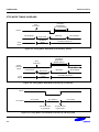
9-1
9-2
Reset Operation by RESET Pin.......................................................................................9-2
Reset Operation by CE Pin ..............................................................................................9-2
10-1
10-2
10-3
10-4
10-5
10-6
Port 0 Circuit Diagram......................................................................................................10-7
Port 1 Circuit Diagram......................................................................................................10-8
Ports 2, 3 Circuit Diagram ................................................................................................10-9
Port 4 Circuit Diagram......................................................................................................10-10
Port 5 Circuit Diagram......................................................................................................10-11
Port 6 Circuit Diagram......................................................................................................10-12
11-1
11-2
11-3
11-4
Basic Timer Circuit Diagram .............................................................................................11-3
TC0 Circuit Diagram.........................................................................................................11-11
TC0 Timing Diagram ........................................................................................................11-18
Watch Timer Circuit Diagram............................................................................................11-23
12-1
12-2
12-3
12-4
12-5
12-6
12-7
12-8
12-9
12-10
12-11
12-12
12-13
LCD Function Diagram.....................................................................................................12-1
LCD Circuit Diagram ........................................................................................................12-2
LCD Display Data RAM Organization ................................................................................12-3
Voltage Dividing Resistor Circuit Diagrams.........................................................................12-8
LCD Signal Waveforms in Static Mode .............................................................................12-9
LCD Connection Example in Static Mode ..........................................................................12-10
LCD Signal Waveforms at 1/2 Duty, 1/2 Bias .....................................................................12-11
LCD Connection Example at 1/2 Duty, 1/2 Bias .................................................................12-12
LCD Signal Waveforms at 1/3 Duty, 1/2 Bias .....................................................................12-13
LCD Signal Waveforms at 1/3 Duty, 1/3 Bias .....................................................................12-14
LCD Connection Example at 1/3 Duty, 1/3 Bias .................................................................12-15
LCD Signal Waveforms at 1/4 Duty, 1/3 Bias .....................................................................12-16
LCD Connection Example at 1/4 Duty, 1/3 Bias .................................................................12-17
xii
KS57C3316/P3316 MICROCONTROLLER
List of Figures (Concluded)
Figure
Number
Title
Page
Number
13-1
13-2
A/D Converter Circuit Diagram ..........................................................................................13-2
A/D Converter Timing Diagram ..........................................................................................13-5
14-1
14-2
14-3
Serial I/O Interface Circuit Diagram....................................................................................14-2
SIO Timing in Transmit/Receive Mode ...............................................................................14-4
SIO Timing in Receive-Only Mode .....................................................................................14-4
15-1
15-2
15-3
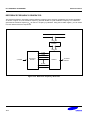
Block Diagram of the PLL Frequency synthesizer...............................................................15-1
PLL Register Configuration ...............................................................................................15-3
Reference Frequency Generator........................................................................................15-4
16-1
16-2
16-3
16-4
16-5
IF Counter Block Diagram ................................................................................................16-1
Gate Timing (1,4, or 8 ms)................................................................................................16-3
Gate Timing (When Open)................................................................................................16-4
Gate Timing (1-ms Error)..................................................................................................16-5
AMIF and FMIF Pin Configuration......................................................................................16-7
17-1
17-2
17-3
17-4
Standard Operating Voltage Range ...................................................................................17-11
Stop Mode Release Timing When Initiated by RESET ........................................................17-12
Stop Mode Release Timing When Initiated by an Interrupt Request ......................................17-12
A.C. Timing Measurement Points (Except for XIN and XTIN)..................................................17-13
17-5
17-6
Clock Timing Measurement at XIN .....................................................................................17-13
Clock Timing Measurement at XT IN....................................................................................17-13
17-7
17-8
Input Timing for RESET Signal..........................................................................................17-14
Input Timing for External Interrupts and Quasi-Interrupts......................................................17-14
18-1
80-QFP-1420C Package Dimensions ................................................................................18-1
19-1
19-2
19-3
19-4
19-5
KS57P3316 Pin Assignments (80-QFP) ............................................................................19-2
Standard Operating Voltage Range ...................................................................................19-12
Stop Mode Release Timing When Initiated by RESET ........................................................19-13
Stop Mode Release Timing When Initiated by an Interrupt Request ......................................19-13
A.C. Timing Measurement Points (Except for XIN and XTIN)..................................................19-14
19-6
19-7
Clock Timing Measurement at XIN .....................................................................................19-14
Clock Timing Measurement at XT IN....................................................................................19-14
19-8
19-9
Input Timing for RESET Signal..........................................................................................19-15
Input Timing for External Interrupts and Quasi-Interrupts......................................................19-15
20-1
20-2
20-3
20-4
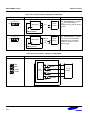
SMDS Product Configuration (SMDS2+)............................................................................20-2
TB573316A Target Board Configuration..............................................................................20-3
40-Pin Connectors for TB573316A.....................................................................................20-6
TB573316A Adapter Cable for 80-QFP Package (S3C7335).................................................20-6
KS57C3316/P3316 MICROCONTROLLER
xiii
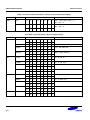
List of Tables
Table
Number
Title
Page
Number
1-1
S3C7335/P3316 Pin Descriptions .....................................................................................1-6
2-1
2-2
2-3
2-4
2-5
2-6
2-7
Program Memory Address Ranges....................................................................................2-1
Data Memory Organization and Addressing .......................................................................2-7
Working Register Organization and Addressing..................................................................2-9
BSC Register Organization...............................................................................................2-15
Program Status Word Bit Descriptions ..............................................................................2-16
Interrupt Status Flag Bit Settings ......................................................................................2-17
Valid Carry Flag Manipulation Instructions .........................................................................2-20
3-1
3-2
3-3
3-4
RAM Addressing Not Affected by the EMB Value...............................................................3-4
1-Bit Direct and Indirect RAM Addressing ..........................................................................3-6
4-Bit Direct and Indirect RAM Addressing ..........................................................................3-8
8-Bit Direct and Indirect RAM Addressing ..........................................................................3-10
4-1
I/O Map for Memory Bank 15............................................................................................4-2
5-1
5-2
5-3
5-4
5-5
5-6
5-7
5-8
5-9
5-10
5-11
5-12
5-13
5-14
5-15
5-16
5-17
5-18
5-19
5-20
Valid 1-Byte Instruction Combinations for REF Look-Ups ....................................................5-2
Bit Addressing Modes and Parameters..............................................................................5-4
Skip Conditions for ADC and SBC Instructions ...................................................................5-5
Data Type Symbols .........................................................................................................5-6
Register Identifiers ...........................................................................................................5-6
Instruction Operand Notation ............................................................................................5-6
Opcode Definitions (Direct)...............................................................................................5-7
Opcode Definitions (Indirect).............................................................................................5-7
CPU Control Instructions - High-Level Summary .................................................................5-9
Program Control Instructions - High-Level Summary............................................................5-9
Data Transfer Instructions - High-Level Summary ................................................................5-10
Logic Instructions - High-Level Summary ...........................................................................5-11
Arithmetic Instructions - High-Level Summary ....................................................................5-11
Bit Manipulation Instructions -High-Level Summary .............................................................5-12
CPU Control Instructions - Binary Code Summary ..............................................................5-14
Program Control Instructions - Binary Code Summary.........................................................5-15
Data Transfer Instructions - Binary Code Summary .............................................................5-16
Logic Instructions - Binary Code Summary ........................................................................5-18
Arithmetic Instructions - Binary Code Summary .................................................................5-19
Bit Manipulation Instructions - Binary Code Summary .........................................................5-20
KS57C3316/P3316 MICROCONTROLLER
xv
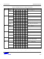
List of Tables (Continued)
Table
Number
Title
Page
Number
6-1
6-2
6-3
6-4
6-5
6-6
6-7
Power Control Register (PCON) Organization.....................................................................6-5
Instruction Cycle Times for CPU Clock Rates.....................................................................6-6
System Clock Mode Register (SCMOD) Organization.........................................................6-7
Main or Sub Oscillation Stop Mode ...................................................................................6-8
System Operating Mode Comparison ................................................................................6-9
Elapsed Machine Cycles During CPU Clock Switch............................................................6-11
Clock Output Mode Register (CLMOD) Organization...........................................................6-12
7-1
7-2
7-3
7-4
7-5
7-6
7-7
7-8
Interrupt Types and Corresponding Port Pin(s)....................................................................7-1
IS1 and IS0 Bit Manipulation for Multi-Level Interrupt Handling..............................................7-6
Standard Interrupt Priorities ..............................................................................................7-7
Interrupt Priority Register Settings.....................................................................................7-7
IMOD0, 1 and 2 Register Organization...............................................................................7-8
IMOD2 Register Bit Settings.............................................................................................7-10
Interrupt Enable and Interrupt Request Flag Addresses .......................................................7-12
Interrupt Request Flag Conditions and Priorities .................................................................7-13
8-1
8-2
Hardware Operation During Power-Down Modes .................................................................8-2
Unused Pin Connections for Reducing Power Consumption.................................................8-7
9-1
Hardware Register Values After a System Reset ................................................................9-3
10-1
10-2
10-3
10-4
10-5
10-6
I/O Port Overview.............................................................................................................10-2
Port Pin Status During Instruction Execution......................................................................10-2
Port Mode Group Flags ....................................................................................................10-3
Pull-Up Resistor Mode Register (PUMOD) Organization......................................................10-4
N-Channel Open Drain Mode Register (PNE) Setting ..........................................................10-5
LPOT Setting for Port 7-13 Output Control .........................................................................10-6
11-1
11-2
11-3
11-4
11-5
11-6
11-7
11-8
Basic Timer Register Overview..........................................................................................11-3
Basic Timer Mode Register (BMOD) Organization ..............................................................11-4
Watchdog Timer Interval Time...........................................................................................11-7
TC0 Register Overview .....................................................................................................11-11
TMOD0 Setting for TCL0 Edge Detection ...........................................................................11-13
Timer 0 Mode Register Organization..................................................................................11-16
TMOD0.6,TMOD0.5 and TMOD0.4 Bit Settings ..................................................................11-17
Watch Timer Mode Register (WMOD) Organization ............................................................11-24
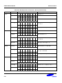
12-1
12-2
12-3
12-4
12-5
12-6
12-7
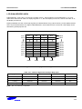
Common Signal Pins Used per Duty Cycle ........................................................................12-3
LCD Control Register (LCON) Organization ........................................................................12-4
LCON.0 and LMOD.3 Bit Settings .....................................................................................12-4
LCD Mode Register (LMOD) Organization..........................................................................12-5
LCD Clock Signal (LCDCK) and Frame Frequency..............................................................12-6
LCD Port Control Register Setting.....................................................................................12-6
LCD Drive Voltage Values ................................................................................................12-7
xvi
KS57C3316/P3316 MICROCONTROLLER
List of Tables
Table
Number
Title
(Concluded)
Page
Number
13-1
13-2
13-3
A/D Converter Component Overview...................................................................................13-2
A/D Converter Mode Register Settings...............................................................................13-3
A/D Converter Control Flag Settings ..................................................................................13-4
14-1
SIO Mode Register (SMOD) Organization ..........................................................................14-3
15-1
15-2
PLMOD Organization.......................................................................................................15-5
PLLREF Register Organization .........................................................................................15-6
16-1
16-2
IFMOD Organization ........................................................................................................16-2
IF Counter Frequency Characteristics................................................................................16-6
17-1
17-2
17-3
17-4
17-5
17-6
17-7
Absolute Maximum Ratings..............................................................................................17-2
D.C. Electrical Characteristics..........................................................................................17-3
Main System Clock Oscillator Characteristics....................................................................17-6
Subsystem Clock Oscillator Characteristics ......................................................................17-7
Input/Output Capacitance.................................................................................................17-8
A.C. Electrical Characteristics..........................................................................................17-8
RAM Data Retention Supply Voltage in Stop Mode.............................................................17-11
19-1
19-2
19-3
19-4
19-5
19-6
19-7
19-8
19-9
Pin Descriptions Used to Read/Write the EPROM..............................................................19-3
Comparison of KS57P3316 and S3C7335 Features ............................................................19-3
Operating Mode Selection Criteria.....................................................................................19-3
D.C. Electrical Characteristics..........................................................................................19-4
Main System Clock Oscillator Characteristics....................................................................19-7
Subsystem Clock Oscillator Characteristics ......................................................................19-8
Input/Output Capacitance.................................................................................................19-9
A.C. Electrical Characteristics..........................................................................................19-9
RAM Data Retention Supply Voltage in Stop Mode.............................................................19-12
20-1
20-2
20-3
Power Selection Settings for TB573316A ...........................................................................20-4
Pin Selection Settings for TB573316A ...............................................................................20-4
Sub-clock Selection Settings for TB573316A .....................................................................20-5
KS57C3316/P3316 MICROCONTROLLER
xvii
List of Programming Tips
Description
Page
Number
Chapter 2: Address Spaces
Defining Vectored Interrupts..................................................................................................................2-3
Using the REF Look-Up Table...............................................................................................................2-4
Clearing Data Memory Banks 0 and 1 ...................................................................................................2-7
Selecting the Working Register Area.....................................................................................................2-11
Initializing the Stack Pointer .................................................................................................................2-12
Using the BSC Register to Output 16-Bit Data .......................................................................................2-15
Setting ISx Flags for Interrupt Processing ..............................................................................................2-17
Using the EMB Flag to Select Memory Banks .......................................................................................2-18
Using the ERB Flag to Select Register Banks........................................................................................2-19
Using the Carry Flag as a 1-Bit Accumulator..........................................................................................2-21
Chapter 3: Addressing Modes
Initializing the EMB and ERB Flags.......................................................................................................3-3
1-Bit Addressing Modes .......................................................................................................................3-7
4-Bit Addressing Modes .......................................................................................................................3-8
8-Bit Addressing Modes .......................................................................................................................3-11
Chapter 5: SAM47 Instruction Set
Example of the Instruction Redundancy Effect........................................................................................5-3
Chapter 6: Oscillator Circuits
Setting the CPU Clock.........................................................................................................................6-6
Switching Between Main System and Subsystem Clock.........................................................................6-11
CPU Clock Output to the CLO Pin ........................................................................................................6-13
Chapter 7: Interrupts
Setting the INT Interrupt Priority ............................................................................................................7-8
Using the INT2 as Key Input Interrupt ....................................................................................................7-10
Setting the INT Interrupt Priority ............................................................................................................7-14
Chapter 8: Power Down
Reducing Power Consumption for Key Input Interrupt Processing.............................................................8-5
KS57C3316/P3316 MICROCONTROLLER
xix
List of Programming Tips (Concluded)
Description
Page
Number
Chapter 10: I/O Ports
Configuring I/O Ports to Input or Output .................................................................................................10-3
Enabling and Disabling I/O Port Pull-Up Resistors ..................................................................................10-4
Chapter 11: Timers
Using the Basic Timer..........................................................................................................................11-6
Using the Watchdog Timer ...................................................................................................................11-8
TC0 Signal Output to the TCLO0 Pin .....................................................................................................11-14
External TCL0 Clock Output to the TCLO0 Pin .......................................................................................11-15
Restarting TC0 Counting Operation .......................................................................................................11-17
Setting a TC0 Timer Interval..................................................................................................................11-20
Using the Watch Timer ........................................................................................................................11-25
Chapter 13: A/D Converter
Configuring A/D Converter Input Pins .....................................................................................................13-6
Chapter 14: Serial I/O Interface
Setting Transmit/Receive Modes for Serial I/O........................................................................................14-5
Chapter 16: Intermediate Frequency Counter
Counting the Frequency at the FMIF pin (8-ms Gate Time)......................................................................16-7
xx
KS57C3316/P3316 MICROCONTROLLER
List of Register Descriptions
Register
Identifier
Full Register Name
Page
Number
ADMOD
ADC Mode Register.........................................................................................................4-8
AFLAG
ADC FLAG Register ........................................................................................................4-9
APCON
ADC and Port Control Register ........................................................................................4-10
BMOD
Basic Timer Mode Register ..............................................................................................4-11
CLMOD
Clock Output Mode Register.............................................................................................4-12
IE0, 1, IRQ0, 1 INT0, 1 Interrupt Enable/Request Flags..............................................................................4-13
IE2, IRQ2
INT2 Interrupt Enable/Request Flags .................................................................................4-14
IE4, IRQ4
INT4 Interrupt Enable/Request Flags ................................................................................4-15
IEB, IRQB
INTB Interrupt Enable/Request Flags .................................................................................4-15
IECE, IRQCE
INTCE Interrupt Enable/Request Flags...............................................................................4-16
IEIF, IRQIF
INTIF Interrupt Enable/Request Flags ................................................................................4-16
IES, IRQS
INTS Interrupt Enable/Request Flags .................................................................................4-17
IET0, IRQT0
INTT0 Interrupt Enable/Request Flags................................................................................4-18
IEW, IRQW
INTW Interrupt Enable/Request Flags ................................................................................4-19
IFMOD
IF Counter Mode Register.................................................................................................4-20
IMOD0
External Interrupt 0 (INT0) Mode Register...........................................................................4-21
IMOD1
External Interrupt 1 (INT1) Mode Register...........................................................................4-22
IMOD2
External Interrupt 2 (INT2) Mode Register...........................................................................4-23
IPR
Interrupt Priority Register..................................................................................................4-24
LCON
LCD Output Control Register ............................................................................................4-25
LMOD
LCD Mode Control Register ..............................................................................................4-26
LPOT
LCD Port Control Register ................................................................................................4-27
PCON
Power Control Register ....................................................................................................4-28
KS57C3316/P3316 MICROCONTROLLER
xxi
List of Register Descriptions
Register
Identifier
Full Register Name
Page
Number
PLLREF
PLL Reference Frequency Selection Register.....................................................................4-29
PLLREG
PLL Status Register ........................................................................................................4-30
PLMOD
PLL Mode Register..........................................................................................................4-31
PMG0
Port I/O Mode Control Register (Port 0) .............................................................................4-32
PMG1
Port I/O Mode Control Register (Port 2 and Port 3) .............................................................4-33
PMG2
Port I/O Mode Control Register (Port 4 and Port 5) .............................................................4-34
PMG3
Port I/O Mode Control Register (Port 6) .............................................................................4-35
PNE
Port Open-drain Enable Register.......................................................................................4-36
POFR
Power On Flag Register ...................................................................................................4-37
PSW
Program Status Word ......................................................................................................4-38
PUMOD
Pull-up Resistor Mode Register.........................................................................................4-39
SCMOD
System Clock Mode Control Register................................................................................4-40
SMOD
Serial I/O Mode Register ..................................................................................................4-41
TMOD0
Timer 0 Mode Register.....................................................................................................4-42
TOE
Timer Output Enable Register...........................................................................................4-43
WDFLAG
Watchdog Timer Counter Clear Flag Register.....................................................................4-44
WDMOD
Watchdog Timer Mode Register........................................................................................4-45
WMOD
Watch Timer Mode Register .............................................................................................4-46
xxii
KS57C3316/P3316 MICROCONTROLLER
List of Instruction Descriptions
Instruction
Mnemonic
Full Instruction Name
Page
Number
ADC
Add With Carry ...............................................................................................................5-24
ADS
Add And Skip On Overflow ...............................................................................................5-26
ADS
Add And Skip On Overflow ...............................................................................................5-27
AND
Logical And.....................................................................................................................5-28
BAND
Bit Logical And................................................................................................................5-29
BAND
Bit Logical And................................................................................................................5-30
BITR
Bit Reset ........................................................................................................................5-31
BITR
Bit Reset ........................................................................................................................5-32
BITS
Bit Set............................................................................................................................5-33
BITS
Bit Set............................................................................................................................5-34
BOR
Bit Logical OR.................................................................................................................5-35
BOR
Bit Logical OR.................................................................................................................5-36
BTSF
Bit Test and Skip on False...............................................................................................5-37
BTSF
Bit Test and Skip on False...............................................................................................5-38
BTST
Bit Test and Skip on True.................................................................................................5-39
BTST
Bit Test and Skip on True.................................................................................................5-40
BTSTZ
Bit Test and Skip on True; Clear Bit ..................................................................................5-41
BTSTZ
Bit Test and Skip on True; Clear Bit ..................................................................................5-42
BXOR
Bit Exclusive OR .............................................................................................................5-43
BXOR
Bit Exclusive OR .............................................................................................................5-44
CALL
Call Procedure ................................................................................................................5-45
CALLS
Call Procedure (Short)......................................................................................................5-46
CCF
Complement Carry Flag ...................................................................................................5-47
COM
Complement Accumulator ................................................................................................5-48
CPSE
Compare and Skip if Equal ...............................................................................................5-49
DECS
Decrement and Skip on Borrow.........................................................................................5-50
DI
Disable Interrupts ............................................................................................................5-51
EI
Enable Interrupts .............................................................................................................5-52
IDLE
Idle Operation..................................................................................................................5-53
INCS
Increment and Skip on Carry ............................................................................................5-54
IRET
Return From Interrupt .......................................................................................................5-55
JP
Jump..............................................................................................................................5-56
KS57C3316/P3316 MICROCONTROLLER
xxiii
JPS
Jump (Short)...................................................................................................................5-57
JR
Jump Relative (Very Short)...............................................................................................5-58
xxiv
KS57C3316/P3316 MICROCONTROLLER
List of Instruction Descriptions (Continued)
Instruction
Mnemonic
Full Instruction Name
Page
Number
JR
Jump Relative (Very Short)...............................................................................................5-59
LD
Load...............................................................................................................................5-60
LD
Load...............................................................................................................................5-61
LD
Load...............................................................................................................................5-62
LD
Load...............................................................................................................................5-63
LDB
Load Bit..........................................................................................................................5-64
LDB
Load Bit..........................................................................................................................5-65
LDC
Load Code Byte ..............................................................................................................5-66
LDC
Load Code Byte ..............................................................................................................5-67
LDD
Load Data Memory and Decrement ...................................................................................5-68
NOP
OR
No Operation...................................................................................................................5-70
Logical OR......................................................................................................................5-71
POP
Pop From Stack..............................................................................................................5-72
PUSH
Push Onto Stack.............................................................................................................5-73
RCF
Reset Carry Flag .............................................................................................................5-74
REF
Reference Instruction .......................................................................................................5-75
REF
Reference Instruction .......................................................................................................5-76
REF
Reference Instruction .......................................................................................................5-77
RET
Return From Subroutine ...................................................................................................5-78
RRC
Rotate Accumulator Right Through Carry ...........................................................................5-79
SBC
Subtract With Carry .........................................................................................................5-80
SBC
Subtract With Carry .........................................................................................................5-81
SBS
Subtract .........................................................................................................................5-82
SCF
Set Carry Flag.................................................................................................................5-83
SMB
Select Memory Bank .......................................................................................................5-84
SRB
Select Register Bank .......................................................................................................5-85
SRET
Return From Subroutine and Skip .....................................................................................5-86
STOP
Stop Operation................................................................................................................5-87
VENT
Load EMB, ERB, and Vector Address...............................................................................5-88
VENT
Load EMB, ERB, and Vector Address...............................................................................5-89
XCH
Exchange A or EA with Nibble or Byte ..............................................................................5-90
XCHD
Exchange and Decrement ................................................................................................5-91
KS57C3316/P3316 MICROCONTROLLER
xxv
XCHI
Exchange and Increment..................................................................................................5-92
XOR
Logical Exclusive OR.......................................................................................................5-93
xxvi
KS57C3316/P3316 MICROCONTROLLER
S3C7335/P7335
1
PRODUCT OVERVIEW
PRODUCT OVERVIEW
OVERVIEW
The S3C7335 single-chip CMOS microcontroller has been designed for high performance using Samsung's newest
4-bit CPU core, SAM47 (Samsung Arrangeable Microcontrollers).
With features such as LCD direct drive capability, 4-channel A/D converter, 8-bit timer/counter, watch timer and PLL
frequency synthesizer, it offers you an excellent design solution for a wide variety of applications that require LCD
functions and audio applications .
Up to 56 pins of the 80-pin QFP package, it can be dedicated to I/O. Eight vectored interrupts provide fast response
to internal and external events. In addition, the S3C7335's advanced CMOS technology provides for low power
consumption and a wide operating voltage range.
OTP
The S3C7335 microcontroller is also available in OTP (One Time Programmable) version, S3P7335. The S3P7335 6
microcontroller has an on-chip 16-Kbyte one-time-programmable EPROM instead of masked ROM. The S3P7335 6
is comparable to S3C7335, both in function and in pin configuration.
1-1
PRODUCT OVERVIEW
S3C7335/P7335
FEATURES
Memory
Watch Timer
•
512-nibble RAM
•
•
16K-byte ROM
Time interval generation
: 0.5 s, 3.9 ms at 32.768 kHz
•
Frequency outputs to BUZ pin
•
Clock source generation for LCD
I/O Pins
•
Input only: 4 pins
•
Output only: 28 pins
•
I/O: 24 pins
8-Bit Serial I/O Interface
•
8-bit transmit/receive mode
•
8-bit receive mode
LCD Controller/Driver
•
Data direction selectable (LSB-first or MSB-first)
•
Maximum 14-digit LCD direct drive capability
•
Internal or external clock source
•
28 segment x 4 common signals
•
Display modes: Static, 1/2 duty (1/2 bias)
1/3 duty (1/2 or 1/3 bias), 1/4 duty (1/3 bias)
A/D Converter
•
4-channels with 8-bit resolution
8-Bit Basic Timer
Bit Sequential Carrier Buffer
•
Programmable interval timer functions
•
•
Watch-dog timer function
Support 16-bit serial data transfer in arbitrary
format
PLL Frequency Synthesizer
8-Bit Timer/Counter
•
Level = 300 mVp-p (min)
•
Programmable 8-bit timer
•
AMVCO range = 0.5 MHz to 30 MHz
•
External event counter
•
FMVCO range = 30 MHz to 150 MHz
•
Arbitrary clock frequency output
•
External clock signal divider
•
Serial I/O interface clock generator
1-2
16-Bit Intermediate Frequency (IF) Counter
•
Level = 300 mVp-p (min)
•
AMIF range = 100 kHz to 1 MHz
•
FMIF range = 5 MHz to 15 MHz
KS57C3316/P3316 (Preliminary Spec)
PRODUCT OVERVIEW
FEATURES (Continued)
Interrupts
Instruction Execution Times
•
Four internal vectored interrupts
•
0.9, 1.8, 14.2 µs at 4.5 MHz
•
Four external vectored interrupts
•
122 µs at 32.768 kHz (subsystem)
•
Two quasi-interrupts
Operating Temperature
Memory-Mapped I/O Structure
•
•
– 25 °C to 85 °C
Data memory bank 15
Operating Voltage Range
Three Power-Down Modes
•
1.8 V to 5.5 V at 3MHz
•
Idle: Only CPU clock stops
•
PLL/IFC operation: 2.5V to 3.5V or 4.0V to 5.5V
•
Stop1: Main system or subsystem clock stops
•
Stop2: Main system and subsystem clock stop
•
CE low: PLL and IFC stop
Package Type
•
80-pin QFP
Oscillation Sources
•
Crystal or ceramic oscillator for main system
clock
•
Crystal for subsystem clock
•
Main system clock frequency: 4.5 MHz (Typ)
•
Subsystem clock frequency: 32.768 kHz (Typ)
•
CPU clock divider circuit (by 4, 8, or 64)
1-3
PRODUCT OVERVIEW
S3C7335/P7335
BLOCK DIAGRAM
P0.0/BTCO
P0.1/TCLO0
P0.2/TCL0
P0.3/BUZ
P1.0/INT0
P1.1/INT1
P1.2/INT2
P1.3/INT4
INT0-INT4
I/O Port 0
RESET
CE
XIN
XTIN
XOUT XTOUT
Basic
Timer
Watch
Timer
Timer/
Counter 0
Input Port 1
P2.0
P2.1
P2.2
P2.3
I/O Port 2
P3.0
P3.1
P3.2
P3.3
I/O Port 3
Serial
I/O Port
P4.0/ SCK
P4.1/SO
P4.2/SI
P4.3/CLO
I/O Port 4
P5.0/ADC0
P5.1/ADC1
P5.2/ADC2
P5.3/ADC3
I/O Port 5
A/D
Converter
Interrupt
Control
Block
Clock
Internal
Interrupts
Instruction Decoder
Arithmetic
and
Logic Unit
Instruction
Register
Program
Counter
Program
Status Word
Stack
Pointer
IF
Counter
PLL
Synthesizer
LCD Driver/
Controller
Output Port
11,12,13
Output Port
7,8,9,10
512 x 4-Bit
Data Memory
16K-Byte
Program Memory
I/O Port 6
Figure 1-1. S3C7335 Simplified Block Diagram
1-4
Watchdog
Timer
AMIF
FMIF
VCOAM
VCOFM
EO
BIAS
VLC0-VLC2
COM0-COM3
P13.0-P13.3
/SEG24-SEG27
P12.0-P12.3
/SEG20-SEG23
P11.0-P11.3
/SEG16-SEG19
P10.0-P10.3
/SEG12-SEG15
P9.0-P9.3
/SEG8-SEG11
P8.0-P8.3
/SEG4-SEG7
P7.0-P7.3
/SEG0-SEG3
P6.0-P6.3
KS0-KS3
KS57C3316/P3316 (Preliminary Spec)
PRODUCT OVERVIEW
PIN ASSIGNMENTS
V DD1
E0
CE
P3.0
P3.1
P3.2
P3.3
P0.0/BTCO
P0.1/TCLO0
P0.2/TCL0
P0.3/BUZ
P1.0/INT0
P1.1/INT1
P1.2/INT2
P1.3/INT4
P4.0/SCK
65
66
67
68
69
70
71
72
73
74
75
76
77
78
79
80
P4.1/SO
P4.2/SI
P4.3/CLO
P5.0/ADC0
P5.1/ADC1
P5.2/ADC2
P5.3/ADC3
P6.0/KS0
P6.1/KS1
P6.2/KS2
P6.3/KS3
VDD0
VSS0
XOUT
XIN
TEST
XTIN
XT OUT
RESET
BIAS
VLC0
VLC1
VLC2
COM0
1
2
3
4
5
6
7
8
9
10
11
12
13
14
15
16
17
18
19
20
21
22
23
24
KS57C3316
(80-QFP-Top View)
64
63
62
61
60
59
58
57
56
55
54
53
52
51
50
49
48
47
46
45
44
43
42
41
FMIF
AMIF
VSS1
VCOAM
VCOFM
P2.3
P2.2
P2.1
P2.0
SEG27/P13.3
SEG26/P13.2
SEG25/P13.1
SEG24/P13.0
SEG23/P12.3
SEG22/P12.2
SEG21/P12.1
SEG20/P12.0
SEG19/P11.3
SEG18/P11.2
SEG17/P11.1
SEG16/P11.0
SEG15/P10.3
SEG14/P10.2
SEG13/P10.1
40
39
38
37
36
35
34
33
32
31
30
29
28
27
26
25
SEG12/P10.0
SEG11/P9.3
SEG10/P9.2
SEG9/P9.1
SEG8/P9.0
SEG7/P8.3
SEG6/P8.2
SEG5/P8.1
SEG4/P8.0
SEG3/P7.3
SEG2/P7.2
SEG1/P7.1
SEG0/P7.0
COM3
COM2
COM1
Figure 1-2. S3C7335 80-QFP Pin Assignment
1-5
PRODUCT OVERVIEW
S3C7335/P7335
PIN DESCRIPTIONS
Table 1-1. S3C7335 Pin Descriptions
Pin Name
Pin
Type
Description
Number
Share
Pin
Reset
Value
Circuit
Type
P0.0
P0.1
P0.2
P0.3
I/O
4-bit I/O port.
1-bit or 4-bit read, write, and test are possible.
Pull-up resistors can be configured by software.
72
73
74
75
BTCO
TCLO0
TCL0
BUZ
Input
D-2
D-2
D-4
D-2
P1.0
P1.1
P1.2
P1.3
I
4-bit input port.
1-bit or 4-bit read and test are possible.
Pull-up resistors can be configured by software.
76
77
78
79
INT0
INT1
INT2
INT4
Input
A-4
P2.0-P2.3
P3.0-P3.3
I/O
4-bit I/O ports.
1-bit, 4-bit or 8-bit read, write and test are possible.
Pull-up resistors can be configured by software.
Ports 2 and 3 can be paired to support 8-bit data
transfer.
56-59
68-71
–
Input
D-2
P4.0
P4.1
P4.2
P4.3
I/O
4-bit I/O ports.
1-bit, 4-bit or 8-bit read, write and test are possible.
Pull-up resistors can be configured by software.
80
1
2
3
SCK
SO
SI
CLO
Input
D-4
D-2
D-4
D-2
P5.0
P5.1
P5.2
P5.3
I/O
Ports 4 and 5 can be paired to support 8-bit data
transfer.
4
5
6
7
ADC0
ADC1
ADC2
ADC3
Input
F-10
P6.0
P6.1
P6.2
P6.3
I/O
4-bit I/O port.
1-bit, 4-bit or 8-bit read, write and test are possible.
Pull-up resistors can be configured by software.
8
9
10
11
KS0
KS1
KS2
KS3
Input
D-7
P7.0
P7.1
P7.2
P7.3
O
1-bit or 4-bit output port.
Alternatively used for LCD segment output.
28
29
30
31
SEG0
SEG1
SEG2
SEG3
Output
H-28
P8.0
P8.1
P8.2
P8.3
O
1-bit or 4-bit output port.
Alternatively used for LCD segment output.
32
33
34
35
SEG4
SEG5
SEG6
SEG7
Output
H-28
P9.0
P9.1
P9.2
P9.3
O
1-bit or 4-bit output port.
Alternatively used for LCD segment output.
36
37
38
39
SEG8 Output
SEG9
SEG10
SEG11
H-28
P10.0
P10.1
P10.2
P10.3
O
1-bit or 4-bit output port.
Alternatively used for LCD segment output.
40
41
42
43
SEG12 Output
SEG13
SEG14
SEG15
H-28
1-6
KS57C3316/P3316 (Preliminary Spec)
PRODUCT OVERVIEW
Table 1-1. S3C7335 Pin Descriptions (Continued)
Pin Name
P11.0
P11.1
P11.2
P11.3
P12.0
P12.1
P12.2
P12.3
P13.0
P13.1
P13.2
P13.3
COM0COM3
BIAS
Pin
Type
O
Description
1-bit or 4-bit output port.
Alternatively used for LCD segment output.
O
1-bit or 4-bit output port.
Alternatively used for LCD segment output.
O
1-bit or 4-bit output port.
Alternatively used for LCD segment output.
O
Common signal output for LCD display
Number
44
45
46
47
48
49
50
51
52
53
54
55
24-27
Share
Pin
SEG16
SEG17
SEG18
SEG19
SEG20
SEG21
SEG22
SEG23
SEG24
SEG25
SEG26
SEG27
–
Reset
Value
Output
Circuit
Type
H-28
Output
H-28
Output
H-28
Output
H
I
LCD power control
20
–
Input
–
I
LCD power supply.
Voltage dividing resistors are assignable by software
21
22
23
–
Input
–
VDD0
–
Main power supply
12
–
–
–
VSS0
–
Main Ground
13
–
–
–
RESET
I
System reset pin
19
–
Input
B
XOUT
–
Crystal, or ceramic oscillator pin for main system
clock. (For external clock input, use XIN and input
XIN’s reverse phase to XOUT)
14
15
–
–
–
–
Crystal oscillator pin for subsystem clock. (For
external clock input, use XT IN and input XT IN’s reverse
18
17
–
–
–
16
–
–
–
67
–
Input
B-5
60
61
66
–
Input
B-4
–
Output
A-2
Input
–
B-4
–
–
–
–
–
–
VLC0
VLC1
VLC2
XIN
XTOUT
XTIN
phase to XT OUT)
TEST
I
CE
I
VCOFM
VCOAM
EO
I
O
Test signal input (must be connected to V SS for
normal operation)
Input pin for checking device power.
Normal operation is high level and PLL/IFC operation
is stopped at low level.
External VCOFM/AM signal inputs.
PLL’s phase error output
FMIF
AMIF
VDD1
I
FM/AM intermediate frequency signal inputs.
–
PLL/IFC power supply
64
63
65
VSS1
–
PLL/IFC ground
62
1-7
PRODUCT OVERVIEW
S3C7335/P7335
Table 1 -1. S3C7335 Pin Descriptions (Concluded)
Pin Name
Pin
Type
Description
Number
Share
Pin
Reset
Value
Circuit
Type
BTCO
I/O
Basic timer overflow output signal
72
P0.0
Input
D-2
TCLO0
I/O
Timer/counter 0 clock output signal
73
P0.1
Input
D-2
TCL0
I/O
External clock input for timer/counter 0
74
P0.2
Input
D-4
BUZ
I/O
2,4,8 or 16 kHz frequency output for buzzer sound for
4.19 MHz main system clock or 32.768 kHz
subsystem clock
75
P0.3
Input
D-2
INT0
INT1
I
External interrupt. The triggering edges (rising/falling)
are selectable. Only INT0 is synchronized with
system clock.
76
77
P1.0
P1.1
Input
A-4
INT2
I
Quasi-interrupt with detection of rising edge signal.
78
P1.2
INT4
I
External interrupt input with detection of rising or
falling edges.
79
P1.3
SCK
I/O
SIO interface clock signal
80
P4.0
Input
D-4
SI
I/O
SIO interface data input signal
1
P4.2
SO
I/O
SIO interface data output signal
2
P4.1
CLO
I/O
CPU clock output
3
P4.3
KS0-KS3
I/O
Quasi-interrupt input with falling edge detection
8-11
P6.0P6.3
Input
D-7
ADC0ADC3
I/O
ADC input ports.
4-7
P5.0P5.3
Input
F-10
SEG0SEG3
O
LCD segment signal output.
28-31
P7.0P7.3
Output
H-28
SEG4SEG27
O
LCD segment signal output.
32-55
P8-P13
Output
H-28
1-8
KS57C3316/P3316 (Preliminary Spec)
PRODUCT OVERVIEW
PIN CIRCUIT DIAGRAMS
VDD
VDD
Pull-Up
Resistor
P-Channel
In
In
N-Channel
Schmitt Trigger
Figure 1-3. Pin Circuit Type A
Figure 1-6. Pin Circuit Type B (RESET )
VDD
In
Type A
Up
P-Channel
Feedback
Enable
Out
Down
N-Channel
Figure 1-4. Pin Circuit Type A-2(EO)
N-CH
Pull-Down
Enable
Figure 1-7. Pin Circuit Type B-4
VDD
In
Pull-Up
Enable
In
Figure 1-5. Pin Circuit Type A-4 (P1)
Figure 1-8. Pin Circuit Type B-5(CE)
1-9
PRODUCT OVERVIEW
S3C7335/P7335
VDD
VDD
Pull-up
Enable
P-Channel
P-Channel
Data
Out
N-Channel
Output
Disable
Data
Circuit
Type C
Output
Disable
I/O
Schmitt Trigger
Figure 1-9. Pin Circuit Type C
Figure 1-11. Pin Circuit Type D-4
VDD
VDD
Pull-up
Enable
P-Channel
Pull-up
Enable
Data
Data
Output
Disable
Circuit
Type C
I/O
Output
Disable
P-Channel
I/O
Circuit
Type C
Port
Enable
Schmitt Trigger
Figure 1-10. Pin Circuit Type D-2
1-10
Figure 1-12. Pin Circuit Type D-7 (P6)
KS57C3316/P3316 (Preliminary Spec)
PRODUCT OVERVIEW
VDD
VLC0
Pull-up
Enable
Data
Output
Disable
VLC1
Circuit
Type C
I/O
SEG
ADCEN
Out
Output
Disable
ADC Select
Data
VLC2
TO ADC
Figure1-13. Pin Circuit Type F-10 (P5)
Figure 1-15. Pin Circuit Type H-4
VLC0
PNE
VDD
VLC1
P-CH
Data
LCD
COM
Out
N-CH
Output
DIsable
VLC2
SEG
Figure 1-14. Pin Circuit Type H (COM0-COM3)
Output
Circuit
Type H-4
Figure 1-16. Pin Circuit Type H-28 (P7-P13)
1-11
PRODUCT OVERVIEW
S3C7335/P7335
NOTES
1-12
KS57C3316/P3316
2
ADDRESS SPACES
ADDRESS SPACES
PROGRAM MEMORY (ROM)
OVERVIEW
ROM maps for KS57C3316 devices are mask programmable at the factory. KS57C3316 has 16K × 8-bit program
memory. In its standard configuration, the device's 16K × 8-bit program memory has four areas that are directly
addressable by the program counter (PC):
— 16-byte area for vector addresses
— 16-byte general-purpose area
— 96-byte instruction reference area
— 16,256-byte general-purpose area
General-Purpose Program Memory
Two program memory areas are allocated for general-purpose use: One area is 16 bytes in size and the other is
16,256 bytes.
Vector Addresses
A 16-byte vector address area is used to store the vector addresses required to execute system resets and
interrupts. Start addresses for interrupt service routines are stored in this area, along with the values of the enable
memory bank (EMB) and enable register bank (ERB) flags that are used to set their initial value for the corresponding
service routines. The 16-byte area can be used alternately as general-purpose ROM.
REF Instructions
Locations 0020H-007FH are used as a reference area (look-up table) for 1-byte REF instructions. The REF
instruction reduces the byte size of instruction operands. REF can reference one 2-byte instruction, two 1-byte
instructions, and 3-byte instructions which are stored in the look-up table. Unused look-up table addresses can be
used as general-purpose ROM.
Table 2-1. Program Memory Address Ranges
ROM Area Function
Address Ranges
Area Size (in Bytes)
Vector address area
0000H-000FH
16
General-purpose program memory
0010H-001FH
16
REF instruction look-up table area
0020H-007FH
96
General-purpose program memory
0080H-3FFFH
16,256
2-1
ADDRESS SPACES
KS57C3316/P3316
GENERAL-PURPOSE MEMORY AREAS
The 16-byte area at ROM locations 0010H–001FH and the 16,256-byte area at ROM locations 0080H-3FFFH are
used as general-purpose program memory. Unused locations in the vector address area and REF instruction look-up
table areas can be used as general-purpose program memory. However, care must be taken not to overwrite live data
when writing programs that use special-purpose areas of the ROM.
VECTOR ADDRESS AREA
The 16-byte vector address area of the ROM is used to store the vector addresses for executing system resets and
interrupts. The starting addresses of interrupt service routines are stored in this area, along with the enable memory
bank (EMB) and enable register bank (ERB) flag values that are needed to initialize the service routines. 16-byte
vector addresses are organized as follows:
EMB
ERB
PC13
PC12
PC11
PC10
PC9
PC8
PC7
PC6
PC5
PC4
PC3
PC2
PC1
PC0
To set up the vector address area for specific programs, use the instruction VENTn. The programming tips on the
next page explain how to do this.
7
0000H
Vector Address Area
(16 Bytes)
000FH
0010H
General- Purpose Area
(16 Bytes)
001FH
0020H
Instruction
Reference Area
(96 Bytes)
007FH
0080H
General-Purpose
Area
(16,256 Byte)
6
5
4
3
0000H
RESET
0002H
INTB/INT4
0004H
INT0
0006H
INT1
0008H
INTS
000AH
INTT0
000CH
INTCE
000EH
INTIF
2
1
0
3FFFH
Figure 2-1. ROM Address Structure
2-2
Figure 2-2. Vector Address Structure
KS57C3316/P3316
ADDRESS SPACES
F PROGRAMMING TIP — Defining Vectored Interrupts
The following examples show you several ways you can define the vectored interrupt and instruction reference areas
in program memory:
1. When all vector interrupts are used:
ORG
0000H
VENT0
VENT1
VENT2
VENT3
VENT4
VENT5
VENT6
VENT7
1,0,RESET
0,0,INTB
0,0,INT0
0,0,INT1
0,0,INTS
0,0,INTT0
0,0,INTCE
0,0,INTIF
;
;
;
;
;
;
;
;
EMB
EMB
EMB
EMB
EMB
EMB
EMB
EMB
←
←
←
←
←
←
←
←
1,
0,
0,
0,
0,
0,
0,
0,
ERB
ERB
ERB
ERB
ERB
ERB
ERB
ERB
←
←
←
←
←
←
←
←
0; Jump to RESET address
0; Jump to INTB address
0; Jump to INT0 address
0; Jump to INT1 address
0; Jump to INTS address
0; Jump to INTT0 address
0; Jump to INTCE address
0; Jump to INTIF address
2. When a specific vectored interrupt such as INT0, and INTT0 is not used, the unused vector interrupt locations
must be skipped with the assembly instruction ORG so that jumps will address the correct locations:
ORG
VENT0
VENT1
0000H
1,0,RESET
0,0,INTB
; EMB ← 1, ERB ← 0; Jump to RESET address
; EMB ← 0, ERB ← 0; Jump to INTB address
ORG
VENT3
VENT4
0006H
0,0,INT1
0,0,INTS
; INT0 interrupt not used
; EMB ← 0, ERB ← 0; Jump to INT1 address
; EMB ← 0, ERB ← 0; Jump to INTS address
ORG
VENT6
VENT7
000CH
0,0,INTCE
0,0,INTIF
; INTT0 interrupt not used
; EMB ← 0, ERB ← 0; Jump to INTCE address
; EMB ← 0, ERB ← 0; Jump to INTIF address
ORG
0010H
3. If an INT0 interrupt is not used and if its corresponding vector interrupt area is not fully utilized, or if it is not
written by a ORG instruction as in Example 2, a CPU malfunction will occur:
ORG
0000H
VENT0
VENT1
VENT3
VENT4
VENT5
VENT6
VENT7
1,0,RESET
0,0,INTB
0,0,INT1
0,0,INTS
0,0,INTT0
0,0,INTCE
0,0,INTIF
;
;
;
;
;
;
;
EMB
EMB
EMB
EMB
EMB
EMB
EMB
←
←
←
←
←
←
←
1,
0,
0,
0,
0,
0,
0,
ERB
ERB
ERB
ERB
ERB
ERB
ERB
←
←
←
←
←
←
←
0; Jump to RESET address
0; Jump to INTB address
0; Jump to INT0 address
0; Jump to INT1 address
0; Jump to INTCE address
0; Jump to INTT0 address
0; Jump to INTS address
ORG
0010H
General-purpose ROM area
In this example, when an INT1 interrupt is generated, the corresponding vector area is not VENT3 INT1, but VENT4
INTS. This causes an INT1 interrupt to jump incorrectly to the INTS address and causes a CPU malfunction to occur.
2-3
ADDRESS SPACES
KS57C3316/P3316
INSTRUCTION REFERENCE AREA
Using 1-byte REF instructions, you can easily reference instructions with larger byte sizes that are stored in
addresses 0020H–007FH of program memory. This 96-byte area is called the REF instruction reference area, or
look-up table. Locations in the REF look-up table may contain two 1-byte instructions, one 2-byte instruction, or one
3-byte instruction such as a JP (jump) or CALL. The starting address of the instruction you are referencing must
always be an even number. To reference a JP or CALL instruction, it must be written to the reference area in a twobyte format: for JP, this format is TJP; for CALL, it is TCALL.
By using REF instructions you can execute instructions larger than one byte, you can save program code size. In
summary, there are three ways you can use the REF instruction:
— Using the 1-byte REF instruction to execute one 2-byte or two 1-byte instructions,
— Branching to any location by referencing a branch instruction stored in the look-up table,
— Calling subroutines at any location by referencing a call instruction stored in the look-up table.
F PROGRAMMING TIP — Using the REF Look-Up Table
Here is one example of how to use the REF instruction look-up table:
JMAIN
KEYCK
WATCH
INCHL
ABC
MAIN
2-4
ORG
TJP
BTSF
TCALL
LD
INCS
•
•
•
LD
ORG
NOP
NOP
•
•
•
REF
REF
REF
REF
0020H
MAIN
KEYFG
CLOCK
@HL,A
HL
REF
•
•
•
ABC
;
;
;
;
0, MAIN
1, KEYFG CHECK
2, CALL CLOCK
3, (HL) ← A
EA,#00H
0080H
; 47, EA ← #00H
KEYCK
JMAIN
WATCH
INCHL
;
;
;
;
;
;
BTSF KEYFG (1-byte instruction)
KEYFG = 1, jump to MAIN (1-byte instruction)
KEYFG = 0, CALL CLOCK (1-byte instruction)
LD @HL,A
INCS HL
LD EA,#00H (1-byte instruction)
KS57C3316/P3316
ADDRESS SPACES
DATA MEMORY (RAM)
OVERVIEW
In its standard configuration, the data memory has five areas:
— 32 × 4-bit working register area
— 224 × 4-bit general-purpose area in bank 0 (also used as the stack area)
— 228 × 4-bit general-purpose area in bank 1
— 28 × 4-bit area for LCD data in bank 1
— 128 × 4-bit area in bank 15 for memory-mapped I/O address
To make it easier to reference, the data memory area has three memory banks — bank 0, bank 1, and bank 15. The
select memory bank instruction (SMB) is used to select the bank you want to select as working data memory. Data
stored in RAM locations are 1-, 4-, and 8-bit addressable. One exception is the LCD data register area, which is 1-bit
and 4-bit addressable only.
Initialization values for the data memory area are not defined by hardware and must therefore be initialized by
program software following power reset. However, when a system reset signal is generated in power-down mode, the
data memory contents are held.
000H
01FH
020H
0FFH
100H
Working Registers
(32 x 4 Bits)
General-purpose
Registers and
Stack Area
(224 x 4 Bits)
General-purpose and
LCD Data Registers
(256 x 4 Bits)
Bank 0
Bank 1
1FFH
200H
Unused Area
F7FH
F80H
FFFH
Memory-mapped I/O
Address Registers
(128 x 4 Bits)
Bank 15
Figure 2-3. Data Memory (RAM) Map
2-5
ADDRESS SPACES
KS57C3316/P3316
Memory Banks 0 and 15
Bank 0
(000H-0FFH)
The lowest 32 nibbles of bank 0 (000H-01FH) are used as working registers; the
next 224 nibbles (020H-0FFH) can be used both as stack area and as generalpurpose data memory. Use the stack area for implementing subroutine calls and
returns, and for interrupt processing.
Bank 1
(100H-1FFH)
The lowest 228 nibbles of bank 1 (100H-1E3H) are for general-purpose use; use
the remaining 28 nibbles (1E4H-1FFH) as display registers of as general-purpose
memory.
Bank 15
(F80H-FFFH)
The microcontroller uses bank 15 for memory-mapped peripheral I/O. Fixed RAM
locations for each peripheral hardware address are mapped into this area.
Data Memory Addressing Modes
The enable memory bank (EMB) flag controls the addressing mode for data memory banks 0, 1, or 15. When the
EMB flag is logic zero, the addressable area is restricted to specific locations, depending on whether direct or
indirect addressing is used. With direct addressing, you can access locations 000H-07FH of bank 0 and bank 15.
With indirect addressing, only bank 0 (000H-0FFH) can be accessed. When the EMB flag is set to logic one, all
three data memory banks can be accessed according to the current SMB value.
For 8-bit addressing, two 4-bit registers are addressed as a register pair. Also, when using 8-bit instructions to
address RAM locations, remember to use the even-numbered register address as the instruction operand.
Working Registers
The RAM working register area in data memory bank 0 is further divided into four register banks (bank 0, 1, 2, and 3).
Each register bank has eight 4-bit registers and paired 4-bit registers are 8-bit addressable.
Register A is used as a 4-bit accumulator and register pair EA as an 8-bit extended accumulator. The carry flag bit
can also be used as a 1-bit accumulator. Register pairs WX, WL, and HL are used as address pointers for indirect
addressing. To limit the possibility of data corruption due to incorrect register addressing, it is advisable to use
register bank 0 for the main program and banks 1, 2, and 3 for interrupt service routines.
LCD Data Register Area
Bit values for LCD segment data are stored in data memory bank 1. Register locations in this area that are not used
to store LCD data can be assigned to general-purpose use.
2-6
KS57C3316/P3316
ADDRESS SPACES
Table 2-2. Data Memory Organization and Addressing
Addresses
Register Areas
000H-01FH
Working registers
020H-0FFH
Stack and general-purpose registers
100H-1E3H
General-purpose registers
1E4H-1FFH
Display registers
F80H-FFFH
I/O-mapped hardware registers
Bank
EMB Value
SMB Value
0
0, 1
0
1
1
1
15
0, 1
15
F PROGRAMMING TIP — Clearing Data Memory Banks 0 and 1
Clear banks 0 and 1 of the data memory area:
RAMCLR
RMCL1
SMB
LD
LD
LD
INCS
JR
1
HL,#00H
A,#0H
@HL,A
HL
RMCL1
; RAM (100H-1FFH) clear
SMB
LD
LD
INCS
JR
0
HL,#10H
@HL, A
HL
RMCL0
; RAM (010H-0FFH) clear
;
RMCL0
2-7
ADDRESS SPACES
KS57C3316/P3316
WORKING REGISTERS
Working registers, mapped to RAM address 000H-01FH in data memory bank 0, are used to temporarily store
intermediate results during program execution, as well as pointer values used for indirect addressing. Unused
registers may be used as general-purpose memory. Working register data can be manipulated as 1-bit units, 4-bit
units or, using paired registers, as 8-bit units.
000H
A
001H
E
002H
L
003H
H
004H
X
Working
Register
Bank 0
005H
Data
Memory
Bank 0
W
006H
Z
007H
Y
008H
A ...Y
Register
Bank 1
A ...Y
Register
Bank 2
A ...Y
Register
Bank 3
00FH
010H
017H
018H
01FH
Figure 2-4. Working Register Map
2-8
KS57C3316/P3316
ADDRESS SPACES
Working Register Banks
For addressing purposes, the working register area is divided into four register banks — bank 0, bank 1, bank 2, and
bank 3. Any one of these banks can be selected as the working register bank by the register bank selection
instruction (SRB n) and by setting the status of the register bank enable flag (ERB).
Generally, working register bank 0 is used for the main program, and banks 1, 2, and 3 for interrupt service routines.
Following this convention helps to prevent possible data corruption during program execution due to contention in
register bank addressing.
Table 2-3. Working Register Organization and Addressing
SRB Settings
Selected Register Bank
ERB
Setting
3
2
1
0
0
0
0
–
–
Always set to bank 0
1
0
0
0
0
Bank 0
0
1
Bank 1
1
0
Bank 2
1
1
Bank 3
Paired Working Registers
Each of the register banks is subdivided into eight 4-bit registers. These registers, named Y, Z, W, X, H, L, E, and A,
can either be manipulated individually using 4-bit instructions, or together as register pairs for 8-bit data manipulation.
The names of the 8-bit register pairs in each register bank are EA, HL, WX, YZ, and WL. Registers A, L, X, and Z
always become the lower nibble when registers are addressed as 8-bit pairs. This makes a total of eight 4-bit
registers or four 8-bit double registers in each of the four working register banks.
(MSB)
(LSB)
(MSB)
(LSB)
Y
Z
W
X
H
L
E
A
Figure 2-5. Register Pair Configuration
2-9
ADDRESS SPACES
KS57C3316/P3316
Special-Purpose Working Registers
Register A is used as a 4-bit accumulator and double register EA as an 8-bit accumulator. The carry flag can also be
used as a 1-bit accumulator.
8-bit double registers WX, WL, and HL are used as data pointers for indirect addressing. When the HL register
serves as a data pointer, the instructions LDI, LDD, XCHI, and XCHD can make very efficient use of working registers
as program loop counters by letting you transfer a value to the L register and increment or decrement it using a
single instruction.
C
A
EA
1-Bit Accumulator
4-Bit Accumulator
8-Bit Accumulator
Figure 2-6. 1-Bit, 4-Bit, and 8-Bit Accumulator
Recommendation for Multiple Interrupt Processing
If more than four interrupts are being processed at one time, you can avoid possible loss of working register data by
using the PUSH RR instruction to save register contents to the stack before the service routines are executed in the
same register bank. When the routines have executed successfully, you can restore the register contents from the
stack to working memory using the POP instruction.
2-10
KS57C3316/P3316
ADDRESS SPACES
F PROGRAMMING TIP — Selecting the Working Register Area
The following examples show the correct programming method for selecting working register area:
1. When ERB = "0":
VENT2
INT0
1,0,INT0
PUSH
SRB
PUSH
PUSH
PUSH
PUSH
SMB
LD
LD
LD
INCS
LD
LD
POP
POP
POP
POP
POP
IRET
SB
2
HL
WX
YZ
EA
0
EA,#00H
80H,EA
HL,#40H
HL
WX,EA
YZ,EA
EA
YZ
WX
HL
SB
;
;
;
;
;
;
;
EMB ← 1, ERB ← 0, Jump to INT0 address
PUSH current SMB, SRB
Instruction does not execute because ERB = "0"
PUSH HL register contents to stack
PUSH WX register contents to stack
PUSH YZ register contents to stack
PUSH EA register contents to stack
;
;
;
;
;
POP
POP
POP
POP
POP
EA register contents from stack
YZ register contents from stack
WX register contents from stack
HL register contents from stack
current SMB, SRB
The POP instructions execute alternately with the PUSH instructions. If an SMB n instruction is used in an interrupt
service routine, a PUSH and POP SB instruction must be used to store and restore the current SMB and SRB
values, as shown in Example 2 below.
2. When ERB = "1":
VENT2
INT0
1,1,INT0
PUSH
SRB
SMB
LD
LD
LD
INCS
LD
LD
POP
IRET
SB
2
0
EA,#00H
80H,EA
HL,#40H
HL
WX,EA
YZ,EA
SB
; EMB ← 1, ERB ← 1, Jump to INT0 address
; Store current SMB, SRB
; Select register bank 2 because of ERB = "1"
; Restore SMB, SRB
2-11
ADDRESS SPACES
KS57C3316/P3316
STACK OPERATIONS
STACK POINTER (SP)
The stack pointer (SP) is an 8-bit register that stores the address used to access the stack, an area of data memory
set aside for temporary storage of data and addresses. The SP can be read or written by 8-bit control instructions.
When addressing the SP, bit 0 must always remain cleared to logic zero.
F80H
SP3
SP2
SP1
"0"
F81H
SP7
SP6
SP5
SP4
There are two basic stack operations: writing to the top of the stack (push), and reading from the top of the stack
(pop). A push decrements the SP and a pop increments it so that the SP always points to the top address of the
last data to be written to the stack.
The program counter contents and program status word (PSW) are stored in the stack area prior to the execution of
a CALL or a PUSH instruction, or during interrupt service routines. Stack operation is a LIFO (Last In-First Out) type.
The stack area is located in general-purpose data memory bank 0.
During an interrupt or a subroutine, the PC value and the PSW are saved to the stack area. When the routine has
completed, the stack pointer is referenced to restore the PC and PSW, and the next instruction is executed.
The SP can address stack registers in bank 0 (addresses 000H–0FFH) regardless of the current value of the enable
memory bank (EMB) flag and the select memory bank (SMB) flag. Although general-purpose register areas can be
used for stack operations, be careful to avoid data loss due to simultaneous use of the same register(s).
Since the reset value of the stack pointer is not defined in firmware, we recommend that you initialize the stack
pointer by program code to location 00H. This sets the first register of the stack area to 0FFH.
NOTE
A subroutine call occupies six nibbles in the stack; an interrupt requires six. When subroutine nesting or
interrupt routines are used continuously, the stack area should be set in accordance with the maximum
number of subroutine levels. To do this, estimate the number of nibbles that will be used for the subroutines
or interrupts and set the stack area correspondingly.
F PROGRAMMING TIP — Initializing the Stack Pointer
To initialize the stack pointer (SP):
1. When EMB = "1":
SMB
LD
LD
15
EA,#00H
SP,EA
; Select memory bank 15
; Bit 0 of SP is always cleared to "0"
; Stack area initial address (00H) ← (SP) – 1
EA,#00H
SP,EA
; Memory addressing area (00H-7FH, F80H-FFFH)
2. When EMB = "0":
LD
LD
2-12
KS57C3316/P3316
ADDRESS SPACES
PUSH OPERATIONS
Three kinds of push operations reference the stack pointer (SP) to write data from the source register to the stack:
PUSH instructions, CALL instructions, and interrupts. In each case, the SP is decreased by a number determined
by the type of push operation and then points to the next available stack location.
PUSH Instructions
A PUSH instruction references the SP to write two 4-bit data nibbles to the stack. Two 4-bit stack addresses are
referenced by the stack pointer: one for the upper register value and another for the lower register. After the PUSH
has executed, the SP is decreased by two and points to the next available stack location.
CALL Instructions
When a subroutine call is issued, the CALL instruction references the SP to write the PC's contents to six 4-bit
stack locations. Current values for the enable memory bank (EMB) flag and the enable register bank (ERB) flag are
also pushed to the stack. Since six 4-bit stack locations are used per CALL, you may nest subroutine calls up to
the number of levels permitted in the stack.
Interrupt Routines
An interrupt routine references the SP to push the contents of the PC and the program status word (PSW) to the
stack. Six 4-bit stack locations are used to store this data. After the interrupt has executed, the SP is decreased by
six and points to the next available stack location. During an interrupt sequence, subroutines may be nested up to
the number of levels which are permitted in the stack area.
PUSH
(After PUSH, SP
CALL
(After CALL , SP
SP-2)
SP-6
SP-5
0
PC13 PC12
SP-6
SP-5
PC11-PC8
0
0
PC13 PC12
SP-4
PC3-PC0
SP-4
PC3-PC0
SP-3
PC7-PC4
SP-3
PC7-PC4
SP-2
Lower Register
SP-2
0
SP-1
Upper Register
SP-1
0
SP
SP-6)
PC11-PC8
0
INTERRUPT
(When INT is acknowledged,
SP
SP-6)
0
EMB ERB
PSW
0
0
0
SP-2
IS1
SP-1
C
SP
IS0 EMB ERB
PSW
SC2 SC1 SC0
SP
Figure 2-7. Push-Type Stack Operations
2-13
ADDRESS SPACES
KS57C3316/P3316
POP OPERATIONS
For each push operation there is a corresponding pop operation to write data from the stack back to the source
register or registers: for the PUSH instruction it is the POP instruction; for CALL, the instruction RET or SRET; for
interrupts, the instruction IRET. When a pop operation occurs, the SP is incremented by a number determined by
the type of operation and points to the next free stack location.
POP Instructions
A POP instruction references the SP to write data stored in two 4-bit stack locations back to the register pairs and
SB register. The value of the lower 4-bit register is popped first, followed by the value of the upper 4-bit register. After
the POP has executed, the SP is incremented by two and points to the next free stack location.
RET and SRET Instructions
The end of a subroutine call is signaled by the return instruction, RET or SRET. The RET or SRET uses the SP to
reference the six 4-bit stack locations used for the CALL and to write this data back to the PC, the EMB, and the
ERB. After the RET or SRET has executed, the SP is incremented by six and points to the next free stack location.
IRET Instructions
The end of an interrupt sequence is signaled by the instruction IRET. IRET references the SP to locate the six 4-bit
stack addresses used for the interrupt and to write this data back to the PC and the PSW. After the IRET has
executed, the SP is incremented by six and points to the next free stack location.
(SP
POP
SP+2)
RET or SRET
(SP
SP+6)
SP
Lower Register
SP
SP+1
Upper Register
SP+1
SP+2
PC11-PC8
0
0
PC13 PC12
SP
SP+1
IRET
SP+6)
PC11-PC8
0
0
PC13 PC12
SP+2
PC3-PC0
SP+2
PC3-PC0
SP+3
PC7-PC4
SP+3
PC7-PC4
SP+4
0
SP+5
0
0
EMB ERB
PSW
0
0
0
SP+6
Figure 2-8. Pop-Type Stack Operations
2-14
(SP
SP+4
IS1
SP+5
C
SP+6
IS0 EMB ERB
PSW
SC2 SC1 SC0
KS57C3316/P3316
ADDRESS SPACES
BIT SEQUENTIAL CARRIER (BSC) BUFFER
The bit sequential carrier (BSC) is a 16-bit general register that can be manipulated using 1-, 4-, and 8-bit RAM
control instructions. A system reset clears all BSC bit values to logic zero.
Using the BSC, you can specify sequential addresses and bit locations using 1-bit indirect addressing (memb.@L).
(Bit addressing is independent of the current EMB value.) In this way, programs can process 16-bit data by moving
the bit location sequentially and then incrementing or decreasing the value of the L register.
BSC data can also be manipulated using direct addressing. For 8-bit manipulations, the 4-bit register names BSC0
and BSC2 must be specified and the upper and lower 8 bits manipulated separately.
If the values of the L register are 0H at BSC0.@L, the address and bit location assignment is FC0H.0. If the L
register content is FH at BSC0.@L, the address and bit location assignment is FC3H.3.
Table 2-4. BSC Register Organization
Name
Address
Bit 3
Bit 2
Bit 1
Bit 0
BSC0
FC0H
BSC0.3
BSC0.2
BSC0.1
BSC0.0
BSC1
FC1H
BSC1.3
BSC1.2
BSC1.1
BSC1.0
BSC2
FC2H
BSC2.3
BSC2.2
BSC2.1
BSC2.0
BSC3
FC3H
BSC3.3
BSC3.2
BSC3.1
BSC3.0
F PROGRAMMING TIP — Using the BSC Register to Output 16-Bit Data
To use the bit sequential carrier (BSC) register to output 16-bit data (5937H) to the P1.0 pin:
AGN
BITS
SMB
LD
LD
LD
LD
SMB
LD
LDB
LDB
INCS
JR
RET
EMB
15
EA,#37H
BSC0,EA
EA,#59H
BSC2,EA
0
L,#0H
C,BSC0.@L
P1.0,C
L
AGN
;
; BSC0 ← A, BSC1 ← E
;
; BSC2 ← A, BSC3 ← E
;
;
; P1.0 ← C
2-15
ADDRESS SPACES
KS57C3316/P3316
PROGRAM COUNTER (PC)
A 14-bit program counter (PC) stores addresses for instruction fetches during program execution. Whenever a reset
operation or an interrupt occurs, bits PC13 through PC0 are set to the vector address.
Usually, the PC is incremented by the number of bytes of the instruction being fetched. One exception is the 1-byte
REF instruction which is used to reference instructions stored in the ROM.
PROGRAM STATUS WORD (PSW)
The program status word (PSW) is an 8-bit word that defines system status and program execution status and which
permits an interrupted process to resume operation after an interrupt request has been serviced. PSW values are
mapped as follows:
(MSB)
(LSB)
FB0H
IS1
IS0
EMB
ERB
FB1H
C
SC2
SC1
SC0
The PSW can be manipulated by 1-bit or 4-bit read/write and by 8-bit read instructions, depending on the specific bit
or bits being addressed. The PSW can be addressed during program execution regardless of the current value of the
enable memory bank (EMB) flag.
Part or all of the PSW is saved to stack prior to execution of a subroutine call or hardware interrupt. After the
interrupt has been processed, the PSW values are popped from the stack back to the PSW address.
When a system reset is generated, the EMB and ERB values are set according to the reset vector address, and the
carry flag is left undefined (or the current value is retained). PSW bits IS0, IS1, SC0, SC1, and SC2 are all cleared to
logical zero.
Table 2-5. Program Status Word Bit Descriptions
PSW Bit Identifier
Description
Bit Addressing
Read/Write
1, 4
R/W
IS1, IS0
Interrupt status flags
EMB
Enable memory bank flag
1
R/W
ERB
Enable register bank flag
1
R/W
C
Carry flag
1
R/W
SC2, SC1, SC0
Program skip flags
8
R
2-16
KS57C3316/P3316
ADDRESS SPACES
INTERRUPT STATUS FLAGS (IS0, IS1)
PSW bits IS0 and IS1 contain the current interrupt execution status values. You can manipulate IS0 and IS1 flags
directly using 1-bit RAM control instructions
By manipulating interrupt status flags in conjunction with the interrupt priority register (IPR), you can process
multiple interrupts by anticipating the next interrupt in an execution sequence. The interrupt priority control circuit
determines the IS0 and IS1 settings in order to control multiple interrupt processing. When both interrupt status flags
are set to "0", all interrupts are allowed. The priority with which interrupts are processed is then determined by the
IPR.
When an interrupt occurs, IS0 and IS1 are pushed to the stack as part of the PSW and are automatically
incremented to the next higher priority level. Then, when the interrupt service routine ends with an IRET instruction,
IS0 and IS1 values are restored to the PSW. Table 2-6 shows the effects of IS0 and IS1 flag settings.
Table 2-6. Interrupt Status Flag Bit Settings
IS1
Value
IS0
Value
Status of Currently
Executing Process
Effect of IS0 and IS1 Settings
on Interrupt Request Control
0
0
0
All interrupt requests are serviced
0
1
1
Only high-priority interrupt(s) as determined in the interrupt
priority register (IPR) are serviced
1
0
2
No more interrupt requests are serviced
1
1
–
Not applicable; these bit settings are undefined
Since interrupt status flags can be addressed by write instructions, programs can exert direct control over interrupt
processing status. Before interrupt status flags can be addressed, however, you must first execute a DI instruction to
inhibit additional interrupt routines. When the bit manipulation has been completed, execute an EI instruction to reenable interrupt processing.
F PROGRAMMING TIP — Setting ISx Flags for Interrupt Processing
The following instruction sequence shows how to use the IS0 and IS1 flags to control interrupt processing:
INTB
DI
BITR
BITS
EI
IS1
IS0
;
;
;
;
Disable interrupt
IS1 ← 0
Allow interrupts according to IPR priority level
Enable interrupt
2-17
ADDRESS SPACES
KS57C3316/P3316
EMB FLAG (EMB)
The EMB flag is used to allocate specific address locations in the RAM by modifying the upper 4 bits of 12-bit data
memory addresses. In this way, it controls the addressing mode for data memory banks 0, 1, or 15.
When the EMB flag is "0", the data memory address space is restricted to and addresses 000H-07FH of memory
bank 0 and addresses F80H–FFFH of memory bank 15, regardless of the SMB register contents. When the EMB
flag is set to "1", the general-purpose areas of bank 0, 1, and 15 can be accessed by using the appropriate SMB
value.
F PROGRAMMING TIP — Using the EMB Flag to Select Memory Banks
EMB flag settings for memory bank selection:
1. When EMB = "0":
SMB
LD
LD
LD
1
A,#9H
90H,A
34H,A
; Non-essential instruction since EMB = "0"
;
; (F90H) ← A, bank 15 is selected
; (F34H) ← A, bank 0 is selected
SMB
LD
LD
SMB
LD
LD
0
90H,A
34H,A
15
20H,A
90H,A
;
;
;
;
;
;
SMB
LD
LD
LD
1
A,#9H
90H,A
34H,A
; Select memory bank 1
;
; (190H) ← A, bank 1 is selected
; (134H) ← A, bank 1 is selected
SMB
LD
LD
SMB
LD
LD
0
90H,A
34H,A
15
20H,A
90H,A
;
;
;
;
;
;
Non-essential instruction since EMB = "0"
(F90H) ← A, bank 15 is selected
(034H) ← A, bank 0 is selected
Non-essential instruction, since EMB = "0"
(020H) ← A, bank 0 is selected
(F90H) ← A, bank 15 is selected
2. When EMB = "1":
2-18
Select memory bank 0
(090H) ← A, bank 0 is selected
(034H) ← A, bank 0 is selected
Select memory bank 15
Program error, but assembler does not detect it
(F90H) ← A, bank 15 is selected
KS57C3316/P3316
ADDRESS SPACES
ERB FLAG (ERB)
The 1-bit register bank enable flag (ERB) determines the range of addressable working register area. When the ERB
flag is "1", the working register area from register banks 0 to 3 is selected according to the register bank selection
register (SRB). When the ERB flag is "0", register bank 0 is the selected working register area, regardless of the
current value of the register bank selection register (SRB).
When an internal reset is generated, bit 6 of program memory address 0000H is written to the ERB flag. This
automatically initializes the flag. When a vectored interrupt is generated, bit 6 of the respective address table in
program memory is written to the ERB flag, setting the correct flag status before the interrupt service routine is
executed.
During the interrupt routine, the ERB value is automatically pushed to the stack area along with the other PSW bits.
Afterwards, it is popped back to the FB0H.0 bit location. The initial ERB flag settings for each vectored interrupt are
defined using VENTn instructions.
F PROGRAMMING TIP — Using the ERB Flag to Select Register Banks
ERB flag settings for register bank selection:
1. When ERB = "0":
SRB
LD
LD
SRB
LD
SRB
LD
2. When ERB = "1":
SRB
LD
LD
SRB
LD
SRB
LD
1
EA,#34H
HL,EA
2
YZ,EA
3
WX,EA
;
;
;
;
;
;
;
;
Register bank 0 is selected (since ERB = "0", the
SRB is configured to bank 0)
Bank 0 EA ← #34H
Bank 0 HL ← EA
Register bank 0 is selected
Bank 0 YZ ← EA
Register bank 0 is selected
Bank 0 WX ← EA
1
EA,#34H
HL,EA
2
YZ,EA
3
WX,EA
;
;
;
;
;
;
;
Register bank 1 is selected
Bank 1 EA ← #34H
Bank 1 HL ← Bank 1 EA
Register bank 2 is selected
Bank 2 YZ ← BANK2 EA
Register bank 3 is selected
Bank 3 WX ← Bank 3 EA
2-19
ADDRESS SPACES
KS57C3316/P3316
SKIP CONDITION FLAGS (SC2, SC1, SC0)
The skip condition flags SC2, SC1, and SC0 in the PSW indicate the current program skip conditions and are set
and reset automatically during program execution. Skip condition flags can only be addressed by 8-bit read
instructions. Direct manipulation of the SC2, SC1, and SC0 bits is not allowed.
CARRY FLAG (C)
The carry flag is used to save the result of an overflow or borrow when executing arithmetic instructions involving a
carry (ADC, SBC). The carry flag can also be used as a 1-bit accumulator for performing Boolean operations involving
bit-addressed data memory.
If an overflow or borrow condition occurs when executing arithmetic instructions with carry (ADC, SBC), the carry flag
is set to "1". Otherwise, its value is "0". When a system reset occurs, the current value of the carry flag is retained
during power-down mode, but when normal operating mode resumes, its value is undefined.
The carry flag can be directly manipulated by predefined set of 1-bit read/write instructions, independent of other bits
in the PSW. Only the ADC and SBC instructions, and the instructions listed in Table 2-7, affect the carry flag.
Table 2-7. Valid Carry Flag Manipulation Instructions
Operation Type
Direct manipulation
Instructions
Carry Flag Manipulation
SCF
Set carry flag to "1"
RCF
Clear carry flag to "0" (reset carry flag)
CCF
Invert carry flag value (complement carry flag)
BTST C
Test carry and skip if C = "1"
LDB (operand) (1) ,C
Load carry flag value to the specified bit
LDB C,(operand) (1)
Load contents of the specified bit to carry flag
BAND C,(operand) (1)
AND the specified bit with contents of carry flag and save
the result to the carry flag
BOR C,(operand) (1)
OR the specified bit with contents of carry flag and save
the result to the carry flag
BXOR C,(operand) (1)
XOR the specified bit with contents of carry flag and save
the result to the carry flag
Interrupt routine
INTn (2)
Save carry flag to stack with other PSW bits
Return from interrupt
IRET
Restore carry flag from stack with other PSW bits
Bit transfer
Boolean manipulation
NOTES:
1. The operand has three bit addressing formats: mema.a, memb.@L, and @H + DA.b.
2. 'INTn' refers to the specific interrupt being executed and is not an instruction.
2-20
KS57C3316/P3316
ADDRESS SPACES
F PROGRAMMING TIP — Using the Carry Flag as a 1-Bit Accumulator
1. Set the carry flag to logic one:
SCF
LD
EA,#0C3H
LD
HL,#0AAH
ADC
EA,HL
2. Logical-AND bit 3 of address 3FH with P3.3 and
LD
H,#3H
LDB
BAND
LDB
C,@H+0FH.3
C,P3.3
P2.0,C
; C ← 1
; EA ← #0C3H
; HL ← #0AAH
; EA ← #0C3H + #0AAH + #1H, C ← 1
output the result to P2.0:
;
;
;
;
;
Set the upper four bits of the address to the H register
value
C ← bit 3 of 3FH
C ← C AND P3.3
Output result from carry flag to P2.0
2-21
ADDRESS SPACES
KS57C3316/P3316
NOTES
2-22
KS57C3316/P3316
3
ADDRESSING MODES
ADDRESSING MODES
OVERVIEW
The enable memory bank flag, EMB, controls the two addressing modes for data memory. When the EMB flag is set
to logic one, you can address the entire RAM area; when the EMB flag is cleared to logic zero, the addressable area
in the RAM is restricted to specific locations.
The EMB flag works in connection with the select memory bank instruction, SMB n. You will recall that the SMB n
instruction is used to select RAM bank 0, 1 or 15. The SMB setting is always contained in the upper four bits of a
12-bit RAM address. For this reason, both addressing modes (EMB = "0" and EMB = "1") apply specifically to the
memory bank indicated by the SMB instruction, and any restrictions to the addressable area within banks 0, 1 or
15. Direct and indirect 1-bit, 4-bit, and 8-bit addressing methods can be used. Several RAM locations are
addressable at all times, regardless of the current EMB flag setting.
Here are a few guidelines to keep in mind regarding data memory addressing:
— When you address peripheral hardware locations in bank 15, the mnemonic for the memory-mapped hardware
component can be used as the operand in place of the actual address location.
— Always use an even-numbered RAM address as the operand in 8-bit direct and indirect addressing.
— With direct addressing, use the RAM address as the instruction operand; with indirect addressing, the
instruction specifies a register which contains the operand's address.
3-1
ADDRESSING MODES
RAM
Areas
000H
01FH
020H
07FH
080H
0FFH
100H
KS57C3316/P3316
Addressing
Mode
DA
DA.b
EMB = 0
EMB = 1
@HL
@H+DA.b
EMB = 0
EMB = 1
@WX
@WL
mema.b
memb.@L
X
X
X
Working
Registers
SMB = 0
SMB = 0
Bank 1
(General
Registers)
SMB = 1
SMB = 1
Bank 1
(Display
Registers)
SMB = 1
SMB = 1
Bank 15
(Peripheral
Hardware
Registers)
SMB = 15
SMB = 15
Bank 0
(General
Registers
and Stack)
1E3H
1E4H
1FFH
F80H
FB0H
FBFH
FC0H
FF0H
FFFH
NOTES:
1. 'X' means don't care.
2. Blank columns indicate RAM areas that are not addressable, given the addressing method and
enable memory bank (EMB) flag setting shown in the column headers.
Figure 3-1. RAM Address Structure
3-2
KS57C3316/P3316
ADDRESSING MODES
EMB AND ERB INITIALIZATION VALUES
The EMB and ERB flag bits are system reset set automatically by the values of the reset vector address and the
interrupt vector address. When a system reset is generated internally, bit 7 of program memory address 0000H is
written to the EMB flag, initializing it automatically. When a vectored interrupt is generated, bit 7 of the respective
vector address table is written to the EMB. This automatically sets the EMB flag status for the interrupt service
routine. When the interrupt is serviced, the EMB value is automatically saved to stack and then restored when the
interrupt routine has completed.
At the beginning of a program, the initial EMB and ERB flag values for each vectored interrupt must be set by using
VENTn instruction. The EMB and ERB can be set or reset by bit manipulation instructions (BITS, BITR) despite the
current SMB setting.
F PROGRAMMING TIP — Initializing the EMB and ERB Flags
The following assembly instructions show how to initialize the EMB and ERB flag settings:
RESET
ORG
VENT0
VENT1
VENT2
VENT3
VENT4
VENT5
VENT6
VENT7
•
•
•
BITR
0000H
1,0,RESET
0,1,INTB
0,1,INT0
0,1,INT1
0,1,INTS
0,1,INTT0
0,1,INTCE
0,1,INTIF
;
;
;
;
;
;
;
;
;
ROM address assignment
EMB ← 1, ERB ← 0, branch RESET
EMB ← 0, ERB ← 1, branch INTB
EMB ← 0, ERB ← 1, branch INT0
EMB ← 0, ERB ← 1, branch INT1
EMB ← 0, ERB ← 1, branch INTS
EMB ← 0, ERB ← 1, branch INTT0
EMB ← 0, ERB ← 1, branch INTCE
EMB ← 0, ERB ← 1, branch INTIF
EMB
3-3
ADDRESSING MODES
KS57C3316/P3316
ENABLE MEMORY BANK SETTINGS
EMB = "1"
When the enable memory bank flag EMB is set to logic one, you can address the data memory bank specified by
the select memory bank (SMB) value (0, 1 or 15) using 1-, 4-, or 8-bit instructions. You can use both direct and
indirect addressing modes. The addressable RAM areas when EMB = "1" are as follows:
If SMB = 0,
000H-0FFH
If SMB = 1,
100H-1FFH
If SMB = 15,
F80H-FFFH
EMB = "0"
When the enable memory bank flag EMB is set to logic zero, the addressable area is defined independently of the
SMB value, and is restricted to specific locations depending on whether a direct or indirect address mode is used.
If EMB = "0", the addressable area is restricted to locations 000H-07FH in bank 0 and to locations F80H-FFFH in
bank 15 for direct addressing. For indirect addressing, only locations 000H-0FFH in bank 0 are addressable,
regardless of SMB value.
To address the peripheral hardware register (bank 15) using indirect addressing, the EMB flag must first be set to "1"
and the SMB value to "15". When a system reset occurs, the EMB flag is set to the value contained in bit 7 of ROM
address 0000H.
EMB-Independent Addressing
At any time, several areas of the data memory can be addressed independent of the current status of the EMB flag.
These exceptions are described in Table 3-1.
Table 3-1. RAM Addressing Not Affected by the EMB Value
Address
000H-0FFH
Addressing Method
Affected Hardware
4-bit indirect addressing using WX
and WL register pairs;
8-bit indirect addressing using SP
Not applicable
FB0H-FBFH
FF0H-FFFH
1-bit direct addressing
FC0H-FFFH
1-bit indirect addressing using the
L register
3-4
Program Examples
LD
A,@WX
PUSH
POP
EA
EA
PSW, SCMOD,
IEx, IRQx, I/O
BITS
BITR
EMB
IE4
BSC, I/O
BTST 0FC3H.@L
BAND C,P3.@L
KS57C3316/P3316
ADDRESSING MODES
SELECT BANK REGISTER (SB)
The select bank register (SB) is used to assign the memory bank and register bank. The 8-bit SB register consists
of the 4-bit select register bank register (SRB) and the 4-bit select memory bank register (SMB), as shown in Figure
3-2.
During interrupts and subroutine calls, SB register contents can be saved to stack in 8-bit units by the PUSH SB
instruction. You later restore the value to the SB using the POP SB instruction.
SMB (F83H)
SB
REGISTER
SMB 3
SMB 2
SMB 1
SRB (F82H)
SMB 0
0
0
SRB 1
SRB 0
Figure 3-2. SMB and SRB Values in the SB Register
Select Register Bank (SRB) Instruction
The select register bank (SRB) value specifies which register bank is to be used as a working register bank. The
SRB value is set by the 'SRB n' instruction, where n = 0, 1, 2, and 3.
One of the four register banks is selected by the combination of ERB flag status and the SRB value that is set using
the 'SRB n' instruction. The current SRB value is retained until another register is requested by program software.
PUSH SB and POP SB instructions are used to save and restore the contents of SRB during interrupts and
subroutine calls. A system reset clears the 4-bit SRB value to logic zero.
Select Memory Bank (SMB) Instruction
To select one of the four available data memory banks, you must execute an SMB n instruction specifying the
number of the memory bank you want (0, 1 or 15). For example, the instruction 'SMB 1' selects bank 1 and 'SMB 15'
selects bank 15. (And remember to enable the selected memory bank by making the appropriate EMB flag setting.)
The upper four bits of the 12-bit data memory address are stored in the SMB register. If the SMB value is not
specified by software (or if a system reset does not occur) the current value is retained. A system reset clears the 4bit SMB value to logic zero.
The PUSH SB and POP SB instructions save and restore the contents of the SMB register to and from the stack
area during interrupts and subroutine calls.
3-5
ADDRESSING MODES
KS57C3316/P3316
DIRECT AND INDIRECT ADDRESSING
1-bit, 4-bit, and 8-bit data stored in data memory locations can be addressed directly using a specific register or bit
address as the instruction operand.
Indirect addressing specifies a memory location that contains the required direct address. The KS57 instruction set
supports 1-bit, 4-bit, and 8-bit indirect addressing. For 8-bit indirect addressing, an even-numbered RAM address
must always be used as the instruction operand.
1-BIT ADDRESSING
Table 3-2. 1-Bit Direct and Indirect RAM Addressing
Operand
Notation
DA.b
Addressing Mode
Description
Direct: bit is indicated by the
EMB Flag
Setting
Addressable
Area
0
000H-07FH
Bank 0
F80H-FFFH
Bank 15
All 1-bit
000H-FFFH
SMB = 0, 1, 15
addressable
RAM address (DA), memory
bank selection, and specified
1
Memory
Bank
bit number (b).
Hardware I/O
Mapping
–
peripherals
(SMB = 15)
mema.b
Direct: bit is indicated by
addressable area (mema) and
bit number (b).
x
FB0H-FBFH
FF0H-FFFH
Bank 15
IS0, IS1, EMB,
ERB, IEx,
IRQx, Pn.n
memb.@L
Indirect: lower two bits of
register L as indicated by the
upper 6 bits of RAM area
(memb) and the upper two bits
of register L.
x
FC0H-FFFH
Bank 15
BSCn.x
Pn.n
@H + DA.b
Indirect: bit indicated by the
0
000H-0FFH
Bank 0
lower four bits of the address
1
000H-FFFH
SMB = 0, 1, 15
NOTE:
3-6
–
All 1-bit
(DA), memory bank selection,
addressable
and the H register identifier.
peripherals
(SMB = 15)
‘x’ means don’t care.
KS57C3316/P3316
ADDRESSING MODES
F PROGRAMMING TIP — 1-Bit Addressing Modes
1-Bit Direct Addressing
1. If EMB = "0":
AFLAG
BFLAG
CFLAG
EQU
EQU
EQU
SMB
BITS
BITS
BTST
BITS
BITS
34H.3
85H.3
0BAH.0
0
AFLAG
BFLAG
CFLAG
BFLAG
P3.0
;
;
;
;
;
34H.3 ← 1
F85H.3 ← 1
If FBAH.0 = 1, skip
Else if, FBAH.0 = 0, F85H.3 ← 1
FF3H.0 (P3.0) ← 1
34H.3
85H.3
0BAH.0
0
AFLAG
BFLAG
CFLAG
BFLAG
P3.0
;
;
;
;
;
34H.3 ← 1
85H.3 ← 1
If 0BAH.0 = 1, skip
Else if 0BAH.0 = 0, 085H.3 ← 1
FF3H.0 (P3.0) ← 1
34H.3
85H.3
0BAH.0
0
H,#0BH
@H+CFLAG
CFLAG
; H ← #0BH
; If 0BAH.0 = 1, 0BAH.0 ← 0 and skip
; Else if 0BAH.0 = 0, FBAH.0 ← 1
34H.3
85H.3
0BAH.0
0
H,#0BH
@H+CFLAG
CFLAG
; H ← #0BH
; If 0BAH.0 = 1, 0BAH.0 ← 0 and skip
; Else if 0BAH.0 = 0, 0BAH.0 ← 1
2. If EMB = "1":
AFLAG
BFLAG
CFLAG
EQU
EQU
EQU
SMB
BITS
BITS
BTST
BITS
BITS
1-Bit Indirect Addressing
1. If EMB = "0":
AFLAG
BFLAG
CFLAG
EQU
EQU
EQU
SMB
LD
BTSTZ
BITS
2.If EMB = "1":
AFLAG
BFLAG
CFLAG
EQU
EQU
EQU
SMB
LD
BTSTZ
BITS
3-7
ADDRESSING MODES
KS57C3316/P3316
4-BIT ADDRESSING
Table 3-3. 4-Bit Direct and Indirect RAM Addressing
Operand
Notation
DA
Addressing Mode
Description
EMB Flag
Setting
Addressable
Area
Direct: 4-bit address indicated
0
000H-07FH
Bank 0
F80H-FFFH
Bank 15
All 4-bit
000H-FFFH
SMB = 0, 1, 15
addressable
by the RAM address (DA) and
the memory bank selection
1
Memory
Bank
Hardware I/O
Mapping
–
peripherals
(SMB = 15)
@HL
Indirect: 4-bit address
0
000H-0FFH
Bank 0
indicated by the memory bank
1
000H-FFFH
SMB = 0, 1, 15
selection and register HL
–
All 4-bit
addressable
peripherals
(SMB = 15)
@WX
Indirect: 4-bit address indicated
by register WX
x
000H-0FFH
Bank 0
@WL
Indirect: 4-bit address indicated
by register WL
x
000H-0FFH
Bank 0
NOTE:
‘x’ means don’t care.
F PROGRAMMING TIP — 4-Bit Addressing Modes
4-Bit Direct Addressing
1. If EMB = "0":
ADATA
BDATA
EQU
EQU
SMB
LD
SMB
LD
LD
46H
8EH
15
A,P3
0
ADATA,A
BDATA,A
;
;
;
;
;
Non-essential instruction, since EMB = "0"
A ← (P3)
Non-essential instruction, since EMB = "0"
(046H) ← A
(F8EH (LCON)) ← A
2. If EMB = "1":
ADATA
BDATA
3-8
EQU
EQU
SMB
LD
SMB
LD
LD
46H
8EH
15
A,P3
0
ADATA,A
BDATA,A
; A ← (P3)
; (046H) ← A
; (08EH) ← A
–
KS57C3316/P3316
ADDRESSING MODES
F PROGRAMMING TIP — 4-Bit Addressing Modes (Continued)
4-Bit Indirect Addressing (Example 1)
1. If EMB = "0", compare bank 0 locations 040H-046H with bank 0 locations 060H-066H:
ADATA
BDATA
COMP
EQU
EQU
SMB
LD
LD
LD
CPSE
SRET
DECS
JR
RET
46H
66H
1
HL,#BDATA
WX,#ADATA
A,@WL
A,@HL
; Non-essential instruction, since EMB = "0"
; A ← bank 0 (040H-046H)
; If bank 0 (060H-066H) = A, skip
L
COMP
2. If EMB = "1, compare bank 0 locations 040H-046H to bank 1 locations 160H-166H:
ADATA
BDATA
COMP
EQU
EQU
SMB
LD
LD
LD
CPSE
SRET
DECS
JR
RET
46H
66H
1
HL,#BDATA
WX,#ADATA
A,@WL
A,@HL
; A ← bank 0 (040H-046H)
; If bank 1 (160H-166H) = A, skip
L
COMP
4-Bit Indirect Addressing (Example 2)
1. If EMB = "0", compare bank 0 locations 040H-046H with bank 0 locations 060H-066H:
ADATA
BDATA
TRANS
EQU
EQU
SMB
LD
LD
LD
XCHD
JR
46H
66H
1
HL,#BDATA
WX,#ADATA
A,@WL
A,@HL
TRANS
; Non-essential instruction, since EMB = "0"
; A ← bank 0 (040H-046H)
; Bank 0 (060H-066H) ↔ A
2. If EMB = "1", exchange bank 0 locations 040H-046H to bank 1 locations 160H-166H:
ADATA
BDATA
TRANS
EQU
EQU
SMB
LD
LD
LD
XCHD
JR
46H
66H
1
HL,#BDATA
WX,#ADATA
A,@WL
A,@HL
TRANS
; A ← bank 0 (040H-046H)
; Bank 1 (160H-166H) ↔ A
3-9
ADDRESSING MODES
KS57C3316/P3316
8-BIT ADDRESSING
Table 3-4. 8-Bit Direct and Indirect RAM Addressing
Instruction
Notation
DA
Addressing Mode
Description
EMB Flag
Setting
Addressable
Area
Direct: 8-bit address indicated
0
000H-07FH
Bank 0
F80H-FFFH
Bank 15
000H-FFFH
SMB = 0, 1, 15 addressable
by the RAM address (DA =
even number) and memory
1
Memory
Bank
bank selection
Hardware I/O
Mapping
–
All 8-bit
peripherals
(SMB = 15)
@HL
Indirect: the 8-bit address 4-bit
0
000H-0FFH
Bank 0
indicated by the memory bank
1
000H-FFFH
SMB = 0, 1, 15 All 8-bit
selection and register HL; (the
L register value must be an
even number)
3-10
–
addressable
peripherals
(SMB = 15)
KS57C3316/P3316
ADDRESSING MODES
F PROGRAMMING TIP — 8-Bit Addressing Modes
8-Bit Direct Addressing
1. If EMB = "0":
ADATA
BDATA
EQU
EQU
SMB
LD
SMB
LD
LD
46H
8EH
15
EA, P4
0
ADATA,EA
BDATA,EA
; Non-essential instruction because EMB = “0”
; E ← (P5), A ← (P4)
; (046H) ← A, (047H) ← E
; (F8EH) ← A, (F8FH) ← E
2. If EMB = "1":
ADATA
BDATA
EQU
EQU
SMB
LD
SMB
LD
LD
46H
8EH
15
EA, P4
0
ADATA,EA
BDATA,EA
; E ← (P5), A ← (P4)
; (046H) ← A, (047H) ← E
; (08EH) ← A, (08FH) ← E
8-Bit Indirect Addressing
1. If EMB = "0":
ADATA
EQU
SMB
LD
LD
46H
1
HL,#ADATA
EA,@HL
; Non-essential instruction, since EMB = "0"
; A ← (046H), E ← (047H)
2. If EMB = "1":
ADATA
EQU
SMB
LD
LD
46H
1
HL,#ADATA
EA,@HL
; A ← (146H), E ← (147H)
3-11
ADDRESSING MODES
KS57C3316/P3316
NOTES
3-12
KS57C3316/P3316
4
MEMORY MAP
MEMORY MAP
OVERVIEW
To support program control of peripheral hardware, I/O addresses for peripherals are memory-mapped to bank 15 of
the RAM. Memory mapping lets you use a mnemonic as the operand of an instruction in place of the specific
memory location.
Access to bank 15 is controlled by the select memory bank (SMB) instruction and by the enable memory bank flag
(EMB) setting. If the EMB flag is "0", bank 15 can be addressed using direct addressing, regardless of the current
SMB value. 1-bit direct and indirect addressing can be used for specific locations in bank 15, regardless of the
current EMB value.
I/O MAP FOR HARDWARE REGISTERS
Table 4-1 contains detailed information about I/O mapping for peripheral hardware in bank 15 (register locations
F80H-FFFH). Use the I/O map as a quick-reference source when writing application programs. The I/O map gives
you the following information:
— Register address
— Register name (mnemonic for program addressing)
— Bit values (both addressable and non-addressable)
— Read-only, write-only, or read and write addressability
— 1-bit, 4-bit, or 8-bit data manipulation characteristics
4-1
MEMORY MAP
KS57C3316/P3316
Table 4-1. I/O Map for Memory Bank 15
Memory Bank 15
Addressing Mode
Address
Register
Bit 3
Bit 2
Bit 1
Bit 0
R/W
1-Bit
4-Bit
8-Bit
F80H
SP
.3
.2
.1
.0
R/W
No
No
Yes
.7
.6
.5
.4
F81H
The address, F82H-F84H are not mapped.
F85H
BMOD
.3
.2
.1
“0”
W
.3
Yes
No
F86H
BCNT
.3
.2
.1
.0
R
No
No
Yes
.7
.6
.5
.4
.3
.2
.1
.0
W (1)
.3 (R)
No
Yes
.7
“0”
.5
.4
.3
.2
.1
.0
R/W
.3
Yes
No
W
.3
No
Yes
R/W
Yes
Yes
No
W
.3
No
Yes
R/W
Yes
Yes
No
R
No
No
Yes
W
No
No
Yes
W
No
No
Yes
F87H
F88H
WMOD
F89H
F8AH
LPOT
The address, F8BH, is not mapped.
F8CH
LMOD
F8DH
F8EH
LCON
.3
.2
.1
.0
.7
“0”
.5
.4
“0”
“0”
.1
.0
The address, F8FH, is not mapped.
F90H
TMOD0
F91H
F92H
TOE
.3
.2
“0”
“0”
“0”
.6
.5
.4
“0”
TOE0
BOE
“0”
The address, F93H, is not mapped.
F94H
TCNT0
F95H
F96H
TREF0
F97H
F98H
WDMOD
F99H
.3
.2
.1
.0
.7
.6
.5
.4
.3
.2
.1
.0
.7
.6
.5
.4
.3
.2
.1
.0
.7
.6
.5
.4
F9AH
WDFLAG
WDTCF
“0”
“0”
“0”
W
Yes
Yes
No
F9BH
IFMOD
.3
.2
.1
.0
R/W
Yes
Yes
No
F9CH
IFCNT0
.3
.2
.1
.0
R
No
No
Yes
.7
.6
.5
.4
.3
.2
.1
.0
R
No
No
Yes
.6
.5
.4
No
Yes
No
F9DH
F9EH
IFCNT1
F9FH
.7
The address, FA0H-FADH, are not mapped.
FAEH
APCON
.3
.2
.1
.0
The address, FAFH, is not mapped.
4-2
W
KS57C3316/P3316
MEMORY MAP
Table 4-1. I/O Map for Memory Bank 15 (Continued)
Memory Bank 15
Addressing Mode
Address
Register
Bit 3
Bit 2
Bit 1
Bit 0
R/W
1-Bit
4-Bit
8-Bit
FB0H
PSW
IS1
IS0
EMB
ERB
R/W
Yes
Yes
Yes
C (2)
SC2
SC1
SC0
R
No
No
FB1H
FB2H
IPR
IME
.2
.1
.0
W
IME
Yes
No
FB3H
PCON
.3
.2
.1
.0
W
No
Yes
No
FB4H
IMOD0
.3
“0”
.1
.0
W
No
Yes
No
FB5H
IMOD1
“0”
“0”
“0”
.0
W
No
Yes
No
FB6H
IMOD2
“0”
“0”
.1
.0
W
No
Yes
No
FB7H
SCMOD
.3
.2
“0”
.1
W
Yes
No
No
FB8H
INT (8)
IE4
IRQ4
IEB
IRQB
R/W
Yes
Yes
No
R/W
Yes
Yes
No
R/W
Yes
Yes
Yes
The Address, FB9H, is not mapped.
FBAH
INT (A)
“0”
“0”
IEW
IRQW
FBBH
INT (B)
IEIF
IRQIF
IECE
IRQCE
FBCH
INT (C)
“0”
“0”
IET0
IRQT0
FBDH
INT (D)
“0”
“0”
IES
IRQS
FBEH
INT (E)
IE1
IRQ1
IE0
IRQ0
FBFH
INT (F)
“0”
“0”
IE2
IRQ2
FC0H
BSC0
.3
.2
.1
.0
FC1H
BSC1
.7 (.3)
.6 (.2)
.5 (.1)
.4 (.0)
FC2H
BSC2
.3
.2
.1
.0
FC3H
BSC3
.7 (.3)
.6 (.2)
.5 (.1)
.4 (.0)
FC4H
PLLD0
.3
.2
.1
.0
FC5H
PLLD1
.7 (.3)
.6 (.2)
.5 (.1)
.4 (.0)
FC6H
PLLD2
.3
.2
.1
.0
FC7H
PLLD3
.7 (.3)
.6 (.2)
.5 (.1)
.4 (.0)
FC8H
PLMOD
.3
.2
.1
FC9H
PLLREF
.3
.2
.1
Yes
W
No
Yes
Yes
W
No
Yes
Yes
.0
W
No
Yes
No
.0
W
No
Yes
No
4-3
MEMORY MAP
KS57C3316/P3316
Table 4-1. I/O Map for Memory Bank 15 (Continued)
Memory Bank 15
Addressing Mode
Address
Register
Bit 3
Bit 2
Bit 1
Bit 0
R/W
1-Bit
4-Bit
8-Bit
FCAH
PLLREG
ULFG
CEFG
IFCFG
“0”
R
Yes
Yes
No
The Address, FCBH-FCFH, are not mapped.
FD0H
CLMOD
.3
“0”
.1
.0
W
No
Yes
No
FD1H
POFR
“0”
“0”
“0”
POF
R/W
.0
Yes
No
W
No
No
Yes
R
No
No
Yes
The Address, FD2H-FD5H, are not mapped.
FD6H
PNE
FD7H
FD8H
ADATA
FD9H
PNE10
PNE9
PNE8
PNE7
“0”
PNE13
PNE12
PNE11
.3
.2
.1
.0
.7
.6
.5
.4
FDAH
ADMOD
“0”
“0”
.1
.0
R/W
Yes
Yes
No
FDBH
AFLAG (3)
ADSTR
EOC
“0”
ADCLK
R/W
Yes
Yes
No
FDCH
PUMOD
PUR3
PUR2
PUR1
PUR0
W
No
No
Yes
“0”
PUR6
PUR5
PUR4
.3
No
Yes
R/W
No
No
Yes
W
No
No
Yes
FDDH
The Address, FDEH-FDFH, are not mapped.
FE0H
SMOD
FE1H
.3
.2
.1
.0
.7
.6
.5
“0”
W
The Address, FE2H-FE3H, are not mapped.
FE4H
SBUF
FE5H
FE6H
PMG0
FE7H
FE8H
PMG1
FE9H
FEAH
PMG2
FEBH
FECH
FEDH
PMG3
.3
.2
.1
.0
.7
.6
.5
.4
PUM0.3
PUM0.2
PUM0.1
PUM0.0
“0”
“0”
“0”
“0”
PM2.3
PM2.2
PM2.1
PM2.0
PM3.3
PM3.2
PM3.1
PM3.0
PM4.3
PM4.2
PM4.1
PM4.0
PM5.3
PM5.2
PM5.1
PM5.0
PM6.3
PM6.2
PM6.1
PM6.0
“0”
“0”
“0”
“0”
The Address, FEEH-FEFH, are not mapped.
4-4
KS57C3316/P3316
MEMORY MAP
Table 4-1. I/O Map for Memory Bank 15 (Continued)
Memory Bank 15
Addressing Mode
Address
Register
Bit 3
Bit 2
Bit 1
Bit 0
R/W
1-Bit
4-Bit
8-Bit
FF0H
Port 0
.3
.2
.1
.0
R/W
Yes
Yes
No
FF1H
Port 1
.3
.2
.1
.0
R
FF2H
Port 2
.3
.2
.1
.0
R/W
Yes
Yes
Yes
FF3H
Port 3
.3
.2
.1
.0
R/W
FF4H
Port 4
.3
.2
.1
.0
R/W
Yes
Yes
Yes
FF5H
Port 5
.3
.2
.1
.0
R/W
FF6H
Port 6
.3
.2
.1
.0
R/W
Yes
Yes
No
FF7H
Port 7
.3
.2
.1
.0
W
FF8H
Port 8
.3
.2
.1
.0
W
FF9H
Port 9
.3
.2
.1
.0
W
FFAH
Port 10
.3
.2
.1
.0
W
FFBH
Port 11
.3
.2
.1
.0
W
Yes
Yes
No
FFCH
Port 12
.3
.2
.1
.0
W
FFDH
Port 13
.3
.2
.1
.0
W
The Address, FFEH-FFFH, are not mapped.
NOTES:
1. Bit 3 in the WMOD register is read only.
2. The carry flag can be read or written by specific bit manipulation instructions only.
3. The ADSTR bit of the AFLAG register is 1-or 4-bit write only, but the EOC bit is 1-or 4-bit read only.
4-5
MEMORY MAP
KS57C3316/P3316
REGISTER DESCRIPTIONS
In this section, register descriptions are presented in a consistent format to familiarize you with the memory-mapped
I/O locations in bank 15 of the RAM. Figure 4-1 describes features of the register description format. Register
descriptions are arranged in alphabetical order. Programmers can use this section as a quick-reference source when
writing application programs.
Counter registers and reference registers, as well as the stack pointer and port I/O latches, are not included in these
descriptions. More detailed information about how these registers are used is included in Part II of this manual,
"Hardware Descriptions," in the context of the corresponding peripheral hardware module descriptions.
4-6
KS57C3316/P3316
MEMORY MAP
Register and bit IDs
used for bit addressing
Register ID
Name of individual
bit or related bit
Associated
hardware module
Register name
CLMOD - Clock Output Control Register
Bit
Identifier
RESET Value
Read/Write
Bit Addressing
Register location
in RAM bank 15
FD0H
CPU
3
2
1
0
.3
.2
.1
.0
0
W
4
0
W
4
0
W
4
0
W
4
Enable/Disable Clock Output Control Bit
CLMOD.3
CLMOD.2
0
Disable clock output
1
Enable clock output
Bit 2
0
CLMOD.1-.0
Always logic zero
Clock Source and Frequency Selection Control Bits
0
0
Select CPU clock source
0
1
Select system clock fxx/8 (524kHz at 4.19 MHz)
1
0
Select system clock fxx/16 (262kHz at 4.19 MHz)
1
1
Select system clock fxx/64 (65.5kHz at 4.19 MHz)
R = Read-only
W = Write-only
R/W = Read/write
Description of the
effect of specific bit
settings
Type of addressing
that must be used to
address the bit
(1-bit, 4-bit, or 8-bit)
Bit identifier used
for bit addressing
Bit value immediately
following a RESET
Bit number in
MSB to LSB order
Figure 4-1. Register Description Format
4-7
MEMORY MAP
KS57C3316/P3316
ADMOD — ADC Mode Register
FDAH
Bit
3
2
1
0
Identifier
.3
.2
.1
.0
RESET Value
0
0
0
0
Read/Write
–
–
R/W
R/W
Bit Addressing
–
–
1/4
1/4
.3-.2
Bits 3-2
0
.1-.0
4-8
Always logic zero
ADC Analog Input Pin Selection Bits
0
0
Select ADC0 (P5.0) as input channel
0
1
Select ADC1 (P5.1) as input channel
1
0
Select ADC2 (P5.2) as input channel
1
1
Select ADC3 (P5.3) as input channel
KS57C3316/P3316
AFLAG — ADC
MEMORY MAP
Flag Register
Bit
FDBH
3
2
1
0
ADSTR
EOC
.1
ADCLK
RESET Value
0
0
0
0
Read/Write
W
R
–
W
Bit Addressing
1/4
1/4
–
1/4
Identifier
ADSTR
ADC Conversion Start Control Flag
1
EOC
.1
End-of-Conversion Bit (Read-only)
0
A/D conversion operation is in progress
1
A/D conversion operation is complete
Bit 1
0
ADCLK
Enable ADC (when the ADSTR bit is set to “1”, the ADC starts operating and the
ADSTR bit is cleared automatically)
Always logic zero
ADC Clock Source Selection
0
Conversion clock = fxx/2
1
Conversion clock = fxx/4
NOTE: 'fxx' stands for the system clock .
4-9
MEMORY MAP
KS57C3316/P3316
APCON — ADC and Port
Control Register
FAEH
Bit
3
2
1
0
Identifier
.3
.2
.1
.0
RESET Value
0
0
0
0
Read/Write
W
W
W
W
Bit Addressing
4
4
4
4
.3
.2
.1
.0
NOTE:
4-10
Pin (P5.3) input Selection Bit (ADC input or Normal Port Input)
0
Connect to a normal input block (digital signal input)
1
Connect to a ADC block (analog signal input)
Pin (P5.2) input Selection Bit (ADC input or Normal Port Input)
0
Connect to a normal input block (digital signal input)
1
Connect to a ADC block (analog signal input)
Pin (P5.1) input Selection Bit (ADC input or Normal Port Input)
0
Connect to a normal input block (digital signal input)
1
Connect to a ADC block (analog signal input)
Pin (P5.0) input Selection Bit (ADC input or Normal Port Input)
0
Connect to a normal input block (digital signal input)
1
Connect to a ADC block (analog signal input)
If the specific ports were set as a normal input mode, don’t connect an analog signals.
KS57C3316/P3316
MEMORY MAP
BMOD — Basic Timer Mode Register
F85H
Bit
3
2
1
0
Identifier
.3
.2
.1
.0
RESET Value
0
0
0
0
Read/Write
W
W
W
–
Bit Addressing
1/4
4
4
–
.3
Basic Timer Restart Bit
1
.2-.1
.0
Restart basic timer, then clear IRQB flag, BCNT and BMOD.3 to logic zero
Input Clock Frequency and Signal Stabilization Interval Control Bits
0
0
Input clock frequency:
Signal stabilization interval:
fxx / 212 (1.098 kHz)
220 / fxx (233 ms)
0
1
Input clock frequency:
Signal stabilization interval:
fxx / 29 (8.789 kHz)
217 / fxx (29.1 ms)
1
0
Input clock frequency:
Signal stabilization interval:
fxx / 27 (35.16 kHz)
215 / fxx (7.28 ms)
1
1
Input clock frequency:
Signal stabilization interval:
fxx / 25 (140.6 kHz)
213 / fxx (1.82 ms)
0
Always logic zero
NOTES:
1. Signal stabilization interval is the time required to stabilize clock signal oscillation after stop mode is terminated by
an interrupt. The stabilization interval can also be interpreted as "Interrupt Interval Time".
2. When a system reset occurs, the oscillation stabilization time is 29.1 ms (2 17/fxx) at 4.5 MHz.
3. 'fxx' is the system clock rate given a clock frequency of 4.5 MHz.
4-11
MEMORY MAP
CLMOD —
KS57C3316/P3316
Clock Output Mode Register
FD0H
Bit
3
2
1
0
Identifier
.3
.2
.1
.0
RESET Value
0
0
0
0
Read/Write
W
–
W
W
Bit Addressing
4
–
4
4
.3
Clock Output Enable Bit
.2
0
Disable clock output
1
Enable clock output
Bit 2
0
.1 and .0
NOTE:
4-12
Always logic zero
Clock Source and Frequency Selection Bits
0
0
CPU clock source fxx/4, fxx/8, or fxx/64 (1.125 MHz, 562.5 kHz, or
70.312 kHz)
0
1
System clock fxx/8 (562.5 kHz)
1
0
System clock fxx/16 (281.25 kHz)
1
1
System clock fxx/64 (70.312 kHz)
‘fxx’ is the system clock at an oscillator frequency of 4.5 MHz.
KS57C3316/P3316
MEMORY MAP
IE0, 1, IRQ0, 1 —
Bit
3
2
1
0
IE1
IRQ1
IE0
IRQ0
0
0
0
0
R/W
R/W
R/W
R/W
1/4
1/4
1/4
1/4
Identifier
RESET Value
Read/Write
Bit Addressing
IE1
IRQ1
IRQ0
FBEH
INT1 Interrupt Enable Flag
0
Disable interrupt requests at the INT1 pin
1
Enable interrupt requests at the INT1 pin
INT1 Interrupt Request Flag
–
IE0
INT0, 1 Interrupt Enable/Request Flags
Generate INT1 interrupt (This bit is set and cleared by hardware when rising or
falling edge detected at INT1 pin.)
INT0 Interrupt Enable Flag
0
Disable interrupt requests at the INT0 pin
1
Enable interrupt requests at the INT0 pin
INT0 Interrupt Request Flag
–
Generate INT0 interrupt (This bit is set and cleared automatically by hardware
when rising or falling edge detected at INT0 pin.)
4-13
MEMORY MAP
IE2, IRQ2 —
KS57C3316/P3316
INT2 Interrupt Enable/Request Flags
Bit
3
2
1
0
Identifier
.3
.2
IE2
IRQ2
RESET Value
0
0
0
0
Read/Write
–
–
R/W
R/W
Bit Addressing
–
–
1/4
1/4
.3-.2
Bits 3-2
0
IE2
IRQ2
Always logic zero
INT2 Interrupt Enable Flag
0
Disable INT2 interrupt requests at the INT2 pin or KS0-KS3 pins.
1
Enable INT2 interrupt requests at the INT2 pin or KS0-KS3 pins
INT2 Interrupt Request Flag
–
4-14
FBFH
Generate INT2 quasi-interrupt (This bit is set and is not cleared automatically by
hardware when a rising edge is detected at INT2 or when a rising edge is
detected at KS0-KS3 pins.
KS57C3316/P3316
IE4, IRQ4 —
MEMORY MAP
IEB, IRQB —
INT4 Interrupt Enable/Request Flags
INTB Interrupt Enable/Request Flags
Bit
3
2
1
0
IE4
IRQ4
IEB
IRQB
0
0
0
0
R/W
R/W
R/W
R/W
1/4
1/4
1/4
1/4
Identifier
RESET Value
Read/Write
Bit Addressing
IE4
IRQ4
IRQB
FB8H
Bit 3
0
Disable INT4 interrupt requests
1
Enable INT4 interrupt requests
Bits 2
–
IEB
FB8H
Generate INT4 interrupt (This bit is set and cleared automatically by hardware
when the rising and falling edge detected at external INT4 pin)
INTB Interrupt Enable Flag
0
Disable INTB interrupt requests
1
Enable INTB interrupt requests
INTB Interrupt Request Flag
–
Generate INTB interrupt (This bit is set and cleared automatically by hardware
when reference interval signal received from basic timer.)
4-15
MEMORY MAP
KS57C3316/P3316
IECE, IRQCE —
IEIF, IRQIF —
INTCE Interrupt Enable/Request Flags
INTIF Interrupt Enable/Request Flags
Bit
Identifier
3
2
1
0
IEIF
IRQIF
IECE
IRQCE
0
0
0
0
R/W
R/W
R/W
R/W
1/4
1/4
1/4
1/4
RESET Value
Read/Write
Bit Addressing
IEIF
IRQIF
IRQCE
0
Disable INTIF interrupt
1
Enable INTIF interrupt
IRQIF interrupt Request Flag
Generate INTIF interrupt (This bit is set and cleared by hardware whenever the
specified gate time has elapsed.)
INTCE Interrupt Enable Flag
0
Disable INTCE interrupt requests at the CE pin
1
Enable INTCE interrupt requests at the CE pin
INTCE Interrupt Request Flag
–
4-16
FBBH
IEIF Interrupt Enable Flag
–
IECE
FBBH
Generate INTCE interrupt (This bit is set and cleared by hardware where a falling
edge is detected at the CE pin.)
KS57C3316/P3316
IES, IRQS —
MEMORY MAP
INTS Interrupt Enable/Request Flags
Bit
3
2
1
0
Identifier
.3
.2
IES
IRQS
RESET Value
0
0
0
0
Read/Write
–
–
R/W
R/W
Bit Addressing
–
–
1/4
1/4
.3 and .2
Not used
0
IES
IRQS
FBDH
Always logic zero
INTS Interrupt Enable Flag
0
Disable INTS interrupt requests
1
Enable INTS interrupt requests
INTS Interrupt Request Flag
–
Generate INTS interrupt (This bit is set and cleared by hardware whenever a
serial data transfer completion signal is received from the serial I/O interface.)
4-17
MEMORY MAP
IET0, IRQT0 —
KS57C3316/P3316
INTT0 Interrupt Enable/Request Flags
Bit
3
2
1
0
Identifier
.3
.2
IET0
IRQT0
RESET Value
0
0
0
0
Read/Write
–
–
R/W
R/W
Bit Addressing
–
–
1/4
1/4
.3-.2
Bits 3-2
0
IET0
IRQT0
Always logic zero
INTT0 Interrupt Enable Flag
0
Disable INTT0 interrupt requests
1
Enable INTT0 interrupt requests
INTT0 Interrupt Request Flag
–
4-18
FBCH
Generate INTT0 interrupt (This bit is set and cleared automatically by hardware
when contents of TCNT0 and TREF0 registers match.)
KS57C3316/P3316
IEW, IRQW —
MEMORY MAP
INTW Interrupt Enable/Request Flags
Bit
3
2
1
0
Identifier
.3
.2
IEW
IRQW
RESET Value
0
0
0
0
Read/Write
–
–
R/W
R/W
Bit Addressing
–
–
1/4
1/4
.3-.2
Bits 3-2
0
IEW
IRQW
Always logic zero
INTW Interrupt Enable Flag
0
Disable INTW interrupt requests
1
Enable INTW interrupt requests
INTW Interrupt Request Flag
–
NOTE:
FBAH
Generate INTW interrupt (This bit is set when the timer interval is set to 0.5
seconds or 3.91 milliseconds.)
Since INTW is a quasi-interrupt, the IRQW flag must be cleared by software.
4-19
MEMORY MAP
IFMOD —
KS57C3316/P3316
IF Counter Mode Register
F9BH
Bit
3
2
1
0
Identifier
.3
.2
.1
.0
RESET Value
0
0
0
0
R/W
R/W
R/W
R/W
1/4
1/4
1/4
1/4
Read/Write
Bit Addressing
.3 and .2
.1 and .0
4-20
Interrupt Sampling Clock Selection Bits
0
0
IFC is disabled; FMIF/AMIF are pulled down and FMIF/AMIF’s feed-back
resistor are off.
0
1
Enable IFC operation; AMIF pin is selected; FMIF is pulled down and
AMIF’s feed-back resistor is off.
1
0
Enable IFC operation; FMIF pin is selected; AMIF is pulled down and
AMIF’s feed-back resistor is off.
1
1
Enable IFC operation; Both AMIF and FMIF are selected.
Gate Time Selection Bits
0
0
Gate opens in 1-millisecond intervals
0
1
Gate opens in 4-millisecond intervals
1
0
Gate opens in 8-millisecond intervals
1
1
Gate remains open continuously
KS57C3316/P3316
IMOD0 —
MEMORY MAP
External Interrupt 0 (INT0) Mode Register
Bit
3
2
1
0
Identifier
.3
.2
.1
.0
RESET Value
0
0
0
0
Read/Write
W
–
W
W
Bit Addressing
4
–
4
4
.3
.2
Interrupt Sampling Clock Selection Bit
0
Select CPU clock as a sampling clock
1
Select sampling clock frequency of the selected system clock (fxx/64)
Bit 2
0
.1-.0
FB4H
Always logic zero
External Interrupt Mode Control Bits
0
0
Interrupt requests are triggered by a rising signal edge
0
1
Interrupt requests are triggered by a falling signal edge
1
0
Interrupt requests are triggered by both rising and falling signal edges
1
1
Interrupt request flag (IRQ0) cannot be set to logic one
4-21
MEMORY MAP
KS57C3316/P3316
IMOD1 — External Interrupt 1 (INT1) Mode Register
Bit
3
2
1
0
Identifier
.3
.2
.1
.0
RESET Value
0
0
0
0
Read/Write
–
–
–
W
Bit Addressing
–
–
–
4
.3-.1
Bits 3-1
0
.0
4-22
Always logic zero
External Interrupt 1 Edge Detection Control Bit
0
Rising edge detection
1
Falling edge detection
FB5H
KS57C3316/P3316
IMOD2 —
MEMORY MAP
External Interrupt 2 (INT2) Mode Register
Bit
3
2
1
0
Identifier
.3
.2
.1
.0
RESET Value
0
0
0
0
Read/Write
–
–
W
W
Bit Addressing
–
–
4
4
.3 and .2
Bit 3-2
0
.1 and .0
FB6H
Always logic zero
External Interrupt Mode Control Bits
0
0
Interrupt requests at INT2 pin triggered by rising edge
1
0
Interrupt requests at KS2-KS3 triggered by falling edge
1
1
Interrupt requests at KS0-KS3 triggered by falling edges
4-23
MEMORY MAP
IPR –
KS57C3316/P3316
Interrupt Priority Register
Bit
FB2H
3
2
1
0
IME
.2
.1
.0
RESET Value
0
0
0
0
Read/Write
W
W
W
W
Bit Addressing
1/4
4
4
4
Identifier
IME
.2-.0
4-24
Interrupt Master Enable Bit
0
Disable all interrupt processing
1
Enable processing for all interrupt service requests
External Interrupt Mode Control Bits
0
0
0
Normal interrupt handling according to default priority settings
0
0
1
Process INTB and INT4 interrupt at highest priority
0
1
0
Process INT0 interrupt at highest priority
0
1
1
Process INT1 interrupt at highest priority
1
0
0
Process INTS interrupt at highest priority
1
0
1
Process INTT0 interrupt at highest priority
1
1
0
Process INTCE interrupt at highest priority
1
1
1
Process INTIF interrupt at highest priority
KS57C3316/P3316
LCON —
MEMORY MAP
LCD Output Control Register
F8EH
Bit
3
2
1
0
Identifier
.3
.2
IEW
IRQW
RESET Value
0
0
0
0
Read/Write
–
–
R/W
R/W
Bit Addressing
–
–
1/4
1/4
.3
LCD Output Control Test Bit
0
.2
Not used
0
.1
.0
Always logic zero
Always logic zero
Port 6 Control Bit
0
Port 6 input enable
1
Port 6 input disable
LCD Output Control Bit
0
LCD output is low and current to dividing registers is cut off
1
If LMOD.3 = “0”, LCD output Low and display is turned off.
If LMOD.3 = “1”, output COM and SEG signals in display mode.
4-25
MEMORY MAP
LMOD —
KS57C3316/P3316
LCD Mode Control Register
F8DH, F8CH
Bit
3
2
1
0
3
2
1
0
Identifier
.7
.6
.5
.4
.3
.2
.1
.0
RESET Value
0
0
0
0
0
0
0
0
Read/Write
W
–
W
W
W
W
W
W
Bit Addressing
8
–
8
8
1/8
8
8
8
.7
LCD Voltage Dividing Resistor Selection Bit
.6
0
Internal dividing resistor
1
External dividing resistor
Not used
0
.5 and .4
.3-.0
NOTE:
4-26
Always logic zero
LCD Clock (LCDCK) Frequency Selection Bits
0
0
32.768 kHz watch timer clock (fw)/29 = 64
0
1
fw/28 = 128 Hz
1
0
fw/27 = 256 Hz
1
1
fw/26 = 512 Hz
LCD Disable, LCD Duty and Bias Selection Bits
‘x’ mean ‘don’t care’
0
x
x
x
LCD display off
1
0
0
0
1/4 duty, 1/3 bias
1
0
0
1
1/3 duty, 1/3 bias
1
0
1
0
1/2 duty, 1/2 bias
1
0
1
1
1/3 duty, 1/2 bias
1
1
0
0
Static
KS57C3316/P3316
LPOT –
MEMORY MAP
LCD Port Control Register
F8AH
Bit
3
2
1
0
Identifier
.3
.2
.1
.0
RESET Value
0
0
0
0
Read/Write
W
W
W
W
Bit Addressing
1/4
4
4
4
.3
.2-.0
COM Signal Enable/Disable Bit
0
Enable COM signal
1
Disable COM signal
LCD Port Selection Bits
0
0
0
Select LCD P7-P13/SEG0-SEG27
0
0
1
Select LCD P8-P13/P7 as output port
0
1
0
Select LCD P9-P13/P7, P8 as output port
0
1
1
Select LCD P10-P13/P7, P8, P9 as output port
1
0
0
Select LCD P11-P13/P7, P8, P9,P10 as output port
1
0
1
Select LCD P12-P13/P7, P8, P9, P10, P11 as output port
1
1
0
Select LCD P13/P7, P8, P9, P10, P11, P12 as output port
1
1
1
All output port (P7-P13)
4-27
MEMORY MAP
PCON —
KS57C3316/P3316
Power Control Register
FB3H
Bit
3
2
1
0
Identifier
.3
.2
.1
.0
RESET Value
0
0
0
0
Read/Write
W
W
W
W
Bit Addressing
4
4
4
4
.3-.2
.1-.0
NOTE:
4-28
CPU Operating Mode Control Bits
0
0
Enable normal CPU operating mode
0
1
Initiate idle power-down mode
1
0
Initiate stop power-down mode
CPU Clock Frequency Selection Bits
0
0
If SCMOD.0 = fx/64; if SCMOD.0 = “1”, fxt/4
1
0
If SCMOD.0 = fx/8; if SCMOD.0 = “1”, fxt/4
1
1
If SCMOD.0 = fx/4; if SCMOD.0 = “1”, fxt/4
‘fx’ is the main system clock; ‘fxt’ is the subsystem clock.
KS57C3316/P3316
PLLREF –
MEMORY MAP
PLL Reference Frequency Selection Register
Bit
3
2
1
0
Identifier
.3
.2
.1
.0
(note)
(note)
(note)
(note)
Read/Write
W
W
W
W
Bit Addressing
4
4
4
4
RESET Value
.3-.0
NOTE:
FC9H
Reference Frequency Selection Bits
0
0
0
0
1-kHz signal
0
0
0
1
3-kHz signal
0
0
1
0
5-kHz signal
0
0
1
1
6.25-kHz signal
0
1
0
0
9-kHz signal
0
1
0
1
10-kHz signal
0
1
1
0
12.5-kHz signal
0
1
1
1
25-kHz signal
1
0
0
0
50-kHz signal
1
0
0
1
100-kHz signal
If a system reset occurs during operation mode, the current value contained is retained. If a system reset occurs
after power-on, the value is undefined.
4-29
MEMORY MAP
PLLREG —
KS57C3316/P3316
PLL Status Register
Bit
FCAH
3
2
1
0
Identifier
ULFG
CEFG
IFCFG
.0
RESET Value
(note)
(note)
(note)
(note)
R
R
R
–
1/4
1/4
1/4
–
Read/Write
Bit Addressing
ULFG
CEFG
IFCFG
.0
PLL Frequency Synthesizer Locked/Unlocked Status Flag
0
PLL is currently in locked state
1
PLL is currently in unlocked state
CE Pin Level Status Flag
0
CE pin is currently Low level
1
CE pin is currently High level
IF Counter Gate Open/Close Status Flag
0
Gate is currently open
1
Gate is currently close
Not used
0
NOTE:
4-30
Always logic zero
When a system reset occurs during operation mode, the value of ULFG is undefi ned, CEFG is current state of CE
is the current state of the CE pin, and IFCFG is “0”. When a system reset occurs after power-on, the value of
ULFG is undefined, CEFG is the current state of the CE pin, and IFCFG is undefined.
KS57C3316/P3316
PLMOD —
MEMORY MAP
PLL Mode Register
FC8H
Bit
3
2
1
0
Identifier
.3
.2
NF
.0
(note)
(note)
(note)
(note)
Read/Write
W
W
W
W
Bit Addressing
4
4
4
4
RESET Value
.3
.2
.1
Frequency Division Method Selection Flag
0
Direct method for AM
1
Pulse swallow method for FM
PLL Enable/Disable Bit
0
Disable PLL
1
Enable PLL
Bit Value To Be Loaded into PLLD0 Register
NF bit is loaded into the LSB of swallow counter
.0
NOTE:
Select the PLL Operation Voltage
0
Select the PLL operation voltage as 4.0 V to 5.5 V
1
Select the PLL operation voltage as 2.5 V to 3.5 V
If a system reset occurs during operation mode, the current value contained is retained. If a system reset occurs
after power-on, the value is undefined.
4-31
MEMORY MAP
PMG0
KS57C3316/P3316
— Port I/O Mode Control Register (Port 0)
FE7H, FE6H
Bit
7
6
5
4
3
2
1
0
Identifier
.7
.6
.5
.4
PM0.3
PM0.2
PM0.1
PM0.0
RESET Value
0
0
0
0
0
0
0
0
Read/Write
–
–
–
–
W
W
W
W
Bit Addressing
–
–
–
–
8
8
8
8
.7-.4
Not used
0
PM0.3
PM0.2
PM0.1
PM0.0
4-32
Always logic zero
P0.3 Mode Selection Bit
0
Set P0.3 to input mode
1
Set P0.3 to output mode
P0.2 Mode Selection Bit
0
Set P0.2 to input mode
1
Set P0.2 to output mode
P0.1 Mode Selection Bit
0
Set P0.1 to input mode
1
Set P0.1 to output mode
P0.0 Mode Selection Bit
0
Set P0.0 to input mode
1
Set P0.0 to output mode
KS57C3316/P3316
PMG1
MEMORY MAP
— Port I/O Mode Control Register (Port 2 and Port 3)
Bit
FE9H, FE8H
7
6
5
4
3
2
1
0
PM3.3
PM3.2
PM3.1
PM3.0
PM2.3
PM2.2
PM2.1
PM2.0
RESET Value
0
0
0
0
0
0
0
0
Read/Write
W
W
W
W
W
W
W
W
Bit Addressing
8
8
8
8
8
8
8
8
Identifier
PM3.3
PM3.2
PM3.1
PM3.0
PM2.3
PM2.2
PM2.1
PM2.0
P3.3 Mode Selection Bit
0
Set P3.3 to input mode
1
Set P3.3 to output mode
P3.2 Mode Selection Bit
0
Set P3.2 to input mode
1
Set P3.2 to output mode
P3.1 Mode Selection Bit
0
Set P3.1 to input mode
1
Set P3.1 to output mode
P3.0 Mode Selection Bit
0
Set P3.0 to input mode
1
Set P3.0 to output mode
P2.3 Mode Selection Bit
0
Set P2.3 to input mode
1
Set P2.3 to output mode
P2.2 Mode Selection Bit
0
Set P2.2 to input mode
1
Set P2.2 to output mode
P2.1 Mode Selection Bit
0
Set P2.1 to input mode
1
Set P2.1 to output mode
P0.0 Mode Selection Bit
0
Set P2.0 to input mode
1
Set P2.0 to output mode
4-33
MEMORY MAP
PMG2
KS57C3316/P3316
— Port I/O Mode Selection Register (Port 4 and Port 5)
Bit
FEBH, FEAH
7
6
5
4
3
2
1
0
PM5.3
PM5.2
PM5.1
PM5.0
PM4.3
PM4.2
PM4.1
PM4.0
RESET Value
0
0
0
0
0
0
0
0
Read/Write
W
W
W
W
W
W
W
W
Bit Addressing
8
8
8
8
8
8
8
8
Identifier
PM5.3
PM5.2
PM5.1
PM5.0
PM4.3
PM4.2
PM4.1
PM4.0
4-34
P5.3 Mode Selection Bit
0
Set P5.3 to input mode
1
Set P5.3 to output mode
P5.2 Mode Selection Bit
0
Set P5.2 to input mode
1
Set P5.2 to output mode
P5.1 Mode Selection Bit
0
Set P5.1 to input mode
1
Set P5.1 to output mode
P5.0 Mode Selection Bit
0
Set P5.0 to input mode
1
Set P5.0 to output mode
P4.3 Mode Selection Bit
0
Set P4.3 to input mode
1
Set P4.3 to output mode
P4.2 Mode Selection Bit
0
Set P4.2 to input mode
1
Set P4.2 to output mode
P4.1 Mode Selection Bit
0
Set P4.1 to input mode
1
Set P4.1 to output mode
P0.0 Mode Selection Bit
0
Set P4.0 to input mode
1
Set P4.0 to output mode
KS57C3316/P3316
PMG3
MEMORY MAP
— Port I/O Mode Selection Register (Port 6)
FEDH, FECH
Bit
7
6
5
4
3
2
1
0
Identifier
.7
.6
.5
.4
PM6.3
PM6.2
PM6.1
PM6.0
RESET Value
0
0
0
0
0
0
0
0
Read/Write
–
–
–
–
W
W
W
W
Bit Addressing
–
–
–
–
8
8
8
8
.7-.4
Not used
0
PM6.3
PM6.2
PM6.1
PM6.0
Always logic zero.
P6.3 Mode Selection Bit
0
Set P6.3 to input mode
1
Set P6.3 to output mode
P6.2 Mode Selection Bit
0
Set P6.2 to input mode
1
Set P6.2 to output mode
P6.1 Mode Selection Bit
0
Set P6.1 to input mode
1
Set P6.1 to output mode
P6.0 Mode Selection Bit
0
Set P6.0 to input mode
1
Set P6.0 to output mode
4-35
MEMORY MAP
PNE —
KS57C3316/P3316
Port Open-Drain Enable Register
FD7H, FD6H
Bit
7
6
5
4
3
2
1
0
Identifier
.7
PNE13
PNE12
PNE11
PNE10
PNE9
PNE8
PNE7
RESET Value
0
0
0
0
0
0
0
0
Read/Write
–
W
W
W
W
W
W
W
Bit Addressing
–
8
8
8
8
8
8
8
.7
Not used
0
PNE13
PNE12
PNE11
PNE10
PNE9
PNE8
PNE7
4-36
Always logic zero
Port 13 N-Channel Open-Drain Configurable Bit
0
Push-pull output
1
N-channel open-drain output
Port 12 N-Channel Open-Drain Configurable Bit
0
Push-pull output
1
N-channel open-drain output
Port 11 N-Channel Open-Drain Configurable Bit
0
Push-pull output
1
N-channel open-drain output
Port 10 N-Channel Open-Drain Configurable Bit
0
Push-pull output
1
N-channel open-drain output
Port 9 N-Channel Open-Drain Configurable Bit
0
Push-pull output
1
N-channel open-drain output
Port 8 N-Channel Open-Drain Configurable Bit
0
Push-pull output
1
N-channel open-drain output
Port 7 N-Channel Open-Drain Configurable Bit
0
Push-pull output
1
N-channel open-drain output
KS57C3316/P3316
POFR —
MEMORY MAP
Power On Flag Register
FD1H
Bit
3
2
1
0
Identifier
.3
.2
.1
POF
RESET Value
0
0
0
(1)
Read/Write
–
–
–
R/W
Bit Addressing
–
–
–
1/4
.3-.1
Bit 3-1
0
POF
Always logic zero
Power-On Flag
1
Set automatically when a power-on occurs
NOTES:
1. If a system reset occurs during operation mode, the current value contained is retained. If a system reset occurs after
power-on the value is “1”.
2. The POF bit is read initially to check whether or not power has been turned on. It can be cleared by using BITR
instruction.
4-37
MEMORY MAP
PSW —
KS57C3316/P3316
Program Status Word
FB1H, FB0H
Bit
7
6
5
4
3
2
1
0
Identifier
C
SC2
SC1
SC0
IS1
IS0
EMB
ERB
RESET Value
(1)
0
0
0
0
0
0
0
R/W
R
R
R
R/W
R/W
R/W
R/W
(2)
8
8
8
1/4
1/4
1
1
Read/Write
Bit Addressing
C
SC2-SC0
IS1, IS0
EMB
ERB
Carry Flag
0
No overflow or borrow condition exists
1
An overflow or borrow condition exists
Skip Condition Flags
0
No skip condition exists; no direct manipulation of these bits is allowed
1
A skip condition exists; no direct manipulation of these bits is allowed
Interrupt Status Flags
0
0
Service all interrupt requests
0
1
Service only the highest priority interrupt(s) as determined in the interrupt
priority register (IPR)
1
0
Do not service any more interrupt requests
1
1
Undefined
Enable Data Memory Bank Flag
0
Restrict program access to data memory to bank 15 (F80H-FFFH) and to
the locations 000H-07FH in the bank 0 only
1
Enable full access to data memory banks 0, 1 and 15
Enable Register Bank Flag
0
Select register bank 0 as working register area
1
Select register banks 0, 1, 2, or 3 as working register area in accordance with
the select register bank (SRB) instruction operand
NOTES:
1. The value of the carry flag after a system reset occurs during normal operation is undefined. If a system reset occurs
during power-down mode (IDLE or STOP), the current value of the carry flag is retained.
2. The carry flag can only be addressed by a specific set of 1-bit manipulation instructions. See Section 2 for detailed
information.
4-38
KS57C3316/P3316
PUMOD —
MEMORY MAP
Pull-Up Resistor Mode Register
FDDH, FDCH
Bit
7
6
5
4
3
2
1
0
Identifier
.7
.6
.5
.4
.3
.2
.1
.0
RESET Value
0
0
0
0
0
0
0
0
Read/Write
−
W
W
W
W
W
W
W
Bit Addressing
−
8
8
8
8
8
8
8
.7
Bit 7
0
.6
.5
.4
.3
.2
.1
.0
NOTE:
Always logic zero
Connect/Disconnect Port 6 Pull-up Resistor Control Bit
0
Disconnect port 6 pull-up resistor
1
Connect port 6 pull-up resistor
Connect/Disconnect Port 5 Pull-up Resistor Control Bit
0
Disconnect port 5 pull-up resistor
1
Connect port 5 pull-up resistor
Connect/Disconnect Port 4 Pull-up Resistor Control Bit
0
Disconnect port 4 pull-up resistor
1
Connect port 4 pull-up resistor
Connect/Disconnect Port 3 Pull-up Resistor Control Bit
0
Disconnect port 3 pull-up resistor
1
Connect port 3 pull-up resistor
Connect/Disconnect Port 2 Pull-up Resistor Control Bit
0
Disconnect port 2 pull-up resistor
1
Connect port 2 pull-up resistor
Connect/Disconnect Port 1 Pull-up Resistor Control Bit
0
Disconnect port 1 pull-up resistor
1
Connect port 1 pull-up resistor
Connect/Disconnect Port 0 Pull-up Resistor Control Bit
0
Disconnect port 0 pull-up resistor
1
Connect port 0 pull-up resistor
Pull-up resistors for all I/O ports are automatically disabled when they are configured to output mode.
4-39
MEMORY MAP
KS57C3316/P3316
SCMOD — System Clock Mode Control Register
Bit
3
2
1
0
Identifier
.3
.2
.1
.0
RESET Value
0
0
0
0
Read/Write
W
W
–
W
Bit Addressing
1
1
–
1
.3, .2 and .0
.1
CPU Clock Selection and Main System Clock Oscillation Control Bits
0
0
0
Select main system clock (fx); enable main system clock
0
1
0
Select main system clock (fx); disable sub system clock
0
0
1
Select sub system clock (fxt); enable main system clock
1
0
1
Select sub system clock (fxt); disable main system clock
Bit 1
0
NOTE:
4-40
Always logic zero
SCMOD bits 3 and 0 cannot be modified simultaneously by a 4-bit instruction; they can only be modified by
separate 1-bit instructions.
FB7H
KS57C3316/P3316
MEMORY MAP
SMOD — Serial I/O Mode Register
FE1H, FE0H
Bit
7
6
5
4
3
2
1
0
Identifier
.7
.6
.5
.4
.3
.2
.1
.0
RESET Value
0
0
0
0
0
0
0
0
Read/Write
W
W
W
–
W
W
W
W
Bit Addressing
8
8
8
–
1/8
8
8
8
.7-.5
.4
CPU Clock Selection and Main System Clock Oscillation Control Bits
0
0
0
Use an external clock at the SCK pin;
Enable SBUF when SIO operation is halted or when SCK goes High
0
0
1
Use the TOL0 clock from timer/counter 0;
Enable SBUF when SIO operation is halted or when SCK goes High
0
1
x
Use the selected CPU clock (fxx.4,8, or 64; ‘fxx’ is the system clock)
then, enable SBUF read/write operation. ‘x’ means ‘don’t care’.
1
0
0
4.39-kHz clock (fxx/210)
1
1
1
281-kHz clock (fxx/24); NOTE: You cannot select a fxx/24 clock
frequency if you have selected a CPU clock of fxx/64
Not used
0
.3
Serial I/O Start Bit
1
.2
.1
.0
Always logic zero
Clear IRQS flag and 3-bit clock counter to logic zero; then initiate serial
transmission. When SIO transmission starts, this bit is cleared by hardware to
logic zero.
SIO Data Shifter and Clock Counter Enable/Disable Bit
0
Disable the data shifter and clock counter; the contents of IRQS flag is retained
when serial transmission is completed.
1
Enable the data shifter and clock counter; the contents of IRQS flag is set to
logic one when serial transmission is completed.
Serial I/O Transmission Mode Selection Bit
0
Receive-only mode
1
Transmit-and-receive mode
LSB/MSB Transmission Mode Selection Bit
0
Transmit the most significant bit (MSB) first
1
Transmit the most significant bit (LSB) first
4-41
MEMORY MAP
NOTE:
KS57C3316/P3316
All frequency given in kHz assume a system clock of 4.5 MHz.
TMOD0 —
Timer/Counter 0 Mode Register
F91H, F90H
Bit
3
2
1
0
3
2
1
0
Identifier
.7
.6
.5
.4
.3
.2
.1
.0
RESET Value
0
0
0
0
0
0
0
0
Read/Write
–
W
W
W
W
W
–
–
Bit Addressing
–
8
8
8
1/8
8
–
–
.7
Not used
0
.6-.4
.3
Timer 0 Input Clock Selection Bits
0
0
0
External clock input at TCL0 pin on rising edge
0
0
1
External clock input at TCL0 pin on falling edge
1
0
0
Internal system clock (fxx) of 4.5 MHz/210 (4.39 kHz)
1
0
1
Select clock: fxx/26 (70.3 kHz at 4.5 MHz)
1
1
0
Select clock: fxx/24 (281 kHz at 4.5 MHz)
1
1
1
Select clock: fxx/ (4.5 MHz)
Clear Counter and Resume Counting Control Bit
1
.2
.1-.0
Clear TCNT0, IRQT0, and TOL0 resume counting immediately
(This bit is cleared automatically when counting starts.)
Timer/Counter 0 Enable/Disable Bit
0
Disable timer/counter 0; retain TCNT0 contents
1
Enable timer/counter 0
Not used
0
4-42
Always logic zero
Always logic zero
KS57C3316/P3316
TOE —
MEMORY MAP
Timer Output Enable Flag Register
F92H
Bit
3
2
1
0
Identifier
.3
TOE0
BOE
.0
RESET Value
0
0
0
0
Read/Write
–
R/W
R/W
–
Bit Addressing
–
1/4
1/4
–
.3
Not used
0
TOE0
BOE
.0
Always logic zero
Timer/Counter 0 Output Enable Flag
0
Disable timer/counter 0 output at the TCLO0 pin
1
Enable timer/counter 0 output at the TCLO0 pin
Basic Timer Output Enable Flag
0
Disable basic timer output at the BTCO pin
1
Enable basic timer output at the BTCO pin
Not used
0
Always logic zero
4-43
MEMORY MAP
KS57C3316/P3316
WDFLAG — Watchdog Timer Counter Clear Flag Register
Bit
3
2
1
0
WDTCF
.2
.1
.0
RESET Value
0
0
0
0
Read/Write
W
–
–
–
Bit Addressing
1/4
–
–
–
Identifier
WDTCF
Watchdog Timer Counter Clear Flag
1
.2-.0
4-44
Clears the watchdog timer counter
Bits 2-0
0
NOTE:
F9AH
Always logic zero
After watchdog timer is cleared by writing “1”, this bit is cleared to “0” automatically. Instruction that clear the
watchdog timer (“BITS WDTCF”) should be executed at proper points in a program within a given period. If not
executed within a given period and watchdog timer overflows, A system reset is generated internally and system is
restarted with reset status.
KS57C3316/P3316
MEMORY MAP
WDMOD — Watchdog Timer Mode Register
F99H, F98H
Bit
7
6
5
4
3
2
1
0
Identifier
.7
.6
.5
.4
.3
.2
.1
.0
RESET Value
1
0
1
0
0
1
0
1
Read/Write
W
W
W
W
W
W
W
W
Bit Addressing
8
8
8
8
8
8
8
8
WDMOD
Watchdog Timer Enable/Disable Control
5AH
Disable watchdog timer function
Any other value
Enable watchdog timer function
4-45
MEMORY MAP
KS57C3316/P3316
WMOD — Watch Timer Mode Register
F89H, F88H
Bit
7
6
5
4
3
2
1
0
Identifier
.7
.6
.5
.4
.3
.2
.1
.0
RESET Value
0
0
0
0
(note)
0
0
0
Read/Write
W
–
W
W
R
W
W
W
Bit Addressing
8
–
8
8
1
8
8
8
.7
Enable/Disable Buzzer Output Bit
.6
0
Disable buzzer (BUZ) signal output
1
Enable buzzer (BUZ) signal output
Bit 6
0
.5-.4
.3
.2
.1
.0
NOTE:
Always logic zero
Output Buzzer Frequency Selection Bits
0
0
2 kHz buzzer (BUZ) signal output
0
1
4 kHz buzzer (BUZ) signal output
1
0
8 kHz buzzer (BUZ) signal output
1
1
16 kHz buzzer (BUZ) signal output
XTIN Input Level Control Bit
0
Input level to XT in pin is low; 1-bit read-only addressable for tests
1
Input level to XT in pin is high; 1-bit read-only addressable for tests
Enable/Disable Watch Timer Bit
0
Disable watch timer and clear frequency dividing circuits
1
Enable watch timer
Watch Timer Speed Control Bit
0
Normal speed; set IRQW to 0.5 seconds
1
High-speed operation; set IRQW to 3.91 ms
Watch Timer Clock Selection Bit
0
Select system clock (fxx)/128 as the watch timer clock
1
Select a subsystem clock as the watch timer clock
A system reset sets WMOD.3 to the current input level of the subsystem clock, XT IN. If the input level is high,
WMOD.3 is set to logic one; if low, WMOD.3 is cleared to zero along with all the other bits in the WMOD register.
4-46
KS57C3316/P3316
5
SAM47 INSTRUCTION SET
SAM47 INSTRUCTION SET
OVERVIEW
The SAM47 instruction set includes 1-bit, 4-bit, and 8-bit instructions for data manipulation, logical and arithmetic
operations, program control, and CPU control. I/O instructions for peripheral hardware devices are flexible and easy
to use. Symbolic hardware names can be substituted as the instruction operand in place of the actual address.
Other important features of the SAM47 instruction set include:
— 1-byte referencing of long instructions (REF instruction)
— Redundant instruction reduction (string effect)
— Skip feature for ADC and SBC instructions
Instruction operands conform to the operand format defined for each instruction. Several instructions have multiple
operand formats.
Predefined values or labels can be used as instruction operands when addressing immediate data. Many of the
symbols for specific registers and flags may also be substituted as labels for operations such DA, mema, memb, b,
and so on. Using instruction labels can greatly simplify program writing and debugging tasks.
INSTRUCTION SET FEATURES
In this Chapter, the following SAM47 instruction set features are described in detail:
— Instruction reference area
— Instruction redundancy reduction
— Flexible bit manipulation
— ADC and SBC instruction skip condition
5-1
SAM47 INSTRUCTION SET
KS57C3316/P3316
Instruction Reference Area
Using the 1-byte REF (Reference) instruction, you can reference instructions stored in addresses 0020H-007FH of
program memory (the REF instruction look-up table). The location referenced by REF may contain either two 1-byte
instructions or a single 2-byte instruction. The starting address of the instruction being referenced must always be an
even number.
3-byte instructions such as JP or CALL may also be referenced using REF. To reference these 3-byte instructions,
the 2-byte pseudo commands TJP and TCALL must be written in the reference.
The PC is not incremented when a REF instruction is executed. After it executes, the program's instruction
execution sequence resumes at the address immediately following the REF instruction. By using REF instructions
to execute instructions larger than one byte, as well as branches and subroutines, you can reduce the program size.
To summarize, the REF instruction can be used in three ways:
— Using the 1-byte REF instruction to execute one 2-byte or two 1-byte instructions;
— Branching to any location by referencing a branch address that is stored in the look-up table;
— Calling subroutines at any location by referencing a call address that is stored in the look-up table.
If necessary, a REF instruction can be circumvented by means of a skip operation prior to the REF in the execution
sequence. In addition, the instruction immediately following a REF can also be skipped by using an appropriate
reference instruction or instructions.
Two-byte instructions can be referenced by using a REF instruction. (An exception is XCH A,DA *)
If the MSB value of the first 1-byte instruction in the reference area is “0”, the instruction cannot be referenced by a
REF instruction. Therefore, if you use REF to reference two 1-byte instructions stored in the reference area, specific
combinations must be used for the first and second 1-byte instruction. These combinations are described in Table51.
Table 5-1. Valid 1-Byte Instruction Combinations for REF Look-Ups
First 1-Byte Instruction
Instruction
Operand
Instruction
Operand
LD
A,#im
INCS*
R
INCS
RRb
DECS*
R
INCS*
R
INCS
RRb
DECS*
R
INCS*
R
INCS
RRb
DECS*
R
LD
LD
NOTE:
5-2
Second 1-Byte Instruction
A,@RRq
@HL,A
If the MSB value of the first one-byte binary code in instruction is "0", the instruction cannot be referenced by a REF
instruction.
KS57C3316/P3316
SAM47 INSTRUCTION SET
Reducing Instruction Redundancy
When redundant instructions such as LD A,#im and LD EA,#imm are used consecutively in a program sequence,
only the first instruction is executed. The redundant instructions which follow are ignored, that is, they are handled
like a NOP instruction. When LD HL,#imm instructions are used consecutively, redundant instructions are also
ignored.
In the following example, only the 'LD A, #im' instruction will be executed. The 8-bit load instruction which follows it is
interpreted as redundant and is ignored:
LD
LD
A,#im
EA,#imm
; Load 4-bit immediate data (#im) to accumulator
; Load 8-bit immediate data (#imm) to extended
; accumulator
In this example, the statements 'LD A,#2H' and 'LD A,#3H' are ignored:
BITR
LD
LD
LD
LD
EMB
A,#1H
A,#2H
A,#3H
23H,A
;
;
;
;
Execute instruction
Ignore, redundant instruction
Ignore, redundant instruction
Execute instruction, 023H ← #1H
If consecutive LD HL, #imm instructions (load 8-bit immediate data to the 8-bit memory pointer pair, HL) are
detected, only the first LD is executed and the LDs which immediately follow are ignored. For example,
LD
LD
LD
LD
LD
HL,#10H
HL,#20H
A,#3H
EA,#35H
@HL,A
;
;
;
;
;
HL ← 10H
Ignore, redundant instruction
A ← 3H
Ignore, redundant instruction
(10H) ← 3H
If an instruction reference with a REF instruction has a redundancy effect, the following conditions apply:
— If the instruction preceding the REF has a redundancy effect, this effect is canceled and the referenced
instruction is not skipped.
— If the instruction following the REF has a redundancy effect, the instruction following the REF is skipped.
F PROGRAMMING TIP — Example of the Instruction Redundancy Effect
ABC
ORG
LD
ORG
•
•
•
LD
REF
•
•
•
REF
LD
0020H
EA,#30H
0080H
; Stored in REF instruction reference area
EA,#40H
ABC
; Redundancy effect is encountered
; No skip (EA ← #30H)
ABC
EA,#50H
; EA ← #30H
; Skip
5-3
SAM47 INSTRUCTION SET
KS57C3316/P3316
Flexible Bit Manipulation
In addition to normal bit manipulation instructions like set and clear, the SAM47 instruction set can also perform bit
tests, bit transfers, and bit Boolean operations. Bits can also be addressed and manipulated by special bit
addressing modes. Three types of bit addressing are supported:
— mema.b
— memb.@L
— @H+DA.b
The parameters of these bit addressing modes are described in more detail in Table 5-2.
Table 5-2. Bit Addressing Modes and Parameters
Addressing Mode
mema.b
Addressable Peripherals
Address Range
ERB, EMB, IS1, IS0, IEx, IRQx
FB0H–FBFH
Ports 1, 2, 3, 4, 5, 6, 8, 9
FF0H–FFFH
memb.@L
Ports 1, 2, 3, 4, 5, 6, 8, 9 and BSC
FC0H–FFFH
@H+DA.b
All bit-manipulable peripheral hardware
All bits of the memory bank specified by
EMB and SMB that are bit-manipulable
Instructions Which Have Skip Conditions
The following instructions have a skip function when an overflow or borrow occurs:
XCHI
INCS
XCHD
DECS
LDI
ADS
LDD
SBS
If there is an overflow or borrow from the result of an increment or decrement, a skip signal is generated and a skip is
executed. However, the carry flag value is unaffected.
The instructions BTST, BTSF, and CPSE also generate a skip signal and execute a skip when they meet a skip
condition, and the carry flag value is also unaffected.
Instructions Which Affect the Carry Flag
The only instructions which do not generate a skip signal, but which do affect the carry flag are as follows:
ADC
LDB
C,(operand)
SBC
BAND
C,(operand)
SCF
BOR
C,(operand)
RCF
BXOR
C,(operand)
CCF
5-4
KS57C3316/P3316
SAM47 INSTRUCTION SET
ADC and SBC Instruction Skip Conditions
The instructions 'ADC A,@HL' and 'SBC A,@HL' can generate a skip signal, and set or clear the carry flag, when
they are executed in combination with the instruction 'ADS A,#im'.
If an 'ADS A,#im' instruction immediately follows an 'ADC A,@HL' or 'SBC A,@HL' instruction in a program
sequence, the ADS instruction does not skip the instruction following ADS, even if it has a skip function. If, however,
an 'ADC A,@HL' or 'SBC A,@HL' instruction is immediately followed by an 'ADS A,#im' instruction, the ADC (or
SBC) skips on overflow (or if there is no borrow) to the instruction immediately following the ADS, and program
execution continues. Table 5-3 contains additional information and examples of the 'ADC A,@HL' and 'SBC A,@HL'
skip feature.
Table 5-3. Skip Conditions for ADC and SBC Instructions
Sample
Instruction Sequences
If the result of
instruction 1 is:
Then, the execution
sequence is:
ADC A,@HL
ADS A,#im
xxx
xxx
1
2
3
4
Overflow
1, 3, 4
No overflow
1, 2, 3, 4
SBC A,@HL
ADS A,#im
xxx
xxx
1
2
3
4
Borrow
1, 2, 3, 4
No borrow
1, 3, 4
Reason
ADS cannot skip
instruction 3, even if it
has a skip function.
ADS cannot skip
instruction 3, even if it
has a skip function.
5-5
SAM47 INSTRUCTION SET
KS57C3316/P3316
SYMBOLS AND CONVENTIONS
Table 5-4. Data Type Symbols
Symbol
Table 5-6. Instruction Operand Notation
Data Type
Symbol
Definition
d
Immediate data
DA
Direct address
a
Address data
@
Indirect address prefix
b
Bit data
src
Source operand
r
Register data
dst
Destination operand
f
Flag data
(R)
Contents of register R
i
Indirect addressing data
.b
Bit location
t
memc × 0.5 immediate data
im
4-bit immediate data (number)
imm
8-bit immediate data (number)
#
Immediate data prefix
ADR
000H-1FFFH immediate address
Table 5-5. Register Identifiers
Full Register Name
ID
ADRn
'n' bit address
4-bit accumulator
A
R
A, E, L, H, X, W, Z, Y
4-bit working registers
E, L, H, X, W,
Z, Y
Ra
E, L, H, X, W, Z, Y
RR
EA, HL, WX, YZ
8-bit extended accumulator
EA
RRa
HL, WX, WL
8-bit memory pointer
HL
RRb
HL, WX, YZ
8-bit working registers
WX, YZ, WL
RRc
WX, WL
Select register bank 'n'
SRB n
mema
FB0H-FBFH, FF0H-FFFH
Select memory bank 'n'
SMB n
memb
FC0H-FFFH
Carry flag
C
memc
Program status word
PSW
Code direct addressing:
0020H-007FH
Port 'n'
Pn
SB
Select bank register (8 bits)
'm'-th bit of port 'n'
Pn.m
XOR
Logical exclusive-OR
Interrupt priority register
IPR
OR
Logical OR
Enable memory bank flag
EMB
AND
Logical AND
Enable register bank flag
ERB
[(RR)]
Contents addressed by RR
5-6
KS57C3316/P3316
SAM47 INSTRUCTION SET
OPCODE DEFINITIONS
Table 5-7. Opcode Definitions (Direct)
Table 5-8. Opcode Definitions (Indirect)
Register
r2
r1
r0
Register
i2
i1
i0
A
0
0
0
@HL
1
0
1
E
0
0
1
@WX
1
1
0
L
0
1
0
@WL
1
1
1
H
0
1
1
X
1
0
0
W
1
0
1
Z
1
1
0
Y
1
1
1
EA
0
0
0
HL
0
1
0
WX
1
0
0
YZ
1
1
0
i = Immediate data for indirect addressing
r = Immediate data for register
CALCULATING ADDITIONAL MACHINE CYCLES FOR SKIPS
A machine cycle is defined as one cycle of the selected CPU clock. Three different clock rates can be selected
using the PCON register.
In this document, the letter 'S' is used in tables when describing the number of additional machine cycles required for
an instruction to execute, given that the instruction has a skip function ('S' = skip). The addition number of machine
cycles that will be required to perform the skip usually depends on the size of the instruction being skipped —
whether it is a 1-byte, 2-byte, or 3-byte instruction. A skip is also executed for SMB and SRB instructions.
The values in additional machine cycles for 'S' for the three cases in which skip conditions occur are as follows:
Case 1: No skip
S = 0 cycles
Case 2: Skip is 1-byte or 2-byte instruction
S = 1 cycle
Case 3: Skip is 3-byte instruction
S = 2 cycles
NOTE:
REF instructions are skipped in one machine cycle.
5-7
SAM47 INSTRUCTION SET
KS57C3316/P3316
HIGH-LEVEL SUMMARY
This Chapter contains a high-level summary of the SAM47 instruction set in table format. The tables are designed to
familiarize you with the range of instructions that are available in each instruction category.
These tables are a useful quick-reference resource when writing application programs.
If you are reading this user's manual for the first time, however, you may want to scan this detailed information
briefly, and then return to it later on. The following information is provided for each instruction:
— Instruction name
— Operand(s)
— Brief operation description
— Number of bytes of the instruction and operand(s)
— Number of machine cycles required to execute the instruction
The tables in this Chapter are arranged according to the following instruction categories:
— CPU control instructions
— Program control instructions
— Data transfer instructions
— Logic instructions
— Arithmetic instructions
— Bit manipulation instructions
5-8
KS57C3316/P3316
SAM47 INSTRUCTION SET
Table 5-9. CPU Control Instructions - High-Level Summary
Name
Operand
Operation Description
Bytes
Cycles
SCF
Set carry flag to logic one
1
1
RCF
Reset carry flag to logic zero
1
1
CCF
Complement carry flag
1
1
EI
Enable all interrupts
2
2
DI
Disable all interrupts
2
2
IDLE
Engage CPU idle mode
2
2
STOP
Engage CPU stop mode
2
2
NOP
No operation
1
1
SMB
n
Select memory bank
2
2
SRB
n
Select register bank
2
2
REF
memc
Reference code
1
3
VENTn
EMB (0,1)
ERB (0,1)
ADR
Load enable memory bank flag (EMB) and the enable
register bank flag (ERB) and program counter to vector
address, then branch to the corresponding location
2
2
Bytes
Cycles
Table 5-10. Program Control Instructions - High-Level Summary
Name
CPSE
Operand
Operation Description
R,#im
Compare and skip if register equals #im
2
2+S
@HL,#im
Compare and skip if indirect data memory equals #im
2
2+S
A,R
Compare and skip if A equals R
2
2+S
A,@HL
Compare and skip if A equals indirect data memory
1
1+S
EA,@HL
Compare and skip if EA equals indirect data memory
2
2+S
EA,RR
Compare and skip if EA equals RR
2
2+S
JP
ADR14
Jump to direct address (12 bits)
3
3
JPS
ADR12
Jump direct in a 4K-byte page (12 bits)
2
2
JR
#im
Jump to immediate address
1
2
@WX
Branch relative to WX register
2
3
@EA
Branch relative to EA
2
3
CALL
ADR14
Call direct address (12 bits)
3
4
CALLS
ADR11
Call direct address within 2 K bytes (11 bits)
2
3
RET
–
Return from subroutine
1
3
IRET
–
Return from interrupt
1
3
SRET
–
Return from subroutine and skip
1
3+S
5-9
SAM47 INSTRUCTION SET
KS57C3316/P3316
Table 5-11. Data Transfer Instructions - High-Level Summary
Name
XCH
Operand
Operation Description
Bytes
Cycles
A,DA
Exchange A and direct data memory contents
2
2
A,Ra
Exchange A and register (Ra) contents
1
1
A,@RRa
Exchange A and indirect data memory
1
1
EA,DA
Exchange EA and direct data memory contents
2
2
EA,RRb
Exchange EA and register pair (RRb) contents
2
2
EA,@HL
Exchange EA and indirect data memory contents
2
2
XCHI
A,@HL
Exchange A and indirect data memory contents; increment
contents of register L and skip on carry
1
2+S
XCHD
A,@HL
Exchange A and indirect data memory contents;
decrement contents of register L and skip on carry
1
2+S
LD
A,#im
Load 4-bit immediate data to A
1
1
A,@RRa
Load indirect data memory contents to A
1
1
A,DA
Load direct data memory contents to A
2
2
A,Ra
Load register contents to A
2
2
Ra,#im
Load 4-bit immediate data to register
2
2
RR,#imm
Load 8-bit immediate data to register
2
2
DA,A
Load contents of A to direct data memory
2
2
Ra,A
Load contents of A to register
2
2
EA,@HL
Load indirect data memory contents to EA
2
2
EA,DA
Load direct data memory contents to EA
2
2
EA,RRb
Load register contents to EA
2
2
@HL,A
Load contents of A to indirect data memory
1
1
DA,EA
Load contents of EA to data memory
2
2
RRb,EA
Load contents of EA to register
2
2
@HL,EA
Load contents of EA to indirect data memory
2
2
LDI
A,@HL
Load indirect data memory to A; increment register L
contents and skip on carry
1
2+S
LDD
A,@HL
Load indirect data memory contents to A; decrement
register L contents and skip on carry
1
2+S
LDC
EA,@WX
Load code byte from WX to EA
1
3
EA,@EA
Load code byte from EA to EA
1
3
RRC
A
Rotate right through carry bit
1
1
PUSH
RR
Push register pair onto stack
1
1
SB
Push SMB and SRB values onto stack
2
2
RR
Pop to register pair from stack
1
1
SB
Pop SMB and SRB values from stack
2
2
POP
5-10
KS57C3316/P3316
SAM47 INSTRUCTION SET
Table 5-12. Logic Instructions - High-Level Summary
Name
AND
OR
XOR
COM
Operand
Operation Description
Bytes
Cycles
A,#im
Logical-AND A immediate data to A
2
2
A,@HL
Logical-AND A indirect data memory to A
1
1
EA,RR
Logical-AND register pair (RR) to EA
2
2
RRb,EA
Logical-AND EA to register pair (RRb)
2
2
A, #im
Logical-OR immediate data to A
2
2
A, @HL
Logical-OR indirect data memory contents to A
1
1
EA,RR
Logical-OR double register to EA
2
2
RRb,EA
Logical-OR EA to double register
2
2
A,#im
Exclusive-OR immediate data to A
2
2
A,@HL
Exclusive-OR indirect data memory to A
1
1
EA,RR
Exclusive-OR register pair (RR) to EA
2
2
RRb,EA
Exclusive-OR register pair (RRb) to EA
2
2
A
Complement accumulator (A)
2
2
Bytes
Cycles
Table 5-13. Arithmetic Instructions - High-Level Summary
Name
ADC
ADS
SBC
SBS
DECS
INCS
Operand
Operation Description
A,@HL
Add indirect data memory to A with carry
1
1
EA,RR
Add register pair (RR) to EA with carry
2
2
RRb,EA
Add EA to register pair (RRb) with carry
2
2
A, #im
Add 4-bit immediate data to A and skip on carry
1
1+S
EA,#imm
Add 8-bit immediate data to EA and skip on carry
2
2+S
A,@HL
Add indirect data memory to A and skip on carry
1
1+S
EA,RR
Add register pair (RR) contents to EA and skip on carry
2
2+S
RRb,EA
Add EA to register pair (RRb) and skip on carry
2
2+S
A,@HL
Subtract indirect data memory from A with carry
1
1
EA,RR
Subtract register pair (RR) from EA with carry
2
2
RRb,EA
Subtract EA from register pair (RRb) with carry
2
2
A,@HL
Subtract indirect data memory from A; skip on borrow
1
1+S
EA,RR
Subtract register pair (RR) from EA; skip on borrow
2
2+S
RRb,EA
Subtract EA from register pair (RRb); skip on borrow
2
2+S
R
Decrement register (R); skip on borrow
1
1+S
RR
Decrement register pair (RR); skip on borrow
2
2+S
R
Increment register (R); skip on carry
1
1+S
DA
Increment direct data memory; skip on carry
2
2+S
@HL
Increment indirect data memory; skip on carry
2
2+S
RRb
Increment register pair (RRb); skip on carry
1
1+S
5-11
SAM47 INSTRUCTION SET
KS57C3316/P3316
Table 5-14. Bit Manipulation Instructions -High-Level Summary
Name
BTST
Operand
Operation Description
Bytes
Cycles
C
Test specified bit and skip if carry flag is set
1
1+S
DA.b
Test specified bit and skip if memory bit is set
2
2+S
2
2
mema.b
memb.@L
@H+DA.b
BTSF
DA.b
Test specified memory bit and skip if bit equals "0"
mema.b
memb.@L
@H+DA.b
BTSTZ
mema.b
Test specified bit; skip and clear if memory bit is set
memb.@L
@H+DA.b
BITS
DA.b
Set specified memory bit
mema.b
memb.@L
@H+DA.b
BITR
DA.b
Clear specified memory bit to logic zero
mema.b
memb.@L
@H+DA.b
BAND
C,mema.b
Logical-AND carry flag with specified memory bit
C,memb.@L
C,@H+DA.b
BOR
C,mema.b
Logical-OR carry with specified memory bit
C,memb.@L
C,@H+DA.b
BXOR
C,mema.b
Exclusive-OR carry with specified memory bit
C,memb.@L
C,@H+DA.b
LDB
mema.b,C
Load carry bit to a specified memory bit
memb.@L,C
Load carry bit to a specified indirect memory bit
@H+DA.b,C
C,mema.b
Load specified memory bit to carry bit
C,memb.@L
Load specified indirect memory bit to carry bit
C,@H+DA.b
5-12
KS57C3316/P3316
SAM47 INSTRUCTION SET
BINARY CODE SUMMARY
This Chapter contains binary code values and operation notation for each instruction in the SAM47 instruction set in
an easy-to-read, tabular format. It is intended to be used as a quick-reference source for programmers who are
experienced with the SAM47 instruction set. The same binary values and notation are also included in the detailed
descriptions of individual instructions later in Chapter 5.
If you are reading this user's manual for the first time, please just scan this very detailed information briefly. Most of
the general information you will need to write application programs can be found in the high-level summary tables in
the previous Chapter. The following information is provided for each instruction:
— Instruction name
— Operand(s)
— Binary values
— Operation notation
The tables in this Chapter are arranged according to the following instruction categories:
— CPU control instructions
— Program control instructions
— Data transfer instructions
— Logic instructions
— Arithmetic instructions
— Bit manipulation instructions
5-13
SAM47 INSTRUCTION SET
KS57C3316/P3316
Table 5-15. CPU Control Instructions - Binary Code Summary
Name
Operand
Binary Code
Operation Notation
SCF
1
1
1
0
0
1
1
1
C←1
RCF
1
1
1
0
0
1
1
0
C←0
CCF
1
1
0
1
0
1
1
0
C←C
EI
1
1
1
1
1
1
1
1
IME ← 1
1
0
1
1
0
0
1
0
1
1
1
1
1
1
1
0
1
0
1
1
0
0
1
0
1
1
1
1
1
1
1
1
1
0
1
0
0
0
1
1
1
1
1
1
1
1
1
1
1
0
1
1
0
0
1
1
1
0
1
0
0
0
0
0
No operation
1
1
0
1
1
1
0
1
SMB ← n (n = 0, 1, 15)
0
1
0
0
d3
d2
d1
d0
1
1
0
1
1
1
0
1
0
1
0
1
0
0
d1
d0
t5
t4
t3
t2
t1
t0
Look at chapter 5-75
EMB, ERB ← ROM (2 x n) 7–6
PC13–12 ← ROM (2 x n) 5–4
PC11–8 ← ROM (2 x n) 3–0
PC7–0 ← ROM (2 x n + 1) 7–0
(n = 0, 1, 2, 3, 4, 5, 6, 7)
DI
IDLE
STOP
NOP
SMB
SRB
n
n
REF
memc
t7
t6
VENTn
EMB (0,1)
ERB (0,1)
ADR
E
M
B
E
R
B
a13 a12 a11 a10
a9
a8
a7
a6
a5
a1
a0
5-14
a4
a3
a2
IME ← 0
PCON.2 ← 1
PCON.3 ← 1
SRB ← n (n = 0, 1, 2, 3)
KS57C3316/P3316
SAM47 INSTRUCTION SET
Table 5-16. Program Control Instructions - Binary Code Summary
Name
CPSE
Operand
Binary Code
R,#im
1
0
1
1
0
0
1
d3
d2
d1
d0
0
r2
r1
r0
1
1
0
1
1
1
0
1
0
1
1
1
d3
d2
d1
d0
1
1
0
1
1
1
0
1
0
1
1
0
1
r2
r1
r0
A,@HL
0
0
1
1
1
0
0
0
Skip if A = (HL)
EA,@HL
1
1
0
1
1
1
0
0
Skip if A = (HL), E = (HL+1)
0
0
0
0
1
0
0
1
1
1
0
1
1
1
0
0
1
1
1
0
1
r2
r1
0
1
1
0
1
1
0
1
1
0
0
a13 a12 a11 a10
a9
a8
a7
a6
a5
a4
a1
a0
1
0
0
1
a11 a10
a9
a8
PC13–0 ← PC13–12
a7
a6
a5
a4
a3
a1
a0
PC11–0 ← ADR12
A,R
EA,RR
JPS
JR
ADR14
ADR12
#im
a2
Skip if A = R
Skip if EA = RR
PC ← ADR14
ADR14
ADR11
1
1
0
1
1
1
0
1
PC13–8 ← PC13–8
0
1
1
0
0
1
0
0
PC7–0 ← (WX)
1
1
0
1
1
1
0
1
PC13–8 ← PC13–8
0
1
1
0
0
0
0
0
PC7–0 ← (EA)
1
1
0
1
1
0
1
1
(SP–1) (SP–2) ← EMB, ERB
(SP–3) (SP–4) ← PC7–0
0
1
a13 a12 a11 a10
a9
a8
(SP–5) (SP–6) ← PC13–8
SP ← SP–6
a7
a6
a5
a4
a3
a2
a1
a0
PC13–0 ← ADR14
1
1
1
0
1
a10
a9
a8
(SP–1) (SP–2) ← EMB, ERB
(SP–3) (SP–4) ← PC7–0
(SP–5) (SP–6) ← PC13–8
a7
a6
a5
a4
a3
a2
a1
a0
SP ← SP-6
PC13–11 ← 0
PC10–0 ← ADR11
First Byte
* JR #im
a2
Skip if (HL) = im
PC13 ← ADR (PC–15 to PC+16)
@EA
CALLS
a3
*
@WX
CALL
Skip if R = im
1
@HL,#im
JP
Operation Notation
Condition
0
0
0
1
a3
a2
a1
a0
PC ← PC+2 to PC+16
0
0
0
0
a3
a2
a1
a0
PC ← PC–1 to PC–15
5-15
SAM47 INSTRUCTION SET
KS57C3316/P3316
Table 5-16. Program Control Instructions - Binary Code Summary (Continued)
Name
Operand
Binary Code
Operation Notation
RET
–
1
1
0
0
0
1
0
1
PC13–8 ← (SP + 1) (SP)
PC7–0← (SP + 3) (SP + 2)
EMB ← (SP+4).1, ERB ← (SP+4).0
SP ← SP + 6
IRET
–
1
1
0
1
0
1
0
1
PC13–8 ← (SP + 1) (SP)
PC7–0 ← (SP + 3) (SP + 2)
PSW ← (SP + 5) (SP + 4)
SP ← SP + 6
SRET
–
1
1
1
0
0
1
0
1
PC13–8 ← (SP + 1) (SP)
PC7–0 ← (SP + 3) (SP + 2)
EMB ← (SP+4).1, ERB ← (SP+4).0
SP ← SP + 6, then skip
Table 5-17. Data Transfer Instructions - Binary Code Summary
Name
XCH
Operand
A,DA
Binary Code
Operation Notation
A ↔ DA
0
1
1
1
1
0
0
1
a7
a6
a5
a4
a3
a2
a1
a0
A,Ra
0
1
1
0
1
r2
r1
r0
A ↔ Ra
A,@RRa
0
1
1
1
1
i2
i1
i0
A ↔ (RRa)
EA,DA
1
1
0
0
1
1
1
1
A ↔ DA,E ↔ DA + 1
a7
a6
a5
a4
a3
a2
a1
a0
1
1
0
1
1
1
0
0
1
1
1
0
0
r2
r1
0
1
1
0
1
1
1
0
0
0
0
0
0
0
0
0
1
EA,RRb
EA,@HL
EA ↔ RRb
A ↔ (HL), E ↔ (HL + 1)
XCHI
A,@HL
0
1
1
1
1
0
1
0
A ↔ (HL), then L ← L+1;
skip if L = 0H
XCHD
A,@HL
0
1
1
1
1
0
1
1
A ↔ (HL), then L ← L-1;
skip if L = 0FH
LD
A,#im
1
0
1
1
d3
d2
d1
d0
A ← im
A,@RRa
1
0
0
0
1
i2
i1
i0
A ← (RRa)
A,DA
1
0
0
0
1
1
0
0
A ← DA
a7
a6
a5
a4
a3
a2
a1
a0
1
1
0
1
1
1
0
1
0
0
0
0
1
r2
r1
r0
A,Ra
5-16
A ← Ra
KS57C3316/P3316
SAM47 INSTRUCTION SET
Table 5-17. Data Transfer Instructions - Binary Code Summary (Continued)
Name
LD
Operand
Ra,#im
Binary Code
Operation Notation
Ra ← im
1
1
0
1
1
0
0
1
d3
d2
d1
d0
1
r2
r1
r0
1
0
0
0
0
r2
r1
1
d7
d6
d5
d4
d3
d2
d1
d0
1
0
0
0
1
0
0
1
a7
a6
a5
a4
a3
a2
a1
a0
1
1
0
1
1
1
0
1
0
0
0
0
0
r2
r1
r0
1
1
0
1
1
1
0
0
0
0
0
0
1
0
0
0
1
1
0
0
1
1
1
0
a7
a6
a5
a4
a3
a2
a1
a0
1
1
0
1
1
1
0
0
1
1
1
1
1
r2
r1
0
@HL,A
1
1
0
0
0
1
0
0
(HL) ← A
DA,EA
1
1
0
0
1
1
0
1
DA ← A, DA + 1 ←E
a7
a6
a5
a4
a3
a2
a1
a0
1
1
0
1
1
1
0
0
1
1
1
1
0
r2
r1
0
1
1
0
1
1
1
0
0
0
0
0
0
0
0
0
0
RR,#imm
DA,A
Ra,A
EA,@HL
EA,DA
EA,RRb
RRb,EA
@HL,EA
RR ← imm
DA ← A
Ra ← A
A ← (HL), E ← (HL + 1)
A ← DA, E ← DA + 1
EA ← RRb
RRb ← EA
(HL) ← A, (HL + 1) ← E
LDI
A,@HL
1
0
0
0
1
0
1
0
A ← (HL), then L ← L+1;
skip if L = 0H
LDD
A,@HL
1
0
0
0
1
0
1
1
A ← (HL), then L ← L–1;
skip if L = 0FH
LDC
EA,@WX
1
1
0
0
1
1
0
0
EA ← [PC11–8 + (WX)]
EA,@EA
1
1
0
0
1
0
0
0
EA ← [PC11–8 + (EA)]
RRC
A
1
0
0
0
1
0
0
0
C ← A.0, A3 ← C
A.n–1 ← A.n (n = 1, 2, 3)
PUSH
RR
0
0
1
0
1
r2
r1
1
(SP–1) (SP–2) ← RR,
SP ← SP–2
SB
1
1
0
1
1
1
0
1
(SP–1) ← SMB, (SP–2) ←SRB,
SP ← SP–2
0
1
1
0
0
1
1
1
5-17
SAM47 INSTRUCTION SET
KS57C3316/P3316
Table 5-17. Data Transfer Instructions - Binary Code Summary (Concluded)
Name
POP
Operand
Binary Code
Operation Notation
RR
0
0
1
0
1
r2
r1
0
RRL ← (SP), RRH ← (SP + 1)
SP ← SP + 2
SB
1
1
0
1
1
1
0
1
SRB ← (SP), SMB ← (SP + 1),
SP ← SP + 2
0
1
1
0
0
1
1
0
Table 5-18. Logic Instructions - Binary Code Summary
Name
AND
Operand
A,#im
0
1
1
1
0
1
0
0
0
1
d3
d2
d1
d0
A,@HL
0
0
1
1
1
0
0
1
A ← A AND (HL)
EA,RR
1
1
0
1
1
1
0
0
EA ← EA AND RR
0
0
0
1
1
r2
r1
0
1
1
0
1
1
1
0
0
0
0
0
1
0
r2
r1
0
1
1
0
1
1
1
0
1
0
0
1
0
d3
d2
d1
d0
A, @HL
0
0
1
1
1
0
1
0
A ← A OR (HL)
EA,RR
1
1
0
1
1
1
0
0
EA ← EA OR RR
0
0
1
0
1
r2
r1
0
1
1
0
1
1
1
0
0
0
0
1
0
0
r2
r1
0
1
1
0
1
1
1
0
1
0
0
1
1
d3
d2
d1
d0
A,@HL
0
0
1
1
1
0
1
1
A ← A XOR (HL)
EA,RR
1
1
0
1
1
1
0
0
EA ← EA XOR (RR)
0
0
1
1
0
r2
r1
0
1
1
0
1
1
1
0
0
0
0
1
1
0
r2
r1
0
1
1
0
1
1
1
0
1
0
0
1
1
1
1
1
1
A, #im
A,#im
RRb,EA
COM
5-18
A ← A AND im
1
RRb,EA
XOR
Operation Notation
1
RRb,EA
OR
Binary Code
A
RRb ← RRb AND EA
A ← A OR im
RRb ← RRb OR EA
A ← A XOR im
RRb ← RRb XOR EA
A ←A
KS57C3316/P3316
SAM47 INSTRUCTION SET
Table 5-19. Arithmetic Instructions - Binary Code Summary
Name
ADC
Operand
0
0
1
1
1
1
1
0
C, A ← A + (HL) + C
EA,RR
1
1
0
1
1
1
0
0
C, EA ← EA + RR + C
1
0
1
0
1
r2
r1
0
1
1
0
1
1
1
0
0
1
0
1
0
0
r2
r1
0
A, #im
1
0
1
0
d3
d2
d1
d0
EA,#imm
1
1
0
0
1
0
0
1
d7
d6
d5
d4
d3
d2
d1
d0
A,@HL
0
0
1
1
1
1
1
1
A ← A+ (HL); skip on carry
EA,RR
1
1
0
1
1
1
0
0
EA ← EA + RR; skip on carry
1
0
0
1
1
r2
r1
0
1
1
0
1
1
1
0
0
1
0
0
1
0
r2
r1
0
A,@HL
0
0
1
1
1
1
0
0
C,A ← A – (HL) – C
EA,RR
1
1
0
1
1
1
0
0
C, EA ← EA –RR – C
1
1
0
0
1
r2
r1
0
1
1
0
1
1
1
0
0
1
1
0
0
0
r2
r1
0
A,@HL
0
0
1
1
1
1
0
1
A ← A – (HL); skip on borrow
EA,RR
1
1
0
1
1
1
0
0
EA ← EA – RR; skip on borrow
1
0
1
1
1
r2
r1
0
1
1
0
1
1
1
0
0
1
0
1
1
0
r2
r1
0
R
0
1
0
0
1
r2
r1
r0
R ← R–1; skip on borrow
RR
1
1
0
1
1
1
0
0
RR ← RR–1; skip on borrow
1
1
0
1
1
r2
r1
0
R
0
1
0
1
1
r2
r1
r0
R ← R + 1; skip on carry
DA
1
1
0
0
1
0
1
0
DA ← DA + 1; skip on carry
a7
a6
a5
a4
a3
a2
a1
a0
1
1
0
1
1
1
0
1
0
1
1
0
0
0
1
0
1
0
0
0
0
r2
r1
0
RRb,EA
SBC
RRb,EA
SBS
RRb,EA
DECS
INCS
Operation Notation
A,@HL
RRb,EA
ADS
Binary Code
@HL
RRb
C, RRb ← RRb + EA + C
A ← A + im; skip on carry
EA ← EA + imm; skip on carry
RRb ← RRb + EA; skip on carry
C,RRb ← RRb – EA – C
RRb ← RRb – EA; skip on borrow
(HL) ← (HL) + 1; skip on carry
RRb ← RRb + 1; skip on carry
5-19
SAM47 INSTRUCTION SET
KS57C3316/P3316
Table 5-20. Bit Manipulation Instructions - Binary Code Summary
Name
BTST
Operand
1
1
0
1
0
1
1
1
Skip if C = 1
DA.b
1
1
b1
b0
0
0
1
1
Skip if DA.b = 1
a7
a6
a5
a4
a3
a2
a1
a0
*
1
1
1
1
1
0
0
1
Skip if mema.b = 1
memb.@L
1
1
1
1
1
0
0
1
Skip if [memb.7–2 + L.3–2].
[L.1–0] = 1
0
1
0
0
a5
a4
a3
a2
1
1
1
1
1
0
0
1
0
0
b1
b0
a3
a2
a1
a0
1
1
b1
b0
0
0
1
0
a7
a6
a5
a4
a3
a2
a1
a0
*
1
1
1
1
1
0
0
0
Skip if mema.b = 0
memb.@L
1
1
1
1
1
0
0
0
Skip if [memb.7–2 + L.3–2].
[L.1–0] = 0
0
1
0
0
a5
a4
a3
a2
1
1
1
1
1
0
0
0
0
0
b1
b0
a3
a2
a1
a0
*
1
1
1
1
1
1
0
1
Skip if mema.b = 1 and clear
memb.@L
1
1
1
1
1
1
0
1
Skip if [memb.7–2 + L.3–2].
[L.1–0] = 1 and clear
0
1
0
0
a5
a4
a3
a2
1
1
1
1
1
1
0
1
0
0
b1
b0
a3
a2
a1
a0
1
1
b1
b0
0
0
0
1
a7
a6
a5
a4
a3
a2
a1
a0
*
1
1
1
1
1
1
1
1
mema.b ← 1
memb.@L
1
1
1
1
1
1
1
1
[memb.7–2 + L.3–2].b [L.1–0] ← 1
0
1
0
0
a5
a4
a3
a2
1
1
1
1
1
1
1
1
0
0
b1
b0
a3
a2
a1
a0
@H+DA.b
DA.b
mema.b
@H DA.b
BTSTZ
mema.b
@H+DA.b
BITS
DA.b
mema.b
@H+DA.b
5-20
Operation Notation
C
mema.b
BTSF
Binary Code
Skip if [H + DA.3–0].b = 1
Skip if DA.b = 0
Skip if [H + DA.3–0].b = 0
Skip if [H + DA.3–0].b =1 and clear
DA.b ← 1
[H + DA.3–0].b ← 1
KS57C3316/P3316
SAM47 INSTRUCTION SET
Table 5-20. Bit Manipulation Instructions - Binary Code Summary (Continued)
Name
BITR
Operand
Binary Code
DA.b
1
b1
b0
0
0
0
0
a7
a6
a5
a4
a3
a2
a1
a0
*
1
1
1
1
1
1
1
0
mema.b ← 0
memb.@L
1
1
1
1
1
1
1
0
[memb.7–2 + L3–2].[L.1–0] ← 0
0
1
0
0
a5
a4
a3
a2
1
1
1
1
1
1
1
0
0
0
b1
b0
a3
a2
a1
a0
*
1
1
1
1
0
1
0
1
C ← C AND mema.b
C,memb.@L
1
1
1
1
0
1
0
1
C ← C AND [memb.7–2 + L.3–2].
[L.1–0]
0
1
0
0
a5
a4
a3
a2
1
1
1
1
0
1
0
1
0
0
b1
b0
a3
a2
a1
a0
*
1
1
1
1
0
1
1
0
C ← C OR mema.b
C,memb.@L
1
1
1
1
0
1
1
0
C ← C OR [memb.7–2 + L.3–2].
[L.1–0]
0
1
0
0
a5
a4
a3
a2
1
1
1
1
0
1
1
0
0
0
b1
b0
a3
a2
a1
a0
*
1
1
1
1
0
1
1
1
C ← C XOR mema.b
C,memb.@L
1
1
1
1
0
1
1
1
C ← C XOR [memb.7–2 + L.3–2].
[L.1–0]
0
1
0
0
a5
a4
a3
a2
1
1
1
1
0
1
1
1
0
0
b1
b0
a3
a2
a1
a0
@H+DA.b
C,mema.b
C,@H+DA.b
BOR
C,mema.b
C,@H+DA.b
BXOR
C,mema.b
C,@H+DA.b
Second Byte
* mema.b
DA.b ← 0
1
mema.b
BAND
Operation Notation
[H + DA.3–0].b ← 0
C ← C AND [H + DA.3–0].b
C ← C OR [H + DA.3–0].b
C ← C XOR [H + DA.3–0].b
Bit Addresses
1
0
b1
b0
a3
a2
a1
a0
FB0H-FBFH
1
1
b1
b0
a3
a2
a1
a0
FF0H-FFFH
5-21
SAM47 INSTRUCTION SET
KS57C3316/P3316
Table 5-20. Bit Manipulation Instructions - Binary Code Summary (Concluded)
Name
LDB
Operand
Binary Code
1
1
1
1
1
1
0
0
mema.b ← C
1
1
1
1
1
1
0
0
memb.7–2 + [L.3–2]. [L.1–0] ← C
0
1
0
0
a5
a4
a3
a2
1
1
1
1
1
1
0
0
0
b2
b1
b0
a3
a2
a1
a0
*
1
1
1
1
0
1
0
0
C ← mema.b
C,memb.@L
1
1
1
1
0
1
0
0
C ← memb.7–2 + [L.3–2] . [L.1–0]
0
1
0
0
a5
a4
a3
a2
1
1
1
1
0
1
0
0
0
b2
b1
b0
a3
a2
a1
a0
mema.b,C
*
memb.@L,C
@H+DA.b,C
C,mema.b
C,@H+DA.b
Second Byte
* mema.b
5-22
Operation Notation
H + [DA.3–0].b ← (C)
C ← [H + DA.3–0].b
Bit Addresses
1
0
b1
b0
a3
a2
a1
a0
FB0H-FBFH
1
1
b1
b0
a3
a2
a1
a0
FF0H-FFFH
KS57C3316/P3316
SAM47 INSTRUCTION SET
INSTRUCTION DESCRIPTIONS
The following section contains detailed information and programming examples for each instruction of the SAM47
instruction set. Information is arranged in a consistent format to improve readability and for use as a quick-reference
resource for application programmers.
If you are reading this user's manual for the first time, please just scan this very detailed information briefly in order to
acquaint yourself with the basic features of the instruction set. The information elements of the instruction description
format are as follows:
— Instruction name (mnemonic)
— Full instruction name
— Source/destination format of the instruction operand
— Operation overview (from the "High-Level Summary" table)
— Textual description of the instruction's effect
— Binary code overview (from the "Binary Code Summary" table)
— Programming example(s) to show how the instruction is used
5-23
SAM47 INSTRUCTION SET
ADC —
ADC
Operation:
Description:
KS57C3316/P3316 (Preliminary Spec)
Add With Carry
dst,src
Operand
Operation Summary
Bytes
Cycles
A,@HL
Add indirect data memory to A with carry
1
1
EA,RR
Add register pair (RR) to EA with carry
2
2
RRb,EA
Add EA to register pair (RRb) with carry
2
2
The source operand, along with the setting of the carry flag, is added to the destination operand and
the sum is stored in the destination. The contents of the source are unaffected. If there is an
overflow from the most significant bit of the result, the carry flag is set; otherwise, the carry flag is
cleared.
If 'ADC A,@HL' is followed by an 'ADS A,#im' instruction in a program, ADC skips the ADS
instruction if an overflow occurs. If there is no overflow, the ADS instruction is executed normally.
(This condition is valid only for 'ADC A,@HL' instructions. If an overflow occurs following an 'ADS
A,#im' instruction, the next instruction will not be skipped.)
Operand
Operation Notation
A,@HL
0
0
1
1
1
1
1
0
C, A ← A + (HL) + C
EA,RR
1
1
0
1
1
1
0
0
C, EA ← EA + RR + C
1
0
1
0
1
r2
r1
0
1
1
0
1
1
1
0
0
1
0
1
0
0
r2
r1
0
RRb,EA
Examples:
Binary Code
C, RRb ← RRb + EA + C
1. The extended accumulator contains the value 0C3H, register pair HL the value 0AAH, and the
carry flag is set to "1":
SCF
ADC
JPS
EA,HL
XXX
; C ← "1"
; EA ← 0C3H + 0AAH + 1H = 6EH, C ← "1"
; Jump to XXX; no skip after ADC
2. If the extended accumulator contains the value 0C3H, register pair HL the value 0AAH, and the
carry flag is cleared to "0":
RCF
ADC
JPS
5-24
EA,HL
XXX
; C ← "0"
; EA ← 0C3H + 0AAH + 0H = 6EH, C ← "1"
; Jump to XXX; no skip after ADC
KS57C3316/P3316
ADC —
SAM47 INSTRUCTION SET
Add With Carry
ADC
(Continued)
Examples:
3.
If ADC A,@HL is followed by an ADS A,#im, the ADC skips on carry to the instruction
immediately after the ADS. An ADS instruction immediately after the ADC does not skip
even if an overflow occurs. This function is useful for decimal adjustment operations.
a. 8 + 9 decimal addition (the contents of the address specified by the HL register is 9H):
RCF
LD
ADS
ADC
ADS
JPS
A,#8H
A,#6H
A,@HL
A,#0AH
XXX
;
;
;
;
;
C ← "0"
A ← 8H
A ← 8H + 6H = 0EH
A ← 7H, C ← "1"
Skip this instruction because C = "1" after ADC result
b. 3 + 4 decimal addition (the contents of the address specified by the HL register is 4H):
RCF
LD
ADS
ADC
ADS
;
A,#3H
A,#6H
A,@HL
A,#0AH
JPS
XXX
C
;
;
;
;
;
;
← "0"
A ← 3H
A ← 3H + 6H = 9H
A ← 9H + 4H + C(0) = 0DH
No skip. A ← 0DH + 0AH = 7H
(The skip function for 'ADS A,#im' is inhibited after an
'ADC A,@HL' instruction even if an overflow occurs.)
5-25
SAM47 INSTRUCTION SET
ADS —
ADS
Operation:
Description:
KS57C3316/P3316 (Preliminary Spec)
Add And Skip On Overflow
dst,src
Operand
Operation Summary
Bytes
Cycles
A, #im
Add 4-bit immediate data to A and skip on overflow
1
1+S
EA,#imm
Add 8-bit immediate data to EA and skip on overflow
2
2+S
A,@HL
Add indirect data memory to A and skip on overflow
1
1+S
EA,RR
Add register pair (RR) contents to EA and skip on
overflow
2
2+S
RRb,EA
Add EA to register pair (RRb) and skip on overflow
2
2+S
The source operand is added to the destination operand and the sum is stored in the destination.
The contents of the source are unaffected. If there is an overflow from the most significant bit of the
result, the skip signal is generated and a skip is executed, but the carry flag value is unaffected.
If 'ADS A,#im' follows an 'ADC A,@HL' instruction in a program, ADC skips the ADS instruction if
an overflow occurs. If there is no overflow, the ADS instruction is executed normally. This skip
condition is valid only for 'ADC A,@HL' instructions, however. If an overflow occurs following an ADS
instruction, the next instruction is not skipped.
Operand
5-26
Operation Notation
A ← A + im; skip on overflow
A, #im
1
0
1
0
d3
d2
d1
d0
EA,#imm
1
1
0
0
1
0
0
1
d7
d6
d5
d4
d3
d2
d1
d0
A,@HL
0
0
1
1
1
1
1
1
A ← A + (HL); skip on overflow
EA,RR
1
1
0
1
1
1
0
0
EA ← EA + RR; skip on overflow
1
0
0
1
1
r2
r1
0
1
1
0
1
1
1
0
0
1
0
0
1
0
r2
r1
0
RRb,EA
Examples:
Binary Code
EA ← EA + imm; skip on overflow
RRb ← RRb + EA; skip on overflow
1. The extended accumulator contains the value 0C3H, register pair HL the value 0AAH, and
the carry flag = "0":
ADS
EA,HL
JPS
JPS
XXX
YYY
;
;
;
;
EA ← 0C3H + 0AAH = 6DH, C ← "0"
ADS skips on overflow, but carry flag value is not affected.
This instruction is skipped since ADS had an overflow.
Jump to YYY.
KS57C3316/P3316
ADS —
SAM47 INSTRUCTION SET
Add And Skip On Overflow
ADS
(Continued)
Examples:
2. If the extended accumulator contains the value 0C3H, register pair HL the value 12H, and
the carry flag = "0":
ADS
JPS
EA,HL
XXX
; EA ← 0C3H + 12H = 0D5H, C ← "0"
; Jump to XXX; no skip after ADS.
3. If 'ADC A,@HL' is followed by an 'ADS A,#im', the ADC skips on overflow to the instruction
immediately after the ADS. An 'ADS A,#im' instruction immediately after the 'ADC A,@HL'
does not skip even if overflow occurs. This function is useful for decimal adjustment
operations.
a. 8 + 9 decimal addition (the contents of the address specified by the HL register is 9H):
RCF
LD
ADS
ADC
ADS
JPS
A,#8H
A,#6H
A,@HL
A,#0AH
XXX
;
;
;
;
;
C ← "0"
A ← 8H
A ← 8H + 6H = 0EH
A ← 7H, C ← "1"
Skip this instruction because C = "1" after ADC result.
b. 3 + 4 decimal addition (the contents of the address specified by the HL register is 4H):
RCF
LD
ADS
ADC
ADS
A,#3H
A,#6H
A,@HL
A,#0AH
JPS
XXX
;
;
;
;
;
;
;
C ← "0"
A ← 3H
A ← 3H + 6H = 9H
A ← 9H + 4H + C(0) = 0DH
No skip. A ← 0DH + 0AH = 7H
(The skip function for 'ADS A,#im' is inhibited after an
'ADC A,@HL' instruction even if an overflow occurs.)
5-27
SAM47 INSTRUCTION SET
AND —
AND
Operation:
Description:
KS57C3316/P3316 (Preliminary Spec)
Logical And
dst,src
Operand
Operation Summary
Logical-AND A immediate data to A
2
2
A,@HL
Logical-AND A indirect data memory to A
1
1
EA,RR
Logical-AND register pair (RR) to EA
2
2
RRb,EA
Logical-AND EA to register pair (RRb)
2
2
The source operand is logically ANDed with the destination operand. The result is stored in the
destination. The logical AND operation results in a "1" bit being stored whenever the corresponding
bits in the two operands are both "1"; otherwise a "0" bit is stored. The contents of the source are
unaffected.
A,#im
Binary Code
Operation Notation
A ← A AND im
1
1
0
1
1
1
0
1
0
0
0
1
d3
d2
d1
d0
A,@HL
0
0
1
1
1
0
0
1
A ← A AND (HL)
EA,RR
1
1
0
1
1
1
0
0
EA ← EA AND RR
0
0
0
1
1
r2
r1
0
1
1
0
1
1
1
0
0
0
0
0
1
0
r2
r1
0
RRb,EA
RRb ← RRb AND EA
If the extended accumulator contains the value 0C3H (11000011B) and register pair HL the value
55H (01010101B), the instruction
AND
EA,HL
leaves the value 41H (01000001B) in the extended accumulator EA .
5-28
Cycles
A,#im
Operand
Example:
Bytes
KS57C3316/P3316
SAM47 INSTRUCTION SET
BAND —
Bit Logical And
BAND
C,src.b
Operation:
Operand
Bytes
Cycles
2
2
C,memb.@L
2
2
C,@H+DA.b
2
2
C,mema.b
Description:
Operation Summary
Logical-AND carry flag with memory bit
The specified bit of the source is logically ANDed with the carry flag bit value. If the Boolean value of
the source bit is a logic zero, the carry flag is cleared to "0"; otherwise, the current carry flag setting
is left unaltered. The bit value of the source operand is not affected.
Operand
Binary Code
Operation Notation
*
1
1
1
1
0
1
0
1
C ← C AND mema.b
C,memb.@L
1
1
1
1
0
1
0
1
C ← C AND [memb.7–2 + L.3–2].
[L.1–0]
0
1
0
0
a5
a4
a3
a2
1
1
1
1
0
1
0
1
0
0
b1
b0
a3
a2
a1
a0
C,mema.b
C,@H+DA.b
C ← C AND [H + DA.3–0].b
Second Byte
* mema.b
Examples:
Bit Addresses
1
0
b1
b0
a3
a2
a1
a0
FB0H-FBFH
1
1
b1
b0
a3
a2
a1
a0
FF0H-FFFH
1. The following instructions set the carry flag if P1.0 (port 1.0) is equal to "1" (and assuming
the carry flag is already set to "1"):
SMB
BAND
15
C,P1.0
; C ← "1"
; If P1.0 = "1", C ← "1"
; If P1.0 = "0", C ← "0"
2. Assume the P1 address is FF1H and the value for register L is 9H (1001B). The address
(memb.7–2) is 111100B; (L.3–2) is 10B. The resulting address is 11110010B or FF2H,
specifying P2. The bit value for the BAND instruction, (L.1–0) is 01B which specifies bit 1.
Therefore, P1.@L = P2.1:
LD
BAND
L,#9H
C,P1.@L
; P1.@L is specified as P2.1
; C AND P2.1
5-29
SAM47 INSTRUCTION SET
KS57C3316/P3316 (Preliminary Spec)
BAND —
Bit Logical And
BAND
(Continued)
Examples:
3. Register H contains the value 2H and FLAG = 20H.3. The address of H is 0010B and FLAG
(3–0) is 0000B. The resulting address is 00100000B or 20H. The bit value for the BAND
instruction is 3. Therefore, @H+FLAG = 20H.3:
FLAG
LD
BAND
5-30
EQU 20H.3
H,#2H
C,@H+FLAG
; C AND FLAG (20H.3)
KS57C3316/P3316
BITR —
BITR
Operation:
SAM47 INSTRUCTION SET
Bit Reset
dst.b
Operand
Bytes
Cycles
2
2
mema.b
2
2
memb.@L
2
2
@H+DA.b
2
2
DA.b
Description:
Operation Summary
Clear specified memory bit to logic zero
A BITR instruction clears to logic zero (resets) the specified bit within the destination operand. No
other bits in the destination are affected.
Operand
DA.b
Binary Code
Operation Notation
DA.b ← 0
1
1
b1
b0
0
0
0
0
a7
a6
a5
a4
a3
a2
a1
a0
*
1
1
1
1
1
1
1
0
mema.b ← 0
memb.@L
1
1
1
1
1
1
1
0
[memb.7–2 + L3–2].[L.1–0] ← 0
0
1
0
0
a5
a4
a3
a2
1
1
1
1
1
1
1
0
0
0
b1
b0
a3
a2
a1
a0
mema.b
@H+DA.b
[H + DA.3–0].b ← 0
Second Byte
* mema.b
Examples:
Bit Addresses
1
0
b1
b0
a3
a2
a1
a0
FB0H-FBFH
1
1
b1
b0
a3
a2
a1
a0
FF0H-FFFH
1. Bit location 30H.2 in the RAM has a current value of logic one. The following instruction clears
the third bit in RAM location 30H (bit 2) to logic zero:
BITR
30H.2
; 30H.2 ← "0"
2. You can use BITR in the same way to manipulate a port address bit:
BITR
P1.0
; P1.0 ← "0"
5-31
SAM47 INSTRUCTION SET
BITR —
KS57C3316/P3316 (Preliminary Spec)
Bit Reset
BITR
(Continued)
Examples:
3. Assuming that P2.2, P2.3, and P3.0-P3.3 are cleared to "0":
BP2
LD
BITR
L,#0AH
P1.@L
INCS
JR
L
BP2
; First, P1.@0AH = P2.2
; (111100B) + 10B.10B = 0F2H.2
4. If bank 0, location 0A0H.0 is cleared (and regardless of whether the EMB value is logic
BITR has the following effect:
FLAG
NOTE:
5-32
EQU
•
•
•
BITR
•
•
•
LD
BITR
zero),
0A0H.0
EMB
H,#0AH
@H+FLAG
; Bank 0 (AH + 0H).0 = 0A0H.0 ← "0”
Since the BITR instruction is used for output functions, the pin names used in the examples above may change for
different devices in the SAM47 product family.
KS57C3316/P3316
BITS —
BITS
Operation:
SAM47 INSTRUCTION SET
Bit Set
dst.b
Operand
Bytes
Cycles
2
2
mema.b
2
2
memb.@L
2
2
@H+DA.b
2
2
DA.b
Description:
Operation Summary
Set specified memory bit
This instruction sets the specified bit within the destination without affecting any other bits in the
destination. BITS can manipulate any bit that is addressable using direct or indirect addressing
modes.
Operand
DA.b
Binary Code
Operation Notation
DA.b ← 1
1
1
b1
b0
0
0
0
1
a7
a6
a5
a4
a3
a2
a1
a0
*
1
1
1
1
1
1
1
1
mema.b ← 1
memb.@L
1
1
1
1
1
1
1
1
[memb.7–2 + L.3–2].b [L.1–0] ← 1
0
1
0
0
a5
a4
a3
a2
1
1
1
1
1
1
1
1
0
0
b1
b0
a3
a2
a1
a0
mema.b
@H+DA.b
[H + DA.3–0].b ← 1
Second Byte
* mema.b
Examples:
Bit Addresses
1
0
b1
b0
a3
a2
a1
a0
FB0H-FBFH
1
1
b1
b0
a3
a2
a1
a0
FF0H-FFFH
1. Assuming that bit location 30H.2 in the RAM has a current value of "0", the following
instruction sets the second bit of location 30H to "1".
BITS
30H.2
; 30H.2 ← "1"
2. You can use BITS in the same way to manipulate a port address bit:
BITS
P2.0
; P2.0 ← "1"
5-33
SAM47 INSTRUCTION SET
BITS —
KS57C3316/P3316 (Preliminary Spec)
Bit Set
BITS
(Continued)
Examples:
3. Given that P2.2, P2.3, and P3.0-P3.3 are set to "1":
BP2
LD
BITS
L,#0AH
P1.@L
INCS
JR
L
BP2
; First, P1.@0AH = P2.2
; (111100B) + 10B.10B = 0F2H.2
4. If bank 0, location 0A0H.0, is set to "1" and the EMB = "0", BITS has the following effect:
FLAG
NOTE:
5-34
EQU
•
•
•
BITR
•
•
•
LD
BITS
0A0H.0
EMB
H,#0AH
@H+FLAG
; Bank 0 (AH + 0H).0 = 0A0H.0 ← "1"
Since the BITS instruction is used for output functions, pin names used in the examples above may change for
different devices in the SAM47 product family.
KS57C3316/P3316
BOR —
BOR
Operation:
SAM47 INSTRUCTION SET
Bit Logical OR
C,src.b
Operand
Bytes
Cycles
2
2
C,memb.@L
2
2
C,@H+DA.b
2
2
C,mema.b
Description:
Operation Summary
Logical-OR carry with specified memory bit
The specified bit of the source is logically ORed with the carry flag bit value. The value of the source
is unaffected.
Operand
Binary Code
Operation Notation
*
1
1
1
1
0
1
1
0
C ← C OR mema.b
C,memb.@L
1
1
1
1
0
1
1
0
C ← C OR [memb.7–2 + L.3–2].
[L.1–0]
0
1
0
0
a5
a4
a3
a2
1
1
1
1
0
1
1
0
0
0
b1
b0
a3
a2
a1
a0
C,mema.b
C,@H+DA.b
Second Byte
* mema.b
Examples:
C ← C OR [H + DA.3–0].b
Bit Addresses
1
0
b1
b0
a3
a2
a1
a0
FB0H-FBFH
1
1
b1
b0
a3
a2
a1
a0
FF0H-FFFH
1. The carry flag is logically ORed with the P1.0 value:
RCF
BOR
C,P1.0
; C ← "0"
; If P1.0 = "1", then C ← "1"; if P1.0 = "0", then C ← "0"
2. The P1 address is FF1H and register L contains the value 9H (1001B). The address (memb.7–
2) is 111100B and (L.3–2) = 10B. The resulting address is 11110010B or FF2H, specifying P2.
The bit value for the BOR instruction, (L.1–0) is 01B which specifies bit 1. Therefore, P1.@L =
P2.1:
LD
BOR
L,#9H
C,P1.@L
; P1.@L is specified as P2.1; C OR P2.1
5-35
SAM47 INSTRUCTION SET
BOR —
KS57C3316/P3316 (Preliminary Spec)
Bit Logical OR
BOR
(Continued)
Examples:
3. Register H contains the value 2H and FLAG = 20H.3. The address of H is 0010B and
FLAG(3–0) is 0000B. The resulting address is 00100000B or 20H. The bit value for the BOR
instruction is 3. Therefore, @H+FLAG = 20H.3:
FLAG
LD
BOR
5-36
EQU
20H.3
H,#2H
C,@H+FLAG
; C OR FLAG (20H.3)
KS57C3316/P3316
BTSF —
BTSF
Operation:
SAM47 INSTRUCTION SET
Bit Test and Skip on False
dst.b
Operand
Bytes
Cycles
2
2+S
mema.b
2
2+S
memb.@L
2
2+S
@H+DA.b
2
2+S
DA.b
Description:
Operation Summary
Test specified memory bit and skip if bit equals "0"
The specified bit within the destination operand is tested. If it is a "0", the BTSF instruction skips
the instruction which immediately follows it; otherwise the instruction following the BTSF is
executed. The destination bit value is not affected.
Operand
DA.b
Binary Code
Operation Notation
1
1
b1
b0
0
0
1
0
a7
a6
a5
a4
a3
a2
a1
a0
*
1
1
1
1
1
0
0
0
Skip if mema.b = 0
memb.@L
1
1
1
1
1
0
0
0
Skip if [memb.7–2 + L.3-2].
[L.1–0] = 0
0
1
0
0
a5
a4
a3
a2
1
1
1
1
1
0
0
0
0
0
b1
b0
a3
a2
a1
a0
mema.b
@H + DA.b
Skip if DA.b = 0
Skip if [H + DA.3–0].b = 0
Second Byte
* mema.b
Examples:
Bit Addresses
1
0
b1
b0
a3
a2
a1
a0
FB0H-FBFH
1
1
b1
b0
a3
a2
a1
a0
FF0H-FFFH
1. If RAM bit location 30H.2 is set to logic zero, the following instruction sequence will cause
the program to continue execution from the instruction identified as LABEL2:
BTSF
RET
JP
30H.2
; If 30H.2 = "0", then skip
; If 30H.2 = "1", return
LABEL2
2. You can use BTSF in the same way to manipulate a port pin address bit:
BTSF
RET
JP
P2.0
; If P2.0 = "0", then skip
; If P2.0 = "1", then return
LABEL3
5-37
SAM47 INSTRUCTION SET
BTSF —
KS57C3316/P3316 (Preliminary Spec)
Bit Test and Skip on False
BTSF
(Continued)
Examples:
3. P2.2, P2.3 and P3.0-P3.3 are tested:
BP2
LD
BTSF
L,#0AH
P1.@L
RET
INCS
JR
L
BP2
; First, P1.@0AH = P2.2
; (111100B) + 10B.10B = 0F2H.2
4. Bank 0, location 0A0H.0, is tested and (regardless of the current EMB value) BTSF has the
following effect:
FLAG
5-38
EQU
•
•
•
BITR
•
•
•
LD
BTSF
RET
•
•
•
0A0H.0
EMB
H,#0AH
@H+FLAG
; If bank 0 (AH + 0H).0 = 0A0H.0 = "0", then skip
KS57C3316/P3316
BTST —
BTST
SAM47 INSTRUCTION SET
Bit Test and Skip on True
dst.b
Operation:
Description:
Operand
Operation Summary
Cycles
C
Test carry bit and skip if set (= "1")
1
1+S
DA.b
Test specified bit and skip if memory bit is set
2
2+S
mema.b
2
2+S
memb.@L
2
2+S
@H+DA.b
2
2+S
The specified bit within the destination operand is tested. If it is "1", the instruction that immediately
follows the BTST instruction is skipped; otherwise the instruction following the BTST instruction is
executed. The destination bit value is not affected.
Operand
Binary Code
Operation Notation
C
1
1
0
1
0
1
1
1
Skip if C = 1
DA.b
1
1
b1
b0
0
0
1
1
Skip if DA.b = 1
a7
a6
a5
a4
a3
a2
a1
a0
*
1
1
1
1
1
0
0
1
Skip if mema.b = 1
memb.@L
1
1
1
1
1
0
0
1
Skip if [memb.7–2 + L.3–2].
[L.1–0] = 1
0
1
0
0
a5
a4
a3
a2
1
1
1
1
1
0
0
1
0
0
b1
b0
a3
a2
a1
a0
mema.b
@H+DA.b
Skip if [H + DA.3–0].b = 1
Second Byte
* mema.b
Examples:
Bytes
Bit Addresses
1
0
b1
b0
a3
a2
a1
a0
FB0H-FBFH
1
1
b1
b0
a3
a2
a1
a0
FF0H-FFFH
1. If RAM bit location 30H.2 is set to logic zero, the following instruction sequence will execute
the RET instruction:
BTST
RET
JP
30H.2
; If 30H.2 = "1", then skip
; If 30H.2 = "0", return
LABEL2
5-39
SAM47 INSTRUCTION SET
BTST —
KS57C3316/P3316 (Preliminary Spec)
Bit Test and Skip on True
BTST
(Continued)
Examples:
2. You can use BTST in the same way to manipulate a port pin address bit:
BTST
RET
JP
P2.0
; If P2.0 = "1", then skip
; If P2.0 = "0", then return
LABEL3
3. Assume that P2.2, P2.3 and P3.0-P3.3 are cleared to "0":
BP2
LD
BTST
L,#0AH
P1.@L
RET
INCS
JR
L
BP2
; First, P1.@0AH = P2.2
; (111100B) + 10B.10B = 0F2H.2
4. Bank 0, location 0A0H.0, is tested and (regardless of the current EMB value) BTST has the
following effect:
FLAG
EQU
•
•
•
BITR
•
•
LD
BTST
RET
•
•
•
5-40
0A0H.0
EMB
•
H,#0AH
@H+FLAG
; If bank 0 (AH + 0H).0 = 0A0H.0 = "1", then skip
KS57C3316/P3316
BTSTZ —
BTSTZ
Operation:
SAM47 INSTRUCTION SET
Bit Test and Skip on True; Clear Bit
dst.b
Operand
Bytes
Cycles
2
2+S
memb.@L
2
2+S
@H+DA.b
2
2+S
mema.b
Description:
Operation Summary
Test specified bit; skip and clear if memory bit is set
The specified bit within the destination operand is tested. If it is a "1", the instruction immediately
following the BTSTZ instruction is skipped; otherwise the instruction following the BTSTZ is
executed. The destination bit value is cleared.
Operand
Binary Code
Operation Notation
*
1
1
1
1
1
1
0
1
Skip if mema.b = 1 and clear
memb.@L
1
1
1
1
1
1
0
1
Skip if [memb.7–2 + L.3–2].
[L.1–0] = 1 and clear
0
1
0
0
a5
a4
a3
a2
1
1
1
1
1
1
0
1
0
0
b1
b0
a3
a2
a1
a0
mema.b
@H+DA.b
Skip if [H + DA.3–0].b =1 and clear
Second Byte
* mema.b
Examples:
Bit Addresses
1
0
b1
b0
a3
a2
a1
a0
FB0H-FBFH
1
1
b1
b0
a3
a2
a1
a0
FF0H-FFFH
1. Port pin P2.0 is toggled by checking the P2.0 value (level):
BTSTZ
BITS
JP
; If P2.0 = "1", then P2.0 ← "0" and skip
; If P2.0 = "0", then P2.0 ← "1"
P2.0
P2.0
LABEL3
2. Assume that port pins P2.2, P2.3 and P3.0–P3.3 are toggled:
BP2
LD
BTSTZ
L,#0AH
P1.@L
RET
INCS
JR
L
BP2
; First, P1.@0AH = P2.2
; (111100B) + 10B.10B = 0F2H.2
5-41
SAM47 INSTRUCTION SET
BTSTZ —
KS57C3316/P3316 (Preliminary Spec)
Bit Test and Skip on True; Clear Bit
BTSTZ
(Continued)
Examples:
3. Bank 0, location 0A0H.0, is tested and EMB = "0":
FLAG
NOTE:
5-42
EQU
•
•
•
BITR
•
•
•
LD
BTSTZ
BITS
0A0H.0
EMB
H,#0AH
@H+FLAG
@H+FLAG
; If bank 0 (AH + 0H).0 = 0A0H.0 = "1", clear and skip
; If 0A0H.0 = "0", then 0A0H.0 ← "1"
Since the BTSTZ instruction is used for input/output functions, pin names used in the examples above may change
for different devices in the SAM47 product family.
KS57C3316/P3316
SAM47 INSTRUCTION SET
BXOR —
Bit Exclusive OR
BXOR
C,src.b
Operation:
Operand
Bytes
Cycles
2
2
C,memb.@L
2
2
C,@H+DA.b
2
2
C,mema.b
Description:
Operation Summary
Exclusive-OR carry with memory bit
The specified bit of the source is logically XORed with the carry bit value. The resultant bit is written
to the carry flag. The source value is unaffected.
Operand
Binary Code
Operation Notation
*
1
1
1
1
0
1
1
1
C ← C XOR mema.b
C,memb.@L
1
1
1
1
0
1
1
1
C ← C XOR [memb.7–2 + L.3-2].
[L.1–0]
0
1
0
0
a5
a4
a3
a2
1
1
1
1
0
1
1
1
0
0
b1
b0
a3
a2
a1
a0
C,mema.b
C,@H+DA.b
Second Byte
* mema.b
Examples:
C ← C XOR [H + DA.3–0].b
Bit Addresses
1
0
b1
b0
a3
a2
a1
a0
FB0H-FBFH
1
1
b1
b0
a3
a2
a1
a0
FF0H-FFFH
1. The carry flag is logically XORed with the P1.0 value:
RCF
BXOR
C,P1.0
; C ← "0"
; If P1.0 = "1", then C ← "1"; if P1.0 = "0", then C ← "0"
2. The P1 address is FF1H and register L contains the value 9H (1001B). The address (memb.7–2)
is 111100B and (L.3–2) = 10B. The resulting address is 11110010B or FF2H, specifying P2. The
bit value for the BXOR instruction, (L.1–0) is 01B which specifies bit 1. Therefore, P1.@L = P2.1:
LD
BXOR
L,#9H
C,P1.@L
; P1.@L is specified as P2.1; C XOR
P2.1
5-43
SAM47 INSTRUCTION SET
KS57C3316/P3316 (Preliminary Spec)
BXOR —
Bit Exclusive OR
BXOR
(Continued)
Examples:
3. Register H contains the value 2H and FLAG = 20H.3. The address of H is 0010B and
FLAG(3–0) is 0000B. The resulting address is 00100000B or 20H. The bit value for the BOR
instruction is 3. Therefore, @H+FLAG = 20H.3:
FLAG
LD
BXOR
5-44
EQU
20H.3
H,#2H
C,@H+FLAG
; C XOR FLAG (20H.3)
KS57C3316/P3316
CALL —
CALL
Operation:
SAM47 INSTRUCTION SET
Call Procedure
dst
Operand
Operation Summary
ADR14
Description:
Call direct address(14 bits)
Cycles
3
4
CALL calls a subroutine located at the destination address. The instruction adds three to the
program counter to generate the return address and then pushes the result onto the stack,
decreasing the stack pointer by six. The EMB and ERB are also pushed to the stack. Program
execution continues with the instruction at this address. The subroutine may therefore begin
anywhere in the full 16K bytes program memory address space.
Operand
Binary Code
ADR14
Example:
Bytes
1
1
0
1
0
1
a13
a12
a7
a6
a5
a4
1
Operation Notation
0
a11 a10
a3
a2
1
1
(SP–1) (SP–2) ← EMB, ERB
(SP–3) (SP–4) ← PC7–0
a9
a8
(SP–5) (SP–6) ← PC13–8
SP ← SP–6
a1
a0
PC13–0 ← ADR14
The stack pointer value is 00H and the label 'PLAY' is assigned to program memory location 0E3FH.
Executing the instruction
CALL
PLAY
at location 0123H will generate the following values:
SP
0FFH
0FEH
0FDH
0FCH
0FBH
0FAH
PC
=
=
=
=
=
=
=
=
0FAH
0H
EMB, ERB
2H
6H
0H
1H
0E3FH
Data is written to stack locations 0FFH–0FAH as follows:
0FAH
0FBH
PC11 – PC8
0
0
PC13
0FCH
PC3 – PC0
0FDH
PC7 – PC4
PC12
0FEH
0
0
EMB
ERB
0FFH
0
0
0
0
5-45
SAM47 INSTRUCTION SET
CALLS —
CALLS
Operation:
KS57C3316/P3316 (Preliminary Spec)
Call Procedure (Short)
dst
Operand
Operation Summary
ADR11
Description:
Call direct address within 2K bytes (11 bits)
Binary Code
ADR11
2
3
Operation Notation
1
1
1
0
1
a10
a9
a8
(SP–1) (SP–2) ← EMB, ERB
(SP–3) (SP–4) ← PC7–0
(SP–5) (SP–6) ← PC13–8
a7
a6
a5
a4
a3
a2
a1
a0
SP ← SP – 6
PC13–11 ← 0
PC10–0 ← ADR11
The stack pointer value is 00H and the label 'PLAY' is assigned to program memory location 0345H.
Executing the instruction
CALLS
PLAY
at location 0123H will generate the following values:
SP
0FFH
0FEH
0FDH
0FCH
0FBH
0FAH
PC
=
=
=
=
=
=
=
=
0FAH
0H
EMB, ERB
2H
5H
0H
1H
0345H
Data is written to stack locations 0FFH-0FAH as follows:
0FAH
0FBH
5-46
Cycles
The CALLS instruction unconditionally calls a subroutine located at the indicated address. The
instruction increments the PC twice to obtain the address of the following instruction. Then, it
pushes the result onto the stack, decreasing the stack pointer six times. The higher bits of the PC,
with the exception of the lower 11 bits, are cleared. The subroutine call must therefore be located
within the 2K bytes (0000H-07FFH) of program memory.
Operand
Example:
Bytes
PC11 – PC8
0
0
PC13
0FCH
PC3 – PC0
0FDH
PC7 – PC4
PC12
0FEH
0
0
EMB
ERB
0FFH
0
0
0
0
KS57C3316/P3316
CCF —
SAM47 INSTRUCTION SET
Complement Carry Flag
CCF
Operation:
Operand
–
Description:
Operation Summary
Complement carry flag
Cycles
1
1
The carry flag is complemented; if C = "1" it is changed to C = "0" and vice-versa.
Operand
–
Example:
Bytes
Binary Code
1
1
0
1
0
Operation Notation
1
1
0
C←C
If the carry flag is logic zero, the instruction
CCF
changes the value to logic one.
5-47
SAM47 INSTRUCTION SET
COM —
COM
Complement Accumulator
A
Operation:
Operand
A
Description:
KS57C3316/P3316 (Preliminary Spec)
Operation Summary
Complement accumulator (A)
A
Binary Code
2
2
Operation Notation
1
1
0
1
1
1
0
1
0
0
1
1
1
1
1
1
A ←A
If the accumulator contains the value 4H (0100B), the instruction
COM
A
leaves the value 0BH (1011B) in the accumulator.
5-48
Cycles
The accumulator value is complemented; if the bit value of A is "1", it is changed to "0" and vice
versa.
Operand
Example:
Bytes
KS57C3316/P3316
SAM47 INSTRUCTION SET
CPSE —
Compare and Skip if Equal
CPSE
dst,src
Operation:
Description:
Operand
Operation Summary
Cycles
R,#im
Compare and skip if register equals #im
2
2+S
@HL,#im
Compare and skip if indirect data memory equals #im
2
2+S
A,R
Compare and skip if A equals R
2
2+S
A,@HL
Compare and skip if A equals indirect data memory
1
1+S
EA,@HL
Compare and skip if EA equals indirect data memory
2
2+S
EA,RR
Compare and skip if EA equals RR
2
2+S
CPSE compares the source operand (subtracts it from) the destination operand, and skips the next
instruction if the values are equal. Neither operand is affected by the comparison.
Operand
Binary Code
R,#im
Operation Notation
1
1
0
1
1
0
0
1
d3
d2
d1
d0
0
r2
r1
r0
1
1
0
1
1
1
0
1
0
1
1
1
d3
d2
d1
d0
1
1
0
1
1
1
0
1
0
1
1
0
1
r2
r1
r0
A,@HL
0
0
1
1
1
0
0
0
Skip if A = (HL)
EA,@HL
1
1
0
1
1
1
0
0
Skip if A = (HL), E = (HL+1)
0
0
0
0
1
0
0
1
1
1
0
1
1
1
0
0
1
1
1
0
1
r2
r1
0
@HL,#im
A,R
EA,RR
Example:
Bytes
Skip if R = im
Skip if (HL) = im
Skip if A = R
Skip if EA = RR
The extended accumulator contains the value 34H and register pair HL contains 56H. The second
instruction (RET) in the instruction sequence
CPSE
RET
EA,HL
is not skipped. That is, the subroutine returns since the result of the comparison is 'not equal.'
5-49
SAM47 INSTRUCTION SET
KS57C3316/P3316 (Preliminary Spec)
DECS —
Decrement and Skip on Borrow
DECS
dst
Operation:
Description:
Operand
Operation Summary
Cycles
R
Decrement register (R); skip on borrow
1
1+S
RR
Decrement register pair (RR); skip on borrow
2
2+S
The destination is decremented by one. An original value of 00H will underflow to 0FFH. If a borrow
occurs, a skip is executed. The carry flag value is unaffected.
Operand
Examples:
Bytes
Binary Code
Operation Notation
R
0
1
0
0
1
r2
r1
r0
R ← R–1; skip on borrow
RR
1
1
0
1
1
1
0
0
RR ← RR–1; skip on borrow
1
1
0
1
1
r2
r1
0
1. Register pair HL contains the value 7FH (01111111B). The following instruction leaves the
value 7EH in register pair HL:
DECS
HL
2. Register A contains the value 0H. The following instruction sequence leaves the value 0FFH in
register A. Since a "borrow" occurs, the 'CALL PLAY1' instruction is skipped and the 'CALL
PLAY2' instruction is executed:
DECS
CALL
CALL
5-50
A
PLAY1
PLAY2
; "Borrow" occurs
; Skipped
; Executed
KS57C3316/P3316
DI —
SAM47 INSTRUCTION SET
Disable Interrupts
DI
Operation:
Operand
–
Description:
Operation Summary
Disable all interrupts
Cycles
2
2
Bit 3 of the interrupt priority register IPR, IME, is cleared to logic zero, disabling all interrupts.
Interrupts can still set their respective interrupt status latches, but the CPU will not directly service
them.
Operand
–
Example:
Bytes
Binary Code
Operation Notation
1
1
1
1
1
1
1
0
1
0
1
1
0
0
1
0
IME ← 0
If the IME bit (bit 3 of the IPR) is logic one (e.g., all instructions are enabled), the instruction
DI
sets the IME bit to logic zero, disabling all interrupts.
5-51
SAM47 INSTRUCTION SET
EI —
KS57C3316/P3316 (Preliminary Spec)
Enable Interrupts
EI
Operation:
Operand
–
Description:
Operation Summary
Enable all interrupts
–
Binary Code
2
2
Operation Notation
1
1
1
1
1
1
1
1
1
0
1
1
0
0
1
0
IME ← 1
If the IME bit (bit 3 of the IPR) is logic zero (e.g., all instructions are disabled), the instruction
EI
sets the IME bit to logic one, enabling all interrupts.
5-52
Cycles
Bit 3 of the interrupt priority register IPR (IME) is set to logic one. This allows all interrupts to be
serviced when they occur, assuming they are enabled. If an interrupt's status latch was previously
enabled by an interrupt, this interrupt can also be serviced.
Operand
Example:
Bytes
KS57C3316/P3316
IDLE —
SAM47 INSTRUCTION SET
Idle Operation
IDLE
Operation:
Operand
–
Description:
Operation Summary
Engage CPU idle mode
Bytes
Cycles
2
2
IDLE causes the CPU clock to stop while the system clock continues oscillating by setting bit 2 of
the power control register (PCON). After an IDLE instruction has been executed, peripheral hardware
remains operative.
In application programs, an IDLE instruction must be immediately followed by at least three NOP
instructions. This ensures an adequate time interval for the clock to stabilize before the next
instruction is executed. If three NOP instructions are not used after IDLE instruction, leakage
current could be flown because of the floating state in the internal bus.
Operand
–
Example:
Binary Code
Operation Notation
1
1
1
1
1
1
1
1
1
0
1
0
0
0
1
1
PCON.2 ← 1
The instruction sequence
IDLE
NOP
NOP
NOP
sets bit 2 of the PCON register to logic one, stopping the CPU clock. The three NOP instructions
provide the necessary timing delay for clock stabilization before the next instruction in the program
sequence is executed.
5-53
SAM47 INSTRUCTION SET
INCS —
INCS
Increment and Skip on Carry
dst
Operation:
Description:
KS57C3316/P3316 (Preliminary Spec)
Operand
Operation Summary
Cycles
R
Increment register (R); skip on carry
1
1+S
DA
Increment direct data memory; skip on carry
2
2+S
@HL
Increment indirect data memory; skip on carry
2
2+S
RRb
Increment register pair (RRb); skip on carry
1
1+S
The instruction INCS increments the value of the destination operand by one. An original value of
0FH will, for example, overflow to 00H. If a carry occurs, the next instruction is skipped. The carry
flag value is unaffected.
Operand
Binary Code
Operation Notation
R
0
1
0
1
1
r2
r1
r0
R ← R + 1; skip on carry
DA
1
1
0
0
1
0
1
0
DA ← DA + 1; skip on carry
a7
a6
a5
a4
a3
a2
a1
a0
1
1
0
1
1
1
0
1
0
1
1
0
0
0
1
0
1
0
0
0
0
r2
r1
0
@HL
RRb
Example:
Bytes
(HL) ← (HL) + 1; skip on carry
RRb ← RRb + 1; skip on carry
Register pair HL contains the value 7EH (01111110B). RAM location 7EH contains 0FH. The
instruction sequence
INCS
INCS
INCS
@HL
HL
@HL
; 7EH ← "0"
; Skip
; 7EH ← "1"
leaves the register pair HL with the value 7EH and RAM location 7EH with the value 1H. Since a
carry occurred, the second instruction is skipped. The carry flag value remains unchanged.
5-54
KS57C3316/P3316
IRET —
SAM47 INSTRUCTION SET
Return From Interrupt
IRET
Operation:
Operand
Operation Summary
–
Description:
Return from interrupt
Cycles
1
3
IRET is used at the end of an interrupt service routine. It pops the PC values successively from the
stack and restores them to the program counter. The stack pointer is incremented by six and the
PSW, enable memory bank (EMB) bit, and enable register bank (ERB) bit are also automatically
restored to their pre-interrupt values. Program execution continues from the resulting address, which
is generally the instruction immediately after the point at which the interrupt request was detected. If
a lower-level or same-level interrupt was pending when the IRET was executed, IRET will be
executed before the pending interrupt is processed.
Operand
Binary Code
–
Example:
Bytes
1
1
0
1
0
Operation Notation
1
0
1
PC13–8 ← (SP + 1) (SP)
PC7–0 ← (SP + 2) (SP + 3)
PSW ← (SP + 4) (SP + 5)
SP ← SP + 6
The stack pointer contains the value 0FAH. An interrupt is detected in the instruction at location
0122H. RAM locations 0FDH, 0FCH, and 0FAH contain the values 2H, 3H, and 1H, respectively.
The instruction
IRET
leaves the stack pointer with the value 00H and the program returns to continue execution at
location 123H.
During a return from interrupt, data is popped from the stack to the program counter. The data in
stack locations 0FFH–0FAH is organized as follows:
0FAH
0FBH
PC11 – PC8
0
0
PC13
0FCH
PC3 – PC0
0FDH
PC7 – PC4
PC12
0FEH
IS1
IS0
EMB
ERB
0FFH
C
SC2
SC1
SC0
5-55
SAM47 INSTRUCTION SET
JP —
KS57C3316/P3316 (Preliminary Spec)
Jump
JP
Operation:
dst
Operand
ADR14
Description:
Operation Summary
Jump to direct address (14 bits)
Binary Code
ADR14
3
3
1
1
0
1
0
0
a13
a12
a7
a6
a5
a4
1
Operation Notation
0
a11 a10
a3
a2
1
1
a9
a8
a1
a0
PC13–0 ← ADR14
The label 'SYSCON' is assigned to the instruction at program location 07FFH. The instruction
JP
SYSCON
at location 0123H will load the program counter with the value 07FFH.
5-56
Cycles
JP causes an unconditional branch to the indicated address by replacing the contents of the
program counter with the address specified in the destination operand. The destination can be
anywhere in the 16K bytes program memory address space.
Operand
Example:
Bytes
KS57C3316/P3316
JPS —
SAM47 INSTRUCTION SET
Jump (Short)
JPS
Operation:
dst
Operand
ADR12
Description:
Operation Summary
Jump direct in a 4K-byte page (12 bits)
Cycles
2
2
JPS causes an unconditional branch to the indicated address within the 4K bytes block of the
program memory. Bits 0–11 of the program counter are replaced with the directly specified address.
The destination address for this jump is specified to the assembler by a label or by an actual
address in program memory.
Operand
ADR12
Example:
Bytes
Binary Code
1
0
0
1
a7
a6
a5
a4
Operation Notation
a11 a10
a3
a2
a9
a8
PC13–12 ← PC13–12
a1
a0
PC11–0 ← ADR12
The label 'SUB' is assigned to the instruction at program memory location 00FFH. The instruction
JPS
SUB
at location 0EABH will load the program counter with the value 00FFH.
5-57
SAM47 INSTRUCTION SET
JR —
KS57C3316/P3316 (Preliminary Spec)
Jump Relative (Very Short)
JR
Operation:
Description:
dst
Operand
Operation Summary
Bytes
Cycles
#im
Branch to relative immediate address
1
2
@WX
Branch relative to contents of WX register
2
3
@EA
Branch relative to contents of EA
2
3
JR causes the relative address to be added to the program counter and passes control to the
instruction whose address is now in the PC. The range of the relative address is current PC – 15 to
current PC + 16. The destination address for this jump is specified to the assembler by a label, an
actual address, or by immediate data using a plus sign (+) or a minus sign (–).
For immediate addressing, the (+) range is from 2 to 16 and the (–) range is from –1 to –15. If a 0, 1,
or any other number that is outside these ranges are used, the assembler interprets it as an error.
For JR @WX and JR @EA branch relative instructions, the valid range for the relative address is
000H–0FFH. The destination address for these jumps can be specified to the assembler by a label
that lies anywhere within the current 256-byte block.
Normally, the 'JR @WX' and 'JR @EA' instructions jump to the address in the page in which the
instruction is located. However, if the first byte of the instruction code is located at address 0xFEH
or 0xFFH, the instruction will jump to the next page.
Operand
#im
Binary Code
Operation Notation
PC13–0 ← ADR (PC–15 to PC+16)
*
@WX
@EA
1
1
0
1
1
1
0
1
PC13–0 ← PC13–8
0
1
1
0
0
1
0
0
PC7–0 ← (WX)
1
1
0
1
1
1
0
1
PC13–0 ← PC13–8
0
1
1
0
0
0
0
0
PC7–0 ← (EA)
First Byte
* JR #im
5-58
Condition
0
0
0
1
a3
a2
a1
a0
PC ← PC+2 to PC+16
0
0
0
0
a3
a2
a1
a0
PC ← PC–1 to PC–15
KS57C3316/P3316
JR —
SAM47 INSTRUCTION SET
Jump Relative (Very Short)
JR
(Continued)
Examples:
1. A short form for a relative jump to label 'KK' is the instruction
JR KK
where 'KK' must be within the allowed range of current PC–15 to current PC+16. The JR
instruction has in this case the effect of an unconditional JP instruction.
2. In the following instruction sequence, if the instruction 'LD WX, #02H' were to be executed in
place of 'LD WX,#00H', the program would jump to 0102H and 'JPS BBB' would be executed. If
'LD EA,#04H' were to be executed, the jump would be to 0104H and 'JPS CCC' would be
executed.
ORG
0100H
JPS
JPS
JPS
JPS
AAA
BBB
CCC
DDD
LD
LD
ADS
JR
WX,#00H
EA,WX
WX,EA
@WX
; WX ← 00H
; WX ← (WX) + (WX)
; Current PC13–8 (01H) + WX (00H) = 0100H
; Jump to address 0100H and execute JPS AAA
3. Here is another example:
XXX
ORG
0200H
LD
LD
LD
LD
LD
JPS
A,#0H
A,#1H
A,#2H
A,#3H
30H,A
YYY
LD
JR
EA,#00H
@EA
; Address 30H ← A
; EA ← 00H
; Jump to address 0200H
; Address 30H ← 0H
If 'LD EA,#01H' were to be executed in place of 'LD EA,#00H', the program would jump to 0101H
and address 30H would contain the value 1H. If 'LD EA,#02H' were to be executed, the jump
would be to 0102H and address 30H would contain the value 2H.
5-59
SAM47 INSTRUCTION SET
LD —
KS57C3316/P3316 (Preliminary Spec)
Load
LD
Operation:
Description:
dst,src
Operand
Operation Summary
Bytes
Cycles
A,#im
Load 4-bit immediate data to A
1
1
A,@RRa
Load indirect data memory contents to A
1
1
A,DA
Load direct data memory contents to A
2
2
A,Ra
Load register contents to A
2
2
Ra,#im
Load 4-bit immediate data to register
2
2
RR,#imm
Load 8-bit immediate data to register
2
2
DA,A
Load contents of A to direct data memory
2
2
Ra,A
Load contents of A to register
2
2
EA,@HL
Load indirect data memory contents to EA
2
2
EA,DA
Load direct data memory contents to EA
2
2
EA,RRb
Load register contents to EA
2
2
@HL,A
Load contents of A to indirect data memory
1
1
DA,EA
Load contents of EA to data memory
2
2
RRb,EA
Load contents of EA to register
2
2
@HL,EA
Load contents of EA to indirect data memory
2
2
The contents of the source are loaded into the destination. The source's contents are unaffected.
If an instruction such as 'LD A,#im' (LD EA,#imm) or 'LD HL,#imm' is written more than two times
in succession, only the first LD will be executed; the other similar instructions that immediately
follow the first LD will be treated like a NOP. This is called the 'redundancy effect' (see examples
below).
Operand
Operation Notation
A,#im
1
0
1
1
d3
d2
d1
d0
A ← im
A,@RRa
1
0
0
0
1
i2
i1
i0
A ← (RRa)
A,DA
1
0
0
0
1
1
0
0
A ← DA
a7
a6
a5
a4
a3
a2
a1
a0
1
1
0
1
1
1
0
1
0
0
0
0
1
r2
r1
r0
1
1
0
1
1
0
0
1
d3
d2
d1
d0
1
r2
r1
r0
A,Ra
Ra,#im
5-60
Binary Code
A ← Ra
Ra ← im
KS57C3316/P3316
LD —
SAM47 INSTRUCTION SET
Load
LD
Description:
(Continued)
Operand
RR,#imm
Operation Notation
RR ← imm
1
0
0
0
0
r2
r1
1
d7
d6
d5
d4
d3
d2
d1
d0
1
0
0
0
1
0
0
1
a7
a6
a5
a4
a3
a2
a1
a0
1
1
0
1
1
1
0
1
0
0
0
0
0
r2
r1
r0
1
1
0
1
1
1
0
0
0
0
0
0
1
0
0
0
1
1
0
0
1
1
1
0
a7
a6
a5
a4
a3
a2
a1
a0
1
1
0
1
1
1
0
0
1
1
1
1
1
r2
r1
0
@HL,A
1
1
0
0
0
1
0
0
(HL) ← A
DA,EA
1
1
0
0
1
1
0
1
DA ← A, DA + 1 ← E
a7
a6
a5
a4
a3
a2
a1
a0
1
1
0
1
1
1
0
0
1
1
1
1
0
r2
r1
0
1
1
0
1
1
1
0
0
0
0
0
0
0
0
0
0
DA,A
Ra,A
EA,@HL
EA,DA
EA,RRb
RRb,EA
@HL,EA
Examples:
Binary Code
DA ← A
Ra ← A
A ← (HL), E ← (HL + 1)
A ← DA, E ← DA + 1
EA ← RRb
RRb ← EA
(HL) ← A, (HL + 1) ← E
1. RAM location 30H contains the value 4H. The RAM location values are 40H, 41H, and 0AH,
3H respectively. The following instruction sequence leaves the value 40H in point pair HL,
0AH in the accumulator and in RAM location 40H, and 3H in register E.
LD
LD
LD
LD
LD
HL,#30H
A,@HL
HL,#40H
EA,@HL
@HL,A
;
;
;
;
;
HL ← 30H
A ← 4H
HL ← 40H
A ← 0AH, E ← 3H
RAM (40H) ← 0AH
5-61
SAM47 INSTRUCTION SET
LD —
KS57C3316/P3316 (Preliminary Spec)
Load
LD
(Continued)
Examples:
2. If an instruction such as LD A,#im (LD EA,#imm) or LD HL,#imm is written more than two
times in succession, only the first LD is executed; the next instructions are treated as NOPs.
Here are two examples of this 'redundancy effect':
LD
LD
LD
LD
A,#1H
EA,#2H
A,#3H
23H,A
;
;
;
;
A ← 1H
NOP
NOP
(23H) ← 1H
LD
LD
LD
LD
LD
HL,#10H
HL,#20H
A,#3H
EA,#35H
@HL,A
;
;
;
;
;
HL ← 10H
NOP
A ← 3H
NOP
(10H) ← 3H
The following table contains descriptions of special characteristics of the LD instruction when used
in different addressing modes:
Instruction
5-62
Operation Description and Guidelines
LD A,#im
Since the 'redundancy effect' occurs with instructions like LD EA,#imm, if this
instruction is used consecutively, the second and additional instructions of the
same type will be treated like NOPs.
LD A,@RRa
Load the data memory contents pointed to by 8-bit RRa register pairs (HL, WX,
WL) to the A register.
LD A,DA
Load direct data memory contents to the A register.
LD A,Ra
Load 4-bit register Ra (E, L, H, X, W, Z, Y) to the A register.
LD Ra,#im
Load 4-bit immediate data into the Ra register (E, L, H, X, W, Y, Z).
LD RR,#imm
Load 8-bit immediate data into the Ra register (EA, HL, WX, YZ). There is a
redundancy effect if the operation addresses the HL or EA registers.
LD DA,A
Load contents of register A to direct data memory address.
LD Ra,A
Load contents of register A to 4-bit Ra register (E, L, H, X, W, Z, Y).
KS57C3316/P3316
LD —
SAM47 INSTRUCTION SET
Load
LD
Examples:
(Concluded)
Instruction
Operation Description and Guidelines
LD EA,@HL
Load data memory contents pointed to by 8-bit register HL to the A register, and
the contents of HL+1 to the E register. The contents of register L must be an
even number. If the number is odd, the LSB of register L is recognized as a logic
zero (an even number), and it is not replaced with the true value. For example,
'LD HL,#36H' loads immediate 36H to HL and the next instruction 'LD EA,@HL'
loads the contents of 36H to register A and the contents of 37H to register E.
LD EA,DA
Load direct data memory contents of DA to the A register, and the next direct
data memory contents of DA + 1 to the E register. The DA value must be an even
number. If it is an odd number, the LSB of DA is recognized as a logic zero (an
even number), and it is not replaced with the true value. For example, 'LD
EA,37H' loads the contents of 36H to the A register and the contents of 37H to
the E register.
LD EA,RRb
Load 8-bit RRb register (HL, WX, YZ) to the EA register. H, W, and Y register
values are loaded into the E register, and the L, X, and Z values into the A
register.
LD @HL,A
Load A register contents to data memory location pointed to by the 8-bit HL
register value.
LD DA,EA
Load the A register contents to direct data memory and the E register contents
to the next direct data memory location. The DA value must be an even number.
If it is an odd number, the LSB of the DA value is recognized as logic zero (an
even number), and is not replaced with the true value.
LD RRb,EA
Load contents of EA to the 8-bit RRb register (HL, WX, YZ). The E register is
loaded into the H, W, and Y register and the A register into the L, X, and Z
register.
LD @HL,EA
Load the A register to data memory location pointed to by the 8-bit HL register,
and the E register contents to the next location, HL + 1. The contents of the L
register must be an even number. If the number is odd, the LSB of the L register
is recognized as logic zero (an even number), and is not replaced with the true
value. For example, 'LD HL,#36H' loads immediate 36H to register HL; the
instruction 'LD @HL,EA' loads the contents of A into address 36H and the
contents of E into address 37H.
5-63
SAM47 INSTRUCTION SET
LDB —
LDB
LDB
Operation:
KS57C3316/P3316 (Preliminary Spec)
Load Bit
dst,src.b
dst.b,src
Operand
Operation Summary
Load carry bit to a specified memory bit
2
2
memb.@L,C
Load carry bit to a specified indirect memory bit
2
2
2
2
C,mema.b
Load memory bit to a specified carry bit
2
2
C,memb.@L
Load indirect memory bit to a specified carry bit
2
2
2
2
C,@H+DA.b
The Boolean variable indicated by the first or second operand is copied into the location specified by
the second or first operand. One of the operands must be the carry flag; the other may be any
directly or indirectly addressable bit. The source is unaffected.
Operand
Binary Code
Operation Notation
*
1
1
1
1
1
1
0
0
mema.b ← C
memb.@L,C
1
1
1
1
1
1
0
0
memb.7–2 + [L.3–2]. [L.1–0] ← C
0
1
0
0
a5
a4
a3
a2
1
1
1
1
1
1
0
0
0
b2
b1
b0
a3
a2
a1
a0
C,mema.b*
1
1
1
1
0
1
0
0
C ← mema.b
C,memb.@L
1
1
1
1
0
1
0
0
C ← memb.7–2 + [L.3–2] . [L.1–0]
0
1
0
0
a5
a4
a3
a2
1
1
1
1
0
1
0
0
0
b2
b1
b0
a3
a2
a1
a0
mema.b,C
@H+DA.b,C
C,@H+DA.b
Second Byte
* mema.b
5-64
Cycles
mema.b,C
@H+DA.b,C
Description:
Bytes
H + [DA.3–0].b ← (C)
C ← [H + DA.3–0].b
Bit Addresses
1
0
b1
b0
a3
a2
a1
a0
FB0H–FBFH
1
1
b1
b0
a3
a2
a1
a0
FF0H–FFFH
KS57C3316/P3316
LDB —
SAM47 INSTRUCTION SET
Load Bit
LDB
(Continued)
Examples:
1. The carry flag is set and the data value at input pin P1.0 is logic zero. The following instruction
clears the carry flag to logic zero.
LDB
C,P1.0
2. The P1 address is FF1H and the L register contains the value 9H (1001B). The address
(memb.7–2) is 111100B and (L.3–2) is 10B. The resulting address is 11110010B or FF2H and
P2 is addressed. The bit value (L.1–0) is specified as 01B (bit 1).
LD
LDB
L,#9H
C,P1.@L
; P1.@L specifies P2.1 and C ← P2.1
3. The H register contains the value 2H and FLAG = 20H.3. The address for H is 0010B and for
FLAG(3–0) the address is 0000B. The resulting address is 00100000B or 20H. The bit value
is 3. Therefore, @H+FLAG = 20H.3.
FLAG
LD
LDB
EQU 20H.3
H,#2H
C,@H+FLAG
; C ← FLAG (20H.3)
4. The following instruction sequence sets the carry flag and the loads the "1" data value to the
output pin P1.0, setting it to output mode:
SCF
LDB
P1.0,C
; C ← "1"
; P1.0 ← "1"
5. The P4 address is FF4H and L = 5H (0101B). The address (memb.7–2) is 111101B and
(L.3–2) is 01B. The resulting address, 11110101B specifies P5. The bit value (L.1–0) is
specified as 01B (bit 1). Therefore, P4.@L = P5.1.
SCF
LD
LDB
; C ← "1"
L,#9H
P4.@L,C
; P4.@L specifies P5.1
; P5.1 ← "1"
6. In this example, H = 2H and FLAG = 20H.3 and the address 20H is specified. Since the bit
value is 3, @H+FLAG = 20H.3:
FLAG
RCF
LD
LDB
EQU 20H.3
; C ← "0"
H,#2H
@H+FLAG,C
; FLAG(20H.3) ← "0"
5-65
SAM47 INSTRUCTION SET
LDC —
LDC
Operation:
Description:
KS57C3316/P3316 (Preliminary Spec)
Load Code Byte
dst,src
Operand
Operation Summary
Cycles
EA,@WX
Load code byte from WX to EA
1
3
EA,@EA
Load code byte from EA to EA
1
3
This instruction is used to load a byte from program memory into an extended accumulator. The
address of the byte fetched is the five highest bit values in the program counter and the contents of
an 8-bit working register (either WX or EA). The contents of the source are unaffected.
Operand
Examples:
Bytes
Binary Code
Operation Notation
EA,@WX
1
1
0
0
1
1
0
0
EA ← [PC13–8 + (WX)]
EA,@EA
1
1
0
0
1
0
0
0
EA ← [PC13–8 + (EA)]
1. The following instructions will load one of four values defined by the define byte (DB) directive
to the extended accumulator:
LD
CALL
JPS
EA,#00H
DISPLAY
MAIN
ORG
0500H
DB
DB
DB
DB
•
•
•
DISPLAY LDC
RET
66H
77H
88H
99H
EA,@EA
; EA ← address 0500H = 66H
If the instruction 'LD EA,#01H' is executed in place of 'LD EA,#00H', The content of 0501H (77H)
is loaded to the EA register. If 'LD EA,#02H' is executed, the content of address 0502H (88H) is
loaded to EA.
5-66
KS57C3316/P3316
LDC —
SAM47 INSTRUCTION SET
Load Code Byte
LDC
(Continued)
Examples:
2. The following instructions will load one of four values defined by the define byte (DB) directive
to the extended accumulator:
ORG
0500
DB
DB
DB
DB
•
•
•
DISPLAY LD
LDC
RET
66H
77H
88H
99H
WX,#00H
EA,@WX
; EA ← address 0500H = 66H
If the instruction 'LD WX,#01H' is executed in place of 'LD WX,#00H', then
EA ← address 0501H = 77H.
If the instruction 'LD WX,#02H' is executed in place of 'LD WX,#00H', then
EA ← address 0502H = 88H.
3. Normally, the LDC EA, @EA and the LDC EA, @WX instructions reference the table data
on the page on which the instruction is located. If, however, the instruction is located at address
xxFFH, it will reference table data on the next page. In this example, the upper 4 bits
of the
address at location 0200H is loaded into register E and the lower 4 bits into register A:
ORG
01FDH
01FFH
01FDH
LD
LDC
WX,#00H
EA,@WX
;
;
E ← upper 4 bits of 0200H address
A ← lower 4 bits of 0200H address
4. Here is another example of page referencing with the LDC instruction:
ORG
0100
DB 67H
SMB 0
LD HL,#30H ;
LD WX,#00H
LDC EA,@WX ;
LD
@HL,EA
;
Even number
E ← upper 4 bits of 0100H address
;
A ← lower 4 bits of 0100H address
RAM (30H) ← 7, RAM (31H) ← 6
5-67
SAM47 INSTRUCTION SET
LDD —
LDD
Operation:
Load Data Memory and Decrement
dst
Operand
A,@HL
Description:
KS57C3316/P3316 (Preliminary Spec)
Operation Summary
Load indirect data memory contents to A; decrement
register L contents and skip on borrow
Cycles
1
2+S
The contents of a data memory location are loaded into the accumulator, and the contents of the
register L are decreased by one. If a "borrow" occurs (e.g., if the resulting value in register L is 0FH),
the next instruction is skipped. The contents of data memory and the carry flag value are not
affected.
Operand
A,@HL
Example:
Bytes
Binary Code
1
0
0
0
1
Operation Notation
0
1
1
A ← (HL), then L ← L–1;
skip if L = 0FH
In this example, assume that register pair HL contains 20H and internal RAM location 20H contains
the value 0FH:
LD
LDD
JPS
JPS
HL,#20H
A,@HL
XXX
YYY
; A ← (HL) and L ← L–1
; Skip
; H ← 2H and L ← 0FH
The instruction 'JPS XXX' is skipped since a "borrow" occurred after the 'LDD A,@HL' and
instruction 'JPS YYY' is executed.
5-68
KS57C3316/P3316
LDI —
SAM47 INSTRUCTION SET
Load Data Memory and Increment
LDI
Operation:
dst,src
Operand
A,@HL
Description:
Operation Summary
Load indirect data memory to A; increment register L
contents and skip on overflow
Cycles
1
2+S
The contents of a data memory location are loaded into the accumulator, and the contents of the
register L are incremented by one. If an overflow occurs (e.g., if the resulting value in register L is
0H), the next instruction is skipped. The contents of data memory and the carry flag value are not
affected.
Operand
A,@HL
Example:
Bytes
Binary Code
1
0
0
0
1
Operation Notation
0
1
0
A ← (HL), then L ← L+1;
skip if L = 0H
Assume that register pair HL contains the address 2FH and internal RAM location 2FH contains the
value 0FH:
LD
LDI
JPS
JPS
HL,#2FH
A,@HL
XXX
YYY
; A ← (HL) and L ← L+1
; Skip
; H ← 2H and L ← 0H
The instruction 'JPS XXX' is skipped since an overflow occurred after the 'LDI A,@HL' and the
instruction 'JPS YYY' is executed.
5-69
SAM47 INSTRUCTION SET
NOP —
KS57C3316/P3316 (Preliminary Spec)
No Operation
NOP
Operation:
Operand
–
Description:
Operation Summary
No operation
Bytes
Cycles
1
1
No operation is performed by a NOP instruction. It is typically used for timing delays.
One NOP causes a 1-cycle delay: with a 1 µs cycle time, five NOPs would therefore cause a 5 µs
delay. Program execution continues with the instruction immediately following the NOP. Only the
PC is affected. At least three NOP instructions should follow a STOP or IDLE instruction.
Operand
–
Example:
1
0
1
0
0
Operation Notation
0
0
0
No operation
Three NOP instructions follow the STOP instruction to provide a short interval for clock stabilization
before power-down mode is initiated:
STOP
NOP
NOP
NOP
5-70
Binary Code
KS57C3316/P3316
OR —
SAM47 INSTRUCTION SET
Logical OR
OR
Operation:
Description:
dst,src
Operand
Operation Summary
Cycles
A, #im
Logical-OR immediate data to A
2
2
A, @HL
Logical-OR indirect data memory contents to A
1
1
EA,RR
Logical-OR double register to EA
2
2
RRb,EA
Logical-OR EA to double register
2
2
The source operand is logically ORed with the destination operand. The result is stored in the
destination. The contents of the source are unaffected.
Operand
A, #im
Binary Code
Operation Notation
A ← A OR im
1
1
0
1
1
1
0
1
0
0
1
0
d3
d2
d1
d0
A, @HL
0
0
1
1
1
0
1
0
A ← A OR (HL)
EA,RR
1
1
0
1
1
1
0
0
EA ← EA OR RR
0
0
1
0
1
r2
r1
0
1
1
0
1
1
1
0
0
0
0
1
0
0
r2
r1
0
RRb,EA
Example:
Bytes
RRb ← RRb OR EA
If the accumulator contains the value 0C3H (11000011B) and register pair HL the value 55H
(01010101B), the instruction
OR
EA,@HL
leaves the value 0D7H (11010111B) in the accumulator .
5-71
SAM47 INSTRUCTION SET
POP —
POP
Operation:
Description:
KS57C3316/P3316 (Preliminary Spec)
Pop From Stack
dst
Operand
Operation Summary
Pop to register pair from stack
1
1
SB
Pop SMB and SRB values from stack
2
2
The contents of the RAM location addressed by the stack pointer is read, and the SP is
incremented by two. The value read is then transferred to the variable indicated by the destination
operand.
Binary Code
Operation Notation
RR
0
0
1
0
1
r2
r1
0
RRL ← (SP), RRH ← (SP+1)
SP ← SP+2
SB
1
1
0
1
1
1
0
1
(SRB) ← (SP), SMB ← (SP+1),
SP ← SP+2
0
1
1
0
0
1
1
0
The SP value is equal to 0EDH, and RAM locations 0EFH through 0EDH contain the values 2H, 3H,
and 4H, respectively. The instruction
POP
HL
leaves the stack pointer set to 0EFH and the data pointer pair HL set to 34H.
5-72
Cycles
RR
Operand
Example:
Bytes
KS57C3316/P3316
SAM47 INSTRUCTION SET
PUSH —
Push Onto Stack
PUSH
src
Operation:
Description:
Operand
Operation Summary
Cycles
RR
Push register pair onto stack
1
1
SB
Push SMB and SRB values onto stack
2
2
The SP is then decreased by two and the contents of the source operand are copied into the RAM
location addressed by the stack pointer, thereby adding a new element to the top of the stack.
Operand
Example:
Bytes
Binary Code
Operation Notation
RR
0
0
1
0
1
r2
r1
1
(SP–1) ← RRH, (SP–2) ← RRL
SP ← SP–2
SB
1
1
0
1
1
1
0
1
(SP–1) ← SMB, (SP–2) ← SRB;
SP ← SP–2
0
1
1
0
0
1
1
1
As an interrupt service routine begins, the stack pointer contains the value 0FAH and the data
pointer register pair HL contains the value 20H. The instruction
PUSH
HL
leaves the stack pointer set to 0F8H and stores the values 2H and 0H in RAM locations 0F9H and
0F8H, respectively.
5-73
SAM47 INSTRUCTION SET
RCF —
KS57C3316/P3316 (Preliminary Spec)
Reset Carry Flag
RCF
Operation:
Operand
–
Description:
Operation Summary
Reset carry flag to logic zero
–
Binary Code
1
1
1
0
0
1
1
Operation Notation
1
1
0
Assuming the carry flag is set to logic one, the instruction
RCF
resets (clears) the carry flag to logic zero.
5-74
Cycles
The carry flag is cleared to logic zero, regardless of its previous value.
Operand
Example:
Bytes
C←0
KS57C3316/P3316
REF —
REF
SAM47 INSTRUCTION SET
Reference Instruction
dst
Operation:
Operand
memc
*
Description:
Operation Summary
Reference code
Bytes
Cycles
1
3*
The REF instruction for a 16K CALL instruction is 4 cycles.
The REF instruction is used to rewrite into 1-byte form, arbitrary 2-byte or 3-byte instructions (or two
1-byte instructions) stored in the REF instruction reference area in program memory. REF reduces
the number of program memory accesses for a program.
Operand
memc
Binary Code
t7
t6
t5
t4
t3
Operation Notation
t2
t1
t0
Below
TJP and TCALL are 2-byte pseudo-instructions that are used only to specify the reference area:
1. When the reference area is specified by the TJP instruction, that is (memc).7–6 = 00
PC13–8 ← (memc).5–0
PC7–0 ← (memc + 1)
2.
When the reference area is specified by the TCALL instruction, that is (memc).7–6 = 01
(SP–1) (SP–2) ← EMB, ERB
(SP–3) (SP–4) ← PC7–0
(SP–5) (SP–6) ← PC13–8
SP ← SP–6
PC13–8 ← (memc).5–0
PC7–0 ← (memc + 1)
3. Other case, that is (memc).7 = 1
(memc)(memc+1) execution
The instructions referenced by REF occupy 2 bytes of memory space (for two 1-byte instructions or
one 2-byte instruction) and must be written as an even number from 0020H to 007FH in ROM. In
addition, the destination address of the TJP and TCALL instructions must be located with the
3FFFH address. TJP and TCALL are reference instructions for JP/JPS and CALL/CALLS.
If the instruction following a REF is subject to the 'redundancy effect', the redundant instruction is
skipped. If, however, the REF follows a redundant instruction, it is executed.
On the other hand, the binary code of a REF instruction is 1 byte. The upper 4 bits become the
higher address bits of the referenced instruction, and the lower 4 bits of the referenced instruction ( x
1/2) becomes the lower address, producing a total of 8 bits or 1 byte (see Example 3 below).
5-75
SAM47 INSTRUCTION SET
REF —
KS57C3316/P3316 (Preliminary Spec)
Reference Instruction
REF
(Continued)
Examples:
1. Instructions can be executed efficiently using REF, as shown in the following example:
ORG
AAA
BBB
CCC
DDD
0020H
LD
LD
TCALL
TJP
•
•
•
ORG
REF
REF
REF
REF
HL,#00H
EA,#0FFH
SUB1
SUB2
0080H
AAA
BBB
CCC
DDD
;
;
;
;
LD
LD
CALL
JP
HL,#00H
EA,#0FFH
SUB1
SUB2
2. The following example shows how the REF instruction is executed in relation to LD
instructions that have a 'redundancy effect':
ORG
AAA
5-76
0020H
LD
•
•
•
ORG
LD
REF
•
•
EA,#30H
BBB
REF
LD
SRB
BBB
EA,#50H
2
EA,#40H
0100H
; Not skipped
; Skipped
KS57C3316/P3316
REF —
SAM47 INSTRUCTION SET
Reference Instruction
REF
(Concluded)
Examples:
3. In this example the binary code of 'REF A1' at locations 20H–21H is 20H, for 'REF A2' at
locations 22H–23H, it is 21H, and for 'REF A3' at 24H–25H, the binary code is 22H :
Opcode
83 00
83 03
83 05
83 10
83 26
83 08
83 0F
83 F0
83 67
41 0B
01 0D
20
21
22
23
24
25
26
27
30
31
32
Symbol
A1
A2
A3
A4
A5
A6
A7
A8
A9
A10
A11
Instruction
ORG
0020H
LD
LD
LD
LD
LD
LD
LD
LD
LD
TCALL
TJP
•
•
•
ORG
HL,#00H
HL,#03H
HL,#05H
HL,#10H
HL,#26H
HL,#08H
HL,#0FH
HL,#0F0H
HL,#67H
SUB1
SUB2
REF
REF
REF
REF
REF
REF
REF
REF
REF
REF
REF
A1
A2
A3
A4
A5
A6
A7
A8
A9
A10
A11
0100H
;
;
;
;
;
;
;
;
;
;
;
LD
LD
LD
LD
LD
LD
LD
LD
LD
CALL
JP
HL,#00H
HL,#03H
HL,#05H
HL,#10H
HL,#26H
HL,#08H
HL,#0FH
HL,#0F0H
HL,#67H
SUB1
SUB2
5-77
SAM47 INSTRUCTION SET
RET —
KS57C3316/P3316 (Preliminary Spec)
Return From Subroutine
RET
Operation:
Operand
Operation Summary
–
Description:
Return from subroutine
Cycles
1
3
RET pops the PC values successively from the stack, incrementing the stack pointer by six.
Program execution continues from the resulting address, generally the instruction immediately
following a CALL or CALLS.
Operand
Binary Code
–
Example:
Bytes
1
1
0
0
0
Operation Notation
1
0
1
PC13–8 ← (SP+1) (SP)
PC7–0 ← (SP+3) (SP+2)
EMB ← (SP+4).1, ERB ← (SP+4).0
SP ← SP+ 6
The stack pointer contains the value 0FAH. RAM locations 0FAH, 0FBH, 0FCH, and 0FDH contain
1H, 0H, 5H, and 2H, respectively. The instruction
RET
leaves the stack pointer with the new value of 00H and program execution continues from location
0125H.
During a return from subroutine, PC values are popped from stack locations as follows:
SP →
SP + 1
0
0
PC13
SP + 2
PC3 – PC0
SP + 3
PC7 – PC4
PC12
SP + 4
0
0
EMB
ERB
SP + 5
0
0
0
0
SP + 6
5-78
PC11 – PC8
KS57C3316/P3316
RRC —
RRC
Operation:
SAM47 INSTRUCTION SET
Rotate Accumulator Right Through Carry
A
Operand
A
Description:
Operation Summary
Rotate right through carry bit
Bytes
Cycles
1
1
The four bits in the accumulator and the carry flag are together rotated one bit to the right. Bit 0
moves into the carry flag and the original carry value moves into the bit 3 accumulator position.
3
0
C
Operand
A
Example:
Binary Code
1
0
0
0
1
Operation Notation
0
0
0
C ← A.0, A3 ← C
A.n–1 ← A.n (n = 1, 2, 3)
The accumulator contains the value 5H (0101B) and the carry flag is cleared to logic zero. The
instruction
RRC
A
leaves the accumulator with the value 2H (0010B) and the carry flag set to logic one.
5-79
SAM47 INSTRUCTION SET
SBC —
SBC
Operation:
Description:
KS57C3316/P3316 (Preliminary Spec)
Subtract With Carry
dst,src
Operand
Operation Summary
Bytes
Cycles
A,@HL
Subtract indirect data memory from A with carry
1
1
EA,RR
Subtract register pair (RR) from EA with carry
2
2
RRb,EA
Subtract EA from register pair (RRb) with carry
2
2
SBC subtracts the source and carry flag value from the destination operand, leaving the result in the
destination. SBC sets the carry flag if a borrow is needed for the most significant bit; otherwise it
clears the carry flag. The contents of the source are unaffected.
If the carry flag was set before the SBC instruction was executed, a borrow was needed for the
previous step in multiple precision subtraction. In this case, the carry bit is subtracted from the
destination along with the source operand.
Operand
Operation Notation
A,@HL
0
0
1
1
1
1
0
0
C,A ← A – (HL) – C
EA,RR
1
1
0
1
1
1
0
0
C, EA ← EA –RR – C
1
1
0
0
1
r2
r1
0
1
1
0
1
1
1
0
0
1
1
0
0
0
r2
r1
0
RRb,EA
Examples:
Binary Code
C,RRb ← RRb – EA – C
1. The extended accumulator contains the value 0C3H, register pair HL the value 0AAH, and
the carry flag is set to "1":
SCF
SBC
JPS
EA,HL
XXX
; C ← "1"
; EA ← 0C3H – 0AAH – 1H, C ← "0"
; Jump to XXX; no skip after SBC
2. If the extended accumulator contains the value 0C3H, register pair HL the value 0AAH, and
the carry flag is cleared to "0":
RCF
SBC
JPS
5-80
EA,HL
XXX
; C ← "0"
; EA ← 0C3H – 0AAH – 0H = 19H, C ← "0"
; Jump to XXX; no skip after SBC
KS57C3316/P3316
SBC —
SAM47 INSTRUCTION SET
Subtract With Carry
SBC
(Continued)
Examples:
3. If SBC A,@HL is followed by an ADS A,#im, the SBC skips on 'no borrow' to the instruction
immediately after the ADS. An 'ADS A,#im' instruction immediately after the 'SBC A,@HL'
instruction does not skip even if an overflow occurs. This function is useful for decimal
adjustment operations.
a. 8 – 6 decimal addition (the contents of the address specified by the HL register is 6H):
RCF
LD
SBC
ADS
JPS
A,#8H
A,@HL
A,#0AH
XXX
;
;
;
;
C ← "0"
A ← 8H
A ← 8H – 6H – C(0) = 2H, C ← "0"
Skip this instruction because no borrow after SBC result
b. 3 – 4 decimal addition (the contents of the address specified by the HL register is 4H):
RCF
LD
SBC
ADS
A,#3H
A,@HL
A,#0AH
JPS
XXX
;
;
;
;
;
;
C ← "0"
A ← 3H
A ← 3H – 4H – C(0) = 0FH, C ← "1"
No skip. A ← 0FH + 0AH = 9H
(The skip function of 'ADS A,#im' is inhibited after a
'SBC A,@HL' instruction even if an overflow occurs.)
5-81
SAM47 INSTRUCTION SET
SBS —
SBS
Operation:
Description:
KS57C3316/P3316 (Preliminary Spec)
Subtract
dst,src
Operand
Operation Summary
Cycles
A,@HL
Subtract indirect data memory from A; skip on borrow
1
1+S
EA,RR
Subtract register pair (RR) from EA; skip on borrow
2
2+S
RRb,EA
Subtract EA from register pair (RRb); skip on borrow
2
2+S
The source operand is subtracted from the destination operand and the result is stored in the
destination. The contents of the source are unaffected. A skip is executed if a borrow occurs. The
value of the carry flag is not affected.
Operand
Binary Code
Operation Notation
A,@HL
0
0
1
1
1
1
0
1
A ← A – (HL); skip on borrow
EA,RR
1
1
0
1
1
1
0
0
EA ← EA – RR; skip on borrow
1
0
1
1
1
r2
r1
0
1
1
0
1
1
1
0
0
1
0
1
1
0
r2
r1
0
RRb,EA
Examples:
Bytes
RRb ← RRb – EA; skip on borrow
1. The accumulator contains the value 0C3H, register pair HL contains the value 0C7H, and the
carry flag is cleared to logic zero:
RCF
SBS
EA,HL
JPS
JPS
XXX
YYY
;
;
;
;
;
;
C ← "0"
EA ← 0C3H – 0C7H, C ← "0"
SBS instruction skips on borrow,
but carry flag value is not affected
Skip because a borrow occurred
Jump to YYY is executed
2. The accumulator contains the value 0AFH, register pair HL contains the value 0AAH, and the
carry flag is set to logic one:
SCF
SBS
JPS
5-82
EA,HL
XXX
;
;
;
;
C ← "1"
EA ← 0AFH – 0AAH, C ← "1"
Jump to XXX
JPS was not skipped since no "borrow" occurred after SBS
KS57C3316/P3316
SCF —
SAM47 INSTRUCTION SET
Set Carry Flag
SCF
Operation:
Operand
–
Description:
Operation Summary
Set carry flag to logic one
Cycles
1
1
The SCF instruction sets the carry flag to logic one, regardless of its previous value.
Operand
–
Example:
Bytes
Binary Code
1
1
1
0
0
Operation Notation
1
1
1
C←1
If the carry flag is cleared to logic zero, the instruction
SCF
sets the carry flag to logic one.
5-83
SAM47 INSTRUCTION SET
SMB —
SMB
KS57C3316/P3316 (Preliminary Spec)
Select Memory Bank
n
Operation:
Operand
Operation Summary
n
Description:
Select memory bank
Bytes
Cycles
2
2
The SMB instruction sets the upper four bits of a 12-bit data memory address to select a specific
memory bank. The constants 0 and 15 are usually used as the SMB operand to select the
corresponding memory bank. All references to data memory addresses fall within the following
address ranges:
Please note that since data memory spaces differ for various devices in the SAM47 product family,
the 'n' value of the SMB instruction will also vary.
Addresses
Register Areas
000H-01FH
Working registers
020H-0FFH
Stack and general-purpose registers
0E4H-0FFH
Display registers
F80H-FFFH
I/O-mapped hardware registers
Bank
SMB
0
0
15
15
The enable memory bank (EMB) flag must always be set to "1" in order for the SMB instruction to
execute successfully for memory banks 0 and 15.
Format
n
Example:
Binary Code
Operation Notation
1
1
0
1
1
1
0
1
0
1
0
0
d3
d2
d1
d0
SMB ← n (n = 0, 15)
If the EMB flag is set, the instruction
SMB
0
selects the data memory address range for bank 0 (000H–0FFH) as the working memory bank.
5-84
KS57C3316/P3316
SRB —
SRB
Operation:
SAM47 INSTRUCTION SET
Select Register Bank
n
Operand
n
Description:
Operation Summary
Select register bank
Bytes
Cycles
2
2
The SRB instruction selects one of four register banks in the working register memory area. The
constant value used with SRB is 0, 1, 2, or 3. The following table shows the effect of SRB settings:
ERB Setting
SRB Settings
0
1
NOTE:
Selected Register Bank
3
2
1
0
0
0
x
x
Always set to bank 0
0
0
Bank 0
0
1
Bank 1
1
0
Bank 2
1
1
Bank 3
0
0
'x' = not applicable.
The enable register bank flag (ERB) must always be set for the SRB instruction to execute
successfully for register banks 0, 1, 2, and 3. In addition, if the ERB value is logic zero, register
bank 0 is always selected, regardless of the SRB value.
Operand
n
Example:
Binary Code
Operation Notation
1
1
0
1
1
1
0
1
0
1
0
1
0
0
d1
d0
SRB ← n (n = 0, 1, 2, 3)
If the ERB flag is set, the instruction
SRB
3
selects register bank 3 (018H–01FH) as the working memory register bank.
5-85
SAM47 INSTRUCTION SET
SRET —
KS57C3316/P3316 (Preliminary Spec)
Return From Subroutine and Skip
SRET
Operation:
Operand
Operation Summary
–
Description:
Return from subroutine and then skip
Cycles
1
3+S
SRET is normally used to return to the previously executing procedure at the end of a subroutine
that was initiated by a CALL or CALLS instruction. SRET skips the resulting address, which is
generally the instruction immediately after the point at which the subroutine was called. Then,
program execution continues from the resulting address and the contents of the location addressed
by the stack pointer are popped into the program counter.
Operand
Binary Code
–
Example:
Bytes
1
1
1
0
0
Operation Notation
1
0
1
PC13–8 ← (SP + 1) (SP)
PC7–0 ← (SP + 3) (SP + 2)
EMB ← (SP+4).1, ERB ← (SP+4).0
SP ← SP + 6, then skip
If the stack pointer contains the value 0FAH and RAM locations 0FAH, 0FBH, 0FCH, and 0FDH
contain the values 1H, 0H, 5H, and 2H, respectively, the instruction
SRET
leaves the stack pointer with the value 00H and the program returns to continue execution at
location 0125H. then skips unconditionally.
During a return from subroutine, data is popped from the stack to the PC as follows:
SP →
SP + 1
0
0
PC13
SP + 2
PC3 – PC0
SP + 3
PC7 – PC4
PC12
SP + 4
0
0
EMB
ERB
SP + 5
0
0
0
0
SP + 6
5-86
PC11 – PC8
KS57C3316/P3316
STOP —
SAM47 INSTRUCTION SET
Stop Operation
STOP
Operation:
Operand
–
Description:
Operation Summary
Engage CPU stop mode
Bytes
Cycles
2
2
The STOP instruction stops the system clock by setting bit 3 of the power control register (PCON)
to logic one. When STOP executes, all system operations are halted with the exception of some
peripheral hardware with special power-down mode operating conditions.
In application programs, a STOP instruction must be immediately followed by at least three NOP
instructions. This ensures an adequate time interval for the clock to stabilize before the next
instruction is executed. If three NOP instructions are not used after STOP instruction, leakage
current could be flown because of the floating state in the internal bus.
Operand
–
Example:
Binary Code
Operation Notation
1
1
1
1
1
1
1
1
1
0
1
1
0
0
1
1
PCON.3 ← 1
Given that bit 3 of the PCON register is cleared to logic zero, and all systems are operational, the
instruction sequence
STOP
NOP
NOP
NOP
sets bit 3 of the PCON register to logic one, stopping all controller operations (with the exception of
some peripheral hardware). The three NOP instructions provide the necessary timing delay for clock
stabilization before the next instruction in the program sequence is executed.
5-87
SAM47 INSTRUCTION SET
VENT —
VENTn
Operation:
Load EMB, ERB, and Vector Address
dst
Operand
EMB (0,1)
ERB (0,1)
ADDR
Description:
KS57C3316/P3316 (Preliminary Spec)
Operation Summary
Bytes
Cycles
Load enable memory bank flag (EMB) and the enable
register bank flag (ERB) and program counter to vector
address, then branch to the corresponding location.
2
2
The VENT instruction loads the contents of the enable memory bank flag (EMB) and enable register
bank flag (ERB) into the respective vector addresses. It then points the interrupt service routine to
the corresponding branching locations. The program counter is loaded automatically with the
respective vector addresses which indicate the starting address of the respective vector interrupt
service routines.
The EMB and ERB flags should be modified using VENT before the vector interrupts are
acknowledged. Then, when an interrupt is generated, the EMB and ERB values of the previous
routine are automatically pushed onto the stack and then popped back when the routine is
completed.
After the return from interrupt (IRET) you do not need to set the EMB and ERB values again.
Instead, use BITR and BITS to clear these values in your program routine.
The starting addresses for vector interrupts and reset operations are pointed to by the VENTn
instruction. These addresses must be stored in ROM locations 0000H–3FFFH. Generally, the
VENTn instructions are coded starting at location 0000H.
The format for VENT instructions is as follows:
VENTn
d1,d2,ADDR
EMB ← d1 ("0" or "1")
ERB ← d2 ("0" or "1")
PC ← ADDR (address to branch)
n = device-specific module address code (n = 0–n)
Operand
EMB (0,1)
ERB (0,1)
ADDR
5-88
Binary Code
E
M
B
E
R
B
a13
a12
a7
a6
a5
a4
Operation Notation
a11 a10
a3
a2
a9
a8
a1
a0
EMB, ERB ← ROM (2 x n) 7–6
PC13–12 ← ROM (2 x n) 5–4
PC11–8 ← ROM (2 x n) 3–0
PC7–0 ← ROM (2 x n + 1) 7–0
(n = 0, 1, 2, 3, 4, 5, 6, 7)
KS57C3316/P3316
VENT —
SAM47 INSTRUCTION SET
Load EMB, ERB, and Vector Address
VENTn
(Continued)
Example:
The instruction sequence
ORG
VENT0
VENT1
VENT2
VENT3
VENT4
VENT5
0000H
1,0,RESET
0,1,INTB
0,1,INT0
0,1,INT1
0,1,INTS
0,1,INTT0
causes the program sequence to branch to the RESET routine labeled 'RESET,' setting EMB to "1"
and ERB to "0" when a system reset is activated. When a basic timer interrupt is generated, VENT1
causes the program to branch to the basic timer's interrupt service routine, INTB, and to set the
EMB value to "0" and the ERB value to "1". VENT2 then branches to INT0, VENT3 to INT1, and so
on, setting the appropriate EMB and ERB values.
5-89
SAM47 INSTRUCTION SET
XCH —
XCH
Operation:
Description:
KS57C3316/P3316 (Preliminary Spec)
Exchange A or EA with Nibble or Byte
dst,src
Operand
Operation Summary
Cycles
A,DA
Exchange A and data memory contents
2
2
A,Ra
Exchange A and register (Ra) contents
1
1
A,@RRa
Exchange A and indirect data memory
1
1
EA,DA
Exchange EA and direct data memory contents
2
2
EA,RRb
Exchange EA and register pair (RRb) contents
2
2
EA,@HL
Exchange EA and indirect data memory contents
2
2
The instruction XCH loads the accumulator with the contents of the indicated destination variable
and writes the original contents of the accumulator to the source.
Operand
A,DA
Binary Code
Operation Notation
A ↔ DA
0
1
1
1
1
0
0
1
a7
a6
a5
a4
a3
a2
a1
a0
A,Ra
0
1
1
0
1
r2
r1
r0
A ↔ Ra
A,@RRa
0
1
1
1
1
i2
i1
i0
A ↔ (RRa)
EA,DA
1
1
0
0
1
1
1
1
A ↔ DA,E ↔ DA + 1
a7
a6
a5
a4
a3
a2
a1
a0
1
1
0
1
1
1
0
0
1
1
1
0
0
r2
r1
0
1
1
0
1
1
1
0
0
0
0
0
0
0
0
0
1
EA,RRb
EA,@HL
Example:
Bytes
EA ↔ RRb
A ↔ (HL), E ↔ (HL + 1)
Double register HL contains the address 20H. The accumulator contains the value 3FH (00111111B)
and internal RAM location 20H the value 75H (01110101B). The instruction
XCH
EA,@HL
leaves RAM location 20H with the value 3FH (00111111B) and the extended accumulator with the
value 75H (01110101B).
5-90
KS57C3316/P3316
SAM47 INSTRUCTION SET
XCHD —
Exchange and Decrement
XCHD
dst,src
Operation:
Operand
A,@HL
Description:
Operation Summary
Exchange A and data memory contents; decrement
contents of register L and skip on borrow
Cycles
1
2+S
The instruction XCHD exchanges the contents of the accumulator with the RAM location addressed
by register pair HL and then decrements the contents of register L. If the content of register L is
0FH, the next instruction is skipped. The value of the carry flag is not affected.
Operand
A,@HL
Example:
Bytes
Binary Code
0
1
1
1
1
Operation Notation
0
1
1
A ↔ (HL), then L ← L–1;
skip if L = 0FH
Register pair HL contains the address 20H and internal RAM location 20H contains the value 0FH:
YYY
LD
LD
XCHD
JPS
JPS
HL,#20H
A,#0H
A,@HL
XXX
YYY
; A ← 0FH and L ← L – 1, (HL) ← "0"
; Skipped since a borrow occurred
; H ← 2H, L ← 0FH
XCHD
•
•
•
A,@HL
; (2FH) ← 0FH, A ← (2FH), L ← L – 1 = 0EH
The 'JPS YYY' instruction is executed since a skip occurs after the XCHD instruction.
5-91
SAM47 INSTRUCTION SET
XCHI —
XCHI
Operation:
KS57C3316/P3316 (Preliminary Spec)
Exchange and Increment
dst,src
Operand
A,@HL
Description:
Operation Summary
Exchange A and data memory contents; increment
contents of register L and skip on overflow
Cycles
1
2+S
The instruction XCHI exchanges the contents of the accumulator with the RAM location addressed
by register pair HL and then increments the contents of register L. If the content of register L is 0H,
a skip is executed. The value of the carry flag is not affected.
Operand
A,@HL
Example:
Bytes
Binary Code
0
1
1
1
1
Operation Notation
0
1
0
A ↔ (HL), then L ← L+1;
skip if L = 0H
Register pair HL contains the address 2FH and internal RAM location 2FH contains 0FH:
YYY
LD
LD
XCHI
JPS
JPS
HL,#2FH
A,#0H
A,@HL
XXX
YYY
; A ← 0FH and L ← L + 1 = 0, (HL) ← "0"
; Skipped since an overflow occurred
; H ← 2H, L ← 0H
XCHI
•
•
•
A,@HL
; (20H) ← 0FH, A ← (20H), L ← L + 1 = 1H
The 'JPS YYY' instruction is executed since a skip occurs after the XCHI instruction.
5-92
KS57C3316/P3316
XOR —
XOR
Operation:
Description:
SAM47 INSTRUCTION SET
Logical Exclusive OR
dst,src
Operand
Operation Summary
Cycles
A,#im
Exclusive-OR immediate data to A
2
2
A,@HL
Exclusive-OR indirect data memory to A
1
1
EA,RR
Exclusive-OR register pair (RR) to EA
2
2
RRb,EA
Exclusive-OR register pair (RRb) to EA
2
2
XOR performs a bit wise logical XOR operation between the source and destination variables and
stores the result in the destination. The source contents are unaffected.
Operand
A,#im
Binary Code
Operation Notation
A ← A XOR im
1
1
0
1
1
1
0
1
0
0
1
1
d3
d2
d1
d0
A,@HL
0
0
1
1
1
0
1
1
A ← A XOR (HL)
EA,RR
1
1
0
1
1
1
0
0
EA ← EA XOR (RR)
0
0
1
1
0
r2
r1
0
1
1
0
1
1
1
0
0
0
0
1
1
0
r2
r1
0
RRb,EA
Example:
Bytes
RRb ← RRb XOR EA
If the extended accumulator contains 0C3H (11000011B) and register pair HL contains 55H
(01010101B), the instruction
XOR
EA,HL
leaves the value 96H (10010110B) in the extended accumulator.
5-93
SAM47 INSTRUCTION SET
KS57C3316/P3316 (Preliminary Spec)
NOTES
5-94
KS57C3316/P3316
6
OSCILLATOR CIRCUITS
OSCILLATOR CIRCUITS
OVERVIEW
The KS57C3316 microcontroller has two oscillator circuits: a main system clock circuit, and a subsystem clock
circuit. The CPU and peripheral hardware operate on the system clock frequency supplied through these circuits.
Specifically, a clock pulse is required by the following peripheral modules:
— LCD controller
— Basic timer
— Timer/counter 0
— Watch timer
— A/D converter
— Clock output circuit
— Serial I/O interface
— PLL frequency synthesizer
— IF counter
CPU Clock Notation
In this document, the following notation is used for descriptions of the CPU clock:
fx
Main system clock
fxt Subsystem clock
fxx Selected system clock
6-1
OSCILLATOR CIRCUITS
KS57C3316/P3316
Clock Control Registers
When the system clock mode control register, SCMOD, and the power control register, PCON, are both cleared to
zero after a system reset, the normal CPU operating mode is enabled, a main system clock of fx/64 is selected, and
main system clock oscillation is initiated.
PCON is used to select normal CPU operating mode or one of two power-down modes — stop or idle. Bits 3 and 2
of the PCON register can be manipulated by a STOP or IDLE instruction to engage stop or idle power-down mode.
The system clock mode control register, SCMOD, lets you select the main system clock (fx) or a subsystem clock
(fxt) as the CPU clock and to start (or stop) main or sub system clock oscillation. The resulting clock source, either
main system clock or subsystem clock, is referred to as the CPU clock.
The main system clock is selected and oscillation started when all SCMOD bits are cleared to logic zero. By setting
SCMOD.3–.2 and SCMOD.0 to different values, CPU can operate in a subsystem clock source and start or stop
main or sub system clock oscillation. To stop main system clock oscillation, you must use the STOP instruction
(assuming the main system clock is selected) or manipulate SCMOD.3 to “1” (assuming the sub system clock is
selected).
The main system clock frequencies can be divided by 4, 8, or 64 and a subsystem clock frequencies can only be
divided by 4. By manipulating PCON bits 1 and 0, you select one of the following frequencies as CPU clock.
fx/4, fxt/4, fx/8, fx/64
Using a Subsystem Clock
If a subsystem clock is being used as the selected system clock, the idle power-down mode can be initiated by
executing an IDLE instruction. The subsystem clock can be stopped by setting SCMOD.2 to “1”.
The watch timer, buzzer and LCD display operate normally with a subsystem clock source, since they operate at
very slow speeds (122 µs at 32.768 kHz) and with very low power consumption.
6-2
KS57C3316/P3316
OSCILLATOR CIRCUITS
Main-System
Oscillator
Circuit
fx
fxt
Sub
Oscillator
Stop Signal
Selector
XIN
XOUT
Watch Timer
LCD Controller
Sub-System
Oscillator
XT IN
fxx
XT OUT
1/8 - 1/4096
Main Oscillator
Stop Signal
Basic Timer
Timer/Counter 0
Watch Timer
Serial I/O Interface
LCD Controller
A/D Converter
PLL Frequency Synthesizer
IF Converter
Frequency
dividing
Circuit
1/2
1/16
SCMOD.3
SCMOD.0
Selector
SCMOD2
fx/1, 2, 16
fxt
Selector
1/4
CPU Clock
CPU stop signal
(By IDLE or STOP instruction)
PCON.0
PCON.1
IDLE
PCON.2
STOP
PCON.3
Oscillator
Control
Circuit
Wait release signal
Internal system reset signal
Power-down release signal
PCON.3, .2 clear
fx: Main-system clock
fxt: Sub-system clock
fxx: System clock
Figure 6-1. Clock Circuit Diagram
6-3
OSCILLATOR CIRCUITS
KS57C3316/P3316
MAIN SYSTEM OSCILLATOR CIRCUITS
SUBSYSTEM OSCILLATOR CIRCUITS
XT IN
XIN
XT OUT
XOUT
Figure 6-2. Crystal/Ceramic Oscillator
32.768kHz
Figure 6-4. Crystal/Ceramic Oscillator
XIN
XT IN
External
Clock
XOUT
Figure 6-3. External Oscillator
6-4
XT OUT
Figure 6-5. External Oscillator
KS57C3316/P3316
OSCILLATOR CIRCUITS
POWER CONTROL REGISTER (PCON)
The power control register (PCON) is a 4-bit register that is used to select the CPU clock frequency and to control
CPU operating and power-down modes. The PCON can be addressed directly by 4-bit write instructions or indirectly
by the instructions IDLE and STOP.
FB3H
PCON.3
PCON.2
PCON.1
PCON.0
PCON
PCON.3 and PCON.2 can be addressed only by the STOP and IDLE instructions, respectively, to engage the idle
and stop power-down modes. Idle and stop modes can be initiated by these instruction despite the current value of
the enable memory bank flag (EMB). PCON bits 1 and 0 can be written only by 4-bit RAM control instruction. PCON
is a write-only register. There are three basic choices:
— Main system clock (fx) or subsystem clock (fxt);
— Divided fx clock frequency of 4, 8, or 64
— Divided fxt clock frequency of 4.
PCON.1 and PCON.0 settings are also connected with the system clock mode control register, SCMOD. If
SCMOD.0 = "0", the main system clock is always selected by the PCON.1 and PCON.0 setting; if SCMOD.0 =
"1" the subsystem clock is selected.
A system reset sets PCON register values (and SCMOD) to logic zero.
Table 6-1. Power Control Register (PCON) Organization
PCON Bit Settings
Resulting CPU Clock Frequency
PCON.1
PCON.0
SCMOD.0 = 0
SCMOD.0 = 1
0
0
fx/64
fxt/4
1
0
fx/8
1
1
fx/4
PCON Bit Settings
Resulting CPU Operating Mode
PCON.3
PCON.2
0
0
Normal CPU operating mode
0
1
IDLE
1
0
STOP mode
6-5
OSCILLATOR CIRCUITS
KS57C3316/P3316
F PROGRAMMING TIP — Setting the CPU Clock
To set the CPU clock to 0.89 µs at 4.5 MHz:
BITS
SMB
LD
LD
EMB
15
A,#3H
PCON,A
INSTRUCTION CYCLE TIMES
The unit of time that equals one machine cycle varies depending on whether the main system clock (fx) or a
subsystem clock (fxt) is used, and on how the oscillator clock signal is divided (by 4, 8, or 64). Table 6-2 shows
corresponding cycle times in microseconds.
Table 6-2. Instruction Cycle Times for CPU Clock Rates
Oscillation Source
fx = 4.5 MHz
fxt = 32.768 kHz
6-6
Selected CPU Clock
Resulting Frequency
Cycle Time (µsec)
fx/64
70.3 kHz
14.2
fx/8
562.5 kHz
1.78
fx/4
1.125 MHz
0.89
fxt/4
8.19 kHz
122.0
KS57C3316/P3316
OSCILLATOR CIRCUITS
SYSTEM CLOCK MODE REGISTER (SCMOD)
The system clock mode register, SCMOD, is a 4-bit register that is used to select the CPU clock and to control
main and sub-system clock oscillation. SCMOD is mapped to the RAM address FB7H.
When main system clock is used as clock source, main system clock oscillation can be stopped by STOP
instruction or setting SCMOD.3 (not recommended).
When the clock source is subsystem clock, main system clock oscillation is stopped by setting SCMOD.3.
SCMOD.0, SCMOD2 and SCMOD.3 cannot be simultaneously modified. Sub-oscillation goes into stop mode only
by SCMOD.2. PCON which revokes stop mode cannot stop the sub-oscillation. The stop of sub-oscillation is
released only by a system reset.
A system reset clears all SCMOD values to logic zero, selecting the main system clock (fx) as the CPU clock and
starting clock oscillation. The reset value of the SCMOD is 0.
SCMOD.3, SCMOD.2, SCMOD.0 bits can be manipulated by 1-bit write instructions (In other words, SCMOD.0,
SCMOD.2 and SCMOD.3 cannot be modified simultaneously by a 4-bit write). Bit 1 is always logic zero.
FB7H
SCMOD.3
SCMOD.2
"0"
SCMOD.0
SCMOD
A subsystem clock (fxt) can be selected as the system clock by manipulating the SCMOD.3 and SCMOD.0 bit
settings. If SCMOD.3 = "0" and SCMOD.0 = "1", the subsystem clock is selected and main system clock
oscillation continues. If SCMOD.3 = "1" and SCMOD.0 = "1", fxt is selected, but main system clock oscillation
stops.
If you have selected fx as the CPU clock, setting SCMOD.3 to "1" will stop main system clock oscillation. But this
mode must not be used. To stop main system clock oscillation safely, main oscillation clock should be stopped
only by a STOP instruction in main system clock mode.
Table 6-3. System Clock Mode Register (SCMOD) Organization
SCMOD Register Bit Settings
Resulting Clock Selection
CPU Clock (note)
SCMOD.3
SCMOD.2
SCMOD.0
fx Oscillation
fxt Oscillation
0
0
0
On
On
fx
0
1
0
On
Off
fx
0
0
1
On
On
fxt
1
0
1
Off
On
fxt
NOTE:
CPU clock is selected by PCON register settings.
6-7
OSCILLATOR CIRCUITS
KS57C3316/P3316
Table 6-4. Main or Sub Oscillation Stop Mode
Mode
Main
Oscillation
STOP Mode
Condition
Oscillator′ s Stop Release Source (2)
STOP instruction:
Only main oscillator stops,
CPU is in idle mode.
Sub oscillator still runs
(or stops).
Interrupts, CE or RESET signal:
After stop mode released, main
oscillation starts and oscillation
stabilization time is elapsed. And then
the CPU operates.
Oscillation stabilization time is
1/ {256 x BT clock (fx)}.
Set SCMOD.3 to “1” (1)
Only main oscillator stops,
CPU is in idle mode.
Sub oscillator still runs
(or stops).
CE or RESET signal:
Interrupts can’t start the main
oscillation. Therefore, the CPU
operation can never be restarted.
STOP instruction: (1)
Only main oscillator stops.
CPU is in idle mode.
Sub oscillator still runs.
Basic timer overflow, CE or RESET
signal:
After the overflow of basic timer
[1/ {256 x BT clock (fxt)}], CPU
operation and main oscillation
automatically start.
Set SCMOD.3 to “1”
Only main oscillator stops.
CPU still operates.
Sub oscillator still runs.
Set SCMOD.3 to “0”, CE or a system
reset.
Main oscillator runs.
Sub oscillator runs.
System is operating
with the main clock
Set SCMOD.2 to “1”:
Main oscillator still runs.
CPU operates.
Only sub oscillator stops.
Set SCMOD.3 to “0”, CE or a system
reset.
Main oscillator runs (or
stops).
Sub oscillator runs.
System is operating
with sub clock.
Set SCMOD.2 to “1”:
Main oscillator still runs
(or stops).
CPU is in idle mode.
Only sub oscillator stops.
CE or RESET signal
Main oscillator runs.
Sub oscillator runs
(or stops).
System is operating
with the main clock.
Main oscillator runs.
Sub oscillator runs.
System is operating
with sub clock.
Sub
Oscillation
STOP Mode
Method to issue Osc Stop
NOTES:
1. This mode must not be used.
2. Oscillation stabilization time by interrupt is 1/ (256 x BT clocks). Oscillation stabilization time by a reset is
29.1 ms at 4.5 MHz, main oscillation clock.
6-8
KS57C3316/P3316
OSCILLATOR CIRCUITS
Table 6-5. System Operating Mode Comparison
Mode
Condition
STOP or IDLE Mode
Entering Method
Current Consumption
Main operating
mode
Main oscillator runs.
Sub oscillator runs (stops).
System clock is the main
oscillation clock.
–
A
Main Idle mode
Main oscillator runs.
Sub oscillator runs (stops).
System clock is the main
oscillation clock.
IDLE instruction
B
Main Stop mode
Main oscillator runs.
Sub oscillator runs.
System clock is the main
oscillation clock.
STOP instruction
D
Sub operating
mode
Main oscillator is stopped by
SCMOD.3.
Sub oscillator runs.
System clock is the sub
oscillation clock.
–
C
Sub ldle Mode
Main oscillator is stopped by
SCMOD.3.
Sub oscillator runs.
System clock is the sub
oscillation clock.
IDLE instruction
D
Sub Stop mode
Main oscillator is stopped by
SCMOD.3.
Sub oscillator runs.
System clock is the sub
oscillation clock.
Setting SCMOD.2 to “1”:
This mode can be released
only by an external RESET
signal.
E
Main/Sub Stop
mode
Main oscillator runs.
Sub oscillator is stopped by
SCMOD.2.
System clock is the main
oscillation clock.
STOP instruction:
This mode can be released by
an interrupt and reset.
E
NOTE:
The current consumption is: A > B > C > D > E.
6-9
OSCILLATOR CIRCUITS
KS57C3316/P3316
SWITCHING THE CPU CLOCK
Together, bit settings in the power control register, PCON, and the system clock mode register, SCMOD, determine
whether a main system or a subsystem clock is selected as the CPU clock, and also how this frequency is to be
divided. This makes it possible to switch dynamically between main and subsystem clocks and to modify operating
frequencies.
SCMOD.3, SCMOD.2, and SCMOD.0 select the main system clock (fx) or a subsystem clock (fxt) and start or stop
main or sub system clock oscillation. PCON.1 and PCON.0 control the frequency divider circuit, and divide the
selected fx clock by 4, 8, 64, or fxt clock by 4.
NOTE
A clock switch operation does not go into effect immediately when you make the SCMOD and PCON
register modifications — the previously selected clock continues to run for a certain number of machine
cycles.
For example, you are using the default CPU clock (normal operating mode and a main system clock of fx/64) and
you want to switch from the fx clock to a subsystem clock and to stop the main system clock. To do this, you first
need to set SCMOD.0 to "1". This switches the clock from fx to fxt but allows main system clock oscillation to
continue. Before the switch actually goes into effect, a certain number of machine cycles must elapse. After this
time interval, you can then disable main system clock oscillation by setting SCMOD.3 to "1".
This same 'stepped' approach must be taken to switch from a subsystem clock to the main system clock: First,
clear SCMOD.3 to "0" to enable main system clock oscillation. Until main osc is stabilized, system clock must not
be changed. Then, after a certain number of machine cycles has elapsed, select the main system clock by clearing
all SCMOD values to logic zero.
Following a system reset, CPU operation starts with the lowest main system clock frequency of 14.2 µsec at 4.5
MHz after the standard oscillation stabilization interval of 29.1 ms has elapsed. Table 6-6 details the number of
machine cycles that must elapse before a CPU clock switch modification goes into effect.
6-10
KS57C3316/P3316
OSCILLATOR CIRCUITS
Table 6-6. Elapsed Machine Cycles During CPU Clock Switch
AFTER
BEFORE
SCMOD.0 = 0
PCON.1 = 0
PCON.1 = 0
PCON.0 = 0
PCON.1 = 1
PCON.0 = 0
SCMOD.0 = 1
PCON.1 = 1
PCON.0 = 1
N/A
1 MACHINE CYCLE
1 MACHINE CYCLE
N/A
8 MACHINE CYCLES
N/A
8 MACHINE CYCLES
N/A
16 MACHINE CYCLES
16 MACHINE CYCLES
N/A
fx / 4fxt
PCON.0 = 0
SCMOD.0 = 0
PCON.1 = 1
PCON.0 = 0
PCON.1 = 1
PCON.0 = 1
MACHINE
CYCLE
SCMOD.0 = 1
N/A
N/A
fx / 4fxt (M/C)
N/A
NOTES:
1. Even if oscillation is stopped by setting SCMOD.3 during main system clock operation, the stop mode is not entered.
2. Since the XIN input is connected internally to VSS to avoid current leakage due to the crystal oscillator in stop mode, do
3.
4.
5.
not set SCMOD.3 to "1" or STOP instruction when an external clock is used as the main system clock.
When the system clock is switched to the subsystem clock, it is necessary to disable any interrupts which may occur
during the time intervals shown in Table 6-6.
'N/A' means 'not available'.
fx: Main–system clock, fxt: Sub–system clock, M/C: Machine Cycle.
When fx is 4.5 MHz, and fxt is 32.768 kHz.
F PROGRAMMING TIP — Switching Between Main System and Subsystem Clock
1. Switch from the main system clock to the subsystem clock:
MA2SUB
DLY80
DEL1
BITS
CALL
BITS
RET
LD
NOP
NOP
DECS
JR
RET
SCMOD.0
DLY80
SCMOD.3
; Switches to subsystem clock
; Delay 80 machine cycles
; Stop the main system clock
A,#0FH
A
DEL1
2. Switch from the subsystem clock to the main system clock:
SUB2MA
BITR
CALL
CALL
BITR
RET
SCMOD.3
DLY80
DLY80
SCMOD.0
;
;
;
;
Start main system clock oscillation
Delay 80 machine cycles
Delay 80 machine cycles
Switch to main system clock
6-11
OSCILLATOR CIRCUITS
KS57C3316/P3316
CLOCK OUTPUT MODE REGISTER (CLMOD)
The clock output mode register, CLMOD, is a 4-bit register that is used to enable or disable clock output to the CLO
pin and to select the CPU clock source and frequency. CLMOD is addressable by 4-bit write instruction only.
FD0H
CLMOD.3
“0”
CLMOD.1
CLMOD.0
RESET clears CLMOD to logic zero, which automatically selects the CPU clock as the clock source (without
initiating clock oscillation), and disable clock output.
CLOMD.3 is the enable/disable clock output control bit; CLOMD.1 and CLOMD.0 are used to select one of four
possible clock sources and frequencies: normal CPU clock, fx/8, fx/16, or fx/64.
Table 6-7. Clock Output Mode Register (CLMOD) Organization
CLMOD Bit Setting
Resulting Clock Output
CLMOD.1
CLMOD.0
Clock Source
0
0
CPU clock (fx/4, fx/8, fx/64, fxt/4)
1.125 MHz,562.5 kHz, 70.3 kHz, 8.19 kHz
0
1
fxx/8
562.5 kHz
1
0
fxx/16
281.25 kHz
1
1
fxx/64
70.3 kHz
CLMOD.3
NOTE:
6-12
Frequency
Result of CLMOD.3 Setting
0
Clock output is disable
1
Clock output is enable
Frequencies assume that fxx = 4.5 MHz.
KS57C3316/P3316
OSCILLATOR CIRCUITS
CLOCK OUTPUT CIRCUIT
The clock output circuit, which is used to output clock pulses to the CLO pin, has the following components (see
Figure 6-6):
— 4-bit clock output mode register (CLMOD)
— Clock selector
— output latch
— Port mode flag
— CLO output pin (P4.3)
CLMOD.3
CLO
CLMOD.2
4
CLMOD.1
CLMOD.0
CLOCK
SELECTOR
P4.3 Output Latch
PM4.3
CLOCKS
(CPU clock, fxx/8, fxx/16, fxx/64)
Figure 6-6. CLO Output Pin Circuit Diagram
CLOCK OUTPUT PROCEDURE
The procedure for outputting clock pulses to the CLO pin may be summarized as follows:
1.
Disable clock output by clearing CLMOD.3 to logic zero.
2.
Set the clock output frequency (CLMOD.1, CLMOD.0).
3.
Load a “0” to the output latch of the CLO pin (P4.3).
4.
Set the P4.3 mode flag (PM 4.3) to output mode.
5.
Enable clock output by setting CLMOD.3 to logic one.
+ PROGRAMMING TIP — CPU Clock Output to the CLO Pin
To output the CPU clock to the CLO pin
BITS
SMB
LD
LD
BITR
LD
LD
EMB
15
EA,#08H
PMG2,EA
P4.3
A,#9H
CLMOD,A
; P4.3 ← Output mode
; Clear P4.3 output latch
6-13
OSCILLATOR CIRCUITS
KS57C3316/P3316
NOTES
6-14
KS57C3316/P3316
7
INTERRUPTS
INTERRUPTS
OVERVIEW
The KS57C3316 interrupt control circuit has five functional components:
— Interrupt enable flags (IEx)
— Interrupt request flags (IRQx)
— Interrupt master enable register (IME)
— Interrupt priority register (IPR)
— Power-down release signal circuit
Three kinds of interrupts are supported:
— Internal interrupts generated by on-chip processes
— External interrupts generated by external peripheral devices
— Quasi-interrupts used for edge detection and as clock sources
Table 7-1. Interrupt Types and Corresponding Port Pin(s)
Interrupt Type
Interrupt Name
Corresponding Port Pins
External interrupts
INT0, INT1, INT4, INTCE
P1.0, P1.1, P1.3, CE
Internal interrupts
INTB, INTT0, INTIF, INTS
Not applicable
Quasi-interrupts
INT2, KS0-KS3
P1.2, KS0-KS3 (P6.0-P6.3)
INTW
Not applicable
7-1
INTERRUPTS
KS57C3316/P3316
Vectored Interrupts
Interrupt requests may be processed as vectored interrupts in hardware, or they can be generated by program
software. A vectored interrupt is generated when the following flags and register settings, corresponding to the
specific interrupt (INTn) are set to logic one:
— Interrupt enable flag (IEx)
— Interrupt master enable flag (IME)
— Interrupt request flag (IRQx)
— Interrupt status flags (IS0, IS1)
— Interrupt priority register (IPR)
If all conditions are satisfied for the execution of a requested service routine, the start address of the interrupt is
loaded into the program counter and the program starts executing the service routine from this address.
EMB and ERB flags for RAM memory banks and registers are stored in the vector address area of the ROM during
interrupt service routines. The flags are stored at the beginning of the program with the VENT instruction. The initial
flag values determine the vectors for resets and interrupts. Enable flag values are saved during the main routine, as
well as during service routines. Any changes that are made to enable flag values during a service routine are not
stored in the vector address.
When an interrupt occurs, the enable flag values before the interrupt is initiated are saved along with the program
status word (PSW), and the enable flag values for the interrupt is fetched from the respective vector address. Then, if
necessary, you can modify the enable flags during the interrupt service routine. When the interrupt service routine is
returned to the main routine by the IRET instruction, the original values saved in the stack are restored and the main
program continues program execution with these values.
Software-Generated Interrupts
To generate an interrupt request from software, the program manipulates the appropriate IRQx flag. When the
interrupt request flag value is set, it is retained until all other conditions for the vectored interrupt have been met, and
the service routine can be initiated.
Multiple Interrupts
By manipulating the two interrupt status flags (IS0 and IS1), you can control service routine initialization and thereby
process multiple interrupts simultaneously.
If more than four interrupts are being processed at one time, you can avoid possible loss of working register data by
using the PUSH RR instruction to save register contents to the stack before the service routines are executed in the
same register bank. When the routines have executed successfully, you can restore the register contents from the
stack to working memory using the POP instruction.
Power-Down Mode Release
An interrupt can be used to release power-down mode (stop or idle), but INT0 is possible to release only idle when
using fxx/64 clock. Interrupts for power-down mode release are initiated by setting the corresponding interrupt enable
flag. Even if the IME flag is cleared to zero, power-down mode will be released by an interrupt request signal when
the interrupt enable flag has been set. In such cases, the interrupt routine will not be executed since IME = "0".
7-2
KS57C3316/P3316
INTERRUPTS
Interrupt is generated (INT xx)
Request flag (IRQx)
1
IEx = 1?
No
Retain value until IEx = 1
Yes
Generate corresponding vector interrupt
and release power-down mode
IME = 1?
No
Retain value until IME= 1
Yes
Yes
Retain value until interrupt
service routine is completed
IS1, 0 = 0, 0?
No
IS1, 0 = 0, 1?
No
Yes
High-priority interrupt
No
Yes
IS1, 0 = 0, 1
IS1, 0 = 1, 0
Store contents of PC and PSW in the stack area;
set PC contents to corresponding vector address
Are both interrupt sources
of shared vector address used?
Yes
IRQx flag value remains 1
No
Reset corresponding IRQx flag
Jump to interrupt start address
Jump to interrupt start address
Verify interrupt source and clear
IRQx with a BTSTZ instruction
Figure 7-1. Interrupt Execution Flowchart
7-3
INTERRUPTS
KS57C3316/P3316
IMOD1
IMOD0
IE2 IEW IEIF IECE IET0 IE1 IE0 IE4 IEB
INTB
IRQB
INT4
IRQ4
#
INT0
INT1
@
IRQ0
@
IRQ1
INTS
IRQS
INTT0
IRQT0
INTCE
IRQCE
INTIF
IRQIF
INTW
IRQW
INT2
SELECTOR
IRQ2
KS0-KS3
IMOD2
Power-Down
Mode
Release Signal
IME
IPR
Interrupt Control Unit
IS1 IS0
# = Noise Filtering Circuit
@ = Edge Detection Circuit
NOTE:
Vector Interrupt
Generator
INT0 can release Idle mode olny when fxx/64 is selected as a sampling clock.
Figure 7-2. Interrupt Control Circuit Diagram
7-4
KS57C3316/P3316
INTERRUPTS
MULTIPLE INTERRUPTS
The interrupt controller can service multiple interrupts in two ways: as two-level interrupts, where either all interrupt
requests or only those of highest priority are serviced, or as multi-level interrupts, when the interrupt service routine
for a lower-priority request is accepted during the execution of a higher priority routine.
Two-Level Interrupt Handling
Two-level interrupt handling is the standard method for processing multiple interrupts. When the IS1 and IS0 bits of
the PSW (FB0H.3 and FB0H.2, respectively) are both logic zero, program execution mode is normal and all interrupt
requests are serviced (see Figure 7-3).
Whenever an interrupt request is accepted, IS1 and IS0 are incremented by one, and the values are stored in the
stack along with the other PSW bits. After the interrupt routine has been serviced, the modified IS1 and IS0 values
are automatically restored from the stack by an IRET instruction.
IS0 and IS1 can be manipulated directly by 1-bit write instructions, regardless of the current value of the enable
memory bank flag (EMB). Before you modify an interrupt service flag, however, you must first disable interrupt
processing with a DI instruction.
When IS1 = "0" and IS0 = "1", all interrupt service routines are inhibited except for the highest priority interrupt
currently defined by the interrupt priority register (IPR).
Normal Program
Processing
(Status 0)
High or Low Level
Interrupt Processing
(Status 1)
High Level Interrupt
Processing
(Status 2)
INT Disable
Set IPR
INT Enable
Low or
High Level
Interrupt
Generated
High Level
Interrupt
Generated
Figure 7-3. Two-Level Interrupt Handling
7-5
INTERRUPTS
KS57C3316/P3316
Multi-Level Interrupt Handling
With multi-level interrupt handling, a lower-priority interrupt request can be executed by manipulating the interrupt
status flags, IS0 and IS1 while a high-priority interrupt is being serviced (see Table 7-2).
When an interrupt is requested during normal program execution, interrupt status flags IS0 and IS1 are set to "1" and
"0", respectively. This setting allows only highest-priority interrupts to be serviced. When a high-priority request is
accepted, both interrupt status flags are then cleared to "0" by software so that a request of any priority level can be
serviced. In this way, the high- and low-priority requests can be serviced in parallel (see Figure 7-4).
Table 7-2. IS1 and IS0 Bit Manipulation for Multi-Level Interrupt Handling
Process Status
Before INT
IS1
IS0
0
0
0
1
0
2
–
Effect of ISx Bit Setting
IS1
IS0
All interrupt requests are serviced.
0
1
1
Only high-priority interrupts as determined by the
current settings in the IPR register are serviced.
1
0
1
0
No additional interrupt requests will be serviced.
–
–
1
1
Value undefined
–
–
Normal Program
Processing
(Status 0)
Single
Interrupt
INT Disable
Set IPR
INT Disable
INT Enable
Modify Status
Low or
High Level
Interrupt
Generated
INT Enable
Status 1
2-Level
Interrupt
3-Level
Interrupt
Status 0
Low or
High Level
Interrupt
Generated
High Level
Interrupt
Generated
Status 0
Figure 7-4. Multi-Level Interrupt Handling
7-6
After INT ACK
Status 1
Status 2
KS57C3316/P3316
INTERRUPTS
INTERRUPT PRIORITY REGISTER (IPR)
The 4-bit interrupt priority register (IPR) is used to control multi-level interrupt handling. Its reset value is logic zero.
Before the IPR can be modified, all interrupts must first be disabled by a DI instruction.
FB2H
IME
IPR.2
IPR.1
IPR.0
By manipulating the IPR settings, you can choose to process all interrupt requests with the same priority level, or
you can select one type of interrupt for high-priority processing. A low-priority interrupt can itself be interrupted by a
high-priority interrupt, but not by another low-priority interrupt. A high-priority interrupt cannot be interrupted by any
other interrupt source.
Table 7-3. Standard Interrupt Priorities
Interrupt
Default Priority
INTB, INT4
1
INT0
2
INT1
3
INTS
4
INTT0
5
INTCE
6
INTIF
7
The MSB of the IPR, the interrupt master enable flag (IME), enables and disables all interrupt processing. Even if an
interrupt request flag and its corresponding enable flag are set, a service routine cannot be executed until the IME
flag is set to logic one. The IME flag (mapped FB2H.3) can be directly manipulated by EI and DI instructions,
regardless of the current enable memory bank (EMB) value.
Table 7-4. Interrupt Priority Register Settings
IPR.2
IPR.1
IPR.0
0
0
0
Normal interrupt handling according to default priority settings
0
0
1
Process INTB and INT4 interrupts at highest priority
0
1
0
Process INT0 interrupts at highest priority
0
1
1
Process INT1 interrupts at highest priority
1
0
0
Process INTS interrupts at highest priority
1
0
1
Process INTT0 interrupts at highest priority
1
1
0
Process INTCE interrupts at highest priority
1
1
1
Process INTIF interrupts at highest priority
NOTE:
Result of IPR Bit Setting
During normal interrupt processing, interrupts are processed in the order in which they occur. If two or more
interrupt requests are received simultaneously, the priority level is determined according to the standard interrupt
priorities in Table 7-3 (the default priority assigned by hardware when the lower three IPR bits = “0”). In this case,
the high -priority interrupt request is serviced and the other interrupt is inhibited. Then, when the high-priority
interrupt is returned from its service routine by an IRET instruction, the inhibited service routine is started.
7-7
INTERRUPTS
KS57C3316/P3316
F PROGRAMMING TIP — Setting the INT Interrupt Priority
The following instruction sequence sets the INT1 interrupt to high priority:
BITS
SMB
DI
LD
LD
EI
EMB
15
; IPR.3 (IME) ← 0
A,#3H
IPR,A
; IPR.3 (IME) ← 1
EXTERNAL INTERRUPT 0 AND 1 MODE REGISTERS (IMOD0 and IMOD1)
The following components are used to process external interrupts at the INT0 and INT1 pins:
— Noise filtering circuit for INT0
— Edge detection circuit
— Two mode registers, IMOD0 and IMOD1
The mode registers are used to control the triggering edge of the input signal. IMOD0 and IMOD1 settings let you
choose either the rising or falling edge of the incoming signal as the interrupt request trigger. The INT4 interrupt is an
exception since its input signal generates an interrupt request on both rising and falling edges.
FB4H
IMOD0.3
"0"
IMOD0.1
IMOD0.0
FB5H
"0"
"0"
"0"
IMOD1.0
IMOD0 and IMOD1 are addressable by 4-bit write instructions. A system reset clears all IMOD values to logic zero,
selecting rising edges as the trigger for incoming interrupt requests.
Table 7-5. IMOD0, 1 and 2 Register Organization
IMOD0
IMOD1
7-8
IMOD0.3
0
IMOD0.1
IMOD0.0
Effect of IMOD0 Settings
0
Select CPU clock for sampling
1
Select fxx/64 sampling clock
0
0
0
0
Rising edge detection
0
1
Falling edge detection
1
0
Both rising and falling edge detection
1
1
IRQ0 flag cannot be set to "1"
0
IMOD1.0
Effect of IMOD1 Settings
0
Rising edge detection
1
Falling edge detection
KS57C3316/P3316
INTERRUPTS
EXTERNAL INTERRUPT 0 AND 1 MODE REGISTERS (Continued)
When a sampling clock rate of fxx/64 is used for INT0, an interrupt request flag must be cleared before 16 machine
cycles have elapsed. Since the INT0 pin has a clock-driven noise filtering circuit built into it, please take the following
precautions when you use it:
— To trigger an interrupt, the input signal width at INT0 must be at least two times wider than the pulse width of the
clock selected by IMOD0.
— You can use INT0 to release IDLE mode, when fxx/64 is selected as a sampling clock.
INT0
Noise Filter
Edge Detection
IRQ0
Clock
Selector
CPU Clock
fxx/64
Edge Detection
INT1
IMOD0
P1.0
IRQ1
IMOD1
P1.1
Figure 7-5. Circuit Diagram for INT0 and INT1 Pins
When modifying the IMOD0 and IMOD1 registers, it is possible to accidentally set an interrupt request flag. To avoid
unwanted interrupts, take these precautions when writing your programs:
1.
Disable all interrupts with a DI instruction.
2.
Modify the IMOD0 or IMOD1 register.
3.
Clear all relevant interrupt request flags.
4.
Enable the interrupt by setting the appropriate IEx flag.
5.
Enable all interrupts with an EI instructions.
7-9
INTERRUPTS
KS57C3316/P3316
EXTERNAL INTERRUPT 2 MODE REGISTER (IMOD2)
The mode register for external interrupts at the KS0–KS3 and INT2, IMOD2, is addressable only by 4-bit write
instructions. A system reset clears all IMOD2 bits to logic zero.
FB6H
"0"
"0"
IMOD2.1
IMOD2.0
If a rising edge is detected at the INT2 pin or when a falling edge is detected at any one of the pins, KS0-KS3, the
IRQ2 flag is set to logic one and a release signal for power-down mode is generated. Since INT2 is a quasi-interrupt,
the interrupt request flag (IRQ2) must be cleared by software.
Table 7-6. IMOD2 Register Bit Settings
IMOD2
0
0
IMOD2.1
IMOD2.0
Effect of IMOD2 Settings
0
0
Select rising edge at INT2 pin
0
1
Not used
1
0
Select falling edge at KS2-KS3
1
1
Select falling edge at KS0-KS3
F PROGRAMMING TIP — Using the INT2 as Key Input Interrupt
When you use the INT2 interrupt as a key entry interrupt, the selected key interrupt source pin must be set to input
mode:
1. When KS0-KS3 are selected (four pins):
BITS
SMB
LD
LD
LD
LD
LD
LD
7-10
EMB
15
A,#3H
IMOD2A
EA,#00H
PMG3,EA
EA,#40H
PUMOD,EA
; (IMOD2) ← #3H, KS0-KS3 falling edge select
; P6 ← input mode
; Enable P6 pull-up resistors
KS57C3316/P3316
INTERRUPTS
Rising Edge
Detection
INT 2
P6.3/KS3
P6.2/KS2
P6.1/KS1
P6.0/KS0
Falling
Edge
Detection
Circuit
Clock
Selector
IRQ2
IMOD2
NOTE:
To generate a key interrupt on a falling edge at KS0-KS3, all KS0-KS3 pins must be configured
to input mode.
Figure 7-6. Circuit Diagram for INT2
7-11
INTERRUPTS
KS57C3316/P3316
INTERRUPT FLAGS
There are three types of interrupt flags: interrupt request and interrupt enable flags that correspond to each interrupt,
the interrupt master enable flag, which enables or disables all interrupt processing.
Interrupt Master Enable Flag (IME)
The interrupt master enable flag, IME, enables or disables all interrupt processing. Therefore, even when an IRQx flag
is set and its corresponding IEx flag is enabled, the interrupt service routine is not executed until the IME flag is set
to logic one.
The IME flag is located in the IPR register (IPR.3). It can be directly be manipulated by EI and DI instructions,
regardless of the current value of the enable memory bank flag (EMB).
IME
IPR.2
IPR.1
IPR.0
Effect of Bit Settings
0
Inhibit all interrupts
1
Enable all interrupts
Interrupt Enable Flags (IEx)
IEx flags, when set to logical one, enable specific interrupt requests to be serviced. When the interrupt request flag is
set to logical one, an interrupt will not be serviced until its corresponding IEx flag is also enabled.
Interrupt enable flags can be read, written, or tested directly by 1-bit instructions. IEx flags can be addressed directly
at their specific RAM addresses, despite the current value of the enable memory bank (EMB) flag.
Table 7-7. Interrupt Enable and Interrupt Request Flag Addresses
Address
Bit 3
Bit 2
Bit 1
Bit 0
FB8H
IE4
IRQ4
IEB
IRQB
FBAH
0
0
IEW
IRQW
FBB H
IEIF
IRQIF
IECE
IRQCE
FBCH
0
0
IET0
IRQT0
FBDH
0
0
IES
IRQS
FBEH
IE1
IRQ1
IE0
IRQ0
FBFH
0
0
IE2
IRQ2
NOTES:
1. IEx refers generally to all interrupt enable flags.
2. IRQx refers generally to all interrupt request flags.
3. IEx = 0 is interrupt disable mode.
4. IEx = 1 is interrupt enable mode.
7-12
KS57C3316/P3316
INTERRUPTS
Interrupt Request Flags (IRQx)
Interrupt request flags are read/write addressable by 1-bit or 4-bit instructions. IRQx flags can be addressed directly
at their specific RAM addresses, regardless of the current value of the enable memory bank (EMB) flag.
When a specific IRQx flag is set to logic one, the corresponding interrupt request is generated. The flag is then
automatically cleared to logic zero when the interrupt has been serviced.
Exceptions are the watch timer interrupt request flags, IRQW, and the external interrupt 2 flag IRQ2, which must be
cleared by software after the interrupt service routine has executed. IRQx flags are also used to execute interrupt
requests from software. In summary, follow these guidelines for using IRQx flags:
1.
IRQx is set to request an interrupt when an interrupt meets the set condition for interrupt generation.
2.
IRQx is set to "1" by hardware and then cleared by hardware when the interrupt has been serviced (with the
exception of IRQW and IRQ2).
3. When IRQx is set to "1" by software, an interrupt is generated.
When two interrupts share the same service routine start address, interrupt processing may occur in one of two
ways:
— When only one interrupt is enabled, the IRQx flag is cleared automatically when the interrupt has been serviced
— When two interrupts are enabled, request flag is not automatically cleared so that the user may have an
opportunity to locate the source of the interrupt request. In this case, the IRQx setting must be manually
cleared using a BTSTZ instruction.
Table 7-8. Interrupt Request Flag Conditions and Priorities
Interrupt
Source
Internal /
External
INTB
I
INT4
Pre-condition for IRQx Flag Setting
Interrupt
Priority
IRQ Flag
Name
Reference time interval signal from basic timer
1
IRQB
E
Both rising and falling edges detected at INT4
1
IRQ4
INT0
E
Rising or falling edge detected at INT0 pin
2
IRQ0
INT1
E
Rising or falling edge detected at INT1 pin
3
IRQ1
INTS
I
Completion signal for serial transmit-and-receive or receiveonly operation
4
IRQS
INTT0
I
Signals for TCNT0 and TREF0 registers match
5
IRQT0
INTCE
E
When falling edge is detected at CE pin
6
IRQCE
INTIF
I
When gate closes
7
IRQIF
INT2
E
Rising edge detected at INT2 or elsea falling edge is
detected at any of the KS0-KS3 pins
–
IRQ2
INTW
I
Time interval of 0.5 s or 3.19 ms
–
IRQW
7-13
INTERRUPTS
KS57C3316/P3316
F PROGRAMMING TIP — Setting the INT Interrupt Priority
To simultaneously enable INTB and INT4 interrupts:
INTB
DI
BTSTZ
JR
IRQB
INT4
; IRQB = 1?
; If no, INT4 interrupt; if yes, INTB interrupt is processed
IRQ4
; INT4 is processed
•
•
•
EI
IRET
;
INT4
BITR
•
•
•
EI
IRET
7-14
KS57C3316/P3316
8
POWER-DOWN
POWER-DOWN
OVERVIEW
The KS57C3316 microcontroller has four power-down modes to reduce power consumption: idle, stop1, stop2, and
CE low modes. Idle mode is initiated by the IDLE instruction and stop1 mode by the instruction STOP. (Several NOP
instructions must always follow an IDLE or STOP instruction in a program.) In idle mode, the CPU clock stops while
peripherals and the oscillation source continue to operate normally.
When RESET occurs during normal operation or during a power-down mode, a reset operation is initiated and the
CPU enters idle mode. When the standard oscillation stabilization time interval (29.1 ms at 4.5 MHz) has elapsed,
normal CPU operation resumes.
In stop1 mode, main system clock oscillation is halted (assuming it is currently operating), and peripheral hard-ware
components are powered-down. Stop2 mode is entered by bit SCMOD.2 setting. In stop2 mode, both main and sub
system clock are stopped. Only PLL is disabled in CE low mode while other peripherals operate normally. The effect
of power-down mode on specific peripheral hardware components is detailed in Table 8-1.
NOTE
Do not use stop mode if you are using an external clock source because XIN input must be restricted
internally to VSS to reduce current leakage.
Idle or main stop modes are terminated either by a RESET, or by an interrupt which is enabled by the corresponding
interrupt enable flag, IEx. (Exceptions to this rule is INT0.) Stop2 mode can be terminated by a RESET only. When
power-down mode is terminated by RESET, a normal reset operation is executed. Assuming that both the interrupt
enable flag and the interrupt request flag are set to “1”, power-down mode is released immediately upon entering
power-down mode.
When an interrupt is used to release power-down mode, the operation differs depending on the value of the interrupt
master enable flag (IME):
— If the IME flag = "0", program execution starts immediately after the instruction issuing a request to enter powerdown mode is executed. The interrupt request flag remains set to logical one.
— If the IME flag = "1", two instructions are executed after the power-down mode release and the vectored interrupt
is then initiated. However, when the release signal is caused by INT2 or INTW, the operation is identical to the
IME = "0" condition. Assuming that both interrupt enable flag and interrupt request flag are set to "1", the release
signal is generated when power-down mode is entered.
8-1
POWER-DOWN
KS57C3316/P3316
Table 8-1. Hardware Operation During Power-Down Modes
Operation
Stop1 Mode
Stop2 Mode
Idle Mode
CE Low Mode (1)
Instruction
STOP
STOP, after setting
SCMOD.2 to “1”
IDLE
CE pin Low input
System is
operating with
Main clock (fx)
Clock oscillator
Main system clock
oscillation stops
Basic timer
Main clock (fx)
Main clock (fx) or
Main clock (fx) or
Sub clock (fxt)
Sub clock (fxt)
Both main system
clock and subsystem
clock oscillation stop
Only CPU clock
oscillation stops (main
and subsystem clock
oscillation continues)
Clock oscillation is not
stopped
Basic timer stops
Basic timer stops
Basic timer operates
Basic timer operates
(with IRQB set at each (with IRQB set at
reference interval)
each reference interval)
Serial I/O
interface
Operates only if
external SCK input is
selected as the serial
I/O clock
Operates only if
external SCK input is
selected as the serial
I/O clock
Operates if a clock
other than the CPU
clock is selected as
the serial I/O clock
Serial I/O interface
operates
Timer/counter0
Operates only if TCL
is selected as the
counter clock
Operation stops
Timer/counter 0
operates
Timer/counter 0
operates
Watch timer
Operates only if
Operation stops
subsystem clock (fxt)
is selected as the
counter clock
Watch timer operates
Watch timer operates
LCD controller
Operates only if a
subsystem clock is
selected as LCDCK
Operation stops
LCD controller
operates
LCD controller
operates
External
interrupts
INT1, INT2, and INT4
are acknowledged;
INT0 is not serviced
INT1, INT2, and INT4
are acknowledged;
INT0 is not serviced
INT1, INT2, and INT4
are acknowledged;
INT0 is serviced (2)
All external interrupts
are acknowledged
CPU
All CPU operations
are disabled
All CPU operations
are disabled
All CPU operations
are disabled
CPU operates
normally
PLL
PLL stops
PLL stops
PLL operates
PLL stops
IFC
IFC stops
IFC stops
IFC operates
IFC stops
A/D converter
A/D converter is
disabled
A/D converter is
disabled
A/D converter operates A/D converter operates
Mode release
signal
Interrupt request
signals (except INT0)
CE or RESET input
Interrupt request
signals (except INT0)
CE or RESET input
Interrupt request
signals CE or RESET
input
CE pin high
NOTES:
1. CE mode is not controlled by an instruction, but rather by directly modifying the state of the external CE pin.
2. INT0 can release Idle mode only when fxx/64 is selected as a sampling clock.
8-2
KS57C3316/P3316
POWER-DOWN
IDLE MODE TIMING DIAGRAMS
Oscillation
Stabilization
(29.1 ms/4.5 MHz)
Idle
Instruction
RESET
Normal Mode
Idle Mode
Normal Mode
Normal Oscillation
Clock
Signal
Figure 8-1. Timing When Idle Mode is Released by RESET
Idle
Instruction
Mode
Release
Signal
Interrupt Acknowledge (IME = 1)
Normal Mode
Clock
Signal
Idle Mode
Normal Mode
Normal Oscillation
Figure 8-2. Timing When Idle Mode is Released by an Interrupt
8-3
POWER-DOWN
KS57C3316/P3316
STOP MODE TIMING DIAGRAMS
Oscillation
Stabilization
(29.1 ms/4.5 MHz)
Stop
Instruction
RESET
Normal Mode
Idle Mode
Stop mode
Oscillation
Stops
Clock
Signal
Normal Mode
Oscillation Resumes
Figure 8-3. Timing When Stop Mode is Released by RESET
Oscillation
Stabilization
(BMOD Setting)
Stop
Instruction
Mode
Release
signal
INT ACK (IME=1)
Normal Mode
Idle Mode
Stop mode
Oscillation
Stops
Clock
Signal
Normal Mode
Oscillation Resumes
Figure 8-4. Timing When Stop Mode is Release by an Interrupt
CE Pin
PLL Status
PLL Enable
PLL Disable
INTCE interrupt
is generated
PLL Enable
A system reset
is generated
Figure 8-5. Timing When CE Low Mode is Release by CE rising edge
8-4
KS57C3316/P3316
POWER-DOWN
F Programming Tip — Reducing Power Consumption for Key Input Interrupt Processing
The following code shows real-time clock and interrupt processing for key inputs to reduce power consumption. In
this example, the system clock source is switched from the main system clock to a subsystem clock and the LCD
display is turned on:
KEYCLK
CLKS1
CIDLE
DI
CALL
SMB
LD
LD
LD
LD
SMB
BITR
BITR
BITS
BITS
CALL
BTSTZ
JR
CALL
EI
RET
IDLE
NOP
NOP
NOP
JPS
MA2SUB
15
EA,#00H
P4,EA
A,#3H
IMOD2,A
0
IRQW
IRQ2
IEW
IE2
WATDIS
IRQ2
CIDLE
SUB2MA
; Main system clock → subsystem clock switch subroutine
; All key strobe outputs to low level
; Select KS0-KS3 interrupt
; Execute clock and display changing subroutine
; Subsystem clock → main system clock switch
; subroutine
; Engage idle mode
CLKS1
NOTE
You must execute three NOP instructions after IDLE and STOP instructions, to avoid flowing
of leakage current due to the floating state in the internal bus.
8-5
POWER-DOWN
KS57C3316/P3316
PORT PIN CONFIGURATION FOR POWER-DOWN MODE
The following method describes how to configure I/O port pins to reduce power consumption during power-down
modes (stop, idle):
Condition 1:
If the microcontroller is not configured to an external device:
1.
Connect unused port pins according to the information in Table 8-2.
2.
Disable pull-up resistors for input pins configured to VDD or VSS levels in order to check the current input option.
Reason: If the input level of a port pin is set to VSS when a pull-up resistor is enabled, it will draw an
unnecessarily large current.
Condition 2:
If the microcontroller is configured to an external device and the external device's VDD source is
turned off in power-down mode.
1.
Connect unused port pins according to the information in Table 8-2.
2.
Disable pull-up resistors for input pins configured to VDD or VSS levels in order to check the current input option.
Reason: If the input level of a port pin is set to VSS when a pull-up resistor is enabled, it will draw an
unnecessarily large current.
3.
Disable the pull-up resistors of input pins connected to the external devi ce by making the necessary
modifications to the PUMOD register.
4.
Configure the output pins that are connected to the external device to low level. Reason: When the external
device's VDD source is turned off, and if the microcontroller's output pins are set to high level, VDD – 0.7 V is
supplied to the VDD of the external device through its input pin. This causes the device to operate at the level
VDD – 0.7 V. In this case, total current consumption would not be reduced.
5.
8-6
Determine the correct output pin state necessary to block current pass in according with the external transistors
(PNP, NPN).
KS57C3316/P3316
POWER-DOWN
RECOMMENDED CONNECTIONS FOR UNUSED PINS
To reduce overall power consumption, please configure unused pins according to the guidelines described in Table 82.
Table 8-2. Unused Pin Connections for Reducing Power Consumption
Pin/Share Pin Names
Recommended Connection
P0.0/BTCO
Input mode: Connect to VDD
P0.1/TCLO
Output mode: Do not connect
P0.2/TCL
P0.3/BUZ
P1.0/INT0
Connect to VDD
P1.1/INT1
P1.2/INT2
P1.3/INT4
P2.0-P2.3
Input mode: Connect to VDD
P3.0-P3.3
Output mode: Do not connect
P4.0/SCK
P4.1/SO
P4.2/SI
P4.3/CLO
P5.0/ADC0-P5.3/ADC3
P6.0/KS0-P6.3/KS3
SEG0-SEG27
COM0-COM3
Do not connect
VLO0-V LC2
Connect to VSS
BIAS
If all of the VLC0-V LC2 pins are unused, connect BIAS to VSS and set LCON.0 and
LMOD.7 to “0”
XTIN
Connect XT IN to VSS and set SCMOD.2 to “1”
XTOUT
Do not connect
AMIF, FMIF
Connect to VSS and disable IFC by setting IFMOD to “0”
TEST
Connect to VSS
8-7
POWER-DOWN
KS57C3316/P3316
NOTES
8-8
RESET
KS57C3316/P3316
9
RESET
OVERVIEW
A system reset operation can be initiated by RESET or by changing the state of the external CE pin. When a reset
operation occurs, the system is initialized and the program is executed starting from the reset vector address. A CE
reset occurs when the CE pin is forced from Low to High level. You can use a CE reset for normal system
initialization. When a power-on occurs, the power-on flag (POF) is automatically set to “1”.
POFR
0
0
0
POF
FD1H
Please note that the RESET signal is not generated automatically. The POF bit in the power-on flag register
(POFR.0) is read initially to check whether or not power has been turned on. You can tested or clear this flag using
the BITR instruction.
Whenever a RESET signal is input during normal operation or during power-down mode, the CPU enters idle mode.
When the standard oscillation stabilization interval of 29.1 ms (at 4.5 MHz) has elapsed, normal system operation
resumes.
When reset operation occurs during normal operating or after a power-down mode has been entered, most hardware
register values are set to the reset values described in Table 9-1. Some reset values may vary for different types of
reset operations. However, during idle or stop mode, the current values contained in the following status register are
always retained:
— Carry flag
— Data memory values
— General-purpose registers E, A, L, H, X, W, Z and Y
— General-purpose registers E, A, L, H, X, W, Z, and Y
— PLL mode register (PLMOD)
— PLL data register (PLLD0-PLLD3)
— Serial I/O buffer register (SBUF)
9-1
RESET
KS57C3316/P3316
Oscillation
Stabilization
(29.1ms/4.5 MHz)
Internal
RESET
Signal
Normal Mode or
Power-Down
Mode
Idle Mode
Operating Mode
Internal Reset Operation
Figure 9-1. Reset Operation by RESET Pin
CE
Oscillation
Stabilization
(29.1ms/4.5 MHz)
Internal
RESET
Signal
Normal Mode or
Power-Down
Mode
Idle Mode
Internal Reset Operation
Figure 9-2. Reset Operation by CE Pin
9-2
Operating Mode
RESET
KS57C3316/P3316
HARDWARE REGISTER VALUES AFTER A SYSTEM RESET
Table 9-1 gives you detailed information about hardware register values after a system reset occurs during powerdown mode or during normal operation.
Table 9-1. Hardware Register Values After a System Reset
Hardware Component
or Subcomponent
Program counter (PC)
If a Reset Occurs During PowerDown Mode
PC13-8 ← ROM ADDR[00H],
PC7-0 ← ROM ADDR [01H]
If a Reset Occurs During
Normal Operation
PC13-8 ← ROM ADDR [00H],
PC7-0 ← ROM ADDR[01H]
Program Status Word (PSW):
Carry flag (C)
Retained
Undefined
Skip flag (SC0-SC2)
0
0
Interrupt status flags (IS0, IS1)
0
0
Bank enable flags (EMB, ERB)
Bit 6 of address 0000H in program
memory is transferred to the ERB
flag, and bit 7 of the address to the
EMB flag.
Bit 6 of address 0000H in program
memory is transferred to the ERB
flag, and bit 7 of the address to the
EMB flag.
Undefined
Undefined
Working registers E,A,L, H, X, W, Z, Y
Values retained
Undefined
Bank selection registers (SMB, SRB)
0
0
BSC register (BSC0-BSC3)
0
0
Power control register (PCON)
0
0
Clock output mode register (CLMOD)
0
0
System clock control register (SCMOD)
0
0
Interrupt request flags (IRQx)
0
0
Interrupt enable flags (IEx)
0
0
Interrupt priority flag (IPR)
0
0
Interrupt master enable flag (IME)
0
0
INT0 mode register (IMOD0)
0
0
INT1 mode register (IMOD1)
0
0
INT2 mode register (IMOD2)
0
0
Stack pointer (SP)
Data Memory (RAM):
Clocks:
Interrupts:
9-3
RESET
KS57C3316/P3316 (Preliminary Spec)
Table 9-1. Hardware Register Values After a System Reset (Continued)
Hardware Component
or Subcomponent
If a Reset Occurs During
Power-Down Mode
If a Reset Occurs During
Normal Operation
Output buffers
Off
Off
Output latches
0
0
Port mode flags (PM)
0
0
Pull-up resistor mode register(PUMOD)
0
0
Port N-ch open drain register (PNE)
0
0
Count register (BCNT)
Undefined
Undefined
Mode register (BMOD)
0
0
Output enable flag (BOE)
0
0
0
0
FFH
FFH
Mode register (TMOD0)
0
0
Output enable flag (TOE0)
0
0
A5H
A5H
0
0
0
0
LCD mode register (LMOD)
0
0
LCD control register (LCON)
0
0
Values retained
Undefined
Off
Off
I/O Ports:
Basic Timer:
Timer/Counter 0:
Count registers (TCNT0)
Reference register (TREF0)
Watch-Dog Timer:
WDT mode register (WDMOD)
WDT clear flag (WDTCF)
Watch Timer:
Watch timer mode register (WMOD)
LCD Driver/Controller:
Display data memory
Output buffers
9-4
RESET
KS57C3316/P3316 (Preliminary Spec)
Table 9-1. Hardware Register Values After a System Reset (Continued)
Hardware Component
or Subcomponent
If a Reset Occurs During
Power-Down Mode
If a Reset Occurs During
Normal Operation
SIO mode register (SMOD)
0
0
SIO interface buffer (SBUF)
Value retained
Undefined
IF counter mode register (IFMOD)
0
0
IF counter (IFCNT0, IFCNT1)
0
0
A/D mode register (ADMOD)
0
0
A/D control register (AFLAG)
0
0
A/D convert data register (ADATA)
0
0
A/D port control register (APCON)
0
0
Serial I/O Interface:
IF Counter:
A/D converter:
Table 9-1. Hardware Register Values After a System Reset (Concluded)
Hardware Component
or Subcomponent
If a Reset Occurs During
Operation Mode
If a Reset Occurs After
Power-On
PLL mode register (PLMOD)
Value retained
Undefined
PLL data register (PLLD0-PLLD3)
Value retained
Undefined
(1)
(2)
Value retained
Undefined
Value retained
1
PLL:
PLL flag register (PLLREG)
PLL reference freq. Register (PLLREF)
Power-On:
Power-on flag register (POFR)
NOTES:
1. The value of ULFG is undefined, CEFG = current state of CE pin, and IFCFG = “0”
2. The value of ULFG is undefined, CEFG = current state of CE pin, and IFCFG is undefined.
9-5
RESET
KS57C3316/P3316 (Preliminary Spec)
NOTES
9-6
KS57C3316/P3316
10
I/O PORTS
I/O PORTS
OVERVIEW
The KS57C3316 has 14 ports. There are total of 4 input pins, 28 output pins, 16 configurable I/O pins, and 8 nchannel open-drain I/O pins, for a maximum number of 56 I/O pins.
Pin addresses for all ports except ports 7-13 are mapped in bank 15 of the RAM. Ports 7-13 pin addresses are in
bank 1 of the RAM. The contents of I/O port pin latches can be read, written, or tested at the corresponding address
using bit manipulation instructions.
Port Mode Flags
Port mode flags (PM) are used to configure I/O ports to input or output mode by setting or clearing the corresponding
I/O buffer. PM flags are stored in five 8-bit registers and are addressable by 8-bit write instructions only.
Output Ports 7-13
Output ports 7-13 consists of 28 pins that can be used either for LCD segment data output or for normal output.
Bit settings in the LPOT, determine the port output mode (LCD or normal output mode) for specific ports 7-13 pins.
Pull-Up Resistor Mode Register (PUMOD)
The pull-up mode registers (PUMOD) is a 8-bit register used to assign internal pull-up resistors by software to
specific I/O ports.
When a configurable I/O port pin is used as an output pin, its assigned pull-up resistor is automatically disabled,
even though the pin’s pull-up is enabled by a corresponding PUMOD bit setting.
PUMOD are addressable by 8-bit write instructions only. A system reset clears PUMOD register values to logic
zero, automatically disconnecting all software-assignable port pull-up resistors.
10-1
I/O PORTS
KS57C3316/P3316
Table 10-1. I/O Port Overview
Port
I/O
Pins
Pin Names
Address
Function Description
0
I/O
4
P0.0-P0.3
FF0H
4-bit I/O port.
1-bit and 4-bit read/write and test are possible.
4-bit pull-up resistors can be configured by program.
1
I
4
P1.0-P1.3
FFFH
4-bit input port.
1-bit and 4-bit read/test are possible.
4-bit pull-up resistors can be configured by program.
2-6
I/O
20
P2.0-P2.3
P3.0-P3.3
P4.0-P4.3
P5.0-P5.3
P6.0-P6.3
FF2H-FF6H
Same as P0
Port 2, 3 and port 4, 5 can be paired to support 8-bit
data transfer.
7-13
O
28
P7.0-P7.3
P8.0-P8.3
P9.0-P9.3
P10.0-P10.3
P11.0-P11.3
P12.0-P12.3
P13.0-P13.3
FF7H-FFDH
1-bit or 4-bit output port.
N-Channel open-drain output.
LCD segment output port.
Table 10-2. Port Pin Status During Instruction Execution
Instruction Type
Example
Input Mode Status
Output Mode Status
1-bit test
1-bit input
4-bit input
8-bit input
BTST
LDB
LD
LD
P1.1
C,P1.3
A,P1
EA,P4
Input or test data at each pin
Input or test data at output latch
1-bit output
BITR
P2.3
Output latch contents undefined
Output pin status is modified
4-bit output
8-bit output
LD
LD
P2,A
P4,EA
Transfer accumulator data to the
output latch
Transfer accumulator data to the
output pin
10-2
KS57C3316/P3316
I/O PORTS
PORT MODE FLAGS (PM FLAGS)
Port mode flags (PM) are used to configure I/O ports to input or output mode by setting or clearing the corresponding
I/O buffer.
For convenient program reference, PM flags are organized into four groups — PMG0, PMG1, PMG2, and PMG3 as
shown in Table 10-3. They are addressable by 8-bit write instructions only.
When a PM flag is "0", the port is set to input mode; when it is "1", the port is enabled for output. A system reset
clears all port mode flags to logical zero, automatically configuring the corresponding I/O ports to input mode.
Table 10-3. Port Mode Group Flags
PM Group ID
Address
Bit 3/7
Bit 2/6
Bit 1/5
Bit 0/4
PMG0
FE6H
PM0.3
PM0.2
PM0.1
PM0.0
FE7H
“0”
“0”
“0”
“0”
FE8H
PM2.3
PM2.2
PM2.1
PM2.0
FE9H
PM3.3
PM3.2
PM3.1
PM3.0
FEAH
PM4.3
PM4.2
PM4.1
PM4.0
FEBH
PM5.3
PM5.2
PM5.1
PM5.0
FECH
PM6.3
PM6.2
PM6.1
PM6.0
FEDH
“0”
“0”
“0”
“0”
PMG1
PMG2
PMG3
NOTE: If a PMGn bit = "0", the corresponding I/O pin is set to input mode. If the PMGn = “1”, the pin is set to output mode.
All flags are cleared to "0" following a system reset.
F PROGRAMMING TIP — Configuring I/O Ports to Input or Output
Configure port 0 as an output port:
BITS
SMB
LD
LD
EMB
15
EA,#0FH
PMG0,EA
; P0 ← Output
10-3
I/O PORTS
KS57C3316/P3316
PULL-UP RESISTOR MODE REGISTER (PUMOD)
The pull-up resistor mode register (PUMOD) is used to assign internal pull-up resistors by software to specific ports.
When a configurable I/O port pin is used as an output pin, its assigned pull-up resistor is automatically disabled,
even though the pin's pull-up is enabled by a corresponding PUMOD bit setting.
PUMOD is addressable by 8-bit write instructions only. A system reset clears PUMOD register values to logic zero,
automatically disconnecting all software-assignable port pull-up resistors.
Table 10-4. Pull-Up Resistor Mode Register (PUMOD) Organization
PUMOD ID
Address
Bit 3/7
Bit 2/6
Bit 1/5
Bit 0/4
PUMOD
FDCH
PUR3
PUR2
PUR1
PUR0
FDDH
“0”
PUR6
PUR5
PUR4
NOTE:
When a PURn bit = "1", a pull-up resistor is assigned to the corresponding I/O port: PUR3 is for port 3, PUR2 for
port 2, and so on.
F PROGRAMMING TIP — Enabling and Disabling I/O Port Pull-Up Resistors
P6 is enabled to have pull-up resistors.
BITS
SMB
LD
LD
10-4
EMB
15
EA,#40H
PUMOD,EA
; Enable P6 to have pull-up resistors
KS57C3316/P3316
I/O PORTS
ADC AND PORT CONTROL REGISTER (APCON)
FAEH
APCON.3
APCON.2
APCON.1
APCON.0
0
0
0
0
Other settings
Set P5 to connect the normal input
Each bit corresponds with P5.0, P5.1, P5.2,
and P5.3 respectively. If the specific bits are
set to logic "1", the corresponding pins are
disconnected from the normal port and
automatically the pull-up registers.
N-CHANNEL OPEN-DRAIN MODE REGISTER (PNE)
The N-channel, open-drain mode register, PNE, is used to configure port 7 to 13 to N-channel open-drain modes or
push-pull modes.
When a bit in the PNE register is set to "1", the corresponding output pin is configured to N-channel open-drain;
when set to "0", the output pin is configured to push-pull mode.
The PNE register consists of an 8-bit register, as shown below, PNE can be addressed by 8-bit write instructions
only.
Table 10-5. N-Channel Open Drain Mode Register (PNE) Setting
ID
Address
Bit 3/7
Bit 2/6
Bit 1/5
Bit 0/4
PNE
FD6H
PNE10
PNE9
PNE8
PNE7
FD7H
“0”
PNE13
PNE12
PNE11
10-5
I/O PORTS
KS57C3316/P3316
PIN ADDRESSING FOR OUTPUT PORT 7-13
The buffer addresses for the port 7-13 pins are located in both bank1 and bank15. To output the port 7-13 in bank15,
use the setting SMB = 15. Otherwise, to output SEG0-27 in bank1, use the setting EMB = 1 and SMB = 1. The
LCD port control register, LPOT, is used to control whether the pin outputs are the SEG0-27 or the port 7-13 data.
Table 10-6. LPOT Setting for Port 7-13 Output Control
LPOT.2
LPOT.1
LPOT.0
Effect of LPOT Settings
0
0
0
Select to use P7-P13 pins as SEG0-SEG27
0
0
1
Select to use P8-P13 pins as SEG4-SEG27 and P7 pin as normal
output port
0
1
0
Select to use P9-P13 pins as SEG8-SEG27 and P7-P8 pins as normal
output port
0
1
1
Select to use P10-P13 pins as SEG12-SEG27 and P7-P9 pins as
normal output port
1
0
0
Select to use P11-P13 pins as SEG16-SEG27 and P7-P10 pins as
normal output port
1
0
1
Select to use P12-P13 pins as SEG20-SEG27 and P7-P11 pins as
normal output port
1
1
0
Select to use P13 pin as SEG24-SEG27 and P7-P12 pins as normal
output port
1
1
1
Select to use P7-P13 pins as normal output port
Locations that are unused for LCD or port I/O can be used as normal data memory. After a system reset, the values
connected in the port 7-13 data are left undetermined.
10-6
KS57C3316/P3316
I/O PORTS
PORT 0 CIRCUIT DIAGRAM
VDD
BTCO
PUR0
TCLO0
BUZ
PM0.3
PM0.2
PM0.1
PM0.0
P0.0/BTCO
P0.1/TCLO0
Output
Latch
P0.2/TCL0
1, 4
P0.3/BUZ
PM0.0
MUX
PM0.1
1, 4
PM0.2
PM0.3
TCL0
NOTE:
When a port pin acts as an output, its pull-up resistor is automatically disabled, even though
the port's pull-up resistor is enabled by bit settings to the pull-up resistor mode register (PUMOD).
Figure 10-1. Port 0 Circuit Diagram
10-7
I/O PORTS
KS57C3316/P3316
PORT 1 CIRCUIT DIAGRAM
VDD
INT0 INT1 INT2 INT4
PUMOD.1
IMOD0.3
N/R
P1.0/INT0
P1.1/INT1
1, 4
P1.2/INT2
P1.3/INT4
NOTE:
N/R is indicated to "Noise Reduction" circuit.
Figure 10-2. Port 1 Circuit Diagram
10-8
KS57C3316/P3316
I/O PORTS
PORTS 2, 3 CIRCUIT DIAGRAM
VDD
x = port number ( 2, 3)
PURx
PMx.3
PMx.2
PMx.1
PMx.0
Px.0
Px.1
Output
Latch
Px.2
1, 4, 8
Px.3
PMx.0
PMx.1
PMx.2
M
U
X
1, 4, 8
PMx.3
NOTE:
When a port pin acts as an output, its pull-up resistor is automatically disabled, even though
the port's pull-up resistor is enabled by bit settings to the pull-up resistor mode register (PUMOD).
Figure 10-3. Ports 2, 3 Circuit Diagram
10-9
I/O PORTS
KS57C3316/P3316
PORT 4 CIRCUIT DIAGRAM
VDD
SCK SO
PUR4
PM4.3
PM4.2
PM4.1
PM4.0
P4.0/SCK
P4.1/SO
Output
Latch
P4.2/SI
1, 4, 8
P4.3/CLO
CLO
PM4.0
MUX
PM4.1
1, 4, 8
PM4.2
PM4.3
SCK
NOTE:
SI
When a port pin acts as an output, its pull-up resistor is automatically disabled, even though
the port's pull-up resistor is enabled by bit settings to the pull-up resistor mode register (PUMOD).
Figure 10-4. Port 4 Circuit Diagram
10-10
KS57C3316/P3316
I/O PORTS
PORT 5 CIRCUIT DIAGRAM
AP3
AP2
VDD
AP1
ADC0 ADC1 ADC2 ADC3
AP0
PUR5
AP3
PM5.3
AP2
PM5.2
AP1
PM5.1
AP0
PM5.0
P5.0/ADC0
P5.1/ADC1
Output
Latch
P5.2/ADC2
1, 4, 8
P5.3/ADC3
AP0
PM5.0
AP1
PM5.1
AP2
PM5.2
AP3
PM5.3
NOTE:
MUX
1, 4, 8
When a port pin acts as an output, its pull-up resistor is automatically disabled, even though
the port's pull-up resistor is enabled by bit settings to the pull-up resistor mode register (PUMOD).
Figure 10-5. Port 5 Circuit Diagram
10-11
I/O PORTS
KS57C3316/P3316
PORT 6 CIRCUIT DIAGRAM
VDD
PUR6
PM6.3
PM6.2
PM6.1
PM6.0
P6.0
Output
Latch
P6.1
1, 4, 8
P6.2
P6.3
M
U
X
LCON.1
NOTE:
When a port pin acts as an output, its pull-up resistor is automatically disabled, even though
the port's pull-up resistor is enabled by bit settings to the pull-up resistor mode register (PUMOD).
Figure 10-6. Port 6 Circuit Diagram
10-12
1, 4, 8
KS57C3316/P3316
11
TIMERS and TIMER/COUNTER
TIMERS and TIMER/COUNTER
OVERVIEW
The KS57C3316 microcontroller has three timer modules:
— 8-bit basic timer (BT)
— 8-bit timer/counter (TC0)
— Watch timer (WT)
The 8-bit basic timer (BT) is the microcontroller's main interval timer. It generates an interrupt request at a fixed time
interval when the appropriate modification is made to its mode register. The basic timer also functions as ‘watchdog’
timer and is used to determine clock oscillation stabilization time when stop mode is released by an interrupt and
after a chip reset.
The 8-bit timer/counter (TC0) is programmable timer that is used primarily for clock frequency modification.
The watch timer (WT) module consists of an 8-bit watch timer mode register, a clock selector, and a frequency
divider circuit. Watch timer functions include real-time and watch-time measurement, main and subsystem clock
interval timing, buzzer output generation. It also generates a clock signal for the LCD controller.
11-1
TIMERS and TIMER/COUNTER
KS57C3316/P3316
BASIC TIMER (BT)
OVERVIEW
The 8-bit basic timer (BT) has five functional components:
— Clock selector logic
— 4-bit mode register (BMOD)
— 8-bit counter register (BCNT)
— Output enable flag (BOE)
— 8-bit watchdog timer mode register (WDMOD)
— Watchdog timer counter clear flag (WDTCF)
The basic timer generates interrupt requests at precise intervals, based on the frequency of the system clock. Basic
timer’s counter register, BCNT, outputs timer pulses to the watchdog timer’s counter register, WDTCNT when an
overflow occurs in BCNT. You can use the basic timer as a "watchdog" timer for monitoring system events or use BT
output to stabilize clock oscillation when stop mode is released by an interrupt and following chip reset. Bit settings
in the basic timer mode register BMOD turns the BT on and off, selects the input clock frequency, and controls
interrupt or stabilization intervals.
Interval Timer Function
The measurement of elapsed time intervals is the basic timer's primary function. The standard interval is 256 BT
clock pulses.
To restart the basic timer, set bit 3 of the mode register BMOD to logic one. The input clock frequency and the
interrupt and stabilization interval are selected by loading the appropriate bit values to BMOD.2-BMOD.0.
The 8-bit counter register, BCNT, is incremented each time a clock signal is detected that corresponds to the
frequency selected by BMOD. BCNT continues incrementing as it counts BT clocks until an overflow occurs. An
overflow causes the BT interrupt request flag (IRQB) to be set to logic one to signal that the designated time interval
has elapsed. An interrupt request is then generated, BCNT is cleared to logic zero, and counting continues from
00H.
Oscillation Stabilization Interval Control
Bits 2–0 of the BMOD register are used to select the input clock frequency for the basic timer. This setting also
determines the time interval (also referred to as ‘wait time’) required to stabilize clock signal oscillation when powerdown mode is released by an interrupt. When a chip reset is generated, the standard stabilization interval for system
clock oscillation is 29.1 ms at 4.5 MHz.
Watchdog Timer Function
The basic timer can also be used as a “watchdog” timer to detect an inadvertent program loop, that is, system or
program operation error. For this purpose, instruction that clears the watchdog timer (BITS WDTCF) within a given
period should be executed at proper points in a program. If an instruction that clears the watchdog timer is not done
within the period and the watchdog timer overflows, a reset signal is generated and system is restarted with reset
status. An operation of watchdog timer is as follows:
— Write some value (except #5AH) to Watchdog Timer Mode register, WDMOD.
— Each time BCNT overflows, an overflow signal is sent to the watchdog timer counter, WDCNT.
— If WDTCNT overflows, system reset will be generated.
11-2
KS57C3316/P3316
TIMERS and TIMER/COUNTER
Table 11-1. Basic Timer Register Overview
Register
Name
Type
Description
Size
RAM
Address
Addressing
Mode
Reset
Value
“0”
BMOD
Control
Controls the clock frequency (mode) of
the basic timer; also, the oscillation
stabilization interval after power-down
mode release or RESET
4-bit
F85H
4-bit write-only;
BMOD.3 is
possible 1-bit
write.
BCNT
Counter
Counts clock pulses matching the
BMOD frequency setting
8-bit
F86H-F87H
8-bit read-only
“u”
(note)
BOE
Control
Control output of basic timer output
latch to the BTCO pin
1-bit
F92H.1
1-bit read/write
“0”
WDMOD
Control
Controls watchdog timer operation.
8-bit
F98H-F99H
8-bit write-only
A5H
WDTCF
Control
Clear the watchdog timer’s counter.
1-bit
F9AH.3
1-bit write-only
“0”
NOTE:
“u” means that the value is undetermined after a chip reset.
"Clear" Signal
Clear
BCNT
BITS
Instruction
4
BMOD.3
BMOD.2
Clear
IRQB
Interrupt
Request
Overflow
CLOCK
SELECTOR
BCNT
IRQB
Bit5
1-Bit R/W
BMOD.1
CPU Start Signal
(By Interrupt)
(By RESET)
8
Clock Input
BOE
P0.0 latch
BTCO/P0.0
Overflow
WDCNT
Reset
Generation
Internal reset signal
Clear
WDMOD
8
WDTCF
WAIT
Stop
RESET
DELAY
Clear
BITS
Instruction
Figure 11-1. Basic Timer Circuit Diagram
11-3
TIMERS and TIMER/COUNTER
KS57C3316/P3316
BASIC TIMER MODE REGISTER (BMOD)
The basic timer mode register, BMOD, is a 4-bit write-only register. Bit 3, the basic timer start control bit, is also 1bit addressable. All BMOD values are set to logic zero following a chip reset and interrupt request signal generation
is set to the longest interval. (BT counter operation cannot be stopped.) BMOD settings have the following effects:
— Restart the basic timer;
— Control the frequency of clock signal input to the basic timer;
— Determine time interval required for clock oscillation to stabilize following the release of stop mode by an
interrupt.
By loading different values into the BMOD register, you can dynamically modify the basic timer clock frequency
during program execution. Four BT frequencies, ranging from fxx/212 to fxx/25, are selectable. Since BMOD's reset
value is logic zero, the default clock frequency setting is fxx/212.
The most significant bit of the BMOD register, BMOD.3, is used to restart the basic timer. When BMOD.3 is set to
logic one (enabled) by a 1-bit write instruction, the contents of the BT counter register (BCNT) and the BT interrupt
request flag (IRQB) are both cleared to logic zero, and timer operation is restarted.
The combination of bit settings in the remaining three registers — BMOD.2 and BMOD.1 — determines the clock
input frequency and oscillation stabilization interval.
Table 11-2. Basic Timer Mode Register (BMOD) Organization
BMOD.3
Restart basic timer; clear IRQB, BCNT, and BMOD.3 to "0"
BMOD.0
Always zero
BMOD.2
BMOD.1
Basic Timer Input Clock
Interval Time
0
0
fxx/212 (1.098 kHz)
220/fxx (233 ms)
0
1
fxx/29 (8.789 kHz)
217/fxx (29.1 ms)
1
0
fxx/27 (35.16 kHz)
215/fxx (7.28 ms)
1
1
fxx/25 (140.6 kHz)
213/fxx (1.82 ms)
NOTES:
1. Assuming that fxx is a selected system clock, 4.5 MHz.
2. Oscillation stabilization time is the time required to stabilize clock signal oscillation after a chip reset or stop
mode are released.
3. The standard stabilization time for main clock oscillation following a RESET signal is 29.1 ms at 4.5 MHz.
11-4
KS57C3316/P3316
TIMERS and TIMER/COUNTER
BASIC TIMER COUNTER (BCNT)
BCNT is an 8-bit counter for the basic timer. It can be addressed by 8-bit read instructions.
A chip reset leaves the BCNT counter value undetermined. BCNT is automatically cleared to logic zero whenever the
BMOD register control bit (BMOD.3) is set to "1" to restart the basic timer. It is incremented each time a clock
pulse of the frequency determined by the current BMOD bit settings is detected.
When BCNT has incremented to hexadecimal '0FFH' (255 clock pulses), it is cleared to '00H' and an overflow is
generated. The overflow causes the interrupt request flag, IRQB, to be set to logic one. When the interrupt request is
generated, BCNT immediately resumes counting with incoming clock signal.
NOTE
Always execute a BCNT read operation twice to eliminate the possibility of reading unstable data while the
counter is incrementing. If, after two consecutive reads, the BCNT values match, you can select the latter
value as valid data. Until the results of the consecutive reads match, however, the read operation must be
repeated until the validation condition is met.
TIMER OUTPUT ENABLE REGISTER (TOE)
F92H
“0”
TOE0
BOE
“0”
0
TOE0
BOE
0
Effect of IMOD2 Settings
0
Disable timer/counter 0 output
1
Enable timer/counter 0 output
0
Disable basic timer overflow output
1
Enable basic timer overflow output
BASIC TIMER OPERATION SEQUENCE
The basic timer's sequence of operations may be summarized as follows:
1.
Set counter buffer bit (BMOD.3) to logic one to restart the basic timer.
2.
BCNT is then incremented by one per each clock pulse corresponding to BMOD selection.
3.
BCNT overflows if BCNT = 255 (BCNT = 0FFH).
4.
When an overflow occurs, the IRQB flag is set by hardware to logic one.
5.
The interrupt request is generated.
6.
BCNT is then cleared by hardware to logic zero.
7.
Basic timer resumes counting clock pulses.
11-5
TIMERS and TIMER/COUNTER
KS57C3316/P3316
F PROGRAMMING TIP — Using the Basic Timer
1. To read the basic timer count register (BCNT):
BCNTR
BITS
SMB
LD
LD
LD
CPSE
JR
EMB
15
EA,BCNT
YZ,EA
EA,BCNT
EA,YZ
BCNTR
2. When stop mode is released by an interrupt, set the oscillation stabilization interval to 29.1 ms:
BITS
SMB
LD
LD
NOP
STOP
NOP
NOP
NOP
EMB
15
A,#0AH
BMOD,A
; Wait time is 29.1 ms
; Set stop power-down mode
Normal
Operating Mode
CPU
Operation
Stop Mode
Stop
Instruction
Idle Mode
Normal
Operating Mode
(29.1 ms)
Stop Mode is
Released by
Interrupt
3. To set the basic timer interrupt interval time to 1.82 ms (at 4.5 MHz):
BITS
SMB
LD
LD
EI
BITS
EMB
15
A,#0EH
BMOD,A
IEB
; Basic timer interrupt enable flag is set to "1"
4. Clear BCNT and the IRQB flag and restart the basic timer:
BITS
SMB
BITS
11-6
EMB
15
BMOD.3
KS57C3316/P3316
TIMERS and TIMER/COUNTER
WATCHDOG TIMER MODE REGISTER (WDMOD)
The watchdog timer mode register, WDMOD, is a 8-bit write-only register located at RAM address F98H-F99H.
WDMOD register controls to enable or disable the watchdog function. WDMOD values are set to logic “A5H”
following a chip reset and this value enables the watchdog timer, and watchdog timer is set to the longest interval
because BT overflow signal is generated with the longest interval.
WDMOD
Watchdog Timer Enable/Disable Control
5AH
Disable watchdog timer function
Any other value
Enable watchdog timer function
WATCHDOG TIMER COUNTER (WDCNT)
The watchdog timer counter, WDCNT, is a 3-bit counter. WDCNT is automatically cleared to logic zero, and restarts
whenever the WDTCF register control bit is set to “1”. RESET, stop, and wait signal clears the WDCNT to logic zero
also.
WDCNT increments each time a clock pulse of the overflow frequency determined by the current BMOD bit setting is
generated. When WDCNT has incremented to hexadecimal ‘07H’, it is cleared to ‘00H’ and an overflow is generated.
The overflow causes the system reset. When the interrupt request is generated, BCNT immediately resumes
counting incoming clock signals.
WATCHDOG TIMER COUNTER CLEAR FLAG (WDTCF)
The watchdog timer counter clear flag, WDTCF, is a 1-bit write instruction. When WDTCF is set to one, it clears the
WDCNT to zero and restarts the WDCNT. WDTCF register bits 2-0 are always logic zero.
Table 11-3. Watchdog Timer Interval Time
BMOD
BT Input Clock
(frequency)
WDCNT Input Clock
(frequency)
WDT Interval Time
Main Clock
Sub Clock
x000b
fxx/212
fxx/(212 × 28)
212 × 28 × 23/fxx
1.63-1.86 sec
224-256 sec
x010b
fxx/29
fxx/(29 × 28)
29 × 28 × 23/fxx
203.9-233 ms
28-32 sec
x100b
fxx/27
fxx/(27 × 28)
27 × 28 × 23/fxx
51.0-58.3 ms
7-8 sec
x110b
fxx/25
fxx/(25 × 28)
25 × 28 × 23/fxx
12.8-14.6 ms
1.75-2 sec
NOTES:
1. Assuming that fxx is main system clock, 4.5 MHz or subsystem clock, 32.768 KHz.
2. If the WDMOD changes such as disable and enable, you must set WDTCF flag to “1" for starting WDCNT from zero
state.
11-7
TIMERS and TIMER/COUNTER
KS57C3316/P3316
F PROGRAMMING TIP — Using the Watchdog Timer
RESET
DI
BITS
SMB
LD
LD
EMB
15
EA,#00H
SP,EA
•
•
•
LD
LD
A,#0CH
BMOD,A
; WDCNT input clock is 7.28 ms
•
•
•
MAIN
BITS
WDTCF
•
•
•
JP
11-8
MAIN
; Main routine operation period must be shorter than
; watchdog
; timer’s period
KS57C3316/P3316
TIMERS and TIMER/COUNTER
8-BIT TIMER/COUNTER (TC0)
OVERVIEW
Timer/counter (TC0) is used to count system 'events' by identifying the transition (high-to-low or low-to-high) of
incoming square wave signals. To indicate that an event has occurred, or that a specified time interval has elapsed,
TC0 generates an interrupt request. By counting signal transitions and comparing the current counter value with the
reference register value, TC0 can be used to measure specific time intervals.
TC0 has a reloadable counter that consists of two parts: an 8-bit reference register (TREF0) into which you write the
counter reference value, and an 8-bit counter register (TCNT0) whose value is automatically incremented by counter
logic.
An 8-bit mode register, TMOD0, is used to activate the timer/counter and to select the basic clock frequency to be
used for timer/counter operations. To dynamically modify the basic frequency, you can load new values into the
TMOD0 register during program execution.
TC0 FUNCTION SUMMARY
8-bit programmable timer
Generates interrupts at specific time intervals based on the selected clock
frequency.
External event counter
Counter various system events based on edge detection of external clock signal
at the TC0 input pin, TCL0. To start the event counting operation, TMOD0.2 is set
to “1” and TMOD0.6 is cleared to “0”
Arbitrary frequency output
Output selectable clock frequencies to the TC0 output pin, TCLO0.
External signal divider
Divides the frequency of an incoming external clock signal according to a
modifiable reference value (TREF0), and outputs the modified frequency to the
TCLO0 pin.
Serial I/O clock source
Output a modifiable clock signal for use as the SCK clock source.
11-9
TIMERS and TIMER/COUNTER
KS57C3316/P3316
TC0 COMPONENT SUMMARY
Mode register (TMOD0)
Activates the timer/counter and selects the internal clock frequency or the
external clock source at the TCL0 pin.
Reference register (TREF0)
Stores the reference value for the desired number of clock pulses between
interrupt requests.
Counter register (TCNT0)
Counts internal or external clock pulses based on the bit settings in TMOD0 and
TREF0.
Clock selector circuit
Together with the mode register (TMOD0), lets you select one of four internal
clock frequencies or an external clock.
8-bit comparator
Determines when to generate an interrupt by comparing the current value of the
counter register (TCNT0) with the reference value previously programmed into the
reference register (TREF0).
Output latch (TCL0)
Where a clock pulse is stored pending output to the serial I/O circuit or to the
TCL0 output pin, TCLO0.
When the contents of the TCNT0 and TREF0 registers coincide, the
timer/counter interrupt request flag (IRQT0) is set to “1”, the status of TCL0 is
inverted, and an interrupt is generated.
Output enable flag (TOE0)
Must be set to “1” before the contents of the TOL0 latch can be output to TCLO0.
Interrupt request flag (IRQT0)
Cleared when TC0 operation starts and the TC0 interrupt service routine is
executed and enable whenever the counter value and reference value coincide.
Interrupt enable flag (IET0)
Must be set to “1” before the interrupt requests generated by timer/counter 0 can
be processed.
11-10
KS57C3316/P3316
TIMERS and TIMER/COUNTER
Table 11-4. TC0 Register Overview
Register
Name
Type
Description
Size
RAM
Address
Addressing
Mode
Reset
Value
TMOD0
Control
Controls TC0 enable/disable (bit 2);
clears and resumes counting
operation (bit 3); selects clock
frequency (bits 6–4)
8-bit
F90H-F91H
8-bit write-only;
(TMOD0.3 is
also 1-bit
writeable)
"0"
TCNT0
Counter
Counts clock pulses matching the
TMOD0 frequency setting
8-bit
F94H-F95H
8-bit read-only
"0"
TREF0
Reference
Stores reference value for the
timer/counter 0 interval setting
8-bit
F96H-F97H
8-bit write-only
FFH
TOE0
Flag
Controls timer/counter 0 output to
the TCLO0 pin
1-bit
F92H.2
1-bit write-only
"0"
P0.2
(fxx/2
Clocks
, fxx/2 6, fxx/2 4, fxx)
10
TCL0
8
TMOD0.7
8
TMOD0.6
TCNT0
TMOD0.5
8
8-Bit
Comparator
Clock
Selector
TMOD0.4
TREF0
Clear
TMOD0.3
TMOD0.2
TMOD0.1
TMOD0.0
Clear
Inverted
Set
Clear
IRQT0
TOL0
Serial I/O
TCLO0
PM0.1
P0.1LATCH
TOE0
Figure 11-2. TC0 Circuit Diagram
11-11
TIMERS and TIMER/COUNTER
KS57C3316/P3316
TC0 PROGRAMMABLE TIMER/COUNTER FUNCTION
You can program timer/counter 0 to generate interrupt requests at various interval based on the selected system
clock frequency. Its 8-bit TC0 mode register TMOD0 is used to activate the timer/counter and to select the clock
frequency.
The reference register TREF0 stores the value for the number of clock pulses to be generated between interrupt
requests. The counter register, TCNT0, counts the incoming clock pulses, which are compared to the TREF0 value
as TCNT0 is incremented. When there is a match (TREF0 = TCNT0), an interrupt request is generated.
To program timer to generate interrupt requests at specific intervals, choose one of four internal clock frequencies
(divisions of the system clock, fxx) and load a counter reference value into the TREF0 register. TCNT0 is
incremented each time an internal counter pulse is detected with the reference clock frequency specified by
TMOD0.4-TMOD0.5 settings.
To generate an interrupt request, the TC0 interrupt request flag (IRQT0) is set to “1", the status of TOL0is inverted
and the interrupt is generated. The content of TCNT0 is then cleared to 00H and TC0 continues counting. The
interrupt request mechanism for TC0 includes an interrupt enable flag (IET0) and an interrupt request flag (IRQT0).
TC0 OPERATION SEQUENCE
The general sequence of operations for using TC0 can be summarized as follows:
1.
Set TMOD0.2 to "1" to enable TC0.
2.
Set TMOD0.6 to "0" to enable the system clock (fxx) input.
3.
Set TMOD0.5 and TMOD0.4 bits to desired internal frequency (fxx/2n).
4.
Load a value to TREF0 to specify the interval between interrupt requests.
5.
Set the TC0 interrupt enable flag (IET0) to "1".
6.
Set TMOD0.3 bit to "1" to clear TCNT0, IRQT0 and TOL0, and start counting.
7.
TCNT0 increments with each internal clock pulse.
8.
When the comparator shows TCNT0 = TREF0, the IRQT0 flag is set to "1".
9. Output latch (TOL0) logic toggles high or low.
10. Interrupt request is generated.
11. TCNT0 is cleared to 00H and counting resumes.
12. Programmable timer/counter operation continues until TMOD0.2 is cleared to "0".
11-12
KS57C3316/P3316
TIMERS and TIMER/COUNTER
TC0 EVENT COUNTER FUNCTION
Timer/counter 0 can monitor or detect system ‘events’ by using the external clock input at the TCL0 pin (I/O port 0.2)
as the counter source. The TC0 mode register selects rising or falling edge detection for incoming clock signals. The
counter register TCNT0 is incremented each time the selected states transition of the external clock signal occurs.
With the exception of the different TMOD0.4-TMOD0.6 settings, the operation sequence for TC0’s event counter
function is identical to its programmable timer/counter function. To activate the TC0 event counter function,
— Set TMOD0.2 to “1” to enable TC0;
— Clear TMOD0.6 to “0” to select the external clock source at the TCL0 pin;
— Select TCL0 edge detection for rising or falling signal edges by loading the appropriate values to TMOD0.5 and
TMOD0.4.
— P0.2 must be set to input mode.
Table 11-5. TMOD0 Setting for TCL0 Edge Detection
TMOD0.6
TMOD0.5
TMOD0.4
TCL0 Edge Detection
0
0
0
Rising edges
0
0
1
Falling edges
11-13
TIMERS and TIMER/COUNTER
KS57C3316/P3316
TC0 CLOCK FREQUENCY OUTPUT
Using timer/counter 0, you can output a modifiable clock frequency to the TC0 clock output pin, TCLO0. To select
the clock frequency, you load the appropriate value to the TC0 mode register, TMOD0. The clock interval is selected
by loading the desired reference value into the reference register TREF0. To enable the output to the TCLO0 pin at
I/O port 0.1, the following conditions must be met;
— TC0 output enable flag TOE0 must be set to “2”
— I/O mode flag for P0.1 (PM0.1) must be set to output mode (“1”)
— Output latch value for P0.1 must be cleared to “0”
Each time TCNT0 overflow and an interrupt request is generated, the state of the output latch TOL0 is inverted and
the TC0-generated clock signal is output to the TCLO0 pin.
F PROGRAMMING TIP — TC0 Signal Output to the TCLO0 Pin
Output a 30-ms pulse width signal to the TCLO0 pin:
BITS
SMB
LD
LD
LD
LD
LD
LD
BITR
BITS
11-14
EMB
15
EA,#79H
TREF0,EA
EA,#4CH
TMOD0,EA
EA,#01H
PMG0,EA
P0.1
TOE0
; P0.1 ← output mode
; Clear P0.1
KS57C3316/P3316
TIMERS and TIMER/COUNTER
TC0 SERIAL I/O CLOCK GENERATION
Timer/counter 0 can supply a clock signal to the clock selector circuit of the serial I/O interface for data shifter and
clock counter operations (These internal SIO operations are controlled in turn by the SIO mode register, SMOD).
This clock generation function enables you to adjust data transmission rates across the serial interface.
Use TMOD0 and TREF0 register setting to select the frequency and interval of the TC0 clock signal to be used as
SCK input to the serial interface. The generated clock signal is then sent directly to the serial I/O clock selector
circuit – not through the port 0.1 latch and TCLO0 pin (the TOE0 flag may be disabled).
TC0 EXTERNAL INPUT SIGNAL DIVIDER
By selection an external clock source and loading a reference value into the TC0 reference register, TREF0, you can
divide the incoming clock signal by the TREF0 value and then output this modified clock frequency to the TCLO0 pin.
The sequence of operations used to divide external clock input can be summarized as follows:
1.
Load a signal divider value to the TREF0 register.
2.
Clear TMOD0.6 to “0” to enable external clock input at the TCL0 pin.
3.
Set TMOD0.5 and TMOD0.4 to desired TCL0 signal edge detection.
4.
Set port 0.1 output mode flag (PM0.1) to output (“1”)
5.
Set P0.1 output latch to “0”
6.
Set TOE0 flag to “1” to enable output of the divided frequency to the TCLO0 pin.
F PROGRAMMING TIP — External TCL0 Clock Output to the TCLO0 Pin
Output external TCL0 clock pulse to the TCLO0 pin (divided by four):
External (TCL0)
Clock Pulse
TCLO0
Output Pulse
BITS
SMB
LD
LD
LD
LD
LD
LD
BITR
BITS
EMB
15
EA,#79H
TREF0,EA
EA,#0CH
TMOD0,EA
EA,#02H
PMG0,EA
P0.1
TOE0
; P 0.1 ← output mode
; P 0.1 clear
11-15
TIMERS and TIMER/COUNTER
KS57C3316/P3316
TC0 MODE REGISTER (TMOD0)
TMOD0 is the 8-bit mode control register for timer/counter 0. It is addressable by 8-bit write instructions. One bit,
TMOD0.3, is also 1-bit writeable. A system reset clears TMOD0 to ‘00H’ and disables TC0 operations.
F90H
TMOD0.3
TMOD0.2
"0"
"0"
F91H
"0"
TMOD0.6
TMOD0.5
TMOD0.4
TMOD0.2 is the enable/disable bit for timer/counter 0. When TMOD0.3 is set to "1", the contents of TCNT0, IRQT0,
and TOL0 are cleared, counting starts from ‘00H’, and TMOD0.3 is automatically reset to "0" for normal TC0
operation. When TC0 operation stops (TMOD0.2 = "0"), the contents of the TC0 counter register TCNT0 are retained
until TC0 is re-enabled.
The TMOD0.6, TMOD0.5 and TMOD0.4 bit settings are used together to select the TC0 clock source. This selection
involves two variables:
— Synchronization of timer/counter operation with either the rising edge or the falling edge of the clock signal input
at the TCL0 pin.
— Choosing of one of four frequencies, based on division of the incoming system clock frequency, for use in
internal TC0 operation.
Table 11-6. Timer 0 Mode Register Organization
Bit Name
TMOD0.7
Setting
0
Resulting TC0 Function
Always logic zero
TMOD0.6
TMOD0.5
Address
F91H
0, 1
Specify input clock edge and internal frequency
TMOD0.4
TMOD0.3
1
Clear TCNT0, IRQT0 and TOL0 and resume counting
immediately (This bit is automatically cleared to “0” after
counting resumes.)
TMOD0.2
0
Disable timer/counter 0; retain TCNT0 contents
1
Enable timer/counter 0
TMOD0.1
0
Always “0”
TMOD0.0
0
Always “0”
11-16
F90H
KS57C3316/P3316
TIMERS and TIMER/COUNTER
Table 11-7. TMOD0.6,TMOD0.5 and TMOD0.4 Bit Settings
TMOD0.6
TMOD0.5
TMOD0.4
Resulting Counter Source and Clock Frequency
0
0
0
External Clock input (TCL0) on rising edges
0
0
1
External Clock input (TCL0) on falling edges
1
0
0
fxx/210 (4.39 kHz)
1
0
1
fxx /26 (70.3 kHz)
1
1
0
fxx/24 (281 kHz)
1
1
1
fxx = 4.5 MHz
NOTE: fxx = selected system clock of 4.5 MHz.
F PROGRAMMING TIP — Restarting TC0 Counting Operation
1. Set TC0 timer interval to 4.39 kHz:
BITS
SMB
LD
LD
EI
BITS
EMB
15
EA,#4CH
TMOD0,EA
IET0
2. Clear TCNT0, IRQT0 and TOL0 and restart TC0 counting operation:
BITS
SMB
BITS
EMB
15
TMOD0.3
11-17
TIMERS and TIMER/COUNTER
KS57C3316/P3316
TC0 COUNTER REGISTER (TCNT0)
The 8-bit counter register for timer/counter 0, TCNT0, is read-only and can be addressed by 8-bit RAM control
instructions. A system reset sets TCNT0 to ‘00H’.
Whenever TMOD0.3 is enabled, TCNT0 is cleared to ‘00H’ and counting resumes. The TCNT0 register value is
incremented each time an incoming clock signal is detected that matches the signal edge and frequency setting of
the TMOD0 register (specifically, TMOD0.6, TMOD0.5, and TMOD0.4).
~
~
Count
Clock
~
~
Each time TCNT0 is incremented, the new value is compared to the reference value stored in the TC0 reference
buffer, TREF0. When TCNT0 = TREF0, an overflow occurs in the TCNT0 register, the interrupt request flag, IRQT0, is
set to “1”, and an interrupt request is generated to indicate that the programmed timer/counter interval has elapsed.
0
1
2
n-1
n
0
1
2
~ ~
TCNT0
Reference Value = n
~ ~
TREF0
n-1
0
Match
TOL0
Timer Start Instruction
(TMOD0.3 is set)
~
~
Match
n
Interval Time
IRQT0 Set
Figure 11-3. TC0 Timing Diagram
11-18
IRQT0 Set
1
2
3
KS57C3316/P3316
TIMERS and TIMER/COUNTER
TC0 REFERENCE REGISTER (TREF0)
The TC0 reference register TREF0 is an 8-bit write-only register. It is addressable by 8-bit RAM control instructions.
A system reset initializes the TREF0 value to 'FFH'.
TREF0 is used to store a reference value to be compared to the incrementing TCNT0 register in order to identify an
elapsed time interval. Reference values will differ depending upon the specific function that TC0 is being used to
perform — as a programmable timer/counter, event counter, clock signal divider, or arbitrary frequency output
source.
During timer/counter operation, the value loaded into the reference register is compared to the TCNT0 value. When
TCNT0 = TREF0, an interrupt request is generated to signal the interval or event. The TREF0 value, together with the
TMOD0 clock frequency selection, determines the specific TC0 timer interval. Use the following formula to calculate
the correct value to load to the TREF0 reference register:
TC0 timer interval = (TREF0 value + 1) ×
1
TMOD0 frequency setting
(TREF0 value ≠ 0)
11-19
TIMERS and TIMER/COUNTER
KS57C3316/P3316
F PROGRAMMING TIP — Setting a TC0 Timer Interval
To set a 30 ms timer interval for TC0, given fxx = 4.5 MHz, follow these steps.
1. Select the timer mode register with a maximum setup time of 58.3 ms (assume the TC0 counter
clock = fxx/210, and TREF0 is set to FFH):
2. Calculate the TREF0 value:
30 ms =
TREF0 value + 1
4.39 kHz
TREF0 + 1 =
30 ms
227 µs
= 132.15 = 84H
TREF0 value = 84H – 1 = 83H
3. Load the value 83H to the TREF0 register:
BITS
SMB
LD
LD
LD
LD
11-20
EMB
15
EA,#83H
TREF0,EA
EA,#4CH
TMOD0,EA
KS57C3316/P3316
TIMERS and TIMER/COUNTER
WATCH TIMER
OVERVIEW
The watch timer is a multi-purpose timer which consists of three basic components:
— 8-bit watch timer mode register (WMOD)
— Clock selector
— Frequency divider circuit
Watch timer functions include real-time and watch-time measurement and interval timing for the main and
subsystem clock. It is also used as a clock source for the LCD controller and for generating buzzer (BUZ) output.
Real-Time and Watch-Time Measurement
To start watch timer operation, set bit 2 of the watch timer mode register (WMOD.2) to logic one. The watch timer
starts, the interrupt request flag IRQW is automatically set to logic one, and interrupt requests commence in 0.5second intervals.
Since the watch timer functions as a quasi-interrupt instead of a vectored interrupt, the IRQW flag should be cleared
to logic zero by program software as soon as a requested interrupt service routine has been executed.
Using a System or Subsystem Clock Source
The watch timer can generate interrupts based on the system clock frequency or on the subsystem clock. When the
zero bit of the WMOD register is set to "1", the watch timer uses the subsystem clock signal (fxt) as its source; if
WMOD.0 = "0", the system clock (fxx) is used as the signal source, according to the following formula:
Watch timer clock (fw) =
System clock (fxx)
128
= 32.768 kHz (fxx = 4.19 MHz)
This feature is useful for controlling timer-related operations during stop mode. When stop mode is engaged, the
main system clock (fx) is halted, but the subsystem clock continues to oscillate. By using the subsystem clock as
the oscillation source during stop mode, the watch timer can set the interrupt request flag IRQW to "1", thereby
releasing stop mode.
Clock Source Generation for LCD Controller
The watch timer supplies the clock frequency for the LCD controller (fLCD). Therefore, if the watch timer is disabled,
the LCD controller does not operate.
11-21
TIMERS and TIMER/COUNTER
KS57C3316/P3316
Buzzer Output Frequency Generator
The watch timer can generate a steady 2 kHz, 4 kHz, 8 kHz, or 16 kHz signal to the BUZ pin. To select the desired
BUZ frequency, load the appropriate value to the WMOD register. This output can then be used to actuate an
external buzzer sound. To generate a BUZ signal, three conditions must be met:
— The WMOD.7 register bit is set to "1"
— The port 0.3 output mode flag (PM0.3) set to 'output' mode
— The output latch for I/O port 0.3 is cleared to "0"
Timing Tests in High-Speed Mode
By setting WMOD.1 to "1", the watch timer will function in high-speed mode, generating an interrupt every 3.91 ms.
At its normal speed (WMOD.1 = '0'), the watch timer generates an interrupt request every 0.5 seconds. High-speed
mode is useful for timing events for program debugging sequences.
Check Subsystem Clock Level Feature
The watch timer can also check the input level of the subsystem clock by testing WMOD.3. If WMOD.3 is "1", the
input level at the XT IN pin is high; if WMOD.3 is "0", the input level at the XT IN pin is low.
11-22
KS57C3316/P3316
TIMERS and TIMER/COUNTER
P0.3 LATCH
WMOD.7
PM0.3
WMOD.6
BUZ
WMOD.5
8
MUX
WMOD.4
fw/2
(16kHz)
fw/4
(8kHz)
fw/8
(4kHz)
WMOD.3
ENABLE/DISABLE
WMOD.2
WMOD.1
Selector
Circuit
fw/16
(2kHz)
IRQW
WMOD.0
fw/2 7
Clock
Selector
fw
(32.768 kHz)
fw/2 14(2Hz)
Frequency
Dividing
Circuit
fw/2 6(4096Hz)
fxt
fx/128
f LCD
fx = Main system clock
fxt = Sub system clock
fw = Watch Timer Frequency
fxx = System clock
Figure 11-4. Watch Timer Circuit Diagram
11-23
TIMERS and TIMER/COUNTER
KS57C3316/P3316
WATCH TIMER MODE REGISTER (WMOD)
The watch timer mode register WMOD is used to select specific watch timer operations. It is 8-bit write-only
addressable. An exception is WMOD bit 3 (the XT IN input level control bit) which is 1-bit read-only addressable. A
system reset automatically sets WMOD.3 to the current input level of the subsystem clock, XT IN (high, if logic one;
low, if logic zero), and all other WMOD bits to logic zero.
F88H
WMOD.3
WMOD.2
WMOD.1
WMOD.0
F89H
WMOD.7
"0"
WMOD.5
WMOD.4
In summary, WMOD settings control the following watch timer functions:
— Watch timer clock selection
(WMOD.0)
— Watch timer speed control
(WMOD.1)
— Enable/disable watch timer
(WMOD.2)
— XTIN input level test
(WMOD.3)
— Buzzer frequency selection
(WMOD.4 and WMOD.5)
— Enable/disable buzzer output
(WMOD.7)
Table 11-8. Watch Timer Mode Register (WMOD) Organization
Bit Name
Values
WMOD.7
WMOD.6
WMOD.5-.4
WMOD.3
WMOD.2
WMOD.1
WMOD.0
Function
0
Disable buzzer (BUZ) signal output
1
Enable buzzer (BUZ) signal output
0
Always logic zero
0
0
2 kHz buzzer (BUZ) signal output
0
1
4 kHz buzzer (BUZ) signal output
1
0
8 kHz buzzer (BUZ) signal output
1
1
16 kHz buzzer (BUZ) signal output
0
Input level to XT IN pin is low
1
Input level to XT IN pin is high
0
Disable watch timer; clear frequency dividing circuits
1
Enable watch timer
0
Normal mode; sets IRQW to 0.5 seconds
1
High-speed mode; sets IRQW to 3.91 ms
0
Select fxx/128 as the watch timer clock (fw)
1
Select subsystem clock (fxt) as watch timer clock (fw)
Address
F89H
F88H
NOTE: System clock frequency (fxx) is assumed to be 4.19 MHz; subsystem clock (fxt) is assumed to be 32.768 kHz.
11-24
KS57C3316/P3316
TIMERS and TIMER/COUNTER
F PROGRAMMING TIP — Using the Watch Timer
1. Select a subsystem clock as the LCD display clock, a 0.5 second interrupt, and 2 kHz buzzer enable:
BITS
SMB
LD
LD
BITR
LD
LD
BITS
EMB
15
EA,#08H
PMG0,EA
P0.3
EA,#85H
WMOD,EA
IEW
; P0.3 ← output mode
2. Sample real-time clock processing method:
CLOCK
BTSTZ
RET
IRQW
•
; 0.5 second check
; No, return
; Yes, 0.5 second interrupt generation
•
•
; Increment HOUR, MINUTE, SECOND
11-25
TIMERS and TIMER/COUNTER
KS57C3316/P3316
NOTES
11-26
KS57C3316/P3316
12
LCD CONTROLLER/DRIVER
LCD CONTROLLER/DRIVER
OVERVIEW
The KS57C3316 microcontroller can directly drive an up to 28 SEG x 4 COM LCD panel. Its LCD block has the
following components:
— LCD controller/driver
— Display RAM for storing display data
— 28 segment output pins (SEG0-SEG27)
— 4 common output pins (COM0-COM3)
— Internal resistor circuit for LCD bias
The frame frequency, duty and bias, and the segment pins used for display output, are determined by bit settings in
the LCON and LMOD.
The LCD control register, LCON, is used to turn the LCD display on and off, to switch current to the dividing resistors
for the LCD display. Data written to the LCD display RAM can be transferred to the segment signal pins
automatically without program control.
When a subsystem clock is selected as the LCD clock source, the LCD display is enabled even during main clock
stop and idle modes if the clock source is activated.
BIAS
Data Bus
1
4
LCD
Controller/
Driver
VLC0-VLC2
3
COM0-COM3
4
SEG0-SEG27/P7.0-P13.3
28
Figure 12-1. LCD Function Diagram
12-1
LCD CONTROLLER/DRIVER
KS57C3316/P3316
LCD CIRCUIT DIAGRAM
4
4
4
4
4
4
1FFH.3
1FFH.2
1FFH.1
1FFH.0
----1E4H.3
1E4H.2
1E4H.1
1E4H.0
1E4H.3
1E4H.2
1E4H.1
1E4H.0
M
U
X
S
E
L
-----
---------
M
U
X
S
E
L
M
U
X
S
E
L
FFFH.3
FFFH.2
FFFH.1
FFFH.0
----FF7H.3
FF7H.2
FF7H.1
FF7H.0
4
D
R
I
V
E
R
---------
SEG1/P7.1
SEG0/P7.0
COM
Control
COM3
COM2
COM1
COM0
LCD
Voltage
Control
BIAS
VLC0
VLC1
VLC2
LPOT
LMOD
LCON
Figure 12-2. LCD Circuit Diagram
12-2
P
O
R
T
/
S
E
G
M
E
N
T
fLCD
Timing
Controller
8
SEG27/P13.3
KS57C3316/P3316
LCD CONTROLLER/DRIVER
LCD RAM ADDRESS AREA
RAM addresses, 1E4H-1FFH, are used as LCD data memory. These locations can be addressed by 1-bit, 4-bit
instructions. When the bit value of a display segment is "1", the LCD display is turned on; when the bit value is "0",
the display is turned off.
Display RAM data are sent out through segment pins SEG0–SEG27 using a direct memory access (DMA) method
that is synchronized with the fLCD signal. RAM addresses in this location that are not used for LCD display can be
allocated to general-purpose use.
1E4H
Bit 3
Bit2
Bit 1
Bit 0
SEG0
1E5H
SEG1
1F8H
SEG20
1F9H
SEG21
1FAH
SEG22
1FBH
SEG23
1FCH
SEG24
1FDH
SEG25
1FEH
SEG26
1FFH
SEG27
COM3
COM2
COM1
COM0
Figure 12-3. LCD Display Data RAM Organization
Table 12-1. Common Signal Pins Used per Duty Cycle
Display Mode
COM0 Pin
COM1 Pin
COM2 Pin
COM3 Pin
Static duty
Selected
N/C
N/C
N/C
1/2 duty
Selected
Selected
N/C
N/C
1/3 duty
Selected
Selected
Selected
N/C
1/4 duty
Selected
Selected
Selected
Selected
NOTE:
NC = no connection is required.
12-3
LCD CONTROLLER/DRIVER
KS57C3316/P3316
LCD CONTROL REGISTER (LCON)
LCON is a 4-bit write-only register. The LCON register can be used to turn the LCD display on or off, and to control
the current to dividing resistors in the LCD circuit. A reset operation clears all LCON values to “0”. This turns the
LCD display off and stops the current to the dividing resistors and LCON.1 used for P6.
— When LCON.1 is “0”, P6 is connected an external source and be used for input port.
— When LCON.1 is “1”, P6 is open with an external source, so the states of P6 is high impedance.
The reason this mode exists is to enhance LCD quality during a key scanning.
The effect of the LCON.0 setting is depends on the setting value of LMOD.3.
— When LCON.0 is “1” and LMOD.3 is “0”, the LCD display is turned off.
— When LCON.0 is “1” and LMOD.3 is “1”, the LCD display is turned on and the COM and SEG signal outputs
operation in normal display mode.
Table 12-2. LCD Control Register (LCON) Organization
LCON Bit
Setting
Description
LCON.3
0
Always logic zero
LCON.2
0
Always logic zero
LCON.1
0
Port 6 input enable
1
Port 6 input disable
0
LCD output low, cut off current to dividing resistor
1
When LMOD.3 = “0”: Turn display off.
When LMOD.3 = “1”: COM and SEG output in display mode
LCON.0
Table 12-3. LCON.0 and LMOD.3 Bit Settings
LCON.0
LMOD.3
0
1
12-4
COM0–COM3
SEG0–SEG27
Results
x
Output low; turn LCD
display off
Output low; turn LCD
display off
LCD display off.
Cut off current to dividing
resistors
0
LCD display off
LCD display off
LCD display off
1
COM output corresponds to
display mode
SEG output corresponds to
display mode
LCD display on
KS57C3316/P3316
LCD CONTROLLER/DRIVER
LCD MODE REGISTER (LMOD)
The LCD mode control register LMOD is used to control display mode; LCD clock, segment or port output, and
display on/off. LMOD can be manipulated using 8-bit write instructions, bit 3 (LMOD.3) can be also written by 1-bit
instructions.
F8CH
LMOD.3
LMOD.2
LMOD.1
LMOD.0
F8DH
LMOD.7
“0”
LMOD.5
LMOD.4
The LCD clock signal, LCDCK, determines the frequency of COM signal scanning of each segment output. This is
also referred to as the 'frame frequency. Since LCDCK is generated by dividing the watch timer clock (fw), the watch
timer must be enabled when the LCD display is turned on. A chip reset clears the LMOD register values to logic
zero.
The LCD display can continue to operate during idle and stop modes if a subsystem clock is used as the watch
timer source. The LCD mode register, LMOD, controls the output mode of the 8 pins used for normal outputs (P8.0P9.3). Bits LMOD.7-.6 define the segment output and normal output configuration.
Table 12-4. LCD Mode Register (LMOD) Organization
LMOD.7
LCD Voltage Dividing Register Control Bit
0
Internal voltage dividing resistor
1
External voltage dividing resistor; Internal voltage dividing resistors are off.
LMOD.6
LMOD.5
Always logic zero
LMOD.4
LCD Clock (LCDCK) Frequency
0
0
fw/29 = 64 Hz
0
1
fw/28 = 128 Hz
1
0
fw/27 = 256 Hz
1
1
fw/26 = 512 Hz
LMOD.3
LMOD.2
LMOD.1
LMOD.0
0
x
x
x
LCD Display off
1
0
0
0
1/4 duty, 1/3 bias (3)
1
0
0
1
1/3 duty, 1/3 bias (3)
1
0
1
0
1/2 duty, 1/2 bias (3)
1
0
1
1
1/3 duty, 1/2 bias (3)
1
1
0
0
Static
Duty and Bias Selection for LCD Display
NOTES:
1. 'x' means don't care.
2. fw = 32.768 kHz, watch timer clock.
3. Bias can be configured as external connections.
12-5
LCD CONTROLLER/DRIVER
KS57C3316/P3316
Table 12-5. LCD Clock Signal (LCDCK) and Frame Frequency
LCDCK Frequency
Static
1/2 Duty
1/3 Duty
1/4 Duty
fw/29 = 64 Hz
64
32
21
16
fw/28 = 128 Hz
128
64
43
32
fw/27 = 256 Hz
256
128
85
64
fw/26 = 512 Hz
512
256
171
128
NOTES: fw = 32.768 kHz
LCD PORT CONTROL REGISTER (LPOT)
The LCD port control register LPOT is used to control using P7-P13 as segment or normal output port . LPOT can
be manipulated using 4-bit write instructions. Following a system reset, all LPOT values cleared to “0”.
Table 12-6. LCD Port Control Register Setting
F8AH
12-6
LPOT.3
LPOT.2
LPOT.1
LPOT.0
LPOT.3
LPOT.2
LPOT.1
LPOT.0
Effect of LPOT Settings
0
COM signal on
1
COM signal off
0
0
0
Select to use P7-P13 pins as SEG0-SEG27
0
0
1
Select to use P8-P13 pins as SEG4-SEG27 and P7 pins as
normal output port
0
1
0
Select to use P9-P13 pins as SEG8-SEG27 and P7-P8 pins
as normal output port
0
1
1
Select to use P10-P13 pins as SEG12-SEG27 and P7-P9
pins as normal output port
1
0
0
Select to use P11-P13 pins as SEG16-SEG27 and P7-P10
pins as normal output port
1
0
1
Select to use P12-P13 pins as SEG20-SEG27 and P7-P11
pins as normal output port
1
1
0
Select to use P13 pins as SEG24-SEG27 and P7-P12 pins
as normal output port
1
1
1
Select to use P7-P13 pins as normal output port
KS57C3316/P3316
LCD CONTROLLER/DRIVER
LCD DRIVE VOLTAGE
The LCD display is turned on only whenever the voltage difference between the common and segment signals is
greater than VLCD. The LCD display is turned off whenever the difference between the common and segment signal
voltages is less than VLCD. The turn-on voltage, + VLCD or - VLCD, is generated only when both signals are the
selected signals of the bias.
Table 12-7. LCD Drive Voltage Values
LCD Power Supply
Static Mode
1/2 Bias
1/3 Bias
VLC0
VLCD
VLCD
VLCD
VLC1
2/3 VLCD
1/2 VLCD
2/3 VLCD
VLC2
1/3 VLCD
1/2 VLCD
1/3 VLCD
NOTE:
signal
The LCD panel display may deteriorate if a DC voltage is applied that lies between the common and segment
voltage. Therefore, always drive the LCD panel with AC voltage.
LCD VOLTAGE DIVIDING RESISTORS
On-chip voltage dividing resistor for the LCD circuit are configured by software option (LMOD.7). Using these optional
internal voltage resistor, you can drive a 2.5V, 3V, or 5V LCD panel using external biasing. BIAS pins are connected
externally to the VLCD pin so that it can handle the different LCD drive voltage. To cut off the current supply to the
voltage dividing resistors, clear LCON.0 when you turn the LCD display off.
COMMON (COM) SIGNALS
The common signal output pin selection (COM pin selection) varies according to the selected duty cycle.
— In static mode, COM0 pin is selected
— In 1/2 duty mode, COM0–COM1 pins are selected
— In 1/3 duty mode, COM0–COM2 pins are selected
— In 1/4 duty mode, COM0–COM3 pins are selected
SEGMENT (SEG) SIGNALS
The 28 LCD segment signal pins are connected to corresponding display RAM locations at bank 1. Bits of the
display RAM are synchronized with the common signal output pins.
When the bit value of a display RAM location is "1", a select signal is sent to the corresponding segment pin. When
the display bit is "0", a 'no-select' signal is sent to the corresponding segment pin.
12-7
LCD CONTROLLER/DRIVER
KS57C3316/P3316
Static and 1/3 Bais (V LCD = 3V at V DD = 5V)
1/2 Bais (V LCD = 2.5V at V DD = 5V)
VDD
VDD
LCON.0
LCON.0
BIAS Pin
VLC0
VLC1
VLCD = 3V
VLC2
BIAS Pin
2R
VLC0
R
VLC1
VLCD = 2.5V
R
VLC2
R
2R
R
R
R
VSS
Static and 1/3 Bais (V LCD = 5V at V DD = 5V)
VSS
Voltage Dividing Registor
Adjustment
VDD
VDD
LCON.0
LCON.0
BIAS Pin
VLC0
VLC1
VLCD = 5V
VLC2
BIAS Pin
2R
VLC0
R
VLC1
VLCD = 3V
R
VLC2
R
VSS
R = Option Votage Dividing Resistor (By setting LMOD.7)
R' = External Resistor
Figure 12-4. Voltage Dividing Resistor Circuit Diagrams
12-8
2R
2R'
R
R'
R
R'
R
R'
VSS
KS57C3316/P3316
LCD CONTROLLER/DRIVER
Tf
VLC0
COM0
VSS
VLC0
SEG11
VSS
VLC0
SEG12
VSS
+VLCD
COM0SEG11
0V
-VLCD
+VLCD
COM0SEG12
0V
-VLCD
Figure 12-5. LCD Signal Waveforms in Static Mode
12-9
LCD CONTROLLER/DRIVER
KS57C3316/P3316
COM3
COM2
COM1
COM0
Timing
Strobe
Open
Possible
Bit 0
1E4H
1E5H
1E6H
1E7H
1E8H
1E9H
1EAH
1EBH
1ECH
1EDH
1EEH
1EFH
1F0H
1F1H
1F2H
1F3H
1F4H
1F5H
1F6H
1F7H
1F8H
1F9H
1FAH
1FBH
1FCH
1FDH
1FEH
1FFH
0
1
1
0
1
1
0
0
1
1
1
1
0
1
0
1
0
0
1
1
0
1
1
1
0
1
1
0
x
x
x
x
x
x
x
x
x
x
x
x
x
x
x
x
x
x
x
x
x
x
x
x
x
x
x
x
x
x
x
x
x
x
x
x
x
x
x
x
x
x
x
x
x
x
x
x
x
x
x
x
x
x
x
x
x
x
x
x
x
x
x
x
x
x
x
x
x
x
x
x
x
x
x
x
x
x
x
x
x
x
x
x
SEG0
SEG1
SEG2
SEG3
SEG4
SEG5
SEG6
SEG7
SEG8
SEG9
SEG10
SEG11
SEG12
SEG13
SEG14
SEG15
SEG16
SEG17
SEG18
SEG19
SEG20
SEG21
SEG22
SEG23
SEG24
SEG25
SEG26
SEG27
Figure 12-6. LCD Connection Example in Static Mode
12-10
KS57C3316/P3316
LCD CONTROLLER/DRIVER
Tf
COM0
V LC0
V LC1,2
V SS
COM1
V LC0
V LC1,2
V SS
SEG9
V LC0
V LC1,2
V SS
COM0SEG9
+V LCD
+1/2V LCD
0
-1/2V LCD
-V LCD
COM1SEG9
+V LCD
+1/2V LCD
0
-1/2V LCD
-V LCD
Figure 12-7. LCD Signal Waveforms at 1/2 Duty, 1/2 Bias
12-11
LCD CONTROLLER/DRIVER
KS57C3316/P3316
COM3
COM2
COM1
COM0
Timing
Strobe
Open
Bit 0 Bit 1
1E4H
1E5H
1E6H
1E7H
1E8H
1E9H
1EAH
1EBH
1ECH
1EDH
1EEH
1EFH
1F0H
1F1H
1F2H
1F3H
1F4H
1F5H
1F6H
1F7H
1F8H
1F9H
1FAH
1FBH
1FCH
1FDH
1FEH
1FFH
0
1
1
0
1
1
0
0
1
1
1
1
0
1
0
1
0
0
1
1
0
1
1
1
0
1
1
0
x
x
x
x
x
x
x
x
x
x
x
x
x
x
x
x
x
x
x
x
x
x
x
x
x
x
x
x
x
x
x
x
x
x
x
x
x
x
x
x
x
x
x
x
x
x
x
x
x
x
x
x
x
x
x
x
x
x
x
x
x
x
x
x
x
x
x
x
x
x
x
x
x
x
x
x
x
x
x
x
x
x
x
x
SEG0
SEG1
SEG2
SEG3
SEG4
SEG5
SEG6
SEG7
SEG8
SEG9
SEG10
SEG11
SEG12
SEG13
SEG14
SEG15
SEG16
SEG17
SEG18
SEG19
SEG20
SEG21
SEG22
SEG23
SEG24
SEG25
SEG26
SEG27
Figure 12-8. LCD Connection Example at 1/2 Duty, 1/2 Bias
12-12
KS57C3316/P3316
LCD CONTROLLER/DRIVER
Tf
COM0
V LC0
V LC1,2
V SS
COM1
V LC0
V LC1,2
V SS
COM2
V LC0
V LC1,2
V SS
SEG12
V LC0
V LC1,2
V SS
COM0SEG12
+V LCD
+1/2V LCD
0
-1/2V LCD
-V LCD
COM1SEG12
+V LCD
+1/2V LCD
0
-1/2V LCD
-V LCD
COM2SEG12
+V LCD
+1/2V LCD
0
-1/2V LCD
-V LCD
Figure 12-9. LCD Signal Waveforms at 1/3 Duty, 1/2 Bias
12-13
LCD CONTROLLER/DRIVER
KS57C3316/P3316
Tf
COM0
V LC0
V LC1
V LC2
V SS
COM1
V LC0
V LC1
V LC2
V SS
COM2
V LC0
V LC1
V LC2
V SS
SEG12
V LC0
V LC1
V LC2
V SS
+V LCD
+1/3V LCD
0
-1/3V LCD
COM0SEG12
-V LCD
+V LCD
+1/3V LCD
0
-1/3V LCD
COM1SEG12
-V LCD
+V LCD
+1/3V LCD
0
-1/3V LCD
COM2SEG12
-V LCD
Figure 12-10. LCD Signal Waveforms at 1/3 Duty, 1/3 Bias
12-14
KS57C3316/P3316
LCD CONTROLLER/DRIVER
COM3
COM2
COM1
COM0
Timing
Strobe
Open
Bit 0 Bit 1 Bit 2
1E4H
1E5H
1E6H
1E7H
1E8H
1E9H
1EAH
1EBH
1ECH
1EDH
1EEH
1EFH
1F0H
1F1H
1F2H
1F3H
1F4H
1F5H
1F6H
1F7H
1F8H
1F9H
1FAH
1FBH
1FCH
1FDH
1FEH
1FFH
1
1
1
1
1
1
1
1
1
1
1
1
0
1
1
0
1
1
1
0
1
1
1
0
1
1
0
1
1
0
1
1
1
0
1
1
1
1
0
0
1
1
1
1
0
0
1
1
0
1
1
0
0
1
1
1
0
1
x
0
1
x
0
1
x
0
0
x
1
1
x
0
x
x
0
0
x
0
1
x
0
1
x
0
x
x
x
x
x
x
x
x
x
x
x
x
x
x
x
x
x
x
x
x
x
x
x
x
x
x
x
x
SEG0
SEG1
SEG2
SEG3
SEG4
SEG5
SEG6
SEG7
SEG8
SEG9
SEG10
SEG11
SEG12
SEG13
SEG14
SEG15
SEG16
SEG17
SEG18
SEG19
SEG20
SEG21
SEG22
SEG23
SEG24
SEG25
SEG26
SEG27
Figure 12-11. LCD Connection Example at 1/3 Duty, 1/3 Bias
12-15
LCD CONTROLLER/DRIVER
KS57C3316/P3316
Tf
COM0
VLC0
VLC1
VLC2
VSS
COM1
VLC0
VLC1
VLC2
VSS
COM2
VLC0
VLC1
VLC2
VSS
COM3
VLC0
VLC1
VLC2
VSS
SEG20
VLC0
VLC1
VLC2
VSS
+VLCD
+1/3VLCD
0
-1/3VLCD
COM0SEG20
-VLCD
+VLCD
+1/3VLCD
0
-1/3VLCD
COM1SEG20
-VLCD
Figure 12-12. LCD Signal Waveforms at 1/4 Duty, 1/3 Bias
12-16
KS57C3316/P3316
LCD CONTROLLER/DRIVER
COM3
COM2
COM1
COM0
Timing
Strobe
1E4H
1E5H
1E6H
1E7H
1E8H
1E9H
1EAH
1EBH
1ECH
1EDH
1EEH
1EFH
1F0H
1F1H
1F2H
1F3H
1F4H
1F5H
1F6H
1F7H
1F8H
1F9H
1FAH
1FBH
1FCH
1FDH
1FEH
1FFH
Bit 1 Bit 2
Bit 0 Bit 2
1 0 1 0
1 1 1 1
1 0 1 0
1 1 0 1
0 1 1 0
1 1 0 0
1 1 1 0
0 1 0 1
1 1 0 0
0 1 1 1
0 1 1 0
0 0 0 0
1 1 1 0
1 0 1 1
1 1 1 0
1 1 0 1
1 1 1 0
1 1 1 1
1 1 1 0
1 0 0 0
1 0 1 0
1 1 1 1
1 0 1 0
1 1 0 1
0 1 1 0
1 1 0 0
1 1 1 0
0 1 0 1
SEG0
SEG1
SEG2
SEG3
SEG4
SEG5
SEG6
SEG7
SEG8
SEG9
SEG10
SEG11
SEG12
SEG13
SEG14
SEG15
SEG16
SEG17
SEG18
SEG19
SEG20
SEG21
SEG22
SEG23
SEG24
SEG25
SEG26
SEG27
Figure 12-13. LCD Connection Example at 1/4 Duty, 1/3 Bias
12-17
LCD CONTROLLER/DRIVER
KS57C3316/P3316
NOTES
12-18
KS57C3316/P3316
13
A/D CONVERTER
ANALOG-TO-DIGITAL CONVERTER
OVERVIEW
The 8-bit A/D converter (ADC) module uses a successive approximation logic to convert analog levels entering at one
of the four input channels to equivalent 8-bit digital values. The analog input level must lie between the VDD and the
VSS values. The A/D converter has the following components:
— Analog comparator with successive approximation logic
— D/A converter logic (resistor string type)
— ADC and port control register (APCON)
— ADC control register (AFLAG)
— ADC mode register (ADMOD)
— Four multiplexed analog data input pins (ADC0-ADC3)
— 8-bit A/D conversion data output register (ADATA)
To operate the A/D converter, P5 must be configured to ADC mode as using APCON register and one of the 4channel is selected by writing the appropriate value to the A/D mode register, ADMOD, and the conversion start bit,
AFLAG.3 must be set to ″1″. Conversion speed is determined by the system clock (fx or fxt).
When the A/D operation is complete, the EOC flag must be tested in order to verify that the conversion was
successful. When the EOC value is "1", the converted digital values stored in the data register ADATA can be read.
13-1
A/D CONVERTER
KS57C3316/P3316
Data Bus
ADMOD
"0"
AFLAG
"0"
.1
.0
ADSTR
EOC
"0"
ADCLK
fxx/2
ADATA
fxx/4
Clock
Selector
8
ADC3
VA IN
ADC2
Multiplexer
ADC1
VDA
Successive
Approximation
Logic
CMP
ADC0
Resistor String
Digital-to-Analog Converter
8
Figure 13-1. A/D Converter Circuit Diagram
Table 13-1. A/D Converter Component Overview
ADC Function
Mnemonic
Digital-to-analog converter
DAC
Description
Uses successive approximation logic to convert digital input into
the reference analog voltage, VDA . These VDA values are input to
the comparator and then compared to the multiplexed external
analog source voltage, VAIN.
Comparator
CMP
Compares the applied external analog input voltage, VAIN, to the
analog reference voltage (V DA ) that is generated by the DAC and
writes the corresponding digital value to the ADATA register.
Digital data register
ADATA
Stores digital values as analog-to-digital conversion is completed.
ADC mode register
ADMOD
Used to select one of four analog channels as the input source for
the analog data to be converted.
ADC control register
AFLAG
Contains the control flags used to start A/D converter operation and
to monitor operational status.
Successive approximation logic
13-2
–
Control blocks in the A/D converter contain the successive
approximation logic required to generate the analog reference
voltage.
KS57C3316/P3316
A/D CONVERTER
ADC DATA REGISTER (ADATA)
The A/D converter data register, ADATA, is an 8-bit register in which digital data values are stored as an A/D
conversion operation is completed. Digital values stored in ADATA are retained until another conversion operation is
initiated. ADATA is addressable by 8-bit read instructions only.
FD8H
Bit 3
Bit 2
Bit 1
Bit 0
FD9H
Bit 7
Bit 6
Bit 5
Bit 4
ADC MODE REGISTER (ADMOD)
The analog-to-digital converter mode register ADMOD is a 4-bit register that is used to select one of four analog
channels as the analog data input source. ADMOD is addressable by 1-bit or 4-bit read or write instructions.
FDAH
"0"
"0"
ADMOD.1
ADMOD.0
Input channels ADC0-ADC3 (corresponding to input port , P5.0-P5.3) may be used either for analog input to the A/D
converter, or as normal input ports. Since only one of the four pins can be selected at one time as external source of
analog data, the three remaining input pins are always available for normal inputs.
Table 13-2. A/D Converter Mode Register Settings
0
0
ADMOD.1
ADMOD.0
Effect of ADMOD Bit Setting
0
0
Select input channel AD0
0
1
Select input channel AD1
1
0
Select input channel AD2
1
1
Select input channel AD3
ADC AND PORT CONTROL REGISTER (APCON)
FAEH
.3
.2
.1
.0
0
0
0
0
Other settings
NOTE:
Effect of Bit Settings
Set P5 to connect the normal input
Each bit corresponds with P5.0, P5.1, P5.2,
and P5.3 respectively. If the specific bits are
set to logic "1", the corresponding pins are
connected to ADC block, but disconnected
from the normal input and automatically the
pull-up registers off.
All bits are cleared to "0" after a chip reset.
13-3
A/D CONVERTER
KS57C3316/P3316
ADC CONTROL REGISTER (AFLAG)
The A/D converter control register, AFLAG, is a 4-bit register that contains the control flags used to start the A/D
converter and to monitor its operational status.
FDBH
ADSTR
EOC
"0"
ADCLK
A conversion is started by setting ADSTR in the AFLAG register. ADSTR is write-only and is 1-bit and 4-bit
addressable. The EOC bit (End Of Conversion) is a flag that can be read to determine the current status of an A/D
conversion operation. When a conversion is completed, this bit is set so that an A/D conversion result is ready to be
read. EOC is cleared by ADSTR setting. While this flag is set, the ADC cannot start a new conversion. EOC is 1-bit
or 4-bit read-only addressable.
Table 13-3. A/D Converter Control Flag Settings
ADSTR
EOC
0
ADCLK
1
Effect of AFLAG Bit Setting
Enable A/D converter (when the ADSTR bit is
set to "1", the A/D converter starts operating
and the ADSTR bit is cleared automatically)
0
A/D conversion is not completed (the start of a
new conversion is blocked)
1
A/D conversion is completed.
0
Select fxx/2 clock for conversion
1
Select fxx/4 clock for conversion
DIGITAL-TO ANALOG CONVERTER (DAC) BLOCK
The 8-bit digital-to analog converter (DAC) generates analog voltage reference values for the comparator. The DAC is
a 256-step resistor string type digital-to-analog converter that uses successive approximation logic to convert digital
input into the reference analog voltage, VDA.
VDA values are input from the DAC to the comparator where they are compared to the multiplexed external analog
source voltage, VAIN. Since the DAC has 8-bit resolution, it generates the 256-step analog reference voltage as
follows:
n
1
VDA = VREF (
±
)(1/2 LSB compensation), VREF = VDD
256 512
(n = 0–256, as determined by successive approximation logic)
CONVERSION TIMING
The A/D conversion process requires 8-clock to convert each bit. Therefore a total of 34 clocks are required to
complete an 8-bit conversion. With a system clock frequency (fxx). 4MHz and setting ADCLK = 0, the conversion
time can be calculated as follows:
Start 1 clock + (4 clock/bit × 8 bits) + EOC 1 clock = 34 clocks, 34 × 2/4 MHz = 17 µs
13-4
KS57C3316/P3316
A/D CONVERTER
tinit
tconv
One Machinne Cycle
ADSTR
EOC
ADATA
Previous
Value
Value Remains Undetermined
Vaild
Data
Figure 13-2. A/D Converter Timing Diagram
ADC PROCEDURE DESCRIPTION
Use these steps as a general guideline for writing A/D converter programs:
1.
Select one of the conversion clocks, fxx/2 or fxx/4.
2.
Configure port to ADC input mode as using APCON register.
3.
Select one of the four analog channels, ADC0-ADC3, as the analog input source. To do this, write the appropriate value to the ADMOD register, bits ADMOD.1-ADMOD.0.
4
Start the A/D converter by setting the ADSTR flag of the AFLAG register to logic one.
5
When the converter starts, the EOC (End Of Conversion) flag in the AFLAG register is automatically set to logic
one, and the ADSTR flag is cleared to logic zero.
6
The analog-to-digital conversion speed is determined by the oscillator frequency as follows:
tconv = 34 × conversion clock (fxx/2 or fxx/4)
For example, with a 4.5 MHz oscillator clock and fxx/4, the tconv value is 30.2 µs. The 'tinit' value is determined
by the instruction type and the speed of the CPU clock.
7.
When conversion has been completed, the EOC flag is set automatically so that a check can be made to verify
that the conversion was successful.
8.
Converted digital values that have been stored in the 8-bit ADATA register can now be read. Conversion values
are retained until the next A/D conversion operation starts.
13-5
A/D CONVERTER
KS57C3316/P3316
F PROGRAMMING TIP — Configuring A/D Converter Input Pins
In this A/D converter program sample, the ADC0, ADC1 and ADC2 pins are used as A/D input pins and the
P5.3/ADC3 is used as normal input pin:
AD0CK
AD1CK
AD2CK
13-6
BITR
BITS
LD
LD
LD
LD
BITS
BTST
JR
LD
LD
LD
LD
BITS
BTST
JR
LD
LD
LD
LD
BITS
BTST
JR
LD
LD
EMB
ADCLK
A,#7H
APCON,A
A,#0H
ADMOD,A
ADSTR
EOC
AD0CK
EA,ADATA
ADC0BUF,EA
A,#1H
ADMOD,A
ADSTR
EOC
AD1CK
EA,ADATA
ADC1BUF,EA
A,#2H
ADMOD,A
ADSTR
EOC
AD2CK
EA,ADATA
ADC2BUF,EA
; Selects fxx/4 clock for conversion
; Setting ADC0, ADC1 and ADC2 as ADC input
; and P5.3 as normal input
;
;
;
;
;
;
ADC0 pin select for A/D conversion
A/D conversion start
A/D conversion end check
A/D conversion not completed
A/D conversion end
ADC0BUF ← ADC0 conversion data
;
;
;
;
;
;
ADC1 pin select for A/D conversion
A/D conversion start
A/D conversion end check
A/D conversion not completed
A/D conversion end
ADC1BUF ← ADC1 conversion data
;
;
;
;
;
;
ADC2 pin select for A/D conversion
A/D conversion start
A/D conversion end check
A/D conversion not completed
A/D conversion end
ADC2BUF ← ADC2 conversion data
KS57C3316/P3316
14
SERIAL I/O INTERFACE
SERIAL I/O INTERFACE
OVERVIEW
The serial I/O interface (SIO) has the following functional components:
— 8-bit mode register (SMOD)
— Clock selector circuit
— 8-bit buffer register (SBUF)
— 3-bit serial clock counter
Using the serial I/O interface, you can exchange 8-bit data with an external device. You control the transmission
frequency by the appropriate bit settings to the SMOD register.
The serial interface can run off an internal or an external clock source, or the TOL0 signal that is generated by the 8bit timer/counter 0, TC0. If you use the TOL0 clock signal, you can modify its frequency to adjust the serial data
transmission rate.
SIO OPERATION SEQUENCE
The general sequence of operations for the serial I/O interface may be summarized as follows:
1.
Set SIO mode to transmit-and-receive or to receive-only.
2.
Select MSB-first or LSB-first transmission mode.
3.
Set the SCK clock signal in the mode register, SMOD.
4.
Set SIO interrupt enable flag (IES) to "1".
5.
Initiate SIO transmission by setting bit 3 of the SMOD to "1".
6.
When the SIO operation is complete, IRQS flag is set and an interrupt is generated.
14-1
SERIAL I/O INTERFACE
KS57C3316/P3316
Internal Bus
8
LSB or MSB first
SO
SI
SBUF (8-Bit)
R
Over Flow
Q
IRQS
D
CK
P4.0/SCK
TOL0
CPU CLK
fxx/2 10
fxx/2 4
Q0
Clock
Selector
Q1
3-Bit Counter
R
Q
S
SMOD.7 SMOD.6 SMOD.5
Clear
-
SMOD.3 SMOD.2 SMOD.1 SMOD.0
8
BITS (note)
Internal Bus
NOTE : Instruction Execution
Figure 14-1. Serial I/O Interface Circuit Diagram
14-2
Q2
KS57C3316/P3316
SERIAL I/O INTERFACE
SERIAL I/O MODE REGISTER (SMOD)
The serial I/O mode register, SMOD, is an 8-bit register that specifies the operation mode of the serial interface. Its
reset value is logic zero. SMOD is organized in two 4-bit registers, as follows:
FE0H
SMOD.3
SMOD.2
SMOD.1
SMOD.0
FE1H
SMOD.7
SMOD.6
SMOD.5
"0"
SMOD register settings let you to select either MSB-first or LSB-first serial transmission, and to operate in transmitand-receive mode or receive-only mode. SMOD is a write-only register and can be addressed only by 8-bit RAM
control instructions. One exception to this is SMOD.3, which can be written by a 1-bit RAM control instruction.
When SMOD.3 is set to 1, the contents of the serial interface interrupt request flag, IRQS, and the 3-bit serial clock
counter are cleared, and SIO operations are initiated. When the SIO transmission starts, SMOD.3 is cleared to logic
zero.
Table 14-1. SIO Mode Register (SMOD) Organization
SMOD.0
0
Most significant bit (MSB) is transmitted first
1
Least significant bit (LSB) is transmitted first
0
Receive-only mode; output buffer is off
1
Transmit-and-receive mode
0
Disable the data shifter and clock counter; retain contents of IRQS flag when serial
transmission is halted
1
Enable the data shifter and clock counter; set IRQS flag to "1" when serial
transmission is halted
SMOD.3
1
Clear IRQS flag and 3-bit clock counter to "0"; initiate transmission and then reset this
bit to logic zero
SMOD.4
0
Bit not used; value is always "0"
SMOD.7
SMOD.6
SMOD.5
0
0
0
External clock at SCK pin
0
0
1
Use TOL0 clock from TC0
0
1
x
CPU clock: fxx/4, fxx/8, fxx/64
Enable SBUF read/write
1
0
0
4.39 kHz clock: fxx/210
SBUF is enabled when SIO
operation is halted or when SCK
goes high.
1
1
1
281 kHz clock: fxx/24
SMOD.1
SMOD.2
Clock Selection
R/W Status of SBUF
SBUF is enabled when SIO
operation is halted or when SCK
goes high.
NOTES:
1. 'fxx' = system clock; 'x' means 'don't care.'
2. kHz frequency ratings assume a system clock (fxx) running at 4.5 MHz.
3. The SIO clock selector circuit cannot select a fxx/2 4 clock if the CPU clock is fxx/64.
14-3
SERIAL I/O INTERFACE
KS57C3316/P3316
SERIAL I/O TIMING DIAGRAMS
SCK
SI
SO
D17
DO7
D16
D15
D14
D13
D12
D11
D10
DO6
DO5
DO4
DO3
DO2
DO1
DO0
Transmit
Complete
IRQS
SET SMOD.3
Figure 14-2. SIO Timing in Transmit/Receive Mode
SCK
SI
D17
D16
D15
D14
High
D13
D12
D11
D10
Impendence
SO
Transmit
Complete
IRQS
SET SMOD.3
Figure 14-3. SIO Timing in Receive-Only Mode
14-4
KS57C3316/P3316
SERIAL I/O INTERFACE
SERIAL I/O BUFFER REGISTER (SBUF)
The serial I/O buffer register, SBUF, can be read or written using 8-bit RAM control instructions. After a reset
operation, the value of SBUF is undetermined.
When the serial interface operates in transmit-and-receive mode (SMOD.1 = "1"), transmit data in the SIO buffer
register are output to the SO pin (P4.1) at the rate of one bit for each falling edge of the SIO clock. Receive data is
simultaneously input from the SI pin (P4.2) to SBUF at the rate of one bit for each rising edge of the SIO clock.
When receive-only mode is used, incoming data is input to the SIO buffer at the rate of one bit for each rising edge of
the SIO clock.
F PROGRAMMING TIP — Setting Transmit/Receive Modes for Serial I/O
1. Transmit the data value 48H through the serial I/O interface using an internal clock frequency of fx/24 and in MSBfirst mode:
BITS
SMB
LD
LD
LD
LD
LD
LD
BITS
EMB
15
EA,#03H
PMG2,EA
EA,#0E6H
SMOD,EA
EA,#48H
SBUF,EA
SMOD.3
; P4.0/SCK and P4.1/SO ← Output
;
;
; SIO data transfer
SCK/P4.0
SO/4.1
External
Device
KS57C3316
2. Use CPU clock to transfer and receive serial data at high speed:
STEST
BITR
LD
LD
LD
LD
LD
LD
BITS
BITR
BTSTZ
JR
LD
LD
EMB
EA,#03H
PMG2,EA
EA,#47H
SMOD,EA
EA,#TDATA
SBUF,EA
SMOD.3
IES
IRQS
STEST
EA,SBUF
RDATA,EA
; P4.0/SCK and P4.1/SO ← Output, P4.2/SI ← Input
; TDATA address = Bank0 (20H-7FH)
; SIO start
; SIO Interrupt Disable
; RDATA address = Bank0 (20H-7FH)
14-5
SERIAL I/O INTERFACE
KS57C3316/P3316
F PROGRAMMING TIP — Setting Transmit/Receive Modes for Serial I/O (Continued)
3. Transmit and receive an internal clock frequency of 4.39 kHz (at 4.5 MHz) in LSB-first mode:
BITR
LD
LD
LD
LD
LD
LD
BITS
EI
BITS
EMB
EA,#03H
PMG2,EA
EA,#87H
SMOD,EA
EA,TDATA
SBUF,EA
SMOD.3
; P4.0 / SCK and P4.1 / SO ← Output, P4.2/SI ← Input
; TDATA address = Bank0 (20H-7FH)
; SIO start
IES
; SIO Interrupt Enable
PUSH
PUSH
BITR
LD
SB
EA
EMB
EA,TDATA
; Store SMB, SRB
; Store EA
XCH
EA,SBUF
LD
BITS
POP
POP
IRET
RDATA,EA
SMOD.3
EA
SB
•
•
•
INTS
; EA ← Receive data
; TDATA address = Bank0 (20H-7FH)
; Transmit data ↔ Receive data
; RDATA address = Bank0 (20H-7FH)
; SIO start
SCK/P4.0
SO/4.1
SI/P4.2
KS57C3316
14-6
External
Device
KS57C3316/P3316
SERIAL I/O INTERFACE
F PROGRAMMING TIP — Setting Transmit/Receive Modes for Serial I/O (Concluded)
4. Transmit and receive an external clock in LSB-first mode:
BITR
LD
LD
LD
LD
LD
LD
BITS
EI
BITS
EMB
EA,#02H
PMG2,EA
EA,#07H
SMOD,EA
EA,TDATA
SBUF,EA
SMOD.3
; P4.1 / SO ← Output, P4.0/SCK and P4.2/SI ← Input
; SIO start
; TDATA address = Bank0 (20H-7FH)
IES
; SIO Interrupt Enable
PUSH
PUSH
BITR
LD
SB
EA
EMB
EA,TDATA
; Store SMB, SRB
; Store EA
XCH
LD
BITS
POP
POP
IRET
EA,SBUF
RDATA,EA
SMOD.3
EA
SB
•
•
•
INTS
;
;
;
;
;
SCK/P4.0
SO/4.1
SI/P4.2
EA ← Transmit data
TDATA address = Bank0 (20H-7FH)
Transmit data ↔ Receive data
RDATA address = Bank0 (20H-7FH)
SIO start
External
Device
KS57C3316
High Speed SIO Transmission
14-7
SERIAL I/O INTERFACE
KS57C3316/P3316
NOTES
14-8
KS57C3316/P3316
PLL FREQUENCY SYNTHESIZER
15
PLL FREQUENCY SYNTHESIZER
OVERVIEW
The phase locked loop (PLL) frequency synthesizer locks medium frequency (MF), high frequency (HF), and very
high frequency (VHF) signals to a fixed frequency using a phase difference comparison system. As shown in Figure
15-1, the PLL frequency synthesizer consists of an input selection circuit, programmable divider, phase detector,
reference frequency generator, and a charge pump.
4
8
PLMOD
PLMOD.3,2
VCOFM
Input
Circuit
2
NF
Prescaler
PLLD (16-bit)
1
4
12
Swallow
Counter
PLMOD.3
VCOAM
Input
Circuit
Selector
PLMOD.2
Programmable
Counter
Reference Frequency
Generator
PLLREF
Phase
Comparator
Charge
Pump
EO
Unlock
Detector
ULFG
4
Figure 15-1. Block Diagram of the PLL Frequency Synthesizer
15-1
PLL FREQUENCY SYNTHESIZER
KS57C3316/P3316
PLL FREQUENCY SYNTHESIZER FUNCTION
The PLL frequency synthesizer divides the signal frequency at the VCOAM or VCOFM pin using the problemmable
divider. It then outputs the phase difference between the divided frequency and reference frequency at the EO pin.
NOTE
The PLL frequency synthesizer operates only when the CE pin is High level. When the CE pin is Low level,
the synthesizer is disable.
Input Selection Circuit
The input selection circuit consists of the VCOAM pin and VCOFM pins, an FM/AM selector, and two amplifiers. The
input selection circuit selects the frequency division method and the input pin of the PLL frequency.
You can choose one of two frequency division methods using the PLL mode register: 1) direct frequency division
method, or 2) pulse swallow method. The PLL mode register is also used to select the VCOAM or VCOFM pin as the
frequency input pin.
Programmable Divider
The programmable divider divides the frequency of the signal from the VCOAM and VCOFM pins in accordance with the
values contained in the swallow counter and programmable counter. The programmable divider consists of
prescalers, a swallow counter, and a programmable counter.
When the PLL operation starts, the contents of the PLL data registers (PLLD0-PLLD3) and the NF bit in the PLMOD
register are automatically loaded into the 12-bit programmable counter and the 5-bit swallow counter.
When the 12-bit programmable down counter reaches zero, the contents of the data register are automatically
reloaded into the programmable counter and the swallow counter for the next counting operation.
If you modify the data register value while the PLL is operating, the new values are not immediately loaded into the
two counters; the new data are loaded into the two counters when the current count operation has been completed.
The contents of the data register undetermined after initial power-on. However, the data register retains its current
value when the reset operation is initiated by an external reset or a change in level at the CE pin.
The swallow counter is a 5-bit binary down counter; the programmable counter is a 12-bit binary down counter. The
swallow counter is for FM mode only. The swallow counter and programmable counter start counting down
simultaneously. When the swallow counter starts counting down, the 1/33 prescaler is selected. When the swallow
counter reaches zero, it stop operation and selects the 1/32 prescaler.
15-2
KS57C3316/P3316
PLL FREQUENCY SYNTHESIZER
PLL DATA REGISTER (PLLD)
The frequency division value of the swallow counter and programmable counter is set in the PLL data register
(PLLD0-PLLD3). Figure 15-2 shows the PLL data register configuration. The PLLD register can be manipulated using
4-bit and 8-bit RAM control instructions.
Programmable Counter
(Upper 12 bits)
16 15 14 13 12 11 10
PLLD3
PLLD2
9
8
Swallow Counter
(Lower 5 bits)
7
6
5
PLLD1
4
3
2
1
PLLD0
PLLD b15 b14 b13 b12 b11 b10 b9 b8 b7 b6 b5 b4 b3 b2 b1 b0
Address
FC7H
FC6H
FC5H
FC4H
0
PLMOD
PLLREF
b0 NF b2 b3 b4 b5 b6 b7
FC8H
FC9H
Figure 15-2. PLL Register Configuration
Direct Frequency Division and Pulse Swallow Formulas
In the direct frequency division method, the upper 12 bits are valid. In the pulse swallow method, all 16 bits are valid.
The upper 12 bit are set in the programmable counter and the lower 4 bits and the NF bit are set in the swallow
counter. The frequency division formulas for both methods, as set in the PLL data register, are shown below:
— Direct frequency division (AM) is
fR =
fVCOAM
N
Where the frequency division value (N) is 12 bits; fV COAM = input frequency at the VCOAM pin
— Pulse swallow system (FM) is
fR =
fVCOFM
N
where the frequency division value (N) is 16 bits; fV COFM = input frequency at the VCOFM pin
15-3
PLL FREQUENCY SYNTHESIZER
KS57C3316/P3316
REFERENCE FREQUENCY GENERATOR
The reference frequency generator produce reference frequency which are then compared by the phase comparator.
As shown in Figure 15-3, the reference frequency generator divides a crystal oscillation frequency of 4.5 MHz and
generates the reference frequency (fR) for the PLL frequency synthesizer. Using the PLLREF register, you can select
from ten different reference frequencies.
Data Bus
4
PLLREF
4
4.5 MHz
Frequency
Divider
1 kHz
3 kHz
5 kHz
6.25 kHz
Selector
50 kHz
100 kHz
Figure 15-3. Reference Frequency Generator
15-4
To Phase
Detector
KS57C3316/P3316
PLL FREQUENCY SYNTHESIZER
PLL MODE REGISTER (PLMOD)
The PLL mode register (PLMOD) is used to start and stop PLL operation. PLMOD values also determine the
frequency dividing method.
PLMOD
PLMOD.3
PLMOD.2
NF
PLMOD.0
PLMOD.3 selects the frequency dividing method. The basic configuration for the two frequency dividing methods are
as follows:
Direct Method
— Used for AM mode
— Swallow counter is not used
— VCOAM pin is selected for input
Pulse Swallow Method
— Used for FM mode
— Swallow counter is used
— VCOFM pin is selected for input
The input frequency at the VCOAM or VCOFM pin is divided by the programmable divider. The frequency division value
of the programmable divider is written to the PLL data register.
When the pulse swallow method is selected by setting PLMOD.3, the input signal is first divided by a 1/32 or 1/33
prescaler and the divided frequency is input to the programmable divider. PLMOD can be written using 4-bit RAM
control instructions. Table 15-1 shows PLMOD organization.
Table 15-1. PLMOD Organization
PLL Enable Bit
PLMOD.2
PLMOD.0
0
PLL disable
1
PLL enable
0
Select the PLL operating voltage as 4.0 V to 5.5 V
1
Select the PLL operating voltage as 2.5 V to 3.5 V
Frequency Division Method Selection Bit
PLMOD.3
0
Frequency Division
Method
Direct method for AM
Selected Pin
Input Voltage
300mVPP
Input
Frequency
0.5 - 30 MHz
VCOAM selected;
Division Value
16 to (212 - 1)
300mVPP
30 - 150 MHz
210 to (217 - 2)
VCOFM pulled Low
1
NOTE:
Pulse swallow method for
FM
VCOFM selected;
VCOAM pulled Low
The NF bit, a one-bit frequency division value, is written to bit 0 in the swallow counter.
15-5
PLL FREQUENCY SYNTHESIZER
KS57C3316/P3316
PLL REFERENCE FREQUENCY SELECTION REGISTER (PLLREF)
The PLL reference frequency selection register (PLLREF) used to determine the reference frequency. You can select
one of ten reference frequencies by setting bits PLLREF.3-PLLREF.0 to the appropriate value.
PLLREF
PLLREF.3
PLLREF.2
PLLREF.1
PLLREF.0
You can select one of the reference frequencies by setting bits PLLREF.3-PLLREF.0.
Table 15-2. PLLREF Register Organization
PLLREF.3
PLLREF.2
PLLREF.1
PLLREF.0
Reference Frequency Selection
0
0
0
0
Select 1 kHz as reference frequency
0
0
0
1
Select 3 kHz as reference frequency
0
0
1
0
Select 5 kHz as reference frequency
0
0
1
1
Select 6.25 kHz as reference frequency
0
1
0
0
Select 9 kHz as reference frequency
0
1
0
1
Select 10 kHz as reference frequency
0
1
1
0
Select 12.5 kHz as reference frequency
0
1
1
1
Select 25 kHz as reference frequency
1
0
0
0
Select 50 kHz as reference frequency
1
0
0
1
Select 100 kHz as reference frequency
PHASE DETECTOR, CHARGE PUMP, AND UNLOCK DETECTOR
The phase comparator compare the phase difference between divided frequency (fN) output from the programmable
divider and the reference frequency (fR) output from the reference frequency generator.
The charge pump outputs the phase comparator’s output from error output pins EO. The relation between the error
output pin, divided frequency fN, and reference frequency fR is shown below:
fR > fN = Low level output
fR < fN = High level output
fR = fN = Floating level
A PLL operation starts when a value is loaded to the PLMOD register, The PLL unlock flag (ULFG) in the PLL flag
register, PLLREG, provides status information regarding the reference frequency and divided frequency.
The unlock detector detects the unlock state of the PLL frequency synthesizer. The unlock flag in the PLLREG
register is set to “1” in an unlock state. When ULFG = “0”, the PLL locked state is selected.
PLLREG
15-6
ULFG
CEFG
IFCFG
0
FCAH
KS57C3316/P3316
PLL FREQUENCY SYNTHESIZER
PHASE DETECTOR, CHARGE PUMP, AND UNLOCK DETECTOR (Continued)
The ULFG flag is set continuously at a period of reference frequency fR by the unlock detector. You must therefore
read the ULFG flag in the PLLREG register at periods longer than 1/fR of the reference frequency. ULFG is reset
wherever it is read. The PLLREG register can be read using 1-bit or 4-bit RAM control register instructions.
PLL operation is controlled by the state of the CE (chip enable) pin. The PLL frequency synthesizer is disabled and
the error output pin is set to floating state whenever the CE pin is Low. When CE pin is High level, the PLL operates
normally.
The chip enable flag in the PLLREG register, CEFC, provides the status of the current level of the CE pin. Whenever
the state of the CE pin goes from Low to High, the CEFG flag is set to “1” and a CE reset operation occurs. When
the CE pin goes from High to Low, the CEFG flag is cleared to “0” and a CE interrupt is generated.
15-7
PLL FREQUENCY SYNTHESIZER
KS57C3316/P3316
USING THE PLL FREQUENCY SYNTHESIZER
This section describes the steps you should follow when using the PLL direct frequency division method and the
pulse swallow method. In each case, you must make the following selections in this order:
1.
Frequency division method:
Direct frequency division (AM) or pulse swallow (FM)
2.
Output pin:
VCOAM or VCOFM
3.
Reference frequency:
fR
4.
Frequency division value:
N
Direct Frequency Division Method
Select the direct frequency division method by writing a “0” to PLMOD.3.
The VCOAM pin is configured for input when you select the direct frequency division method.
Select the reference frequency by writing the appropriate values to the PLLREF register.
The frequency division value is
N=
fVCOAM
fR
where fV COAM is the input frequency at the VCOAM pin, and fR is the reference frequency.
Example:
The following data are used to receive an AM-band broadcasting station:
Receive frequency:
Reference frequency:
Intermediate frequency:
1422 kHz
9 kHz
+ 450 kHz
The frequency division value N is calculated as follows:
N=
fVCOAM
fR
=
fVCOAM
fR
= 208 (decimal)
= 0D0H (hexadecimal)
You would modify the PLL data register and PLMOD register as follows:
PLLD3
0
0
NOTE:
15-8
0
PLLD2
0
1
1
0
PLLD1
1
0
0
0
PLLD0
0
x
x
x
PLMOD NF
x
0
In the direct method, the contents of PLLD0 and NF are not evaluated.
1
x
0
KS57C3316/P3316
PLL FREQUENCY SYNTHESIZER
Pulse Swallow Method
1.
Select the pulse swallow method by writing a “1” to PLMOD.3
2.
The VCOFM pin is configured for input when you select the pulse swallow method.
3.
Select the reference frequency by writing the appropriate value to the PLLREF register.
4.
Calculate the frequency division value as follows:
N=
fVCOFM
fR
where fV COFM is the input frequency at the VCOFM pin, and fR is the reference frequency
Example:
The following data are used to receive an FM-band broadcasting station:
Receive frequency:
Reference frequency:
Intermediate frequency:
100.0 MHz
25 kHz
10.7 kHz
The frequency division value N is calculated as follows:
N=
fVCOFM
fR
=
(100.0 + 10.7) x 106
= 4428 (decimal)
2 x 25 x 103
= 114CH (hexadecimal)
You would modify the PLL data register and PLMOD register as follows:
PLLD3
0
0
0
PLLD2
0
1
1
0
PLLD1
0
0
1
1
0
PLLD0
1
0
0
1
NF
1
4
0
C
0
PLMOD NF
1
1
0
0
PLL Enable
Pulse Swallow Method
In the above example, each time NF bit value (LSB) is inverted, the VCO oscillation frequency varies by 25 kHz. To
simplify programming, it is therefore better not to use the NF bit.
In the next example, the reference frequency is calculated in multiples of 25 kHz and the NF bit is not used.
Example:
N=
fVCOFM
fR
=
(100.0 + 10.7) x 106
= 2214 (decimal)
2 x 25 x 103
= 8A6H (hexadecimal)
15-9
PLL FREQUENCY SYNTHESIZER
PLLD3
0
0
0
0
KS57C3316/P3316
PLLD2
0
1
0
0
8
PLLD1
0
1
0
1
A
PLLD0
0
0
1
1
6
NF
0
x
PLMOD NF
1
1
0
0
PLL Enable
Pulse Swallow Method
Don't care
As this example shows, all 16 bits (the 16 PLLD bits, except for the NF bit) are used for the pulse swallow method.
When you use the direct method, only the most-significant 12 bits of the PLLD value (PLLD3, PLLD2, and PLLD1)
are evaluated.
15-10
KS57C3316/P3316
16
INTERMEDIATE FREQUENCY COUNTER
INTERMEDIATE FREQUENCY COUNTER
OVERVIEW
The KS57C3316 uses an intermediate frequency counter (IFC) to counter the frequency of the AM or FM signal at
FMIF or AMIF pin. The IFC block consists of a 1/2 divider, gate control circuit, IFC mode register (IFMOD) and a 16bit binary counter. The gate control circuit, which controls the frequency counting time, is programmed using the
IFMOD register. Four different gate times can be selected using IFMOD register settings.
During gate time, the 16-bit IFC counts the input frequency at the FMIF or AMIF pins. The FMIF or AMOIF pin input
signal for the 16-bit counter is selected using IFMOD register settings.
The 16-bit binary counter (IFCNT1-IFCNT0) can be read by 8-bit RAM control instructions, only. When the FMIF pin
input signal is selected, the signal is divided by two. When the AMIF pin input signal is directly connected to the
IFC, it is not divided.
By setting IFMOD register, the gate is opened for 1-ms, 4-ms, or 8-ms periods. During the open period of the gate,
input frequency is counted by the 16-bit counter. When the gate is closed, the counting operation is complete, and
an interrupt is generated.
FMIF
1/2
Divider
IF Counter
(16 bit)
Selector
AMIF
8
Data Bus
Gate Control
Circuit
IFMOD
3
2
1
IRQIF
1 ms
4 ms
8 ms
0
Gate Signal
Generator
Data Bus
1KHz Internal Signal
Figure 16-1. IF Counter Block Diagram
16-1
INTERMEDIATE FREQUENCY COUNTER
KS57C3316/P3316
IFC MODE REGISTER (IFMOD)
The IFC mode register (IFMOD) is a 4-bit register that is used to select the input pin and gate time. Setting IFMOD
register reset IFC value and IFC gate flag value, and starts IFC operation. You use the IFMOD register to select the
AMIF or FMIF input pin and the gate time.
IFMOD
IFMOD.3
IFMOD.2
IFMOD.1
IFMOD.0
F9BH
IFC operation starts when you select AMIF or FMIF as the IFC input pin. The IFMOD register can be read or written
by 4-bit RAM control instructions. A reset operation clears all IFMOD values to “0”.
Table 16-1. IFMOD Organization
Pin Selection Bits
IFMOD.3
IFMOD.2
Effect of Control Setting
0
0
IFC is disable; FMIF/AMIF are pulled down and FMIF/AMIF’s feed-back resistor
are off.
0
1
Enable IFC operation; AMIF pin is selected; FMIF is pulled down and FMIF’s
feed-back resistor is off.
1
0
Enable IFC operation; FMIF is selected; AMIF is pulled down and AMIF’s feedback resistor is off.
1
1
Enable IFC operation; Both AMIF and FMIF are selected.
Gate Time Select Bits
IFMOD.1
IFMOD.0
Select Gate Time
0
0
Gate time is 1 ms.
0
1
Gate time is 4 ms.
1
0
Gate time is 8 ms.
1
1
Gate is open
PLL FLAG REGISTER (PLLREG)
The PLL flag register (PLLREG) is a 4-bit read-only register.
PLLREG
ULFG
CEFG
IFCFG
0
FCAH
When IFC operation is started by setting IFMOD, the IFC gate flag (IFCFG) is cleared to “0”. After a specified gate
time has elapsed, the IFCFG bit is automatically set to “1”. This lets you check whether a IFC counting operation
has been completed or not.
The IFC interrupt can also be used to check whether or not a IFC counting operation is complete. The reset value of
IFCFG is “0”.
16-2
KS57C3316/P3316
INTERMEDIATE FREQUENCY COUNTER
GATE TIMES
When you write a value to IFMOD, the IFC gate is opened for a 1-millisecond, 4-millisecond, or 8-millisecond
interval, setting with a rising clock edge. When the gate is open, the frequency at the AMIF or FMIF pin is counted
by the 16-bit counter. When the gate closes, the IFC gate flag (IFCFG) is set to “1”. An interrupt is then generated
and the IFC interrupt request flag (IRQIF) is set.
Figure 16-2 shows gate timings with a 1-kHz internal clock.
Gate Time
Clock (1 kHz)
1 ms
4 ms
8 ms
Counting Period
Gate open here
IFMOD is written;
IFCFG flag is cleared to "0".
Counting ends;
IFCFG flag is set to "1" and
IRQIF is set to "1".
Figure 16-2. Gate Timing (1,4, or 8 ms)
16-3
INTERMEDIATE FREQUENCY COUNTER
KS57C3316/P3316
Selecting “Gate Remains Open”
If you select “gate remain open” (IFMOD.0 and IFMOD.1 = “1”), the IFC counts the input signal during the open
period of the gate. The gate closes the next time a value is written to IFMOD.
Clock (1 kHz)
~ ~
~
~
Gate Time
Counting Period
The gate closes when IFMOD is rewritten
Gate is opened by writing IFMOD
Figure 16-3. Gate Timing (When Open)
When you select “gate remains open” as the gating time, you can control the opening and closing of the gate in one
of two ways:
— Set the gate time to a specific interval (1-ms, 4-ms, or 8-ms) by setting bits IFMOD.1 and IFMOD.0.
Gate Time
Set IFMOD.1 = IFMOD.0 = "1"
Set non-open gate time (1-, 4-, 8-ms) by
bit IFMOD.1 and IFMOD.0
— Disable IFC operation by clearing bits IFMOD.3 and IFMOD.2 to “0”. This method lets the gate remain open, and
stops the counting operation.
Gate Time
Set IFMOD.1 = IFMOD.0 = "1"
16-4
Set IFMOD.3 = IFMOD.2 = "0",
IFC counting operation is stopped.
KS57C3316/P3316
INTERMEDIATE FREQUENCY COUNTER
Gate Time Errors
A gate time error occurs whenever the gate signals are not synchronized to the interval instruction clock. That is, the
IFC does not start counter operation until a rising edge of the gate signal is detected, even though the counter start
instruction (setting bits IFMOD.3 and IFMOD.2) has been executed. Therefore, there is a maximum 1-ms timing error
(see Figure 16-4).
After you have executed the IFC start instruction, you can check the gate state at any time. Please note, however
that the IFC does not actually start its counting operation until stabilization time for the gate control signal has
elapsed.
Instruction Execution
(IFMOD Setting)
1ms
Clock (1 kHz)
Actual Gate
Signal (1 ms)
Resulting
Gate Signal
Gate Time Errors Actual Counting Period
Figure 16-4. Gate Timing (1-ms Error)
Counting Errors
The IF counter counts the rising edges of the input signal in order to determine the frequency. If the input signal is
High level when the gate is open, one additional pulse is counted. When the gate is close, however, counting is not
affected by the input signal status. In other words, the counting error is “+1, 0”.
16-5
INTERMEDIATE FREQUENCY COUNTER
KS57C3316/P3316
IF COUNTER (IFC) OPERATION
IFMOD register bits 2 and 3 are used to select the input pin and to start or stop IFC counting operation. You stop the
counting operation by clearing IFMOD.2 and IFMOD.3 to “0”. The IFC retains its previous value until IFMOD register
values are specified.
Setting bits IFMOD.3 and IFMOD.2 starts the frequency counting operation. Counting continues as long as the gate
is open. The 16-bit counter value is automatically cleared to 0000H after it overflows (at FFFFH), and continues
counting from zero. The 16-bit count value (IFCNT1-IFCNT0) can be read by 8-bit RAM control instructions. A reset
operation clears the counter to zero.
IFCNT0
IFCNT0.7
IFCNT0.6
IFCNT0.5
IFCNT0.4
IFCNT0.3
IFCNT0.2
IFCNT0.1
IFCNT0.0
IFCNT1
IFCNT1.7
IFCNT1.6
IFCNT1.5
IFCNT1.4
IFCNT1.3
IFCNT1.2
IFCNT1.1
IFCNT1.0
When the specified gate open time has elapsed, the gate closes in order to complete the counter operation. At this
time, the IFC interrupt request flag (IRQIF) is automatically set to “1” and an interrupt is generated. The IRQIF flag is
automatically cleared to “0” when the interrupt is serviced. The IFC gate flag (IFCFG) is set to “1” at the same time
the gate is closed. Since the IFCFG flag is cleared to “0” when IFC operation start, you can check the IFCFG flag to
determine when IFC operation stops (that is, when the specified gate open time has elapsed).
The frequency applied to FMIF or AMIF pin is counted while the gate is open. The frequency applied to FMIF pin is
divided by 2 before counting. The relationship between the count value (N) and input frequencies fAMIF and fFMIF is
shown below.
— FMIF pin input frequency is
f FMIF
=
N (DEC) x 2
TG
when TG = gate time (1 ms, 4 ms, 8 ms)
— AMIF pin input frequency is
f AMIF
=
N (DEC)
TG
when TG = gate time (1 ms, 4 ms, 8 ms)
Table 16-2 shows the range of frequency that you can apply to the AMIF and FMIF pins.
Table 16-2. IF Counter Frequency Characteristics
16-6
Pin
Voltage Level
Frequency Range
AMIF
300 m VPP (min)
0.1 MHz to 1 MHz
FMIF
300 m VPP (min)
5 MHz to 15 MHz
KS57C3316/P3316
INTERMEDIATE FREQUENCY COUNTER
INPUT PIN CONFIGURATION
The AMIF and FMIF pins have built-in AC amplifiers (see Figure 16-5). The DC component of the input signal must be
stripped off by the external capacitor.
When the AMIF or FMIF pin is selected for the IFC function and the switch is turned on voltage of each pin increases
to approximately 1/2 VDD after a sufficiently long time. If the pin voltage does not increase to approximately 1/2 VDD,
the AC amplifier exceeds its operating range, possibly causing an IFC malfunction. To prevent this from occurring,
you should program a sufficiently long time delay interval before starting the count operation.
SW
External
Frequency
C
To Internal
Counter
FMIF
AMIF
Figure 16-5. AMIF and FMIF Pin Configuration
F PROGRAMMING TIP — Counting the Frequency at the FMIF pin (8-ms Gate Time)
You must insert a time delay before starting an IF counter operation. This time delay ensures the normal operation of
the built-in AC amplifier when each pin is selected as a IFC input pin.
SMB
15
(Time delay)
LD
A,#0AH
LD
IFMOD
LOOP
BTSF
JPS
IFCG
READ
;
;
;
;
;
;
Built-in AC amplifier stabilization time
FMIF pin is selected and gate time is set to 8 ms
Start IFC operation
Check gate open/close status
Jump to READ if gate closes
•
•
•
READ
JPS
LOOP
(Read IFCNT1, IFCNT0)
16-7
INTERMEDIATE FREQUENCY COUNTER
KS57C3316/P3316
IFC DATA CALCULATION
Selecting the FMIF pin for IFC Input
First, divide the signal at the FMIF pin by 2, and then apply this value to the IF counter. This means that the IF
counter value is equal to one-half of the input signal frequency.
FMIF input frequency (fFMIF): 10.7 MHz
Gate time (TG):
8 ms
IFC counter value (N):
N = (fFMIF/2) x TG
= 10.7 x 10⁶ /2 x 8x 10-3
= 42800
= A730H
Bin
1
0
Dec
1
0
0
1
A
1
1
0
0
7
IFCNT
1
1
0
0
3
0
0
0
0
0
IFCNT1
IFCNT0
Selecting the AMIF Pin for IFC Input
The signal at AMIF pin is directly input to the IF counter.
AMIF input frequency (fAMIF): 450 kHz
Gate time (TG):
8 ms
IFC counter value (N):
N = (fAMIF) x TG
= 450 x 103 x 8x 10-3
= 3600
= E10H
Bin
Dec
IFCNT
16-8
0
0
0
0
1
0
1
1
E
IFCNT1
0
0
0
0
1
0
1
0
0
IFCNT0
KS57C3316/P3316
17
ELECTRICAL DATA
ELECTRICAL DATA
OVERVIEW
In this section, information on KS57C3316 electrical characteristics is presented as tables and graphics. The
information is arranged in the following order:
Standard Electrical Characteristics
— Absolute maximum ratings
— D.C. electrical characteristics
— System clock oscillator characteristics
— I/O capacitance
— A.C. electrical characteristics
— Operating voltage range
Miscellaneous Timing Waveforms
— A.C timing measurement point
— Clock timing measurement at XIN
— Clock timing measurement at XT IN
— Input timing for RESET
— Input timing for external interrupts and Quasi-Interrupts
Stop Mode Characteristics and Timing Waveforms
— RAM data retention supply voltage in stop mode
— Stop mode release timing when initiated by RESET
— Stop mode release timing when initiated by an interrupt request
17-1
ELECTRICAL DATA
KS57C3316/P3316
Table 17-1. Absolute Maximum Ratings
(TA = 25 °C)
Parameter
Symbol
Conditions
Rating
Units
Supply voltage
VDD
–
- 0.3 to + 6.5
V
Input voltage
VIN
Output voltage
VO
–
Output current high
IOH
One I/O port active
- 15
All I/O ports active
-30
One I/O port active
+ 30 (peak value)
Output current low
IOL
Applies to all I/O ports
- 0.3 to V DD + 0.3
- 0.3 to V DD + 0.3
mA
+ 15 (note)
Total value for output ports
+ 100 (peak value)
+ 60 *
Operating temperature
Storage temperature
NOTE:
17-2
TA
- 40 to + 85
TSTG
- 65 to + 150
The values for output current low ( IOL ) are calculated as Peak Value ×
Duty .
°C
KS57C3316/P3316
ELECTRICAL DATA
Table 17-2. D.C. Electrical Characteristics
(TA = – 25 ° C to + 85 ° C, VDD = 1.8 V to 5.5 V)
Parameter
Input high
voltage
Input low
voltage
Output high
voltage
Symbol
Conditions
Min
Typ
Max
Units
–
V DD
V
V IH1
All input pins except those specified
below
0.7 VDD
V IH2
P0.2, P1, P4.0, P4.2, P5, P6, CE and
RESET
0.8 VDD
V DD
V IH3
XIN, XOUT, XTIN, and XTOUT
V DD–0.1
V DD
VIL1
All input pins except those specified
below
VIL2
P0.2, P1, P4.0, P4.2, P5, P6, CE and
RESET
VIL3
XIN, XOUT, XTIN, and XTOUT
V OH1
VDD = 4.5 V to 5.5 V, EO;
–
–
0.3 VDD
0.2 VDD
0.1
V DD–2.0
–
V DD
IOH = – 1 mA
V OH2
VDD = 4.5 V to 5.5 V;
V DD–1.0
V DD
Other output ports;
IOH = – 1 mA
Output low
voltage
V OL1
VDD = 4.5 V to 5.5 V, EO;
–
–
2.0
–
–
2
–
–
3
IOL = 1 mA,
V OL2
VDD = 4.5 V to 5.5 V
Other output ports; IOL = 10 mA
Input high
leakage
current(note)
ILIH
Input low
leakage
current(note)
ILIL
VIN = 0 V
All input pins
–
–
-3
Output high
leakage
current(note)
ILOH
VOUT = V DD
–
–
3
NOTE:
VIN = VDD
µA
All input pins
All output pins
Except for XIN , XOUT, XTIN and XTOUT.
17-3
ELECTRICAL DATA
KS57C3316/P3316
Table 17-2. D.C. Electrical Characteristics (Continued)
(TA = – 25 ° C to + 85 ° C, VDD = 1.8 V to 5.5 V)
Parameter
VLC0 output
Symbol
V LC0
Conditions
TA = 25 ° C
voltage
VLC1 output
V LC1
TA = 25 ° C
voltage
Min
Typ
Max
Units
0.6 VDD–
0.2
0.6 VDD
0.6 VDD
V
0.4 VDD–
0.2
0.4 VDD
0.2 VDD–
0.2
0.2 VDD
0.2 VDD
+ 0.2
–
± 45
± 120
± 45
± 120
+ 0.2
0.4 VDD
+ 0.2
VLC2 output
voltage
V LC2
TA = 25 ° C
COM output
voltage
deviation
VDC
VDD = 5V, (VLC0 - COMi I = 0 - 3 )
SEG output
voltage
deviation
VDS
VDD = 5V, (VLC0 - COMi I = 0 - 3 )
IO = ± 15 µA (I = 0 - 3)
LCD output
voltage
deviation
RLCD
TA = 25 ° C
70
100
150
ROSC1
VDD = 5.0 V, TA = 25 ° C
XIN = VDD, XOUT = 0 V
300
600
1500
ROSC2
VDD = 5.0 V, TA = 25 ° C
1500
3000
4500
Oscillator
feed back
resistors
XTIN = VDD, XT OUT = 0 V
Pull-down
resistor
RD
VDD = 5.0 V, VIN = VDD;
VCOFM, VCOAM, AMIF, and FMIF
15
30
45
Pll-up Resistor
RL1
VIN = 0 V; VDD = 5 V
Ports 1, 2, 3, 4, 5, and 6
25
47
100
VDD = 3 V
50
95
200
VIN = 0 V; VDD = 5 V
100
220
400
200
450
800
RL2
RESET
VDD = 3 V
17-4
mV
IO = ± 15 µA (I = 0 - 3)
KΩ
KS57C3316/P3316
ELECTRICAL DATA
Table 17-2. D.C. Electrical Characteristics (Concluded)
(TA = – 25 °C to + 85 ° C, VDD = 1.8 V to 5.5 V)
Parameter
Supply
Current(1)
Symbol
IDD1
(2)
Conditions
Min
Typ
Max
Units
4.5 MHz
–
5.5
27
mA
CE Low,
6.0 MHz
–
3.5
8
PCON = 0011B, SCMOD = 0000B
CE = 0 V
Crystal oscillator
C1 = C2 = 22 pF
VDD = 5 V ± 10%
4.5 MHz
2.5
5.5
VDD = 3 V ± 10%
6.0 MHz
1.6
4
4.5 MHz
1.2
3
1.0
2.5
Main operating, PLL operating:
PCON = 0011B, SCMOD = 0000B
CE = V DD;
Crystal oscillator
C1 = C2 = 22 pF
VDD = 5 V ± 10%
IDD2 (2)
IDD3 (2)
Main idle mode,
6.0 MHz
–
PCON = 0111B, SCMOD =0000B
Crystal oscillator
C1 = C2 = 22 pF; VDD = 5 V ± 10%
4.5 MHz
0.9
2.0
VDD = 3 V ± 10%
6.0 MHz
0.5
1.0
4.5MHz
IDD4
(2)
IDD5 (2)
IDD6(2)
IDD7(2)
Sub operating mode:
PCON = 0011B, SCMOD = 1001B
CE = 0 V; VDD = 3 V ± 10%
32 kHz crystal oscillator
Sub idle mode:
PCON = 0111B, SCMOD = 1001B
CE = 0 V; TA = 25 °C; V DD = 3 V ± 10%
32 kHz crystal oscillator
Stop mode:
CPU = fxt/4, SCMOD = 1101B
CE = 0 V; TA = 25 °C; V DD = 5 V ± 10%
Stop mode:
CPU = fx/4, SCMOD = 0100B
VDD = 5 V ± 10% ; TA = 25 °C
0.4
0.8
–
15
30
–
6
15
–
0.5
3
uA
–
NOTES:
1. Supply current does not include current drawn through internal pull -up resistors and LCD voltage dividing resistors.
2. Data includes the power consumption for sub-system clock oscillation.
17-5
ELECTRICAL DATA
KS57C3316/P3316
Table 17-3. Main System Clock Oscillator Characteristics
(TA = – 25 ° C + 85 °C, VDD = 1.8 V to 5.5 V)
Oscillator
Ceramic
Oscillator
Clock
Configuration
XIN
C1
X OUT
Parameter
Test Condition
Min
Typ
Max
Units
VDD = 2.7 V to 5.5 V
0.4
–
6
MHz
–
–
4
ms
VDD = 2.7 V to 5.5 V
0.4
–
6
MHz
VDD = 4.5 V to 5.5 V
–
–
10
ms
VDD = 1.8 V to 4.5 V
–
–
30
XIN input frequency (1)
–
0.4
–
6
MHz
XIN input high and low
–
83.3
–
–
ns
Oscillation frequency
(1)
C2
Stabilization time (2)
Stabilization occurs
when VDD is equal to
the minimum oscillator
voltage range.
Crystal
Oscillator
XIN
C1
X OUT
Oscillation frequency
(1)
C2
Stabilization time (2)
External
Clock
XIN
XOUT
level width (t XH, tXL)
NOTES:
1. Oscillation frequency and XIN input frequency data are for oscillator characteristics only.
2.
Stabilization time is the interval required for oscillator stabilization after a power-on occurs, or when stop mode is
terminated.
17-6
KS57C3316/P3316
ELECTRICAL DATA
Table 17-4. Subsystem Clock Oscillator Characteristics
(TA = – 25 ° C + 85 °C, VDD = 1.8 V to 5.5 V)
Oscillator
Crystal
Oscillator
Clock
Configuration
XTIN XT OUT
C1
Parameter
Test Condition
Min
Typ
Max
Units
Oscillation frequency (1)
–
32
32.768
35
kHz
VDD = 2.7 V to 5.5 V
–
1.0
2
s
VDD = 1.8 V to 4.5 V
–
–
10
XTIN input frequency (1)
–
32
–
100
kHz
XTIN input high and low
level width (t XTL, t XTH)
–
5
–
15
µs
C2
Stabilization time (2)
External
Clock
XTIN XTOUT
NOTES:
1. Oscillation frequency and XTIN input frequency data are for oscillator characteristics only.
2.
Stabilization time is the interval required for oscillator stabilization after a power-on occurs.
17-7
ELECTRICAL DATA
KS57C3316/P3316
Table 17-5. Input/Output Capacitance
(TA = 25 °C, V DD = 0 V )
Parameter
Symbol
Condition
Min
Typ
Max
Units
Input
capacitance
CIN
fCLK = 1 MHz; Unmeasured
–
–
15
pF
Output
capacitance
COUT
–
–
15
pF
CIO
–
–
15
pF
Min
Typ
Max
Units
V DD = 2.7 V to 5.5 V
0.67
–
64
µs
V DD = 1.8 V to 5.5 V
1.3
INT0
(2)
INT1, INT2, INT4, KS0–KS2
10
Input
10
I/O capacitance
pins are returned to VSS
Table 17-6. A.C. Electrical Characteristics
(TA = – 25 ° C to + 85 °C, V DD = 1.8 V to 5.5 V)
Parameter
Instruction cycle
Symbol
t CY
time (1)
Interrupt input
t INTH, tINTL
high, low width
RESET and CE
t RSL
Conditions
64
–
–
µs
1
–
µs
Input Low Width
NOTES:
1. Unless otherwise specified, Instruction Cycle Time condition values assume a m ain system clock/4 (fx/4) source.
2. Minimum value for INT0 is based on a clock of 2tCY or 128/fxx as assigned by the IMOD0 register setting.
Table 17-6. A.C. Electrical Characteristics (Continued)
(TA = – 10 ° C to + 70 °C, V DD = 3.5 V to 5.5 V)
Parameter
Symbol
Conditions
Min
Typ
Max
Units
A/D converting
Resolution
–
–
–
8
–
bits
Absolute accuracy
–
–
–
–
±2
LSB
AD conversion
time
t CON
–
17
34/fxx (note)
–
µs
Analog input
voltage
V IAN
–
VSS
–
VDD
V
Analog input
impedance
RAN
VDD = 5 V
2
1000
–
MΩ
NOTE:
17-8
fxx stands for the system clock (fx or fxt).
KS57C3316/P3316
ELECTRICAL DATA
Table 17-6. A.C. Electrical Characteristics (Continued)
(TA = – 25 °C to + 85 °C, V DD = 2.5 V to 3.5 V or VDD = 4.0 V to 5.5 V)
Parameter
VCOFM, VCOAM,
FMIF and AMIF
Input Voltage
(Peak to Peak)
Frequency
Symbol
Min
Typ
Max
Units
Sine wave input
0.3
–
VDD
V
fVCOAM
VCOAM mode, sine wave input;
VIN = 0.3V P-P
0.5
–
30
MHz
fVCOFM
VCOFM mode, sine wave input;
VIN = 0.3V P-P
30
150
0.1
1.0
5
15
V IN
fAMIF
Conditions
AMIF mode, sine wave input; VIN
= 0.3V P-P
fFMIF
FMIF mode, sine wave input;
VIN = 0.3VP-P
17-9
ELECTRICAL DATA
KS57C3316/P3316
Table 17-6. A.C. Electrical Characteristics (Concluded)
(TA = – 25 ° C to + 85 °C, V DD = 1.8 V to 5.5 V)
Parameter
Instruction cycle
time (1)
TCL0 input
frequency
Symbol
t CY
fTI
Conditions
Min
Typ
Max
Units
V DD = 2.7 V to 5.5 V
0.67
–
64
µs
V DD = 1.8 V to 5.5 V
1.3
–
64
With subsystem clock (fxt)
114
122
125
0
–
1.5
V DD = 2.7 V to 5.5 V
V DD = 1.8 V to 5.5 V
TCL0 input high,
low width
SCK cycle time
tTIH, tTIL
t KCY
MHz
1
V DD = 2.7. V to 5.5 V
0.48
V DD = 1.8. V to 5.5 V
1.8
V DD = 2.7 V to 5.5 V
800
–
–
µs
–
–
ns
–
–
–
–
–
–
–
300
External SCK source
Internal SCK source
650
V DD = 1.8 V to 5.5 V
3200
External SCK source
SCK high, low
width
tKH, tKL
Internal SCK source
3800
V DD = 2.7 V to 5.5 V
400
External SCK source
Internal SCK source
V DD = 1.8 V to 5.5 V
External SCK source
SI setup time to
t SIK
SCK high
SI hold time to
t KSI
SCK high
Output delay for
SCK to SO
t KSO
tKCY /2- 50
1600
Internal SCK source
t KCY/2-150
External SCK source
100
Internal SCK source
150
External SCK source
400
Internal SCK source
400
V DD = 2.7 V to 5.5 V
–
External SCK source
Internal SCK source
V DD = 1.8 V to 5.5 V
250
1000
External SCK source
Internal SCK source
NOTE:
17-10
1000
Unless otherwise specified, Instruction Cycle Time condition values assume a m ain system clock/4 (fx/4) source.
KS57C3316/P3316
ELECTRICAL DATA
CPU Clock
Main Oscillator Frequency
1.5 MHz
6 MHz
1.0475 MHz
1 MHz
4.19 MHz
750 kHz
3 MHz
250 kHz
400 kHz
15.6 kHz
1
2
3
4
5
6
7
Supply Voltage (V)
CPU Clock = 1/n x oscillator frequency (n = 4, 8 or 64)
When PLL/IFC operation, operating voltage range is 2.5 V
to 3.5 V or 4.0 V to 5.5 V.
Figure 17-1. Standard Operating Voltage Range
Table 17-7. RAM Data Retention Supply Voltage in Stop Mode
(TA = – 25 °C to + 85 ° C)
Parameter
Symbol
Conditions
Data retention supply voltage
V DDDR
Normal operation
Data retention supply current
IDDDR
VDDDR = 1.8 V
Min
Typ
Max
Unit
1.8
–
5.5
V
–
0.1
1
µA
17-11
ELECTRICAL DATA
KS57C3316/P3316
TIMING WAVEFORMS
Internal RESET
Operation
~
~
Idle Mode
Stop Mode
Data Retention Mode
Operating Mode
~
~
VDD
VDDDR
Execution of
STOP Instruction
RESET
tWAIT
tSREL
Figure 17-2. Stop Mode Release Timing When Initiated by RESET
Idle Mode
~
~
Stop Mode
Normal
Operating
Mode
Data Retention
~
~
VDD
VDDDR
Execution of
STOP Instruction
tSREL
tWAIT
Power-down Mode Terminating Signal
(Interrupt Request)
Figure 17-3. Stop Mode Release Timing When Initiated by an Interrupt Request
17-12
KS57C3316/P3316
ELECTRICAL DATA
0.8 V DD
0.8 V DD
Measurement
Points
0.2 V DD
0.2 V DD
Figure 17-4. A.C. Timing Measurement Points (Except for XIN and XTIN)
1/fx
t XL
tXH
XIN
VDD - 0.1 V
0.1 V
Figure 17-5. Clock Timing Measurement at X IN
1/fxt
t XTL
t XTH
XTIN
VDD - 0.1 V
0.1 V
Figure 17-6. Clock Timing Measurement at XT IN
17-13
ELECTRICAL DATA
KS57C3316/P3316
tRSL
RESET
0.2 V DD
Figure 17-7. Input Timing for RESET Signal
tINTL
INT0, 1, 2, 4,
KS0 to KS2
tINTH
0.8 V DD
0.2 V DD
Figure 17-8. Input Timing for External Interrupts and Quasi-Interrupts
17-14
KS57C3316/P3316
MECHANICAL DATA
18
MECHANICAL DATA
OVERVIEW
This section contains the following information about the device package:
— Package dimensions in millimeters
— Pad diagram
— Pad/pin coordinate data table
23.90 ± 0.30
0-8
20.00 ± 0.20
+ 0.10
14.00 ± 0.20
0.10 MAX
80-QFP-1420C
0.80 ± 0.20
17.90 ± 0.30
0.15 - 0.05
#80
#1
0.80
0.35 + 0.10
0.05 MIN
0.15 MAX
(0.80)
2.65
± 0.10
3.00 MAX
0.80 ± 0.20
NOTE : Dimensions are in millimeters.
Figure 18-1. 80-QFP-1420C Package Dimensions
18-1
MECHANICAL DATA
KS57C3316/P3316
NOTES
18-2
S3C7335/P7335
19
S3P7335 OTP
S3P7335 OTP
OVERVIEW
The S3P7335 single-chip CMOS microcontroller is the OTP (One Time Programmable) version of the S3C7335
microcontroller. It has an on-chip EPROM instead of masked ROM. The EPROM is accessed by a serial data
format.
The S3P7335 is fully compatible with the S3C7335, both in function and in pin configuration. Because of its simple
programming requirements, the S3P7335 is ideal for use as an evaluation chip for the S3C7335.
19-1
S3P7335 OTP
S3C7335/P7335
VDD1
E0
CE
P3.0
P3.1
P3.2
P3.3
P0.0/BTCO
P0.1/TCLO0
P0.2/TCL0
P0.3/BUZ
P1.0/INT0
P1.1/INT1
P1.2/INT2
P1.3/INT4
P4.0/SCK
65
66
67
68
69
70
71
72
73
74
75
76
77
78
79
80
P4.1/SO
P4.2/SI
P4.3/CLO
P5.0/ADC0
P5.1/ADC1
P5.2/ADC2
P5.3/ADC3
P6.0/KS0
P6.1/KS1
SDAT /P6.2/KS2
SCLK /P6.3/KS3
VDD/V DD0
VSS/V SS0
XOUT
XIN
VPP /TEST
XT IN
XT OUT
RESET/RESET
BIAS
VLC0
VLC1
VLC2
COM0
1
2
3
4
5
6
7
8
9
10
11
12
13
14
15
16
17
18
19
20
21
22
23
24
KS57P3316
(80-QFP Top View)
64
63
62
61
60
59
58
57
56
55
54
53
52
51
50
49
48
47
46
45
44
43
42
41
40
39
38
37
36
35
34
33
32
31
30
29
28
27
26
25
SEG12/P10.0
SEG11/P9.3
SEG10/P9.2
SEG9/P9.1
SEG8/P9.0
SEG7/P8.3
SEG6/P8.2
SEG5/P8.1
SEG4/P8.0
SEG3/P7.3
SEG2/P7.2
SEG1/P7.1
SEG0/P7.0
COM3
COM2
COM1
Figure 19-1. S3P7335 Pin Assignments (80-QFP)
19-2
FMIF
AMIF
VSS1
VCOAM
VCOFM
P2.3
P2.2
P2.1
P2.0
SEG27/P13.3
SEG26/P13.2
SEG25/P13.1
SEG24/P13.0
SEG23/P12.3
SEG22/P12.2
SEG21/P12.1
SEG20/P12.0
SEG19/11.3
SEG18/P11.2
SEG17/P11.1
SEG16/P11.0
SEG15/P10.3
SEG14/P10.2
SEG13/P10.3
S3C7335/P7335
S3P7335 OTP
Table 19-1. Pin Descriptions Used to Read/Write the EPROM
Main Chip
During Programming
Pin Name
Pin Name
Pin No.
I/O
Function
P6.2
SDAT
10
I/O
Serial data pin. Output port when reading and input port
when writing. Can be assigned as a Input or push-pull
output port.
P6.3
SCLK
11
I/O
Serial clock pin. Input only pin.
TEST
VPP (TEST)
16
I
Power supply pin for EPROM cell writing (indicates that
OTP enters into the writing mode). When 12.5 V is
applied, OTP is in writing mode and when 5 V is applied,
OTP is in reading mode.
RESET
RESET
19
I
Chip initialization
VDD / VSS
VDD / VSS
12/13
I
Logic power supply pin. VDD should be tied to +5 V during
programming.
Table 19-2. Comparison of S3P7335 and S3C7335 Features
Characteristic
S3P7335
S3C7335
Program Memory
16K bytes EPROM
16K bytes mask ROM
Operating Voltage (V DD)
1.8 V to 5.5 V
2.5 V to 3.5 V or 4.0 V to 5.5 V
at PLL/IFC operation
1.8 V to 5.5 V
2.5 V to 3.5 V or 4.0 V to 5.5 V
at PLL/IFC operation
OTP Programming Mode
VDD = 5 V, VPP (TEST) = 12.5 V
Pin Configuration
80 QFP
80 QFP
EPROM Programmability
User Program 1 time
Programmed at the factory
–
OPERATING MODE CHARACTERISTICS
When 12.5 V is supplied to the Vpp (TEST) pin of the S3P7335, the EPROM programming mode is entered. The
operating mode (read, write, or read protection) is selected according to the input signals to the pins listed in Table
17-3 below.
Table 19-3. Operating Mode Selection Criteria
VDD
Vpp(TEST)
REG/MEM
Address(A15-A0)
R/W
5V
5V
0
0000H
1
EPROM read
12.5 V
0
0000H
0
EPROM program
12.5 V
0
0000H
1
EPROM verify
12.5 V
1
0E3FH
0
EPROM read protection
NOTE:
Mode
"0" means low level; "1" means high level.
19-3
S3P7335 OTP
S3C7335/P7335
Table 19-4. D.C. Electrical Characteristics
(TA = – 40 °C to + 85 °C, VDD = 1.8 V to 5.5 V)
Parameter
Input high
voltage
Input low
voltage
Output high
voltage
Symbol
Conditions
Min
Typ
Max
Units
–
VDD
V
VIH1
All input pins except those specified
below
0.7 VDD
VIH2
P0.2, P1, P4.0, P4.2, P5, P6, CE and
RESET
0.8 VDD
VDD
VIH3
XIN, XOUT, XTIN, and XTOUT
VDD–0.1
VDD
VIL1
All input pins except those specified
below
VIL2
P0.2, P1, P4.0, P4.2, P5, P6, CE and
RESET
VIL3
XIN, XOUT, XTIN, and XTOUT
VOH1
VDD = 4.5 V to 5.5 V, EO;
–
–
0.3 VDD
0.2 VDD
0.1
VDD–2.0
–
VDD
IOH = – 1 mA
VOH2
VDD = 4.5 V to 5.5 V;
VDD–1.0
VDD
Other output ports;
IOH = – 1 mA
Output low
voltage
VOL1
VDD = 4.5 V to 5.5 V, EO;
–
–
2.0
–
–
2
–
–
3
–
–
–3
IOL = 1 mA,
VOL2
VDD = 4.5 V to 5.5 V
Other output ports; IOL = 10 mA
Input high
leakage
current (note)
ILIH
VIN = VDD
Input low
leakage
current (note)
ILIL
Output high
leakage
current (note)
ILOH
VOUT = VDD
All output pins
–
–
3
Output low
leakage
current (note)
ILOL
VOUT = 0 V
–
–
–3
All input pins
VIN = 0 V
All input pins
All output pins
NOTE: Except for XIN, XOUT, XTIN, and XTOUT
19-4
µA
S3C7335/P7335
S3P7335 OTP
Table 19-4. D.C. Electrical Characteristics (Continued)
(TA = – 40 °C to + 85 °C, VDD = 1.8 V to 5.5 V)
Parameter
Symbol
Conditions
Min
Typ
Max
Units
V
VLC0
TA = 25 °C
0.6 VDD–
0.2
0.6 VDD
0.6 VDD
+ 0.2
VLC1
TA = 25 °C
0.4 VDD–
0.2
0.4 VDD
0.4 VDD
+ 0.2
VLC2
TA = 25 °C
0.2 VDD–
0.2
0.2 VDD
0.2 VDD
+ 0.2
COM output
voltage
deviation
VDC
VDD = 5V, (V LC0 - COMi I = 0 - 3 )
IO = ± 15 µA (I = 0 - 3)
–
± 45
± 120
SEG output
voltage
deviation
VDS
VDD = 5V, (V LC0 - COMi I = 0 - 3 )
± 45
± 120
LCD output
voltage
deviation
RLCD
VLC0 output
voltage
VLC1 output
voltage
VLC2 output
voltage
Oscillator
feed back
resistors
mV
IO = ± 15 µA (I = 0 - 3)
ROSC1
TA = 25 °C
70
100
150
VDD = 5.0 V, TA = 25 °C
300
600
1500
1500
3000
4500
kΩ
XIN = VDD, XOUT = 0 V
ROSC2
VDD = 5.0 V, TA = 25 °C
XTIN = VDD, XTOUT = 0 V
Pull-down
resistor
RD
VDD = 5.0 V, VIN = VDD;
VCOFM, VCOAM, AMIF, and FMIF
15
30
45
Pull-up
resistor
RL1
VIN = 0 V; VDD = 5 V
Ports 1, 2, 3, 4, 5, and 6
25
47
100
VDD = 3 V
50
95
200
VIN = 0 V; VDD = 5 V
100
220
400
200
450
800
RL2
RESET
VDD = 3 V
19-5
S3P7335 OTP
S3C7335/P7335
Table 19-4. D.C. Electrical Characteristics (Concluded)
(TA = – 40 °C to + 85 °C, VDD = 1.8 V to 5.5 V)
Parameter
Supply
Current (1)
Symbol
IDD1
(2)
Conditions
Min
Typ
Max
Units
4.5 MHz
–
5.5
27
mA
CE Low mate:
6.0 MHz
–
3.5
8
PCON = 0011B, SCMOD = 0000B
CE = 0 V
Crystal oscillator
C1 = C2 = 22 pF
VDD = 5 V ± 10%
4.5 MHz
2.5
5.5
VDD = 3 V ± 10%
6.0 MHz
1.6
4
4.5 MHz
1.2
3
1.0
2.5
Main operating:
PCON = 0011B, SCMOD = 0000B
CE = VDD;
Crystal oscillator
C1 = C2 = 22 pF
VDD = 5 V ± 10%
IDD2 (2)
IDD3 (2)
IDD4(2)
IDD5
(2)
IDD6(2)
IDD7(2)
Main idle mode:
6.0 MHz
PCON = 0111B, SCMOD =0000B
Crystal oscillator
C1 = C2 = 22 pF
VDD = 5 V ± 10%
4.5 MHz
0.9
2.0
VDD = 3 V ± 10%
6.0 MHz
0.5
1.0
4.5MHz
0.4
0.8
–
15
30
–
6
15
–
0.5
3
Sub operating mode:
PCON = 0011B, SCMOD = 1001B
CE = 0 V;
VDD = 3 V ± 10%
32 kHz crystal oscillator
Sub idle mode:
PCON = 0111B, SCMOD = 1001B
CE = 0 V;
VDD = 3 V ± 10%
32 kHz crystal oscillator
Stop mode:
CPU = fxt/4, SCMOD = 1101B
CE = 0 V;
VDD = 5 V ± 10%
Stop mode:
CPU = fx/4, SCMOD = 0100B
VDD = 5 V ± 10%
–
uA
–
NOTES:
1. Supply current does not include current drawn through internal pull-up resistors and LCD voltage dividing resistors.
2. Data includes the power consumption for sub-system clock oscillation.
19-6
S3C7335/P7335
S3P7335 OTP
Table 19-5. Main System Clock Oscillator Characteristics
(TA = – 40 °C + 85 °C, VDD = 1.8 V to 5.5 V)
Oscillator
Ceramic
Oscillator
Clock
Configuration
XIN
XOUT
C1
Parameter
Test Condition
Min
Typ
Max
Units
VDD = 2.7 V to 5.5 V
0.4
–
6
MHz
–
–
4
ms
VDD = 2.7 V to 5.5 V
0.4
–
6
MHz
VDD = 4.5 V to 5.5 V
–
–
10
ms
VDD = 1.8 V to 4.5 V
–
–
30
XIN input frequency (1)
–
0.4
–
6
MHz
XIN input high and low
–
83.3
–
–
ns
Oscillation frequency
(1)
C2
Stabilization time (2)
Stabilization occurs
when VDD is equal to
the minimum oscillator
voltage range.
Crystal
Oscillator
XIN
XOUT
C1
Oscillation frequency
(1)
C2
Stabilization time (2)
External
Clock
X IN
XOUT
level width (t XH, tXL)
NOTES:
1. Oscillation frequency and XIN input frequency data are for oscillator characteristics only.
2.
Stabilization time is the interval required for oscillator stabilization after a power-on occurs, or when stop mode is
terminated.
19-7
S3P7335 OTP
S3C7335/P7335
Table 19-6. Subsystem Clock Oscillator Characteristics
(TA = – 40 °C + 85 °C, VDD = 1.8 V to 5.5 V)
Oscillator
Crystal
Oscillator
Clock
Configuration
XT IN XT OUT
C1
Parameter
Test Condition
Min
Typ
Max
Units
–
32
32.768
35
kHz
VDD = 2.7 V to 5.5 V
–
1.0
2
s
VDD = 1.8 V to 4.5 V
–
–
10
XTIN input frequency (1)
–
32
–
100
kHz
XTIN input high and low
level width (t XTL, tXTH)
–
5
–
15
µs
Oscillation frequency
(1)
C2
Stabilization time (2)
External
Clock
XT IN XT OUT
NOTES:
1. Oscillation frequency and XT IN input frequency data are for oscillator characteristics only.
2.
Stabilization time is the interval required for oscillator stabilization after a power-on occurs.
19-8
S3C7335/P7335
S3P7335 OTP
Table 19-7. Input/Output Capacitance
(TA = 25 °C, VDD = 0 V )
Parameter
Symbol
Condition
Min
Typ
Max
Units
Input
capacitance
CIN
fCLK = 1 MHz; Unmeasured
–
–
15
pF
Output
capacitance
COUT
–
–
15
pF
CIO
–
–
15
pF
Min
Typ
Max
Units
VDD = 2.7 V to 5.5 V
0.67
–
64
µs
VDD = 1.8 V to 5.5 V
1.3
INT0
(2)
INT1, INT2, INT4, KS0–KS2
10
Input
10
I/O capacitance
pins are returned to VSS
Table 19-8. A.C. Electrical Characteristics
(TA = – 40 °C to + 85 °C, VDD = 1.8 V to 5.5 V)
Parameter
Instruction cycle
Symbol
tCY
time (1)
Interrupt input
tINTH, tINTL
high, low width
RESET and CE
tRSL
Conditions
64
–
–
µs
1
–
µs
Input Low Width
NOTES:
1. Unless otherwise specified, Instruction Cycle Time condition values assume a m ain system clock/4 (fx/4) source.
2. Minimum value for INT0 is based on a clock of 2tCY or 128/fxx as assigned by the IMOD0 register setting.
Table 19-8. A.C. Electrical Characteristics (continued)
(TA = – 10 °C to + 70 °C, VDD = 3.5 V to 5.5 V)
Parameter
Symbol
Conditions
Min
Typ
Max
Units
A/D converting
Resolution
–
–
–
8
–
bits
Absolute accuracy
–
–
–
–
±2
LSB
AD conversion
time
tCON
–
17
34/fxx (note)
–
µs
Analog input
voltage
VIAN
–
VSS
–
VDD
V
Analog input
impedance
RAN
VDD = 5 V
2
1000
–
MΩ
NOTE:
fxx stands for the system clock (fx or fxt).
19-9
S3P7335 OTP
S3C7335/P7335
Table 19-8. A.C. Electrical Characteristics (Continued)
(TA = – 40 °C to + 85 °C, VDD = 2.5 V to 3.5 V or VDD = 4.0 V to 5.5 V)
Parameter
VCOFM, VCOAM,
FMIF and AMIF
Input Voltage
(Peak to Peak)
Frequency
Symbol
Min
Typ
Max
Units
Sine wave input
0.3
–
VDD
V
fVCOAM
VCOAM mode, sine wave input;
VIN = 0.3V P-P
0.5
–
30
MHz
fVCOFM
VCOFM mode, sine wave input;
VIN = 0.3V P-P
30
150
0.1
1.0
5
15
VIN
fAMIF
Conditions
AMIF mode, sine wave input; VIN
= 0.3V P-P
fFMIF
19-10
FMIF mode, sine wave input;
VIN = 0.3V P-P
S3C7335/P7335
S3P7335 OTP
Table 19-8. A.C. Electrical Characteristics (continued)
(TA = – 40 °C to + 85 °C, VDD = 1.8 V to 5.5 V)
Parameter
Instruction cycle
time (1)
TCL0 input
frequency
Symbol
tCY
fTI
Conditions
Min
Typ
Max
Units
VDD = 2.7 V to 5.5 V
0.67
–
64
µs
VDD = 1.8 V to 5.5 V
1.3
–
64
With subsystem clock (fxt)
114
122
125
0
–
1.5
VDD = 2.7 V to 5.5 V
VDD = 1.8 V to 5.5 V
TCL0 input high,
low width
SCK cycle time
tTIH, tTIL
tKCY
MHz
1
VDD = 2.7. V to 5.5 V
0.48
VDD = 1.8. V to 5.5 V
1.8
VDD = 2.7 V to 5.5 V
800
–
–
µs
–
–
ns
–
–
–
–
–
–
–
300
External SCK source
Internal SCK source
VDD = 1.8 V to 5.5 V
650
3200
External SCK source
Internal SCK source
SCK high, low
width
tKH, tKL
VDD = 2.7 V to 5.5 V
3800
400
External SCK source
Internal SCK source
VDD = 1.8 V to 5.5 V
tKCY /2- 50
1600
External SCK source
SI setup time to
tSIK
SCK high
SI hold time to
tKSI
SCK high
Output delay for
SCK to SO
tKSO
Internal SCK source
tKCY /2-150
External SCK source
100
Internal SCK source
150
External SCK source
400
Internal SCK source
400
VDD = 2.7 V to 5.5 V
–
External SCK source
Internal SCK source
VDD = 1.8 V to 5.5 V
250
1000
External SCK source
Internal SCK source
NOTE:
1000
Unless otherwise specified, Instruction Cycle Time condition values assume a m ain system clock/4 (fx/4) source.
19-11
S3P7335 OTP
S3C7335/P7335
CPU Clock
Main Oscillator Frequency
1.5 MHz
6 MHz
1.0475 MHz
1 MHz
4.19 MHz
750 kHz
3 MHz
250 kHz
400 kHz
15.6 kHz
1
2
3
4
5
6
7
Supply Voltage (V)
CPU Clock = 1/n x oscillator frequency (n = 4, 8 or 64)
When PLL/IFC operation, operating voltage range is 2.5 V
to 3.5 V or 4.0 V to 5.5 V.
Figure 19-2. Standard Operating Voltage Range
Table 19-9. RAM Data Retention Supply Voltage in Stop Mode
(TA = – 40 °C to + 85 °C)
Parameter
Symbol
Conditions
Data retention supply voltage
VDDDR
Normal operation
Data retention supply current
IDDDR
VDDDR = 1.8 V
19-12
Min
Typ
Max
Unit
1.8
–
5.5
V
–
0.1
1
µA
S3C7335/P7335
S3P7335 OTP
TIMING WAVEFORMS
Internal RESET
Operation
~
~
Idle Mode
Stop Mode
Data Retention Mode
Operating Mode
~
~
VDD
VDDDR
Execution of
STOP Instruction
RESET
tWAIT
t SREL
Figure 19-3. Stop Mode Release Timing When Initiated by RESET
Idle Mode
~
~
Normal
Operating
Mode
Stop Mode
Data Retention
~
~
VDD
VDDDR
Execution of
STOP Instruction
t SREL
tWAIT
Power-down Mode Terminating Signal
(Interrupt Request)
Figure 19-4. Stop Mode Release Timing When Initiated by an Interrupt Request
19-13
S3P7335 OTP
S3C7335/P7335
0.8 V DD
0.8 V DD
Measurement
Points
0.2 V DD
0.2 V DD
Figure 19-5. A.C. Timing Measurement Points (Except for XIN and XTIN)
1/fx
tXL
tXH
XIN
VDD - 0.1 V
0.1 V
Figure 19-6. Clock Timing Measurement at XIN
1/fxt
t XTL
tXTH
XT IN
VDD - 0.1 V
0.1 V
Figure 19-7. Clock Timing Measurement at XTIN
19-14
S3C7335/P7335
S3P7335 OTP
t RSL
RESET
0.2 VDD
Figure 19-8. Input Timing for RESET Signal
t INTL
INT0, 1, 2, 4,
KS0 to KS2
t INTH
0.8 VDD
0.2 VDD
Figure 19-9. Input Timing for External Interrupts and Quasi-Interrupts
19-15
S3P7335 OTP
S3C7335/P7335
NOTES
19-16
KS57C3316/P3316
20
DEVELOPMENT TOOLS
DEVELOPMENT TOOLS
OVERVIEW
Samsung provides a powerful and easy-to-use development support system in turnkey form. The development
support system is configured with a host system, debugging tools, and support software. For the host system, any
standard computer that operates with MS-DOS as its operating system can be used. One type of debugging tool
including hardware and software is provided: the sophisticated and powerful in-circuit emulator, SMDS2+, for KS57,
KS86, KS88 families of microcontrollers. The SMDS2+ is a new and improved version of SMDS2. Samsung also
offers support software that includes debugger, assembler, and a program for setting options.
SHINE
Samsung Host Interface for In-Circuit Emulator, SHINE, is a multi-window based debugger for SMDS2+. SHINE
provides pull-down and pop-up menus, mouse support, function/hot keys, and context-sensitive hyper-linked help. It
has an advanced, multiple-windowed user interface that emphasizes ease of use. Each window can be sized, moved,
scrolled, highlighted, added, or removed completely.
SAMA ASSEMBLER
The Samsung Arrangeable Microcontroller (SAM) Assembler, SAMA, is a universal assembler, and generates object
code in standard hexadecimal format. Assembled program code includes the object code that is used for ROM data
and required SMDS program control data. To assemble programs, SAMA requires a source file and an auxiliary
definition (DEF) file with device specific information.
SASM57
The SASM57 is an relocatable assembler for Samsung's KS57-series microcontrollers. The SASM57 takes a source
file containing assembly language statements and translates into a corresponding source code, object code and
comments. The SASM57 supports macros and conditional assembly. It runs on the MS-DOS operating system. It
produces the relocatable object code only, so the user should link object file. Object files can be linked with other
object files and loaded into memory.
HEX2ROM
HEX2ROM file generates ROM code from HEX file which has been produced by assembler. ROM code must be
needed to fabricate a microcontroller which has a mask ROM. When generating the ROM code (.OBJ file) by
HEX2ROM, the value 'FF' is filled into the unused ROM area upto the maximum ROM size of the target device
automatically.
TARGET BOARDS
Target boards are available for all KS57-series microcontrollers. All required target system cables and adapters are
included with the device-specific target board.
OTPs
One time programmable microcontroller (OTP) for the KS57C3316 microcontroller and OTP programmer (Gang) are
20-1
DEVELOPMENT TOOLS
KS57C3316/P3316
now available.
IBM-PC AT or Compatible
RS-232C
SMDS2+
Target
Application
System
PROM/OTP Writer Unit
RAM Break/Display Unit
Bus
Probe
Adapter
Trace/Timer Unit
SAM4 Base Unit
Power Supply Unit
POD
TB573316A
Target
Board
Eva
Chip
Figure 20-1. SMDS Product Configuration (SMDS2+)
20-2
KS57C3316/P3316
DEVELOPMENT TOOLS
TB573204A TARGET BOARD
The TB573316A target board is used for the KS57C3316/P3316 microcontroller. It is supported by the SMDS2+
development system.
TB573316A
To User_VCC
Off
On
74HC11
Stop
Idle
+
+
1
EVA Chip
160 QFP
KS57E3300
160
1
J101
1
J102
2
41
39
42
40-Pin Connector
100-Pin Connector
25
40-Pin Connector
VCOAM
VCOFM
AMIF
FMIF
RESET
40 79
80
XTAL
1
6
XTI
3
4
MDS
SM1268A
Figure 20-2. TB573316A Target Board Configuration
20-3
DEVELOPMENT TOOLS
KS57C3316/P3316
Table 20-1. Power Selection Settings for TB573316A
'To User_Vcc' Settings
Operating Mode
Comments
To User_Vcc
Off
On
TB573316A
Target
System
VCC
VSS
The SMDS2/SMDS2+ supplies
VCC to the target board
(evaluation chip) and the target
system.
VCC
SMDS2/SMDS2+
To User_Vcc
Off
On
TB573316A
External
Vcc
VSS
Target
System
VCC
The SMDS2/SMDS2+ supplies
VCC only to the target board
(evaluation chip). The target
system must have its own
power supply.
SMDS2/SMDS2+
Table 20-2. Pin Selection Settings for TB573316A
Operating Mode
TB573316A
FMIF
FMIF
AMIF
VCOAM
VCOFM
EVA
Chip
AMIF
VCOAM
VCOFM
103
SMDS2/SMDS2+
20-4
Target
System
KS57C3316/P3316
DEVELOPMENT TOOLS
Table 20-3. Sub-clock Selection Settings for TB573316A
Sub Clock Setting
XTI
XTAL
Operating Mode
Comments
Set the XTI switch to “MDS”
when the target board is
connected to the
SMDS2/SMDS2+.
EVA Chip
KS57E3300
MDS
XT IN XT OUT
No connection
100 pin connection
SMDS2/SMDS2+
Set the XTI switch to “XTAL”
when the target board is used
as a standalone unit, and is
not connected to the
SMDS2/SMDS2+.
XTI
XTAL
MDS
EVA Chip
KS57E3300
XT IN XT OUT
XTAL
Target Board
IDLE LED
This LED is ON when the evaluation chip (KS57E3300) is in idle mode.
STOP LED
This LED is ON when the evaluation chip (KS57E3300) is in stop mode.
20-5
DEVELOPMENT TOOLS
KS57C3316/P3316
J101
2
4
6
8
10
12
14
16
18
20
22
24
26
28
30
32
34
36
38
40
P4.2/SI
P5.0/ADC0
P5.2/ADC2
P6.0/KS0
P6.2/KS2
VDD0
XOUT
TEST
XT OUT
BIAS
VLC1
COM0
COM2
SEG0/P7.0
SEG2/P7.2
SEG4/P8.0
SEG6/P8.2
SEG8/P9.0
SEG10/P9.2
SEG12/P10.0
SEG13/P10.1
SEG15/P10.3
SEG17/P11.1
SEG19/P11.3
SEG21/P12.1
SEG23/P12.3
SEG25/P13.1
SEG27/P13.3
P2.1
P2.3
VCOAM
AMIF
VDD1
CE
P3.1
P3.3
P0.1/TCLO0
P0.3/BUZ
P1.1/INT1
P1.3/INT4
1
3
5
7
9
11
13
15
17
19
21
23
25
27
29
31
33
35
37
39
2
4
6
8
10
12
14
16
18
20
22
24
26
28
30
32
34
36
38
40
40-Pin DIP Connector
1
3
5
7
9
11
13
15
17
19
21
23
25
27
29
31
33
35
37
39
40-Pin DIP Connector
P4.1/SO
P4.3/CLO
P5.1/ADC1
P5.3/ADC3
P6.1/KS1
P6.3/KS3
VSS0
XIN
XT IN
RESET
VLC0
VLC2
COM1
COM3
SEG1/P7.1
SEG3/P7.3
SEG5/P8.1
SEG7/P8.3
SEG9/P9.1
SEG11/P9.3
J102
Figure 20-3. 40-Pin Connectors for TB573316A
Target Board
J101
40-Pin Connector
1
2
Target System
J102
41 42
J102
J101
41 42
1
79 80
39 40
2
Target Cable for 40 Pin Connector
Part Name: AS40D-A
Order Code: SM6306
39 40
79 80
Figure 20-4. TB573316A Adapter Cable for 80-QFP Package (KS57C3316)
20-6
SEG14/P10.2
SEG16/P11.0
SEG18/P11.2
SEG20/P12.0
SEG22/P12.2
SEG24/P13.0
SEG26/P13.2
P2.0
P2.2
VCOFM
VSS1
FMIF
EO
P3.0
P3.2
P0.0/BTCO
P0.2/TCL0
P1.0/INT0
P1.2/INT2
P4.0/SCK