1
OKI Semiconductor
ML86V7655/56
PEDL7655/56-000
Issue Date: Sep. 14, 2004
Preliminary
NTSC/PAL-Compatible, 6ch DAC-Equipped Digital Video Encoder with Format Conversion Function
GENERAL DESCRIPTION
The ML86V7655 is an NTSC/PAL compatible digital video encode. It encodes digital image data such as ITU-R
BT.656 and ITU-R BT.601 to analog video signals.
As digital input, RGB (4:4:4), YCbCr (4:4:4), and progressive scan signals are supported besides generic ITU-R
BT.601 and ITU-R BT.656. As analog video output, RGB and component signals can be output in interlace or
progressive format in addition to NTSC/PAL S-Video and composite outputs. DAC simultaneous 6-channel
output or independent output for each channel can be selected. With the I/P and P/I conversion function, interlaced
digital signals can be output as progressive signals or progressive digital signals can be output as interlaced signals.
The ML86V7656 supports Macrovision copy protection (compliant with version 7.1.L1 for interlace and version
1.2 for progressive).
FEATURES
•
•
•
•
•
•
•
•
•
•
•
•
•
•
•
•
•
Supported video type: NTSC/PAL
Scanning method: Interlace/Progressive/Single-field signals
Input data format
ITU-R BT.656-4 type (Y/CbCr 4:2:2 10-bit multiplexing, synchronization signal information added)
ITU-R BT.601 (Y/CbCr 4:2:2 20-bit non-multiplexing (Y/CbCr 4:1:1 20-bit non-multiplexing)
Y/CbCr 4:2:2 10-bit multiplexing, without synchronization signal
YCbCr 4:2:2 20-bit non-multiplexing (progressive)
YCbCr 4:4:4 30-bit/24-bit non-multiplexing (interlaced/progressive)
RGB 4:4:4 30-bit/24-bit non-multiplexing (interlaced/progressive)
Input pixel frequency (Input double-speed clock frequency)
12.272727 MHz (24.545454 MHz): NTSC Square Pixel
13.5 MHz (27 MHz): NTSC/PAL ITU-R BT.601
14.318182 MHz (28.636364 MHz): NTSC 4fsc
14.75 MHz (29.5 MHz): PAL Square Pixel
18 MHz (36 MHz): NTSC/PAL ITU-R BT.601 wide
Output format
Composite (CVBS)
S-Video (Y/C separate signals)
RGB (Interlace/Progressive)
YCbCr component (Interlace/Progressive)
Scan type conversion function / Color space conversion function
Interlace to Progressive / Progressive to Interlace
YCbCr to RGB / RGB to YCbCr
Built-in 6ch 11-bit DAC: Capable of simultaneous output of composite, S-video, YCbCr or RGB
Output load resistance: 300Ω (A video amp is required when a TV monitor is connected.)
Master/Slave operation (Slave only for ITU-R BT.656 mode)
Color bar output
3-bit title graphic input interface
Luminance adjustment
RGB gain adjustment
Expanded luminance range mode
Synchronization signal level adjustment
CGMS/WSS information adding function
Closed caption information adding function
1/22
PEDL7655/56-000
OKI Semiconductor
•
•
•
•
ML86V7655/56
Supports Macrovision copyguard function (only available in the ML86V7656)
Conforms to version 7.1.L1 for interlace
Conforms to version 1.2 for progressive
I2C-bus type serial interface
Supply voltage: 3.3 V (I/O supply)/2.5 V (core supply) (SCL and SDA pins only, 5 V tolerant)
Package: 100-pin plastic TQFP (TQFP100-P-1414-0.5-K) (ML86V7655TB/ML86V7656TB)
2/22
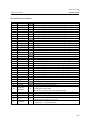
Sync Controller
YCbCr
Y
U
V
Progressive
YCbCr/RGB
SELECTOR
Interlace
YCbCr/RGB
Interlace
YCbCr/RGB
YCbCr
to
YUV
Y
LPF
C
Y/G
11bit DAC
Cb / B
11bit DAC
Cr / R
11bit DAC
YS
11bit DAC
CS
11bit DAC
CVBS
LPF
I2C Interface
SLA
SCL
SDA
TEST 5:0
FOUT
OCSYNC/OHSYNC
OVSYNC
OCLKX1
VSYNC_L
HSYNC_L
CSYNC_L
BLANK_L
Y / RGB
Level Adjustment
Interlace
to
Progressive
Progressive
YCbCr/RGB
RGB to YCbCr
YCbCr to RGB
Sync generator
Timing controller
Overlay & Color Bar
Controller
IMOD 2:0
IRGB
IPAL
IPRG
I444
ORGB
OPRG
CLKX2
RESET_L
Input Data
Decoder
Progressive
to
Interlace
11bit DAC
OKI Semiconductor
BLOCK DIAGRAM
OLC
OLR
OLG
OLB
YD 9:0
CD 9:0
BD 9:0
CGMS/WSS/CC
Contoller
Color Burst
Generator
Subcarrier
Generator
PEDL7655/56-000
ML86V7655/56
3/22
PEDL7655/56-000
OKI Semiconductor
ML86V7655/56
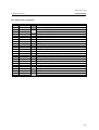
76 DVDD1
NC
78
77 FOUT
79 AGND
81 AVDD
80 Y/G
83 AGND
82 Cb/B
84 Cr/R
85 AVDD
86 AGND
87 XVREF
89 COMP
88 FS
91 CVBS
90 AVDD
92 AGND
93 CS
94 AVDD
95 NC
96 YS
97 AGND
98 NC
DGND1
100
99 NC
PIN CONFIGURATION (TOP VIEW)
NC 1
75 DGND1
DVDD1 2
74 STANDBY
SDA 3
73 OLC
SCL 4
72 OLR
SLA 5
71 OLG
MS 6
70 OLB
69 OCSYNC / OHSYNC
DGND2 7
DVDD2 8
68 OVSYNC
IMOD0 9
67 DGND2
IMOD1 10
66 DVDD2
IMOD2 11
65 BD0
IPAL 12
64 BD1
IRGB 13
63 BD2
IPRG 14
62 BD3
I444 15
61 BD4
ORGB 16
60 BD5
OPRG 17
59 BD6
RESET_L 18
58 BD7
TEST0 19
57 BD8
TEST1 20
56 BD9
TEST2 21
55 TEST5
TEST3 22
54 CD0
53 CD1
TEST4 23
52 CD2
CLKX2 24
51 DVDD2
CD3 49
DGND2 50
CD4 48
CD5 47
CD6 46
CD7 45
CD8 44
CD9 43
DGND1 42
YD0 41
YD1 40
YD2 39
YD4 37
YD3 38
YD6 35
YD5 36
DVDD1 34
YD7 33
YD8 32
YD9 31
BLNAK_L 30
VSYNC_L 28
HSYNC_L 29
OCLKX1 27
DVDD2 26
DGND2 25
100-Pin Plastic TQFP
4/22
PEDL7655/56-000
OKI Semiconductor
ML86V7655/56
PIN FUNCTION
Pin
1
2
3
4
5
Symbol
NC
DVDD1
SDA
SCL
SLA
Type
I/O
I
I
6
MS
I
7
8
9
10
11
DGND2
DVDD2
IMOD0
IMOD1
IMOD2
I
I
I
12
IPAL
I
13
IRGB
I
14
IPRG
I
15
I444
I
16
ORGB
I
17
OPRG
I
18
19
20
21
22
23
24
25
26
RESET_L
TEST0
TEST1
TEST2
TEST3
TEST4
CLKX2
DGND2
DVDD2
I
I
I
I
I
I
I
27
OCLKX1
O
28
VSYNC_L
I/O
29
HSYNC_L
I/O
30
BLANK_L
I/O
31
32
33
YD9
YD8
YD7
I
I
I
Description
No connection
I/O power supply (3.3 V)
Data pin for I2C bus (5 V tolerant pin)
Data pin for I2C bus (5 V tolerant pin)
I2C bus slave address least significant bit specification pin
Master/slave select pin
“1”: Master mode “0”: Slave mode
Core digital power supply (2.5 V)
Core digital power supply (2.5 V)
Input mode-0 control pin
Input mode-1 control pin
Input mode-2 control pin
PAL/NTSC mode select pin
“1”: PAL, “0”: NTSC
RGB/YCbCr input select pin
“1”: RGB input, “0”: YcbCr input
Progressive/interlaced input select pin
“1”: Progressive input, “0”: Interlaced input
4:2:2/4:4:4 select pin
“1”: 4:4:4 input, “0”: 4:2:2 input
RGB/YCbCr output select pin
“1”: RGB output, “0”: YcbCr output
Progressive output/interlaced output select pin
“1”: Progressive output, “0”: /Interlaced output
System reset pin. Reset at a “L” level.
Test mode control 0. Tie this pin to GND.
Test mode control 1. Tie this pin to GND.
Test mode control 2. Tie this pin to GND.
Test mode control 3. Tie this pin to GND.
Test mode control 4. Tie this pin to GND.
System clock input pin
Core digital GND
Core digital power supply (2.5 V)
CLKX1 output pin
Outputs 1/2-divided frequency of CLKX2
Vertical sync signal input-output pin
When in master mode: output; when in slave mode: input
Horizontal sync signal input-output pin
When in master mode: output; when in slave mode: input
BLANK signal input-output pin
When in master mode: output; when in slave mode: input
Video signal input pin; Brightness Y, G signal, bit[9]
Video signal input pin; Brightness Y, G signal, bit[8]
Video signal input pin; Brightness Y, G signal, bit[7]
5/22
PEDL7655/56-000
OKI Semiconductor
ML86V7655/56
PIN FUNCTION (continued)
Pin
34
35
36
37
38
39
40
41
42
43
44
45
46
47
48
49
50
51
52
53
54
55
56
57
58
59
60
61
62
63
64
65
66
67
68
Symbol
DVDD1
YD6
YD5
YD4
YD3
YD2
YD1
YD0
DGND1
CD9
CD8
CD7
CD6
CD5
CD4
CD3
DGND2
DVDD2
CD2
CD1
CD0
TEST5
BD9
BD8
BD7
BD6
BD5
BD4
BD3
BD2
BD1
BD0
DVDD2
DGND2
OVSYNC
Type
69
OCSYNC/
OHSYNC
O
70
71
72
OLB
OLG
OLR
I
I
I
73
OLC
I
74
STANDBY
I
I
I
I
I
I
I
I
I
I
I
I
I
I
I
I
I
I
I/O
I/O
I/O
I/O
I/O
I/O
I/O
I/O
I/O
I/O
I/O
O
Description
I/O power supply (3.3 V)
Video signal input pin; brightness Y, G signal, bit[6]
Video signal input pin; brightness Y, G signal, bit[5]
Video signal input pin; brightness Y, G signal, bit[4]
Video signal input pin; brightness Y, G signal, bit[3]
Video signal input pin; brightness Y, G signal, bit[2]
Video signal input pin; brightness Y, G signal, bit[1]
Video signal input pin; brightness Y, G signal, bit[0]
I/O GND
Video signal input pin; color difference C/Cr, R signal, bit[9]
Video signal input pin; color difference C/Cr, R signal, bit[8]
Video signal input pin; color difference C/Cr, R signal, bit[7]
Video signal input pin; color difference C/Cr, R signal, bit[6]
Video signal input pin; color difference C/Cr, R signal, bit[5]
Video signal input pin; color difference C/Cr, R signal, bit[4]
Video signal input pin; color difference C/Cr, R signal, bit[3]
Core digital GND
Core digital power supply (2.5 V)
Video signal input pin; color difference C/Cr, R signal, bit[2]
Video signal input pin; color difference C/Cr, R signal, bit[1]
Video signal input pin; color difference C/Cr, R signal, bit[0]
Test pin. Tie this pin to GND.
Video signal input pin; color difference Cb, B signal, bit[9]
Video signal input pin; color difference Cb, B signal, bit[8]
Video signal input pin; color difference Cb, B signal, bit[7]
Video signal input pin; color difference Cb, B signal, bit[6]
Video signal input pin; color difference Cb, B signal, bit[5]
Video signal input pin; color difference Cb, B signal, bit[4]
Video signal input pin; color difference Cb, B signal, bit[3]
Video signal input pin; color difference Cb, B signal, bit[2]
Video signal input pin; color difference Cb, B signal, bit[1]
Video signal input pin; color difference Cb, B signal, bit[0]
Core digital power supply (2.5 V)
Core digital GND
Component vertical sync signal output
Composite synchronization signal output/Component horizontal
synchronization signal output
Select either output with the internal register OCHSEL.
Overlay text color (blue) input pin
Overlay text color (green) input pin
Overlay text color (red) input pin
Transparency control. When set to “1”, an overlay signal is displayed.
Connect this pin to GND if it is not used.
Standby enable input pin
“1”: Standby, “0”: Normal operation
6/22
PEDL7655/56-000
OKI Semiconductor
ML86V7655/56
PIN FUNCTION (continued)
Pin
75
76
77
78
79
80
81
82
83
84
85
86
87
88
89
90
91
92
93
94
95
96
97
98
99
100
Symbol
DGND1
DVDD1
FOUT
NC
AGND
Y/G
AVDD
Cb/B
AGND
Cr/R
AVDD
AGND
XVREF
FS
COMP
AVDD
CVBS
AGND
CS
AVDD
NC
YS
AGND
NC
NC
DGND1
Type
O
O
O
O
I/O
I
O
O
O
O
Description
I/O GND
I/O power supply (3.3 V)
Field information signal output pin
No connection
Analog GND
Y/G output pin
Analog power supply
Cb/B output pin
Analog GND
Cr/B output pin
Analog power supply
Analog GND
Reference voltage input pin
Video output full-scale adjustment pin
Internal reference voltage output pin
Analog power supply
Composite signal output pin
Analog GND
Separate C signal output pin
Analog power supply
No connection
Separate Y signal output pin
Analog GND
No connection
No connection
I/O GND
7/22
PEDL7655/56-000
OKI Semiconductor
ML86V7655/56
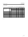
ABSOLUTE MAXIMUM RATINGS
Parameter
Symbol
Condition
Rating
Unit
Power supply voltage (I/O)
VDD1
Ta = 25°C
–0.3 V to +4.6 V
V
Power supply voltage (Core)
VDD2
Ta = 25°C
–0.3 V to +3.6 V
V
Power supply voltage (Analog)
AVDD
Ta = 25°C
–0.3 V to +4.6 V
V
Input voltage
VI
Ta = 25°C
–0.3 V to +6.0 V
V
Output short-circuit current
IOS
—
50
mA
Power dissipation
PD
Ta = 25°C
1
W
Storage temperature
Tstg
—
–55 to +150
°C
Caution: Product quality may suffer if any of the absolute maximum ratings above is exceeded, even for an
instant. That is, the absolute maximum ratings are rated values at which the product is on the verge of
suffering physical damage. Therefore the product must be used under conditions that ensure that no
absolute maximum rating will ever be exceeded.
RECOMMENDED OPERATING CONDITIONS
Parameter
Symbol
Min.
Typ.
Max.
Unit
Power supply voltage (I/O)
VDD1
3.0
3.3
3.6
V
Power supply voltage (Core)
VDD2
2.25
2.5
2.75
V
Power supply voltage (Analog)
AVDD
3.0
3.3
3.6
V
Ta
–40
—
+85
°C
External reference voltage
Vrefex
—
1.23
—
V
D/A output setting resistance
Riadj
500
1000
1330
Ω
RL
—
300
—
Ω
Operating temperature
D/A output load resistance
8/22
PEDL7655/56-000
OKI Semiconductor
ML86V7655/56
ELECTRICAL CHARACTERISTICS
DC Characteristics 1
Parameter
“H” level input voltage 1
Ta = –40 to +85°C, DVDD1 = 3.3 V ±0.3 V, VDD2 = 2.5 ±0.25 V, AVDD = 3.3 V ±0.3 V,
DGND1, DGND2, AGND = 0 V
Symbol
Condition
Min.
Typ.
Max.
Unit
VDD1
V
VIH1
—
2.2
—
+0.3V
*1
VIH2
—
2.2
—
5.5
V
VIL
–0.3
—
+0.8
V
“H” level input voltage 2
“L” level input voltage
Voltage at Schmitt trigger
threshold value
Voltage at Schmitt trigger
threshold value
Voltage at Schmitt trigger
hysteresis value
“H” level output voltage
“L” level output voltage
Input leakage current
“H” level input current (pull-down
resistance)
Output leakage current
Power supply current (during
operation)
Power supply current (when
stopped 1)
Power supply current (when
stopped 2)
VT+
—
—
—
2.1
V
VT-
—
0.7
—
—
V
VH
—
—
0.4
—
V
IOH = –4 mA
IOL = 4 mA
VIN = VDD1 or GND1
2.4
—
–10
—
—
—
—
0.4
+10
V
V
µA
IIH
VIN = VDD1
20
—
250
µA
ILO
VOUT = VDD1 or GND1
CLKX2 = 36 MHz,
RL = 300Ω
–10
—
+10
µA
—
—
160
mA
VOH
VOL
ILI
IDD1
IDDS1
CLKX2 = 0 MHz, VIN = VIL
—
—
45
mA
IDDS2
CLKX2 = 0 MHz, VIN = VIL
STANDBY = VIH
—
—
5
mA
*1: VIH2 is applied to the SDA and SCL pins only.
Note: The power supply current does not include the current consumption of the output buffer (no load).
DC Characteristics 2
Ta = –40 to +85°C, DVDD1 = 3.3 V ±0.3 V, VDD2 = 2.5 ±0.25 V, AVDD = 3.3 V ±0.3 V,
DGND1, DGND2, AGND = 0 V
Parameter
Symbol
Condition
Min.
Typ.
Max.
Unit
DAC internal reference voltage
VREFIN
—
1.187
1.23
1.313
V
DAC integral linearity
SINL
—
—
±4
—
LSB
DAC differential linearity
SDNL
—
—
±2
—
LSB
9/22
PEDL7655/56-000
OKI Semiconductor
ML86V7655/56
AC Characteristics
Parameter
Clock frequency
(CLKX2 frequency)
Clock duty ratio
Input data setup time
Input data hold time
Output delay time
Reset pulse time
I2C clock cycle time
I2C clock “H” level time
I2C clock “L” level time
I2C data setup time
I2C data hold time
Ta = –40 to +85°C, DVDD1 = 3.3 V ±0.3 V, VDD2 = 2.5 ±0.25 V, AVDD = 3.3 V ±0.3 V,
DGND1, DGND2, AGND = 0 V
Symbol
Condition
Min.
Typ.
Max.
Unit
NTSC square pixel
—
24.545454
—
MHz
PAL square pixel
—
29.5
—
MHz
NTSC 4Fsc
—
28.636364
—
MHz
FCLK
NTSC/PAL ITU-R BT601
—
27
—
MHz
NTSC/PAL ITU-R BT601
—
36
—
MHz
wide
dtCLK
—
45
—
55
%
tSI
—
6
—
—
ns
tHI
—
5
—
—
ns
tOD
CL = 20 pF
—
—
18
ns
tRSTP
—
100
—
—
ns
tCCI2C Rpull_up = 4.7 kΩ
10
—
—
µs
tHI2C Rpull_up = 4.7 kΩ
4
—
—
µs
tLI2C Rpull_up = 4.7 kΩ
4.7
—
—
µs
tDSI2C Rpull_up = 4.7 kΩ
250
—
—
ns
tDHI2C Rpull_up = 4.7 kΩ
0
—
3.45
µs
10/22
PEDL7655/56-000
OKI Semiconductor
ML86V7655/56
POWER-ON SEQUENCE
Turn on the power supplies in the following order: DVDD1 → AVDD → DVDD2. Turn them off in the reverse
order. After every power supply reaches its specified voltage and the clock CLKX2 is stabilized, input the reset
signal.
RESET INPUT TIMING
Input the reset signal for the reset pulse time tRSTP.
RESET_L
tRSTP
Figure 1 Reset Signal Input Timing
11/22
PEDL7655/56-000
OKI Semiconductor
ML86V7655/56
I2C INTERFACE TIMING
Use the I2C interface to set the internal register values. The I2C interface is compliant with the 100 kHz (SCL
frequency) standard mode. Figure 2 shows the basic timing. Make sure that the SDA value does not change while
SCL is at a “H” level. For information on timing parameter values refer to the AC characteristics.
MSB
SDA
SCL
1
S
2
7
8
9
1
2
9
P
ACK
Start Condition
tDSI2C
tDHI2C
tCCI2C
Stop Condition
tHI2C tLI2C
Figure 2 I2C Interface Basic Timing
Figures 3 and 4 show the I2C interface input format.
Write format
Slave
S
address
W
A
Subaddress
A
Data 0
A
………..
Data n
A
P
Figure 3 Write Format
Write data to the specified subaddress register. If multiple data items are written in succession, the subaddress is
incremented automatically for each data item.
Read format
Slave
S
address
W
A
Subaddress
A
Sr
Slave
address
R
A
Data
0
Am
………..
Data
n
Am
P
Figure 4 Read Format
Read data of the register at the specified subaddress. If multiple data items are written in succession, the
subaddress is incremented automatically for each data item.
Table 1 Symbols Used in the Input Formats
Symbol
Meaning
S
Start condition
Sr
Restart condition
Slave address
Slave address “100_010X”
Specify X from the SLA pin (“1” or “0”)
W
Write
R
Read
A
Acknowledge (slave)
Am
Acknowledge (master)
Sub address
Subaddress
Data n
Write and read data at subaddress
P
Stop condition
12/22
PEDL7655/56-000
OKI Semiconductor
ML86V7655/56
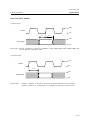
INPUT-OUTPUT TIMING
(1) Input timing
VIH
CLKX2
VIL
tSI
tHI
VIH
Input signal
VIL
Input signal: VSYNC_L, HSYNC_L, BLANK_L, IMOD0 to 3, IPAL, IRGB, IPRG, I444, ORGB, OPRG, MS,
YD, CD, BD OLC, OLR, OLG, OLB
(2) Output timing
VIH
CLKX2
VIL
TOD
VIH
Output signal
VIL
Output signal:
VSYNC_L, HSYNC_L, BLANK_L, OVSYNC, OCSYNC/OHSYNC, FOUT, OCLKX1
(VSYNC_L, HSYNC_L, and BLANK_L are configured as output pins in master mode.)
13/22
PEDL7655/56-000
OKI Semiconductor
ML86V7655/56
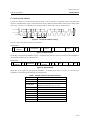
DESCRIPTION OF FUNCTIONAL BLOCKS
This section describes the functions of the blocks shown in the Block Diagram. For a detailed explanation of all
the functions, refer to the User’s Manual.
(1) Input Data Decoder
Converts the video data format based on the format of the digitally input video data. ITU BT.656, 20-bit
4:2:2 YCbCr, and 10-bit 4:2:2 YCbCr input data are converted to 4:4:4 YCbCr data. When ITU BT.656 is
input, the synchronization information is separated from the SAV and EAV information to generate a
synchronization signal. RGB input data is output to the next block.
The input video signal limiter function clips the input video signal at the quantization level (64–940)
specified by ITU-R BT601. In the extended luminance range mode, the limiter function clips the input video
signal at the quantization level (4–1016).
(2) Overlay & Color Bar Controller
A 3-bit title graphic and color bar are generated. The 3-bit title graphic becomes effective when the OLC pin
is set to “H”. The RGB graphic data input from the OLR, OLG and OLB pins can be replaced with input
video data in pixel units. The input video data supports YCbCr input, RGB input, interlaced input and
progressive input. With this function, letters can be displayed on the screen, as with the OSD function.
The built-in color bar becomes effective by setting the internal register value. The color bar is a color bar
with a luminance order (25%, 50%, 75% and 100%). It supports NTSC, PAL and YCbCr, RGB, CVBS,
S-Video, interlaced and progressive.
(3) Progressive to Interlace
Converts progressive video data (YCbCr, RGB) to interlaced video data. Progressive video data to be input
supports YCbCr (4:2:2 and 4:4:4) and RGB.
(4) Interlace to Progressive
Converts interlaced video data (YCbCr, RGB) to progressive video data.
(5) RGB to YCbCr/YCbCr to RGB
Converts RGB/YCbCr data to YCbCr/RGB data.
(6) Y/RGB Level Adjustment
This block adjusts the levels of the luminance signal Y, RGB data. The luminance signal level can be
adjusted in 16 steps (78.125% to 125%, in increments of 3.125%) by setting the internal register value. RGB
data gain can be set from 0.0 to 2.0 times by setting the internal register value. A different setting can be
made for each channel of R, G, and B.
(7) YCbCr to YUV
Converts YCbCr data to YUV data.
(8) Sync Controller
This block adds a synchronization signal to the video signal, adds VBI data, and adjusts the synchronization
signal level and offset of the signal.
(9) CGMS/WSS/CC Controller
This block generates data of CGMS-A(Copy Generation Management System - Analog), WSS (Wide Screen
Signaling), and CC (Closed Caption).
(10) LPF
Removes high frequency components from video data.
14/22
PEDL7655/56-000
OKI Semiconductor
ML86V7655/56
(11) Color Burst & Subcarrier Generator
These blocks generate the amplitude of the U and V components of a burst signal, and generate an color
subcarrier.
(12) 11-bit DAC
Converts digital video signals, with 11-bit resolution, to analog video signals and outputs them. The DAC
output is of the current drive type. Connect an external load resistor (300Ω) to the analog output pin.
Connect a video amplifier to the output stage of the encoder to drive a 75 Ω load.
(13) Sync Generator & Timing Controller
This block generates video synchronization signals and controls the timing of internal operations. A slave
mode and a master mode are available. In the slave mode, operation is based on synchronization signals input
from outside. In the master mode, operation is based on synchronization signals generated within the LSI.
(14) I2C Interface
I2C-bus serial interface. Used to set operation modes and internal register values.
15/22
PEDL7655/56-000
OKI Semiconductor
ML86V7655/56
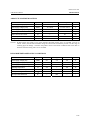
VIDEO DATA INPUT CONTROL
(1) Types of input video pixel frequencies
The ML86V7655/56 support the pixel frequencies for input video shown in Table 2. Every pixel frequency
can be selected.
(Note) The input clock frequency should be double the pixel frequency.
Table 2 Types of Input Pixel Frequencies
Input CLKX2
frequency (MHz)
Pixel frequency (MHz)
NTSC ITU-R BT601
13.5
27
PAL ITU-R BT601
13.5
27
NTSC Square Pixel
12.272727
24.545454
NTSC 4Fsc
14.318182
28.63634
PAL Square Pixel
14.75
29.5
NTSC ITU-R BT601 Wide
18.0
36
PAL ITU-R BT601 Wide
18.0
36
(2) Input data formats for interlaced and progressive scanning
Table 3 shows the scanning method (interlaced/progressive) and data type.
Table 3 Types of Input Data Formats
Scanning method
Interlaced
Interlaced
Interlaced
Progressive
Progressive
Progressive
Input data format
Sampling rate for color
Data type
difference
YCbCr
4:2:2 or 4:1:1 *1
YCbCr
4:4:4
RGB
4:4:4
YCbCr
4:2:2
YCbCr
4:4:4
RGB
4:4:4
Data input pin
YD/CD or YD *2
YD/CD/BD
YD/CD/BD
YD/CD
YD/CD/BD
YD/CD/BD
*1 : Change internal register value to select 4:2:2 or 4:1:1.
*2 : Use only the YD pin for video data/synchronized information multiplexing input (e.g., ITU-R BT-656).
Table 4 shows the available scanning methods for NTSC and PAL.
Table 4 Scanning Methods
Scanning method
NTSC interlaced
NTSC progressive
PAL interlaced
PAL progressive
No. of lines
Frequency
262.5
60 Hz
525
60 Hz
312.5
50 Hz
625
50 Hz
16/22
PEDL7655/56-000
OKI Semiconductor
ML86V7655/56
(3) Video data/synchronization information multiplexing input format types
The ML86V7655/56 support the video data/synchronization information multiplexing input interfaces and
data multiplexing (no multiplexing for sync signals) input interfaces shown in Table 5.
Table 5 Types of Multiplexed Input Interfaces
Input interface
NTSC ITU-R BT656 style(*1)
PAL ITU-R BT656 style(*1)
NTSC 4:2:2 10-bit multiplexing (no multiplexing for sync
signals)(*2)
NTSC Square Pixel 4:2:2 10-bit multiplexing (no multiplexing
for sync signals)(*2)
NTSC 4Fsc 4:2:2 10-bit multiplexing (no multiplexing for sync
signals)(*2)
PAL 4:2:2 10-bit multiplexing (no multiplexing for sync
signals)(*2)
PAL Square Pixel 4:2:2 10-bit multiplexing (no multiplexing
for sync signals)(*2)
NTSC Square Pixel ITU-R BT656 style(*3)
PAL Square Pixel ITU-R BT656 style(*3)
NTSC 4FSC ITU-R BT656 style(*3)
Input CLKX2
frequency (MHz)
27
27
Data input pin
YD
YD
27
YD
24.545454
YD
28.63634
YD
27
YD
29.5
YD
24.545454
28.63634
29.5
YD
YD
YD
*1: ITU-R BT656 style input interface. For details, refer to “Video Interface Timing” in the User’s Manual.
*2: 4:2:2 10-bit multiplexing (no multiplexing for sync signals) interface. This interface multiplexes
YCbCr and inputs the data from the YD pin. Input the synchronization signal from the VSYNC_L,
HSYNC_L and BLANK_L pins. For details, refer to the “Input Data Format” and “Video Interface
Timing” sections in the User’s Manual.
*3: ITU-R BT656 style input interface for SquarePixel and 4FSC. This interface multiplexes video data
and synchronization information and inputs the data from the YD pin. Synchronization information is
multiplexed as SAV and EAV. For details, refer to the “Video Interface Timing” section in the User’s
Manual.
17/22
PEDL7655/56-000
OKI Semiconductor
ML86V7655/56
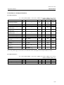
VIDEO DATA OUTPUT CONTROL
Video signals (composite signals, separate video signals and component YCbCr/RGB signals) can be
simultaneously output from the 6-channel D/A converter. Composite signals are output from the CVBS pin, and
separate video signals are output from the YA and CS pins. YCbCr or RGB signals are exclusively output from the
Y/G, Cb/B and Cr/R pins.
For each input data scanning method, conversion from interlaced to progressive and from progressive to interlaced
is possible. Color space conversion, such as YCbCr→RGB and RGB→YcbCr, is also possible. Table 6 shows the
available output formats for each input format.
For example, 4:2:2 YCbCr progressive video data can be simultaneously output in three different video formats,
composite, S-Video and YCbCr interlaced.
Table 6 Correspondence of Input Formats and Output Formats
Output format
Input format
4:2:2/4:1:1 YCbCr
4:4:4 YCbCr interlaced
4:2:2 YCbCr progressive
4:4:4 YCbCr progressive
RGB interlaced
RGB progressive
Composite
S-Video
{
{
{
{
{
{
{
{
{
{
{
{
YCbCr
YCbCr
RGB
RGB
interlaced
{
{
{
{
{
{
progressive
{
{
{
{
{
{
interlaced
{
{
{
{
{
{
progressive
{
{
{
{
{
{
{: Output enabled
Table 7 shows the output pins from which video data is output.
enable/disable D/A converter output for each channel.
Change the internal register values to
Table 7 Vidieo Output Pins
Output format
Pin name
Composite
CVBS
S-Video
YS, CS
YCbCr/RGB
interlaced/progressive
Y/G, Cb/B, Cr/R
18/22
PEDL7655/56-000
OKI Semiconductor
ML86V7655/56
INTERNAL REGISTERS
Use the I2C interface to change the internal register values. For details on register functions, refer to the User’s
Manual.
Table 8 Register Map
Sub address
Bit 7
Bit 6
00
01
02
03
04
05
06
07
08
09
0A
0B
0C
0D
EXTSEL
Reserved
SONSEL
CBON
MSSEL
IN2S
LDSEL
BBON
Reserved
0E
0F
10
11
12
13
14
15
16
17
18
19
1A
1B
to
Bit 5
Bit 4
Bit 3
Bit 2
Bit 1
Bit 0
Reserved
MLTDAT
IMODSEL[2:0]
I411
SPL411
NPSEL
I444SEL IRGBSEL IPRGSEL
PISEL
OFINV
OHCSEL
CSSEL ORGBSEL OPRGSEL
MCON
SBON
RGBLEV
SETUP
OUTLEV[1:0]
DMASK1
Reserved
DMASK2
Reserved
CNTCTL
TFON
Reserved
FRUN
BLKADJ[3:0]
Reserved
SYNCLEV1(CVBS)[2:0]
Reserved
SYNCLEV2(COMP)[2:0]
NOSIG
Reserved
LUMLEV[3:0]
GGAIN[7:0]
BGAIN[7:0]
RGAIN[7:0]
DACOFFSET[1:0]
DACOFF[5:0]
Reserved
Reserved
FFM
Reserved
Reserved
CCEN [1:0]
Reserved
CCLN [4:0]
CCOD0 [7:0]
CCOD1 [7:0]
CCED0 [7:0]
CCED1 [7:0]
Reserved
CCSTAT [1:0]
CGMSEN Reserved
WD01 [5:0]
WD02 [7:0]
CRCON Reserved
CRCDATA[5:0]
GP12 [7:0]
WSSEN Reserved
GP34 [5:0]
Reserved
3F
Reserved: Reserved for the system. Do not use these registers.
19/22
PEDL7655/56-000
OKI Semiconductor
ML86V7655/56
PACKAGE DIMENSIONS
(Unit: mm)
TQFP100-P-1414-0.50-K
Mirror finish
5
Package material
Lead frame material
Pin treatment
Package weight (g)
Rev. No./Last Revised
Epoxy resin
42 alloy
Solder plating (≥5µm)
0.55 TYP.
4/Oct. 28, 1996
Notes for Mounting the Surface Mount Type Package
The surface mount type packages are very susceptible to heat in reflow mounting and humidity absorbed in storage.
Therefore, before you perform reflow mounting, contact Oki’s responsible sales person for the product name,
package name, pin number, package code and desired mounting conditions (reflow method, temperature and
times).
20/22
PEDL7655/56-000
OKI Semiconductor
ML86V7655/56
REVISION HISTORY
Document
No.
PEDL7655-000
Date
Sep. 14, 2004
Page
Previous Current
Edition
Edition
–
–
Description
Preliminary edition 1
21/22
PEDL7655/56-000
OKI Semiconductor
ML86V7655/56
NOTICE
1. The information contained herein can change without notice owing to product and/or technical improvements.
Before using the product, please make sure that the information being referred to is up-to-date.
2. The outline of action and examples for application circuits described herein have been chosen as an explanation
for the standard action and performance of the product. When planning to use the product, please ensure that the
external conditions are reflected in the actual circuit, assembly, and program designs.
3. When designing your product, please use our product below the specified maximum ratings and within the
specified operating ranges including, but not limited to, operating voltage, power dissipation, and operating
temperature.
4. Oki assumes no responsibility or liability whatsoever for any failure or unusual or unexpected operation
resulting from misuse, neglect, improper installation, repair, alteration or accident, improper handling, or
unusual physical or electrical stress including, but not limited to, exposure to parameters beyond the specified
maximum ratings or operation outside the specified operating range.
5. Neither indemnity against nor license of a third party’s industrial and intellectual property right, etc. is granted
by us in connection with the use of the product and/or the information and drawings contained herein. No
responsibility is assumed by us for any infringement of a third party’s right which may result from the use
thereof.
6. The products listed in this document are intended for use in general electronics equipment for commercial
applications (e.g., office automation, communication equipment, measurement equipment, consumer
electronics, etc.). These products are not, unless specifically authorized by Oki, authorized for use in any
system or application that requires special or enhanced quality and reliability characteristics nor in any system
or application where the failure of such system or application may result in the loss or damage of property, or
death or injury to humans.
Such applications include, but are not limited to, traffic and automotive equipment, safety devices, aerospace
equipment, nuclear power control, medical equipment, and life-support systems.
7. Certain products in this document may need government approval before they can be exported to particular
countries. The purchaser assumes the responsibility of determining the legality of export of these products and
will take appropriate and necessary steps at their own expense for these.
8. No part of the contents contained herein may be reprinted or reproduced without our prior permission.
Copyright 2004 Oki Electric Industry Co., Ltd.
22/22