1
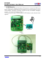
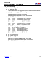
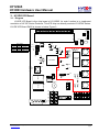
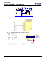
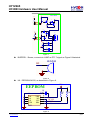
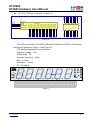
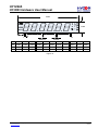
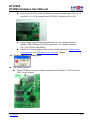
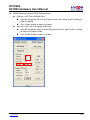
HY12S65 HY-IDE Hardware User Manual . © 2012 HYCON Technology Corp. www.hycontek.com APD-HYIDE011-V02_EN HY12S65 HY-IDE Hardware User Manual Table of Contents 1. HY-IDE STRUCTURE ............................................................................................................................... 4 2. HY-IDE USB CONTROL BOARD ............................................................................................................. 5 2.1. Diagram ................................................................................................................................................. 5 2.2. Circuit Description ................................................................................................................................. 6 3. HY-IDE ICE BOARD ................................................................................................................................. 7 3.1. Diagram ................................................................................................................................................. 7 3.2. Circuit Description ................................................................................................................................. 8 3.3. Circuit .................................................................................................................................................. 17 4. SIMPLE ERROR DETECTION ............................................................................................................... 18 4.1. ICE cannot connect to software .......................................................................................................... 18 4.2. Program Memory Loading Error ......................................................................................................... 21 5. . REVISION HISTORY .............................................................................................................................. 23 © 2012 HYCON Technology Corp www.hycontek.com APD-HYIDE011-V02_EN page2 HY12S65 HY-IDE Hardware User Manual Attention: 1. HYCON Technology Corp. reserves the right to change the content of this datasheet without further notice. For most up-to-date information, please constantly visit our website: http://www.hycontek.com . 2. HYCON Technology Corp. is not responsible for problems caused by figures or application circuits narrated herein whose related industrial properties belong to third parties. 3. Specifications of any HYCON Technology Corp. products detailed or contained herein stipulate the performance, characteristics, and functions of the specified products in the independent state. We does not guarantee of the performance, characteristics, and functions of the specified products as placed in the customer’s products or equipment. Constant and sufficient verification and evaluation is highly advised. 4. Please note the operating conditions of input voltage, output voltage and load current and ensure the IC internal power consumption does not exceed that of package tolerance. HYCON Technology Corp. assumes no responsibility for equipment failures that resulted from using products at values that exceed, even momentarily, rated values listed in products specifications of HYCON products specified herein. 5. Notwithstanding this product has built-in ESD protection circuit, please do not exert excessive static electricity to protection circuit. 6. . Products specified or contained herein cannot be employed in applications which require extremely high levels of reliability, such as device or equipment affecting the human body, health/medical equipments, security systems, or any apparatus installed in aircrafts and other vehicles. 7. Despite the fact that HYCON Technology Corp. endeavors to enhance product quality as well as reliability in every possible way, failure or malfunction of semiconductor products may happen. Hence, users are strongly recommended to comply with safety design including redundancy and fire-precaution equipments to prevent any accidents and fires that may follow. 8. Use of the information described herein for other purposes and/or reproduction or copying without the permission of HYCON Technology Corp. is strictly prohibited. © 2012 HYCON Technology Corp www.hycontek.com APD-HYIDE011-V02_EN page3 HY12S65 HY-IDE Hardware User Manual 1. HY-IDE Structure HY-IDE (HYCON - Integrated Development Environment) is composed by USB Control Board, ICE Board and Target Board that can emulate function and performance of HY12P series products. Through PC connection, HY-IDE can carry out emulation, debugging, program…etc. function as illustrated in Figure 1. The actual connection way of HY-IDE boards to HY-IDE software can be referred to below Figure1-1 PS 2 . Figure 1 Figure 1-1 © 2012 HYCON Technology Corp www.hycontek.com APD-HYIDE011-V02_EN page4 HY12S65 HY-IDE Hardware User Manual 2. HY-IDE USB Control Board 2.1. Diagram HY-IDE USB control board is the bridge that connects PC and HY-IDE ICE Board. Users can emulate HY11P Series products’ function and implement programming OTP products in the engineering stage by the control board, as shown in Figure 2. . Figure 2 © 2012 HYCON Technology Corp www.hycontek.com APD-HYIDE011-V02_EN page5 HY12S65 HY-IDE Hardware User Manual 2.2. Circuit Description Ports description of Figure 2: J4 : Adapter 9V input The internal is negative and the external is positive, providing programming power source (must be connected while OTP programming). U7 : USB connector to PC port Download program for emulation debug function Download programming program for HY12P Series products J1 : HY-ICE Board control port PIN 1 ICESDO connects to ICE_SDO of HY12S65 PIN 2 ICESDI connects to ICE_SDI of HY12S65 PIN 3 ICESCS connects to ICE_CS of HY12S65 PIN 4 VDD connects to ICE_VCC of HY12S65 PIN 5 ICESCK connects to ICE_SCK of HY12S65 PIN 6 VSS connects to ICE_VSS of HY12S65 J5 : HY12P series programming control port PIN 1 VPP (6V) connects to VPP of the IC PIN 2 ICECK connects to PSCK of the IC PIN 3 ICESDI connects to .PSDI of the IC PIN 4 ICESDO connects to PSDO of the IC PIN 5 VDD (3V) connects to VDD of the IC PIN 6 VSS connects to VSS of the IC S1 : IC Programming key S2 : IC Blank Check key D4 : Two color LED; Red LED: OTP programming, Blank Check…failure signal. Green LED: OTP programming, Blank Check…success signal. Green LED: USB/Adapter power-on signal. © 2012 HYCON Technology Corp www.hycontek.com APD-HYIDE011-V02_EN page6 HY12S65 HY-IDE Hardware User Manual 3. HY-IDE ICE Board 3.1. Diagram HY-IDE ICE Board is the chip board of HY12S65. Its main function is to implement emulation of HY12P Series Products. This ICE chip can directly emulate HY12P6X Series. HY-IDE ICE Board DK02 is shown in below Figure 3. 21 20 18 18 17 16 15 14 13 12 11 10 9 8 7 5 6 4 3 2 VBAT JP1 1 1 Batt S3 2 1 JP2 1 24C02 VDD_i C24 VDD_bat R36 VIN C9 C10 C12 R32 ON C11 R27 C4 C14 J11 C15 HY12S65 R39 P4 R28 C17 R29 R30 R31 C5 VDD_bat VIN 1 2 GS2612 C13 U9 Switch Remarks ON VIN~3V ON VDD_bat~3V ON VDD_i~3V S5 Power Select S5 VIN VDD_bat VDD_i VSSBAT U1 EXT 1 2 2 1 J1 3V 3 J2 Protection Circuit C6 Y1 C16 U4 3 1 2 4 ICESCK 5 R35 P1 ICEC ICESDO ICESDI VDD R33 . C7 R7 6 J3 VSS J14 R34 1 2 3 6 4 5 R26 3 2 1 U7 J5 J9 R22 1 2 3 R51 P2 J8 R23 U5 SRAM 1 2 3 S4 ON BUZZER1 U8 R25 R24 SRAM P3 BZ 8 6 4 2 9 7 5 3 1 SW3 RS1 6 7 8 9 SW7 1 2 3 4 5 JP4 2 1 J15 S2 SW2 SW6 10 11 ON SW1 ON SW4 SW5 S1 SW8 12 Figure 3 © 2012 HYCON Technology Corp www.hycontek.com APD-HYIDE011-V02_EN page7 HY12S65 HY-IDE Hardware User Manual 3.2. Circuit Description Below is the description of Figure 3 connector: J14: Connects to J1 PS2 communication port of HY-IDE USB Control Board. PC gives commands to HY12S65 through Control Board. It can download program to SRAM and can perform single execution, Free RUN…etc. debugging functions. S5: ICE board power selection (voltage from USB Control Board) VIN -When switched to ON, it represents VIN~3V voltage. VDD_bat - when switched to ON, it represents VDD_bat~3V voltage. VDD_i - when switched to ON, it represents VDD_i~3V voltage. Setup Ways of Power Selection: PC can supply power to ICE Board via USB or from external power sources. When it is powered by USB, the switches of S5 VIN and VDD_bat must turn to ON When it is powered by external power source, it must be connected though HY-IDE ICE Board Batt (JP1/JP2) and the switch of VDD_bat and VDD_i must be turned to OFF. J11: Can set up whether to short VIN and VDD_bat U7 & U8: SRAM J1 & J2: Program capacity selection of IC emulation chip . Byte), thus when HY12S65 is chosen, J8 HY12S65 ROM Size is16k Word (32K PIN 1-2 and J9 PIN 1-2 must be shorted When using HY12P series that has 8K Word (16K Byte) ROM Size or under, J8 PIN 2-3 and J9 PIN 2-3 must be shorted Y1, R39, C15 and C16 : connects to external crystal and peripheral capacitors and resistors C24: VDD power input regulated capacitor is recommended to keep in between 1uF to 10uF C13: VLCD power output regulated capacitor is recommended to keep in between 1uF ~ 4.7uF C4, C5, C10, C11, C12, C13 and C14: Analog power regulated capacitor In order to enhance the operation performance of ADC, the regulated capacitor is suggested to locate as closer to the pin as possible. C4:REFO-AGND capacitor: 100nF C5:AGND capacitor: 100nF C10:VGG capacitor: 1uF C11:VDDA capacitor: 1uF C12:CA & CB capacitor: 100nF C13:VLCD capacitor: 1uF C14:ACM capacitor: 100nF © 2012 HYCON Technology Corp www.hycontek.com APD-HYIDE011-V02_EN page8 HY12S65 HY-IDE Hardware User Manual Power system: ICE power system can be supply by 3V regulated power of HY-IDE USB Control Board or by external input power (the external power input cannot exceed 3.6V as the datasheet specified). When ICE emulates, it only need to connect U7 USB of HY-IDE USB Control Board to PC end to supply ICE power. USB power and external power will be introduced in below: USB power: When using USB power supply, VDD_bat and VDD_i switch of HY-IDE ICE Board S5 must be turned to ON so that ICE can be powered by 3V USB regulated voltage. To measure IC consumption current, the switch must configure VIN and VDD_bat to ON and power by USB regulated 3V and measure the current consumption from J1 of HY-IDE ICE Board. External Power: Users must be careful when using external power, the VIN, VDD_bat and VDD_i option of S5 switch of HY-IDE ICE Board must be switched to OFF status first. External power can be input from JP1 VBAT positive end, VSSBAT negative end of HY-IDE ICE Board and S3 is. the power on/off control. J2: power select (whether the system power passes through Regulator (U1)) J2 PIN 1-2 short means, inputting VBAT external power input to U1, supplying the whole system regulated 3V power from VDD_i (to change output voltage, R40, R41 & R42, its equation is: VOUT 1.240V (1 R 40 R 41 ) ). R 42 J2 PIN 2-3 short means, VBAT power directly input to VDD_i (the external power input cannot exceed 3.6V as the datasheet specified). J1: Can connect to current meter, testing the whole VDD_i current consumption. It must be shorted if current meter was not connected, VDD_bat voltage will equals to that of VDD_i, as shown in Figure 4. Users must pay attention that VDD_bat voltage will equal to VDD_i voltage when J1 short. If using external power, then VIN, VDD_bat and VDD_i options of S5 switch must be switched to OFF status to continue the following operations as to prevent hardware damage resulted from power backflow of HY-IDE USB Control Board, showing in Figure 4. © 2012 HYCON Technology Corp www.hycontek.com APD-HYIDE011-V02_EN page9 HY12S65 HY-IDE Hardware User Manual *. POWER NET 1 2 J1 Current test VDD_bat VDD J2 EXT 3 2 3V 1 C3 10uF C1 0.1uF 5 VIN 3 1N4001 4 VDD Sel R40 100K C2 10uF R41 42.2K R42 100K JP1 VBAT S3 D1 1 2 3 4 EN IN OUT ADJ U1 GND GND GND GND ON1 COM1 1 OFF1 6 ON2 COM2 2 OFF2 Batt JP2 VSSBAT 8 7 6 5 GS2612 Figure 4 RST Circuit:Please refer to Figure 5 in below. . Figure 5 JP4: SPI communication port, as shown in Figure 6. PIN1 VDD JP4 PIN2 PT1.2 (SDI) 1 3 PIN3 PT1.6 (SCK) 5 PIN4 PT1.5 (SDO) 7 9 PIN5 PT1.1 (CS) 11 PIN6 VSS 2 4 6 8 10 12 KEY3 KEY5 KEY4 KEY2 SDI(PT1.2) SCK(PT1.6) SDO(PT1.5) SCS(PT1.1) SPI Figure 6 RS1:UART communication port (RS232). Commonly use 9-PIN female header, as shown in Figure 7. © 2012 HYCON Technology Corp www.hycontek.com APD-HYIDE011-V02_EN page10 HY12S65 HY-IDE Hardware User Manual Photo RS232 IV+ VDD R43 10k R9 500R D4 TX 1 2 R46 270R R44 500R U2 P N 1N4148 4 3 C E Q1 IGND PC817 Q2 R45 6.8k IV- D2 1N4148 VDD R11 500R D3 1N4148 RS1 R10 500R PC_RXD IVD5 1N4148 U3 RX 4 3 C E P N 1 2 PC_TXD PC817 1 6 2 7 3 8 4 9 5 IGND IV+ D6 1N4148 C18 10uF D7 1N4148 C19 10uF IGND D8 1N4148 D9 1N4148 IV- Figure 7 BUZZER1:Buzzer, connects to JUMP as PT1.7 signal as Figure 8 illustrated. . BUZZER1 BZ Figure 8 U9:EEPROM 24C02, as described in Figure 9. VDD EEPROM C8 0.1uF R37 10k U9 1 2 3 4 A0 A1 A2 VSS VDD WP SCL SDA 8 7 6 5 R38 IIC_SCL IIC_SDA 24C02 Figure 9 © 2012 HYCON Technology Corp www.hycontek.com APD-HYIDE011-V02_EN page11 HY12S65 HY-IDE Hardware User Manual COM 0 COM 2 SEG0 SEG2 SEG4 SEG6 SEG8 SEG10 SEG12 SEG14 J10, JP3:LCD pin, as shown in Figure 10. J10 LCD_20*4 LCD_20*4 JP3 LCD 1 3 5 7 9 11 13 15 17 19 COM0 COM1 COM2/SEG0 COM3/SEG1 SEG2 SEG3 SEG4 SEG5 SEG6 SEG7 SEG8 SEG9 SEG10 SEG11 SEG12 SEG13 SEG14 SEG15 SEG16 SEG17 SEG18 SEG19 SEG20 SEG21 1 2 3 4 COM 1 COM 3 SEG1 SEG3 SEG5 SEG7 SEG9 SEG11 SEG13 SEG0 SEG1 SEG2 SEG3 SEG4 SEG5 SEG6 SEG7 SEG8 SEG9 SEG10 SEG11 SEG12 SEG13 SEG14 5 6 7 8 9 10 11 12 13 14 15 16 17 18 19 20 21 22 23 24 COM0 COM1 COM2 COM3 2 4 6 8 10 12 14 16 18 20 Figure 10 The LCD specification of HY-IDE ICE Board is molded by HYCON, LCD symbols and pins are depicted in Figure 11 and Figure 12. LCD detailed specifications are as follows: Operation voltage:3.0V Visible angle:60。 Operation frequency:60Hz . Bias:1/3 bias Waveform:1/4 duty Pin:90 degree COM1 COM2 COM3 COM4 SEG1 SEG2 SEG3 SEG4 SEG5 SEG6 SEG7 SEG8 SEG9 SEG10 SEG11 SEG12 SEG13 SEG14 SEG15 SEG16 SEG17 S18 1A 1E 2A 2E 3A 3E 4A 4E 5A 5E 6A 6E S1 S5 S10 S9 1B 1F 2B 2F 3B 3F 4B 4F 5B 5F 6B 6F S2 S6 S14 S19 S11 1C 1G 2C 2G 3C 3G 4C 4G 5C 5G 6C 6G S3 S7 S15 S20 S12 1D 1H 2D 2H 3D 3H 4D 4H 5D 5H 6D S17 S4 S8 S16 S21 S13 Figure 11 © 2012 HYCON Technology Corp www.hycontek.com APD-HYIDE011-V02_EN page12 HY12S65 HY-IDE Hardware User Manual 70mm m A K M V g TARE ZERO 27mm 17.78mm 8.89mm 1 21 0.812mm 2.54mm PIN 1 2 3 4 5 6 7 8 9 10 11 I/O COM1 COM2 COM3 COM4 SEG1 SEG2 SEG3 SEG4 SEG5 SEG6 SEG7 PIN 12 13 14 15 16 17 18 19 20 21 I/O SEG8 SEG9 SEG10 SEG11 SEG12 SEG13 SEG14 SEG15 SEG16 SEG17 Figure 12 . © 2012 HYCON Technology Corp www.hycontek.com APD-HYIDE011-V02_EN page13 HY12S65 HY-IDE Hardware User Manual Y1, C15 and C16: connects to external Crystal oscillation circuit, as shown in Figure 13. HY-IDE ICE Board already connects to Y1-4MHZ oscillator for user application. C15 XOUT 15pF R39 1M Y1 4Mhz C16 XIN 15pF Figure 13 SW1, SW2, SW3, SW4, SW5, SW6, SW7 & SW8:Can use KEY1~KEY6 to carry out 8 sets key scan, as shown in Figure 14. PT1.0(IN) PT1.1(IN) Function1 SW1 Hz%1 SW2 SW SW3 REL1 SW4 RANGE1 SW5 HOLD1 SW6 MAX/MIN1 SW7 BACKLIGHT1 SW8 KEY1 KEY2 . PT1.2(IN) KEY3 PT1.5(IN/OUT) KEY4 PT1.6(IN/OUT) KEY5 KEY6 PT3.7(IN/OUT) or PT2.7(IN/OUT) Figure 14 S4:Function switch pin for PT2.4~PT2.7, as shown in Figure 15. Figure 15 © 2012 HYCON Technology Corp www.hycontek.com APD-HYIDE011-V02_EN page14 HY12S65 HY-IDE Hardware User Manual S1 and S2:Divided by resistors (R1~R4、R12~R15), using comparator to form 16 sets key scan. CMP2 PT2.6 R1 20K R2 20K R3 20K R4 20K S2 16 15 14 13 CMP1 12 PT2.5 11 10 9 S1 1 2 3 4 5 6 7 8 R12 20K CMP1 1 2 3 4 5 6 7 8 16 CMP0 15 PT2.4 14 13 12 11 10 9 CMP0 R13 20K R14 20K R15 20K . Figure 16 © 2012 HYCON Technology Corp www.hycontek.com APD-HYIDE011-V02_EN page15 HY12S65 HY-IDE Hardware User Manual 3 Digital Multi-meter (DMM) application measurement circuit: shown in Figure 17 (the diagram is circled in red as in Figure 3). 10K 9013 J5 PBx P4 Vol/Ohm/Cap/DT B E R22 99 J4 JUMP R32 10M0.7% RLU R29 R30 MOV2 TVR MOV3 TVR TVR B R51 C B 該COM點代表直接拉回AGND Q4 9013 E 2 PB0 PB1 PB1 PB3 PB4 PB5 CMP0 CMP1 CMP2 CMP3 KEY1 KEY2 PA0 PA1 PA2 PA3 PA4 PA5 PA6 RLD RLU 1uF PB0 R35 1M 75 74 73 72 71 70 69 68 67 66 65 64 63 62 61 60 59 58 57 56 55 54 53 52 51 C4 0.1uF Q3 9013 CNT 1u 3 C6 C5 PB1 J7 HZ COM R33 100 AGND R34 JUMP 100K 2 27nF COM C7 RLD MOV1 JUMP J6 Vol/Ohm/Cap/DT R7 1M 900K 10M 104 10K 0.1% 1K 0.1% COM 該COM點代表直接拉回AGND PTC1 PTC R31 1.11M 0.1% 101K 0.1% C17 R24 0.01 Vol/Ohm/Cap/DT 3 R27 R28 J16 JUMP PTC E P3 A R23 0.99 1M PTC2 VDD 3 Current mA 2 9013 C 1 2 3 C Q6 J3 11 P2 mA/uA PB1 11 6 5 4 3 2 1 R26 10K uA 2 B C PB3 E R25 PB5 PB4 PB3 PB1 PB1 PB0 Q5 該COM點代表直接拉回AGND P1 COM COM U4 AGND REFO PA0 PA1 PA2 PA3 PA4 PA5 PA6 RLD RLU FTN FTP PB0 PB1 PB2 PB3 PB4 PT3.5/PB5 PT2.4/CM P0 PT2.5/CM P1 PT2.6/CM P2 PT2.7/CM P3 PT1.0/INT0/PSCK PT1.1/INT1/PSDI/SCE AVSS . COM0 COM1 COM2 COM3 SEG0 SEG1 SEG2 SEG3 SEG4 SEG5 SEG6 SEG7 SEG8 SEG9 ACM VDDA VGG CA CB VSS VPP/RST VDD VLCD COM0 COM1 COM2 COM3 NC NC SEG0 SEG1 SEG2 SEG3 SEG4 SEG5 SEG6 SEG7 SEG8 SEG9 HY12S65_LQFP100 SEG10 SEG11 SEG12 SEG13 SEG14 PT3.7/CM PO PT3.6/CNT PT2.3/TM CKI PT2.2/PWM/PFD PT2.1/XTI PT2.0/XTO VDD_ICE VSS ICE_SDI ICE_SDO ICD_SCK ICE_CS ICE_CS0 ICD_RD ICE_WE ICE_DA0 ICE_DA1 ICE_DA2 ICE_DA3 ICE_DA4 GND RST VDD 76 77 78 79 80 81 82 83 84 85 86 87 88 89 90 91 92 93 94 95 96 97 98 99 100 PT1.2/SDI PT1.3/RX/TST PT1.4/TX PT1.5/SDO PT1.6/SCK PT1.7/BZ/PSDO ICE_ADR15 ICE_ADR14 ICE_ADR13 ICE_ADR12 ICE_ADR11 ICE_ADR10 ICE_ADR9 ICE_ADR8 ICE_ADR7 ICE_ADR6 ICE_ADR5 ICE_ADR4 ICE_ADR3 ICE_ADR2 ICE_ADR1 ICE_ADR0 ICE_DA7 ICE_DA6 ICE_DA5 50 KEY3 49 RX 48 TX 47 KEY4 46 KEY5 45 BZ 44 _SBM-SEL 43 _ADR14 _ADR13 42 41 _ADR12 40 _ADR11 _ADR10 39 _ADR9 38 37 _ADR8 36 _ADR7 _ADR6 35 _ADR5 34 _ADR4 33 _ADR3 32 _ADR2 31 30 _ADR1 29 _ADR0 _DA7 28 _DA6 27 26 _DA5 1 SEG10 2 SEG11 3 SEG12 SEG13 4 SEG14 5 6 CMPO CNT 7 IIC_SDA 8 IIC_SCL 9 10 XIN XOUT 11 12 13 14 _SDI _SDO 15 16 _SCK _SCS 17 _CS 18 _RD 19 _WE 20 _DA0 21 _DA1 22 _DA2 23 _DA3 24 _DA4 25 HY12S65 Figure 17 © 2012 HYCON Technology Corp www.hycontek.com APD-HYIDE011-V02_EN page16 HY12S65 HY-IDE Hardware User Manual 3.3. Circuit Please refer to Figure 18 in below. 16 15 14 13 CMP1 12 PT2.5 11 10 9 PT1.0(IN) 1 2 3 4 5 6 7 8 1 CMP2 PT2.6 1 2 3 4 5 6 7 8 S1 CMP0 2 16 CMP0 15 PT2.4 14 13 12 11 10 9 S4 1 2 3 4 J10 LCD_20*4 J3 1 2 3 3 Current VDD AGND J2 RLU PB1 C5 C2 10uF C1 0.1uF C17 J5 PBx C3 10uF R40 100K R41 42.2K R42 100K J4 JUMP R29 R30 R31 10M HY12S65_LQFP100 C23 D1 1N4001 1 2 3 4 4 EN IN OUT ADJ U1 TVR Batt JP1 VBAT JP2 VSSBAT U4 R34 PB0 PS2-6PIN J14 B B 50 KEY3 49 RX 48 TX 47 KEY4 46 KEY5 45 BZ _SBM-SEL 44 _ADR14 43 _ADR13 42 _ADR12 41 _ADR11 40 39 _ADR10 38 _ADR9 _ADR8 37 _ADR7 36 _ADR6 35 _ADR5 34 _ADR4 33 _ADR3 32 _ADR2 31 _ADR1 30 29 _ADR0 _DA7 28 _DA6 27 _DA5 26 Vol/Ohm/Cap/DT Q4 9013 Q3 9013 MOV3 MOV2 TVR 8 7 6 5 B B J16 JUMP 6 ON2 COM2 2 OFF2 S3 5 VIN ON1 COM1 1 OFF1 *. POWER NET 3 4 GND GND GND GND 2 TVR MOV1 GS2612 PTC2 PTC PTC1 PTC JUMP 2 PT1.2/SDI PT1.3/RX/TST PT1.4/TX PT1.5/SDO PT1.6/SCK PT1.7/BZ/PSDO ICE_ADR15 ICE_ADR14 ICE_ADR13 ICE_ADR12 ICE_ADR11 ICE_ADR10 ICE_ADR9 ICE_ADR8 ICE_ADR7 ICE_ADR6 ICE_ADR5 ICE_ADR4 ICE_ADR3 ICE_ADR2 ICE_ADR1 ICE_ADR0 ICE_DA7 ICE_DA6 ICE_DA5 1 2 3 4 5 6 HY12S65 VDD_bat R55 R54 47K 47K _SDO _SDI _SCS _SCK J15 Power JP4 1 3 5 7 9 11 2 SPI Q5 9013 Q6 2 9013 VDD 2 4 6 8 10 12 RLD PB1 R51 1 2 4 5 _VSS_ram S VDD 5 U2 P N PC817 R10 500R 4 3 14 13 12 10 9 PC817 R35 1M VIN VDD_bat 5 C E P N IV+ R43 10k 4 3 D2 8 11 7 R44 500R Q1 Date: File: C Size Title 6.8k R45 IV- D6 1N4148 D7 1N4148 D8 1N4148 D9 1N4148 1 2 3 4 5 6 7 8 9 10 11 12 13 14 1 2 3 4 5 6 7 8 9 10 11 12 13 14 VCC WE A13 A8 A9 A11 OE A10 CE I/O7 I/O6 I/O5 I/O4 I/O3 VCC WE A13 A8 A9 A11 OE A10 CE I/O7 I/O6 I/O5 I/O4 I/O3 Q2 6 6 Sheet of Drawn By: VDD_bat _WE _ADR13 _ADR8 _ADR9 _ADR11 _RD _ADR10 _CSRAM_S _DA7 _DA6 _DA5 _DA4 _DA3 VDD_bat _WE _VSS_ram _ADR8 _ADR9 _VSS_ram _RD _ADR10 _CSSBM _DA7 _DA6 _DA5 _DA4 _DA3 SBMMemory 28 27 26 25 24 23 22 21 20 19 18 17 16 15 Program Memory 28 27 26 25 24 23 22 21 20 19 18 17 16 15 _CS *. ICE Memory NET RS1 R46 270R Photo RS232 D4 1 6 2 7 3 8 4 9 5 J9 CSSel 1N4148 PC_RXD PC_TXD _CSRAM U7 A14 A12 A7 A6 A5 A4 A3 A2 A1 A0 I/O0 I/O1 I/O2 GND 62256 U8 A14 A12 A7 A6 A5 A4 A3 A2 A1 A0 I/O0 I/O1 I/O2 GND 62256 19-Jun-2012 Y:\MyDesign.ddb A10004 Number HY12S65 ICE _VSS_ram _VSS_ram _ADR7 _ADR6 _ADR5 _ADR4 _ADR3 _ADR2 _ADR1 _ADR0 _DA0 _DA1 _DA2 _VSS_ram _ADR12 _ADR7 _ADR6 _ADR5 _ADR4 _ADR3 _ADR2 _ADR1 _ADR0 _DA0 _DA1 _DA2 _VSS_ram _SBM-SEL IVD5 1N4148 D3 1N4148 1N4148 IV+ R11 500R IGND U3 1 2 IGND C18 10uF J8 SBMSel IV- C19 10uF IGND _ADR14 U5C 7400 U5D 7400 C20 VDD_bat _VSS_ram _VCC_ram 0.1uF 6 5 4 _VSS_ram Power Sel S5 VDD_bat CNT R7 1M VDD 3 6 C E SDI(PT1.2) SCK(PT1.6) SDO(PT1.5) SCS(PT1.1) 1 2 R9 500R VDD TX 1u C7 RX KEY3 KEY5 KEY4 KEY2 JUMP J7 HZ U5A 7400 U5B 7400 VIN VDD_bat VDD 2 1 J11 VDD_Bat VIN 1 VDD_bat2 VDD_i 3 該COM點代表直接拉回AGND COM 1uF VDD_bat _VCC_ram _VSS_ram R53 47K _VSS_ram _VCC_ram 100K 27nF R33 100 J6 Vol/Ohm/Cap/DT R32 10M0.7% P4 Vol/Ohm/Cap/DT C6 1.11M 0.1% 1uF 101K 0.1% AVSS PB3 EXT 3 2 3V 1 C4 0.1uF R27 R28 VDD Sel R26 10K 10K R25 VDD_bat J1 Current test COM GND RST VDD COM0 COM1 COM2 COM3 76 77 78 79 80 81 82 83 84 85 86 87 88 89 90 91 92 93 94 95 96 97 98 99 100 ACM VDDA VGG CA CB VSS VPP/RST VDD VLCD COM0 COM1 COM2 COM3 NC NC SEG0 SEG1 SEG2 SEG3 SEG4 SEG5 SEG6 SEG7 SEG8 SEG9 J12 CNT _VSS_ram J13 ICE Signal R49 900K AVSS COM 該COM點代表直接拉回AGND R24 0.01 R23 0.99 1M R22 99 該COM點代表直接拉回AGND P1 COM COM uA mA P2 mA/uA P3 A R48 C13 1u AVSSC14 0.1UF AVSSC11 C10 1UF 1UF C12 0.1UF C24 1u SEG0 SEG1 SEG2 SEG3 SEG4 SEG5 SEG6 SEG7 SEG8 SEG9 10K 0.1% LCD_20*4 C9 10n R36 100k VDD V04 change PT2.7(IN/OUT) CMP3 R5 OPEN KEY6 R6 0 CMPO PT3.7(IN/OUT) COM0 COM1 COM2/SEG0 COM3/SEG1 104 REL1 SW4 功能切換 SW SW3 COM0 COM1 COM2 COM3 XIN Y1 4Mhz XOUT BUZZER1 R39 1M 1 2 R1 20K R2 20K R3 20K R4 20K R12 20K R13 20K R14 20K Hz%1 SW2 R15 20K Function1 SW1 BACKLIGHT1 SW8 R38 MAX/MIN1 SW7 R37 10k VDD HOLD1 SW6 IIC_SCL IIC_SDA RANGE1 SW5 C8 0.1uF 8 7 6 5 BZ C15 15pF C16 15pF 4 3 E C 11 C E 3 S2 CMP1 KEY1 KEY2 U9 VDD WP SCL SDA EEPROM A0 A1 A2 VSS 24C02 JP3 LCD 3 1K 0.1% PT1.1(IN) KEY3 PT1.2(IN) PT1.5(IN/OUT) KEY4 PT1.6(IN/OUT) KEY5 KEY6 PT3.7(IN/OUT) or PT2.7(IN/OUT) 1 2 3 4 2 1 2 3 1 D C B A 1 1 2 3 1 3 E C 11 C21 VDD_bat _VSS_ram 0.1uF C22 VDD_bat 0.1uF _VSS_ram Revision V04 D C B A APD-HYIDE011-V02_EN page17 © 2012 HYCON Technology Corp www.hycontek.com 2 1 PB0 PB1 PB1 PB3 PB4 PB5 CMP0 CMP1 CMP2 CMP3 KEY1 KEY2 C E 3 PB5 PB4 PB3 PB1 PB1 PB0 1 2 3 4 5 6 . 6 5 4 3 2 1 PA0 PA1 PA2 PA3 PA4 PA5 PA6 RLD RLU 75 74 73 72 71 70 69 68 67 66 65 64 63 62 61 60 59 58 57 56 55 54 53 52 51 AGND REFO PA0 PA1 PA2 PA3 PA4 PA5 PA6 RLD RLU FTN FTP PB0 PB1 PB2 PB3 PB4 PT3.5/PB5 PT2.4/CMP0 PT2.5/CMP1 PT2.6/CMP2 PT2.7/CMP3 PT1.0/INT0/PSCK PT1.1/INT1/PSDI/SCE SEG10 SEG11 SEG12 SEG13 SEG14 PT3.7/CM PO PT3.6/CNT PT2.3/TM CKI PT2.2/PWM/PFD PT2.1/XTI PT2.0/XTO VDD_ICE VSS ICE_SDI ICE_SDO ICD_SCK ICE_CS ICE_CS0 ICD_RD ICE_WE ICE_DA0 ICE_DA1 ICE_DA2 ICE_DA3 ICE_DA4 SEG10 1 2 SEG11 3 SEG12 SEG13 4 SEG14 5 CMPO 6 CNT 7 IIC_SDA 8 IIC_SCL 9 XIN 10 XOUT 11 12 _VSS_ram 13 _SDI 14 _SDO 15 16 _SCK 17 _SCS _CS 18 _RD 19 _WE 20 _DA0 21 _DA1 22 _DA2 23 _DA3 24 _DA4 25 CNT CMPO 2 1 1 2 SEG2 SEG3 SEG4 SEG5 SEG6 SEG7 SEG8 SEG9 SEG10 SEG11 SEG12 SEG13 SEG14 SEG15 SEG16 SEG17 SEG18 SEG19 SEG20 SEG21 5 6 7 8 9 10 11 12 13 14 15 16 17 18 19 20 21 22 23 24 SEG0 SEG1 SEG2 SEG3 SEG4 SEG5 SEG6 SEG7 SEG8 SEG9 SEG10 SEG11 SEG12 SEG13 SEG14 CMP3 PT2.7 CMP2 PT2.6 CMP1 PT2.5 CMP0 PT2.4 4 3 2 1 5 6 7 8 COM0 COM2 SEG0 SEG2 SEG4 SEG6 SEG8 SEG10 SEG12 SEG14 2 4 6 8 10 12 14 16 18 20 1 3 5 7 9 11 13 15 17 19 COM 1 COM 3 SEG1 SEG3 SEG5 SEG7 SEG9 SEG11 SEG13 Figure 18 HY12S65 HY-IDE Hardware User Manual 4. Simple Error Detection 4.1. ICE cannot connect to software Simple error correction is described as follows when ICE cannot connect to software: Hardware configuration, IDE mode error detection: Options =>Interface Setup =>Interface Mode defaults as USB IDE Mode is emulation and Debug . © 2012 HYCON Technology Corp www.hycontek.com APD-HYIDE011-V02_EN page18 HY12S65 HY-IDE Hardware User Manual Power System Debug: This action is to testify whether HY-IDE USB Control Board is completely connected to PC through USB port and the regulated 3V voltage output functions normally. Options =>ICE Test => Click CK ALL and confirm VCC voltage is close to 3V. When Control Board only connects to USB port, the voltage of VPP closes to 5V; when Adapter 9V of J4 is connected, VPP voltage will close to 6.3V. . © 2012 HYCON Technology Corp www.hycontek.com APD-HYIDE011-V02_EN page19 HY12S65 HY-IDE Hardware User Manual ICE Power Debug: When using USB to supply power, a few switches must be inspected to ensure ICE chip operates normally. ICE Board S5, switching VIN, VDD_bat to ON Short ICE Board J2 PIN1-2, J1 and S3 switch turns to ON . Using voltage meter to check whether there is a 3V voltage existed in between VDD (PIN83)-VSS (PIN81) and also a 3V voltage in between ICE_VCC (PIN12)-VSS (PIN81). If there is no such voltage existed, please double check the ”Power system error detection” and ”ICE power error detection” chapter. Using external power supply, please check the following switched: Switching VIN, VDD_bat and VDD_i to “OFF” of the ICE Board S5. © 2012 HYCON Technology Corp www.hycontek.com APD-HYIDE011-V02_EN page20 HY12S65 HY-IDE Hardware User Manual Connecting JP1/JP2 of the ICE Board to external voltage input, short J1, J2 and PIN1-2 (if >3V is needed, short J2 PIN2-3). Switching S3 to “ON”. Using voltage meter to check whether there is a 3V voltage existed in between VDD (PIN83)-VSS (PIN81) and also a 3V voltage in between ICE_VCC (PIN12)-VSS(PIN81). If there is no such voltage existed, please double check the ”Power system error detection” and ”ICE power error detection” chapter. 4.2. Program Memory Loading Error . ICE SRAM detection: Check ICE Board J8 and J9. When emulating HY12S65(8K), J1 PIN1-2 and J2 PIN1-2 must be short. © 2012 HYCON Technology Corp www.hycontek.com APD-HYIDE011-V02_EN page21 HY12S65 HY-IDE Hardware User Manual SRAM Data and Program ROM Data detection: Options =>ICE Test =>SRAM Data Input 80 in Address, AA in Write Data and then click “Write” button. Writing all data into SRAM. Click “Read” button to read out all data. Options =>ICE Test =>Program ROM Data Input 80 in Address, 5AA5 in Write Data and then click “Write” button. Writing all data into Program ROM. Click “Read” button to read out all data. . © 2012 HYCON Technology Corp www.hycontek.com APD-HYIDE011-V02_EN page22 HY12S65 HY-IDE Hardware User Manual 5. Revision History Major differences are stated thereinafter: Version Page V02 ALL Revision Summary First edition . © 2012 HYCON Technology Corp www.hycontek.com APD-HYIDE011-V02_EN page23