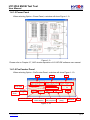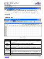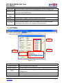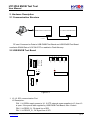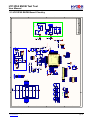
1
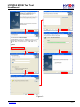
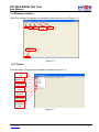
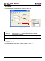
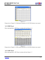
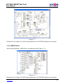
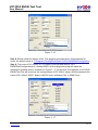
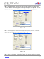
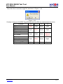
HY12P65 ENOB Test Tool User Manual . © 2012 HYCON Technology Corp. www.hycontek.com APD-DMM004-V02_EN page 1 HY12P65 ENOB Test Tool User Manual Table of Contents 1. HY12P65 ENOB TEST....................................................................................................3 1.1 SOFTWARE INTRODUCTION ............................................................................................3 1.2 SOFTWARE INSTALLATION .............................................................................................3 1.2.1 Installation ...........................................................................................................3 1.2.2 Uninstall...............................................................................................................5 1.3 ENOB AND NOISE FREE DESCRIPTION...........................................................................5 1.4 WINDOW INTERFACE .....................................................................................................6 1.4.1 OPTION .....................................................................................................................6 1.4.1.1 SETUP ...................................................................................................................7 1.4.1.2 RAM PANEL...........................................................................................................7 1.4.1.2 REG PANEL ...........................................................................................................8 1.4.1.3 ADC PANEL ...........................................................................................................8 1.4.1.4 MPN PANEL ...........................................................................................................9 1.4.1.5 POWER PANEL .....................................................................................................10 1.4.1.6 PROCOUNTER PANEL ...........................................................................................10 1.4.2 USB SCAN ............................................................................................................. 11 1.4.3 READ RAM ..............................................................................................................12 1.4.4 ENOB TEST ...........................................................................................................12 . 1.4.5 SETDMMA ............................................................................................................13 1.5 SETDMMA OPERATION PROCEDURES ........................................................................14 2. HARDWARE DESCRIPTION ........................................................................................18 2.1 COMMUNICATION STRUCTURE .....................................................................................18 2.2 USB ENOB TEST BOARD ..........................................................................................18 2.3 HY12P65 ENOB BOARD CIRCUITRY...........................................................................20 3. REVISION HISTORY.....................................................................................................21 © 2012 HYCON Technology Corp www.hycontek.com APD-DMM004-V02_EN page 2 HY12P65 ENOB Test Tool User Manual 1. HY12P65 ENOB Test 1.1 Software Introduction The main function of HY12P65 ENOB Kit is to test ADC performance of HY12P65 and to test basic DMM ranges on its software. 1.2 Software Installation 1.2.1 Installation System Requirements of operating HY12P65 ENOB Test kit: PC Hardware Request Compatible PC with PENTIUM® CPU 128 MB Memory(256MB is recommended) 10 GB Hard Disk Space OS Windows 98SE/Windows 2000/Windows XP/Windows Vista/Windows 7 Supporting x86, 32bit system; 64bit system is not supported. Applicable Interface USB Port Supporting Software Version . DMMENOBTEST V1.1 Model number in support: -HY12P65 Function items: -ENOB Test -Testing basic ranges of DMM Note: For some Windows OS, it may require to have administrator identity to install the Hex Loader to the computer. Insert the HYCON-IDE CD into the CD ROM drive and find the file in the CD ROM or file to execute Setup.exe. Following the instruction window dialogs step by step to continue setup procedures. As shown in Figure 1-1. © 2012 HYCON Technology Corp www.hycontek.com APD-DMM004-V02_EN page 3 HY12P65 ENOB Test Tool User Manual . Figure 1- 1 © 2012 HYCON Technology Corp www.hycontek.com APD-DMM004-V02_EN page 4 HY12P65 ENOB Test Tool User Manual 1.2.2 Uninstall Please remove the file of “HY12P Series ENOB Test Tool V1.1” in “Add/Remove Program” under Control Panel. 1.3 ENOB and Noise Free Description FSR In FSR RMS Noise ENOB Log 2 In2 RMS Noise Equation 1 FSR In FSR Peak - to - Peak Noise Noise Free Bits Log 2 In2 Peak - to - Peak Noise Equation 2 RMS Noise that generated from Sigma Delta ADC is the minimum voltage value of distinguishable sampling signal. Hence, ENOB (Effective Number of Bits) is calculated by RMS Noise and Full Scale Range ratio. However, RMS Noise must be calculated by many average times. Insufficient sampling times can only represent RMS Noise for a specific period of time instead of the RMS Noise of the entire ADC operation. Therefore, RMS Noise operation times cannot be less than 1024 times. . However, Noise Free Bit represents that ADC output value count is not rolling. Noise Free Bits are stable ADC output performance. Bit operation is defined as Peak-to-Peak Noise and Full Scale Range ratio. RMS Noise Calculation: n Average Counts Average ADCk k 1 n Equation 3 n = Total ADC sampling times. 2 n RMS Noise VREF ADCk Average k 1 n 2Scale Equation 4 Scale = Total ADC Output Bits Peak-to-Peak Noise Calculation: Peak - to - Peak Noise VREF ADCMax ADCMin 2Scale Equation 5 ADCMax = Maximum ADC value of total sample ADCMin = Minimum ADC value of total sample © 2012 HYCON Technology Corp www.hycontek.com APD-DMM004-V02_EN page 5 HY12P65 ENOB Test Tool User Manual 1.4 Window Interface When the software is opened, the window in below will pop up, as Figure 1- 2: Setup USB Scan Read all registers ENOB & Noise Free Test Test Ranges USB Connect Status Figure 1- 2 1.4.1 Option . Choose Option, the window will display as shown in Figure 1- 3. Set communication and IC Display RAM Panel Display Register Panel Display ADC Panel Display DMM Network Display Power Panel Display ProCounter Panel Figure 1- 3 © 2012 HYCON Technology Corp www.hycontek.com APD-DMM004-V02_EN page 6 HY12P65 ENOB Test Tool User Manual 1.4.1.1 Setup When selecting Option→Setup, a window will show as Figure 1- 4: Optical coupler Communication select Figure 1- 4 . Function Description Select Chip Select OTP IC, OTP IC program needs to burn SPI or Special communication procedures. Communication Only SPI or Special can be selected, other interfaces are not supportive. Optical Coupler When communication interface selects optical coupler to isolate channels. 1.4.1.2 RAM Panel When selecting Option→RAM Panel, a window will show as Figure 1- 5: © 2012 HYCON Technology Corp www.hycontek.com APD-DMM004-V02_EN page 7 HY12P65 ENOB Test Tool User Manual Figure 1- 5 Please refer to Chapter 3.2, RAM window operation of HY12P-IDE software user manual. 1.4.1.2 REG Panel When selecting Option→REG Panel, a window will show Figure 1- 6: . Figure 1- 6 Please refer to Chapter 3.3, REG window operation of HY12P-IDE software user manual. 1.4.1.3 ADC Panel When selecting Option→ADC Panel, a window will show Figure 1- 7: © 2012 HYCON Technology Corp www.hycontek.com APD-DMM004-V02_EN page 8 HY12P65 ENOB Test Tool User Manual Figure 1- 7 Please refer to Chapter 3.6, ADC window operation of HY12P-IDE software user manual. . 1.4.1.4 MPN Panel When selecting Option→MPN Panel, a window will show Figure 1- 8: Figure 1- 8 Please refer to Chapter 3.8, ADC window operation of HY12P-IDE software user manual. © 2012 HYCON Technology Corp www.hycontek.com APD-DMM004-V02_EN page 9 HY12P65 ENOB Test Tool User Manual 1.4.1.5 Power Panel When selecting Option→Power Panel, a window will show Figure 1- 9: . 1- 9 Figure Please refer to Chapter 3.7, ADC window operation of HY12P-IDE software user manual. 1.4.1.6 ProCounter Panel When selecting Option→ProCounter Panel, a window will show Figure 1- 10: CTA CTB CTC CTA Initial System Clock Frequenc y ENCNTI Network ENCNTI network Parameters of Cycle results status display freq. reciprocal (Cap.) Start/End Duty Figure 1- 10 © 2012 HYCON Technology Corp www.hycontek.com APD-DMM004-V02_EN page 10 HY12P65 ENOB Test Tool User Manual Function Description CTA CTA value display CTB CTB value display CTC CTC value display CTA Initial System Clock ENCNTI Network CTA Initial value setup Main frequency of System Signal input network; OFF=CMPO,ON=CNTI ENCNTI Network Status Display Display input source in accordance with ”ENCNTI” setup Parameters of Freq. Reciprocal Reciprocal of input frequency Start/End Frequency Cycle results (Cap.) Duty Start/End measurement Display freq. result Display cycle result for capacitor range measurement Display duty cycle result 1.4.2 USB Scan . USB scan function help to detect whether USB scan communication port is connected to HY12P65 ENOB Test Tool. If it is connected, the status, USB On Line, will be shown in left corner, as Figure 1- 11 displayed. Figure 1- 11 If not connected, “USB not Connect!!!” will show up as Figure 1- 12: Figure 1- 12 ※Note: 1. 2. 3. If using USB to supply power, connecting USB Line to USB ENOB Test Board (T09011 V02) can click USB Scan on the interface. If using external power supply, please connect the external power to HY12P65 ENOB Test Tool first then connecting USB Line to USB ENOB Test Board (T09011 V02) and click USB Scan on the interface. When using external power supply, please open USB ENOB Test Board (T09011 V02) J5 & J8 Jump to avoid power collide. © 2012 HYCON Technology Corp www.hycontek.com APD-DMM004-V02_EN page 11 HY12P65 ENOB Test Tool User Manual 1.4.3 Read Ram When USB port connects to HY12P65 ENOB Test Tool and ”USB On Line” is confirmed, please select Read Ram on the interface. This function will read the current RAM and register of HY12P65 to PC buffer, influencing RMS Noise & Vp-p Noise operation of ENOB Test. 1.4.4 ENOB Test After clicking ENOB Test, ENOB Test Panel will show up as Figure 1- 13: . Figure 1- 13 Function Description Sample Point ”Catch ADC” of ADC sample number, min. 32, max. 131072. It is suggested to keep as 1024. Scale Captured bit of every ADC output. Min. 8Bits, Max.19Bits ENOB Display ENOB(Effective Number of Bits), please refer to equation 1 for calculation, unit is Bit. Noise Free Display Noise Free Bits, please refer to equation 2 for calculation, unit is Bit. Average Display average of ADC sample, please refer to equation 3 for calculation, unit is Count. Vp-p Noise Display Peak-to-Peak Noise, please refer to equation 5 for calculation, unit is nV. RMS Noise Display RMS Noise, please refer to equation 4 for calculation, unit is nV. © 2012 HYCON Technology Corp www.hycontek.com APD-DMM004-V02_EN page 12 HY12P65 ENOB Test Tool User Manual Catch ADC Save to CSV Change to Chart Change FFT Ref Volt Avr. Time Real time capture and sequencing display ADC value to display zone. Store the value in display zone to HyADC.CSV file, including ENOB, Noise Free, Average & RMS Noise. Switch the value in display zone to chart Switch chart to display ”frequency domain/time domain”. Input Reference Voltage value, unit is V. Select software average, value of the display zone will be averaged according to the time set, then display to the zone again. 1.4.5 SETDMMA After clicking SETDMMA, the window will show up as Figure 1- 14: Ranges select . Route of setup file Result Display Zone Figure 1- 14 Function Description Setup file route Select the save route of setup file Range selection After the setup is done, different ranges can be tested by this function Name Calibration Unit ADC1 Scale © 2012 HYCON Technology Corp www.hycontek.com Pure character format, the input character will be the range name of “range select” Pure character format Max value (full scale) after calibration APD-DMM004-V02_EN page 13 HY12P65 ENOB Test Tool User Manual Calibration Ref. Select ADC Calibrate current ADC1 or RMS value as the input value (calibration point) Select ADC1or RMS Output as output Cal. Gain After pressing Cal. Gain, the current ADC1 or RMS output value will be calibrated as ”Calibration Ref.” setup Cal. Offset After pressing Cal. Offset, the current ADC1or RMS output value will be deemed as Offset Average Times Average ADC1or RMS output value according to the input times ADC1 Offset Display ADC1 Offset value RMS Offset Display RMS Offset value Save Register Cancel Offset Store all register status. If ”NO FILE” is selected and store is clicked, a new record will be added to this menu, utmost 10 setup files. When ticking ”Cancel Offset”, ADC1 will deduct Offset value and multiple Gain. RMS will deduct Offset first, then root and multiple Gain Result Display Zone Display results after calculation Close Close the window 1.5 SETDMMA Operation Procedures . DMM, excluding frequency that must be This function can simulate all basic ranges of measured by ProCounter. Below SETDMMA software operation procedures demonstrate the measurement of DC 600mV Step 1: Click USB Scan on the interface of HY12P65 ENOB Test Tool. “ USB On line” will show up when the connection is successful, as Figure 1- 15. If not, please make sure the hardware connection or power supply is correct. Figure 1- 15 ※Note: 1. 2. 3. If using USB to supply power, connecting USB Line to USB ENOB Test Board (T09011 V02) can click USB Scan on the interface. If using external power supply, please connect the external power to HY12P65 ENOB Test Tool first then connecting USB Line to USB ENOB Test Board (T09011 V02) and click USB Scan on the interface. When using external power supply, please open USB ENOB Test Board (T09011 V02) J5 & J8 Jump to avoid power collide. Step 2: Click Read Ram on the interface when “USB On Line” was shown, loading all registers of HY12P65 to PC buffer. Step 3: Click SETDMMA on the interface, a window as like Figure 1- 16 will pop up. © 2012 HYCON Technology Corp www.hycontek.com APD-DMM004-V02_EN page 14 HY12P65 ENOB Test Tool User Manual Figure 1- 16 Step 4: Select setup file reserve route. This program provides demo configurations for users, the default route is: C:\Program Files\HyEnobTest\HY12Px ENOBTest\Configuration Step 5: The route of DC 600mV is C:\Program . Files\HyEnobTest\HY12Px ENOBTest\Configuration\mV, clicking 600mV of the range select tag will make the information marked in blue, as shown in Figure 1- 17. At this time, the registers of HY12P65 ENOB Test Tool will be set as the configurations of DC 600mV range. And the assumed full scale of DC 600mV (ADC1 Scale) is 6600 Count, calibration Ref. is 5000 Count. Figure 1- 17 © 2012 HYCON Technology Corp www.hycontek.com APD-DMM004-V02_EN page 15 HY12P65 ENOB Test Tool User Manual Step 6: Calibration started. Input 0mV first, then click Cal. Offset and tick Cancel Offset. This time, the result zone should display 0. After input DC 500mV, click Cal. Gain. This time, the result zone should display 5000, as shown in Figure 1- 18 to finish calibration. Figure 1- 18 . Step 7: Save Configuration. Clicking Save Register after selecting the route, to store the register data as Configuration file, as shown in Figure 1- 19. Figure 1- 19 Step 8: Revise Configuration. Clicking Save Register after selecting the file to-be-covered. © 2012 HYCON Technology Corp www.hycontek.com APD-DMM004-V02_EN page 16 HY12P65 ENOB Test Tool User Manual Then click Yes to cover the origin file, as shown in Figure 1- 20. Figure 1- 20 Configure Jump on HY12P65 Target Board based on different measurement functions: Function J4 J6 & J9 J7 J3 ACV Short Open Open Open DCV AC mV Open Short Open Open DC mV Thermocouple AC Current A(Open) Open Open Open mA(1-2) DC Current uA(2-3) Resistor Continuity Open Short Open Open Diode Capacitor . Frequency(CNT Input) Open Short Short Open © 2012 HYCON Technology Corp www.hycontek.com APD-DMM004-V02_EN page 17 HY12P65 ENOB Test Tool User Manual 2. Hardware Description 2.1 Communication Structure U S B E N O B T e st B o a rd H Y 1 2 P 6 5 E N O B B o a rd PC SPI C on tro l PC sent Command or Data to USB ENOB Test Board and USB ENOB Test Board read/write SRAM Data of HYCON OTP or read/write Flash Memory. 2.2 USB ENOB Test Board 5 6 6 7 7 U9 4 5 U10 3 4 U11 2 3 . U12 1 2 T09011 V02 1 J4 Photo Input Channel J5 2 1 J8 2 1 Photo Power Photo Ground VP SPIDI_Q SPICK_Q SPIDO_Q SPICS_Q VSSP SPIIRQ_Q L1 R3 R2 R1 U6 U3 U7 2 JP1 1 JP2 VBAT J6 VSSBAT USB power Figure 2- 1 1. J2, J3: SPI communication Port J2 Description: PIN 1 VDDIN supply power to U1. If OTP external power supplies to J3, then J3 is open. If the power was supplied by USB ENOB Test Board, then J3 short. PIN 2 ICESDI_Q , DI signal line of SPI PIN 3 ICESCK_Q , CK signal line of SPI © 2012 HYCON Technology Corp www.hycontek.com APD-DMM004-V02_EN page 18 HY12P65 ENOB Test Tool User Manual PIN 4 ICESDO_Q, DO signal line of SPI PIN 5 ICECS_Q , CS signal line of CS PIN 6 VSS PIN 7 ICEIRQ_Q , signal line of detecting whether the write of HYCON OTP to Flash Memory is finished. 2. J4, J5, J8 : Optical coupler communication port J4 description PIN 1 VP, supply power to Optical coupler IC(U9~U13). To isolate the power completely, then J5 & J8 must be opened; for common power, J5 & J8 must be short circuit. PIN 2 SPIDI_Q, DI signal line of optical coupler. PIN 3 SPICK_Q, CK signal line of optical coupler. PIN 4 SPIDO_Q, DO signal line of optical coupler. PIN 5 SPICS_Q, CS signal line of optical coupler. PIN 6 VSSP, Ground of optical coupler. PIN 7 SPIIRQ_Q, signal line (optical coupler) of detecting whether the write of HYCON OTP to Flash Memory is finished. 3. J9, J10, J11 & U8 U8 is 512K byte Flash Memory . J10 & J11 is power source of Flash Memory. Using optical coupler to isolate power, then PIN1-2 of J10 & J11 must be short circuit; If no need to isolate power, then PIN2-3 of J10 & J11 must be short circuit. J9 description : PIN 1 VDD_X, supply power to U8. PIN 2 FLDI, control DI signal line of U8. PIN 3 FLCK, control CK signal line of U8. PIN 4 FLDO, control DO signal line of U8. PIN 5 FLCS, control CS signal line of U8. PIN 6 VSS_X, Ground of U8. 4. JP1, JP2, J6 & U3 JP1 & JP2 are external input power of U3, to generate VDD power. If using USB power then J6 is short circuit. Using external Power (5V), then JP1 & JP2 is input and J6 is open. U3, R1, R2 & R3 consist of a Regulator, to generate VDD power. To change output voltage, R1, R2 & R3 can be changed, its relation is given: VDD 1.240V (1 © 2012 HYCON Technology Corp www.hycontek.com R1 R 2 ) R3 APD-DMM004-V02_EN page 19 A B C D KEY3 KEY4 KEY5 KEY6 KEY2 KEY1 16 15 14 13 CMP1 12 11 10 9 CMP1 S2 1 RANGE1 SW5 Function1 SW1 1 2 3 4 5 6 7 8 1 2 3 4 24C02 A0 A1 A2 VSS U9 VDD WP SCL SDA 8 7 6 5 C8 0.1uF EEPROM HOLD1 SW6 Hz%1 SW2 IIC_SCL IIC_SDA R37 10k VDD MAX/MIN1 SW7 SW SW3 R15 20K R14 20K R13 20K R12 20K R4 20K R3 20K 20K R38 2 BACKLIGHT1 SW8 REL1 SW4 1 2 3 4 5 6 7 8 CMP0 S1 COM0 COM1 COM2 COM3 16 15 14 13 12 11 10 9 CMP0 1 2 3 4 COM0 COM1 COM2/SEG0 COM3/SEG1 J10 LCD_20*4 5 6 7 8 R2 4 3 2 1 CMP3 CMP2 CMP1 CMP0 S4 LCD_20*4 C9 10nF R36 100k VDD 功能切換 R24 0.01 R23 0.99 R22 99 AVSS C24 1UF 0.1UF C13 1UF JP3 LCD R26 10K 3 BZ 15pF C16 15pF C15 49 50 51 52 53 54 55 56 57 58 59 60 61 62 63 64 R39 1M XIN Y1 4Mhz XOUT U4 RLU PB1 PB3 C5 1UF R27 R28 ACM VDDA VGG CA CB VSS VPP/RST VDD VLCD COM0 COM1 COM2 COM3 SEG0 SEG1 SEG2 C4 0.1uF AVSS AGND BUZZER1 COM0 COM1 COM2 COM3 SEG0 SEG1 SEG2 GND RST VDD COM 3 2 3V 1 EXT VDD Sel J2 10K R25 COM 該COM點代表直接拉回AGND Current 1 2 3 J3 AVSSC14 0.1UF AVSSC11 C10 1UF 1UF C12 R48 P3 A mA P2 mA/uA uA 該COM點代表直接拉回AGND P1 COM COM VDD VDD_bat J1 Current test 1 2 R1 20K 3 CNT CMPO 2 COM1 COM3 SEG1 SEG3 SEG5 SEG7 SEG9 SEG11 SEG13 C17 R29 R30 R42 100K R41 42.2K J5 PBx C3 10uF R40 100K J4 JUMP C2 10uF C1 0.1uF PA0 PA1 PA2 PA3 PA4 PA5 PA6 RLD RLU CMP2 COM0 COM2 SEG0 SEG2 SEG4 SEG6 SEG8 SEG10 SEG12 SEG14 2 4 6 8 10 12 14 16 18 20 1 3 5 7 9 11 13 15 17 19 SEG0 SEG1 SEG2 SEG3 SEG4 SEG5 SEG6 SEG7 SEG8 SEG9 SEG10 SEG11 SEG12 SEG13 SEG14 C6 27nF R33 100 R31 HY12P65_LQFP64 J12 CNT U1 EN IN OUT ADJ 4 RLD_1 J6 J15 Power PB4 PT3.5/PB5 PT2.4/CMP0/INT24 PT2.5/CMP1/INT25 PT2.6/CMP2/INT26 PT2.7/CMP3INT27 PT3.7/CMPO PT3.6/CNT PT1.0/INT0/PSCK PT1.1/INT1/PSDI/SCE PT1.2/SDI PT1.3/RX PT1.4/TX PT1.5/SDO PT1.6/SCK PT1.7/BZ/PSDO SPI 1 3 5 7 9 11 JP4 GS2612 GND GND GND GND 4 2 4 6 8 10 12 VDD 4 3 KEY3 KEY5 KEY4 KEY2 B B 2 2 9013 Q6 9013 Q5 JP2 VSSBAT 1 VIN JP1 VBAT B B R5 Q4 9013 Q3 9013 MOV3COM TVR MOV2 TVR R34 J9 Vol/Ohm/Cap/DT JUMP PB4 PB5 CMP0 CMP1 CMP2 CMP3 CMPO KEY6 CNT KEY1 KEY2 KEY3 RX TX KEY4 KEY5 BZ HY12P65 32 31 30 29 28 27 26 25 24 23 22 21 20 19 18 17 2 2 JUMP MOV1 TVR Vol/Ohm/Cap/DT R50 PTC PTC R6 8 7 6 5 6 ON2 COM2 2 OFF2 S3 5 ON1 COM1 1 OFF1 *. POWER NET P4 Vol/Ohm/Cap/DT 1 2 3 4 1N4001 D1 R32 10M0.7% 6 5 4 3 2 1 PB0 PB1 PB2 PB3 48 47 46 45 44 43 42 41 40 39 38 37 36 35 34 33 AGND REFO PA0 PA1 PA2 PA3 PA4 PA5 PA6 RLD RLU FTN FTP PB0 PB1/PB2 PB3 1K 0.1% 2 1 10K 0.1% SEG2 SEG3 SEG4 SEG5 SEG6 SEG7 SEG8 SEG9 SEG10 SEG11 SEG12 SEG13 SEG14 SEG15 SEG16 SEG17 SEG18 SEG19 SEG20 SEG21 PB5 PB4 PB3 PB2 PB1 PB0 . 5 6 7 8 9 10 11 12 13 14 15 16 17 18 19 20 21 22 23 24 104 SEG3 SEG4 SEG5 SEG6 SEG7 SEG8 SEG9 SEG10 SEG11 SEG12 SEG13 SEG14 PT2.3/TM CKI/INT23 PT2.2/PWM/PFD/INT22 PT2.1/XTI/INT21 PT2.0/XTO/INT20 PB0 R51 PB2 RST KEY1 KEY2 BZ VDD RLD_1 IIC_SDA J7 HZ 1 2 3 4 5 6 J8 JUMP R47 該COM點代表直接拉回AGND COM SEG3 1 2 SEG4 3 SEG5 4 SEG6 5 SEG7 6 SEG8 7 SEG9 SEG10 8 SEG11 9 SEG12 10 SEG13 11 SEG14 12 IIC_SDA 1 3 IIC_SCL 1 4 XIN 15 XOUT 16 100K 1 2 3 E C 11 C 3 E 3 E C 10M 11 101K 0.1% C 1.11M 0.1% E © 2012 HYCON Technology Corp www.hycontek.com 900K 3 1 R35 CNT 1M 1UF C7 R7 VDD 5 4 3 PC817 C E PC817 P N U2 R10 500R VDD RX TX 1 2 R9 500R VDD 5 C E P N 1 2 Date: File: C Size Title IV- C19 10uF IGND Q1 R44 500R 7-May-2012 Y:\MyDesign.ddb Number D9 1N4148 D8 1N4148 D7 1N4148 D6 1N4148 6.8k R45 IV- IVD5 1N4148 D3 1N4148 1N4148 D2 IV+ C18 10uF IGND U3 R11 500R IGND 4 3 R43 10k IV+ PC_TXD PC_RXD 1N4148 D4 1 6 2 7 3 8 4 9 5 RS1 6 Sheet of Drawn By: Q2 R46 270R Photo RS232 6 Revision A B C D HY12P65 ENOB Test Tool User Manual 2.3 HY12P65 ENOB Board Circuitry APD-DMM004-V02_EN page 20 HY12P65 ENOB Test Tool User Manual 3. Revision History Version Page V01 ALL V02 17 Summary First Edition Add in the Table of Target Board Jump of different measurement functions. . © 2012 HYCON Technology Corp www.hycontek.com APD-DMM004-V02_EN page 21