1
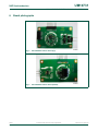
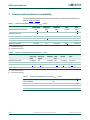
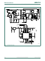
UM10731 SSL3401DB1174 7 W mains dimmable MR16/12 V driver for GU5.3 22 mm Rev. 1.1 — 14 November 2013 User manual Document information Info Content Keywords SSL3401DB1174, board version A844V0101, MR16 LED driver, mains dimmable, constant current, driver, low voltage supply, AC-to-DC conversion, LED driver Abstract This user manual describes the SSL3401 7 W dimmable MR16/12 V LED driver demo board, SSL3401DB1174. UM10731 NXP Semiconductors SSL3401DB1174 7 W MR16/12 V driver for GU5.3 22 mm Revision history Rev Date Description v. 1.1 20131114 updated issue • Modifications: v. 1 20131023 The information about component U5 in Table 7 “Bill of material” has been updated. first issue Contact information For more information, please visit: http://www.nxp.com For sales office addresses, please send an email to: [email protected] UM10731 User manual All information provided in this document is subject to legal disclaimers. Rev. 1.1 — 14 November 2013 © NXP B.V. 2013. All rights reserved. 2 of 16 UM10731 NXP Semiconductors SSL3401DB1174 7 W MR16/12 V driver for GU5.3 22 mm 1. Introduction WARNING Lethal voltage and fire ignition hazard The non-insulated high voltages that are present when operating this product, constitute a risk of electric shock, personal injury, death and/or ignition of fire. This product is intended for evaluation purposes only. It shall be operated in a designated test area by personnel qualified according to local requirements and labor laws to work with non-insulated mains voltages and high-voltage circuits. This product shall never be operated unattended. The SSL3401HN 7 W LED driver is a solution for a dimmable MR16/12 V application connected to an electronic transformer. It is dimmable with both leading edge (Triac) dimmers and trailing edge (transistor) dimmers. It generates 5.4 W output power when using a 27 V LED voltage load. The 27 V LED voltage is the voltage measured at ambient temperatures and at a 200 mA LED current. The design provides an example of how to make a driver that is suitable for small form factor LED retrofit lamps. The device controls the application to run in hysteretic boost mode. A filtered Pulse Width Modulation (PWM) signal is generated to control the analog LED current source of the application. This mode ensures an accurate LED current with low ripple. 2. Safety warnings The board must be connected to 12 V transformer. Touching the board during operation must be avoided at all times. An isolated housing is obligatory when used in uncontrolled, non-laboratory environments. The secondary circuit with LED connection has galvanic isolation using the 12 V electronic transformer. Thus galvanic isolation of the mains phase using a variable transformer is always recommended. The symbols shown in Figure 1 indicate these devices. 019aab174 019aab173 a. Isolated Fig 1. UM10731 User manual b. Not isolated Variable transformer (Variac) isolation symbols All information provided in this document is subject to legal disclaimers. Rev. 1.1 — 14 November 2013 © NXP B.V. 2013. All rights reserved. 3 of 16 UM10731 NXP Semiconductors SSL3401DB1174 7 W MR16/12 V driver for GU5.3 22 mm 3. Restrictions Connect the SSL3401HN 7 W dimmable MR16/12 V demo board to a transformer that generates a peak output voltage < 30 V. The evaluation board can drive an LED voltage of 33 V (measured LED voltage at functional current value) when the electrolytic capacitor CBUS1 (see Figure 9.) is changed to a 50 V capability and the LED current is adjusted to keep the application working within the same power range. Pay attention to the 5 V LDO (U6) dissipation and temperature when increasing the LED voltage. 4. Connecting and configuring the board The board is designed for 12 V (AC) transformer connected to a 230 V/120 V (AC), 50 Hz/60 Hz mains source. It is designed to work with multiple high-power LEDs with a total working voltage of between 24 V and 30 V. Connect the board as shown in Figure 2. 0$,16 75$16)250(5 '(02%2$5' /('/2$'%2$5' DDD Fig 2. Connecting the board The physical connection in shown in Figure 3. Fig 3. UM10731 User manual SSL3401DB1174 demo board connections All information provided in this document is subject to legal disclaimers. Rev. 1.1 — 14 November 2013 © NXP B.V. 2013. All rights reserved. 4 of 16 UM10731 NXP Semiconductors SSL3401DB1174 7 W MR16/12 V driver for GU5.3 22 mm 5. Specification Table 1 gives the specifications for the SSL3401 7 W application tested with an OSRAM HTM 70 electronic transformer unless otherwise specified. Table 1. UM10731 User manual Specifications Parameter Values Comments AC line input voltage 11 V (AC; RMS); ±15 % electronic transformer connected to 230 V mains voltage maximum input voltage 30 V input power of system (excluding electronic transformer) 7.1 W output voltage (LED voltage) minimum 24 V; typical 27 V; maximum 30 V efficiency of system (excluding electronic transformer typical: 73 % at Tamb = 25 C; board supplied by electronic transformer typical: 75 % at a PCB temperature of 100 C; board supplied by electronic transformer power factor > 0.9 Total Harmonic Distortion (THD) < 15 % output current (LED current) nominal: 200 mA LED current ripple < ±10 % dimming range 100 % to 5 % board dimensions diameter = 22 mm All information provided in this document is subject to legal disclaimers. Rev. 1.1 — 14 November 2013 board supplied by electronic transformer adjustable modifying some resistor values measured on LED current © NXP B.V. 2013. All rights reserved. 5 of 16 UM10731 NXP Semiconductors SSL3401DB1174 7 W MR16/12 V driver for GU5.3 22 mm 6. Board photographs UM10731 User manual Fig 4. SSL3401DB1174 demo board (top) Fig 5. SSL3401DB1174 demo board (bottom) All information provided in this document is subject to legal disclaimers. Rev. 1.1 — 14 November 2013 © NXP B.V. 2013. All rights reserved. 6 of 16 UM10731 NXP Semiconductors SSL3401DB1174 7 W MR16/12 V driver for GU5.3 22 mm 7. Dimmers and transformers compatibility The demo board has been tested with several electronic transformers and dimmers, as listed in Table 2 to Table 4. Table 2. Dimmers compatibility test result at Vmains = 230 V Electronic transformer Clipsal 32E450UDM Clipsal 32E450LM Clipsal 32E450TM Legrand cat 400L Legrand cat 400T Tridonic Speedy TE-0070 C101 OK[1] OK[2] OK[2] not OK OK[2] Tridonic Atco VIPER 60VA (220-240V) (EU/AU) OK[1] not OK not OK does not start OK[1] OK not OK OK OK OK Tridonic Possum 60VA OK OK[2] not OK OK OK Actec MIni60 OK OK OK OK OK not tested OK not tested OK[1] not tested ET-Redback 60VA/230-240Vac Magnetic transformer [1] Tested with two lamps. [2] Tested with three lamps. Table 3. Dimmers compatibility test result at Vmains = 230 V Electronic transformer PEHA Tronic 433 HAB Busch Universal 6591U Siemens 5TC8284 Berker 2873 (RL) GIRA 1184 00/100 Busch 6513 U-102 (RC) Magnetic transformer not tested OK not tested OK not tested not tested OSRAM HTM70/230-240 OK OK OK OK[1] OK OK Philips ET-S60 OK[1] OK[1] not OK OK[2] OK[1] OK[1] Philips Primaline 70 230-240V OK OK OK OK OK OK [1] Tested with two lamps. [2] Tested with three lamps. Table 4. Electronic transformer Lutron SPSELV 600 WH (trailing edge)[1] CB+L CV90098 OK Lightech LET 151 R 150W OK LighTech LET 60 OK Hatch VS12-60WD OK [1] UM10731 User manual Dimmers compatibility test result at Vmains = 120 V Tested with one lamp. All information provided in this document is subject to legal disclaimers. Rev. 1.1 — 14 November 2013 © NXP B.V. 2013. All rights reserved. 7 of 16 UM10731 NXP Semiconductors SSL3401DB1174 7 W MR16/12 V driver for GU5.3 22 mm $&033 %67'59% %67'59$ 9'' /('6':1 '1& )% '1& WHUPLQDO LQGH[DUHD 8. IC description '1& '1& 3$5$06(7 '1& '1& '1& 293 9'',2 '1& '1& $&035() '1& $&031 66/+1 '1& '1& /2$'3:0 ,/$7&+6(7$&7 2736(7$&7 /('3:0 '1& 966 +<676(7 +9 4) 1 '1& 5(6(7 Fig 6. DDD 7UDQVSDUHQWWRSYLHZ DDD a. Package '1& b. Pinning diagram Package description Table 5. UM10731 User manual Pin descriptions Symbol Pin Description DNC 1 do not connect RESET 2 reset if LOW DNC 3 do not connect DNC 4 do not connect DNC 5 do not connect VDD(IO) 6 3.3 V I/O supply voltage DNC 7 do not connect DNC 8 do not connect HYSTSET 9 comparator hysteresis level setting (high hysteresis level if pin is left open or set HIGH, low hysteresis level if pin is set LOW) DNC 10 do not connect DNC 11 do not connect LOADPWM 12 output load control (input pin at reset) ILATCHSETACT 13 input latching current setting control OTPSETACT 14 overtemperature setting control LEDPWM 15 LED current control (input pin at reset) DNC 16 do not connect ACMPN 17 analog comparator negative input ACMPREF 18 analog comparator reference voltage All information provided in this document is subject to legal disclaimers. Rev. 1.1 — 14 November 2013 © NXP B.V. 2013. All rights reserved. 8 of 16 UM10731 NXP Semiconductors SSL3401DB1174 7 W MR16/12 V driver for GU5.3 22 mm Table 5. UM10731 User manual Pin descriptions …continued Symbol Pin Description DNC 19 do not connect OVP 20 overvoltage protection sensing input DNC 21 do not connect PARAMSET 22 input latching current and OTP setting input DNC 23 do not connect DNC 24 do not connect DNC 25 do not connect FB 26 feedback loop input voltage DNC 27 do not connect LEDSDWN 28 LED current deep dimming control VDD 29 3.3 V supply voltage BSTDRVA 30 power MOSFET driver output BSTDRVB 31 power MOSFET driver output ACMPP 32 analog comparator positive input VSS 33 die pad ground terminal All information provided in this document is subject to legal disclaimers. Rev. 1.1 — 14 November 2013 © NXP B.V. 2013. All rights reserved. 9 of 16 UM10731 NXP Semiconductors SSL3401DB1174 7 W MR16/12 V driver for GU5.3 22 mm 9. Functional description 9.1 Latching current and OTP configuration The application can be configured for different latching currents or independently for different OTP temperature protection values. The resistor ratio RSET1/RSET2 determines the OTP threshold. By default the resistor values are: • RSET1= 47 k • RSET2 = 51 k Table 6 describes the OTP temperature threshold value versus the RSET1 resistance value when the RSET2 value is 51 k. Table 6. OTP temperature threshold versus RSET1 RSET1 value (k) OTP threshold (C) open 120 562 107.5 287 110 187 112.5 133 115 100 117.5 68.1 122.5 48.7 125 33 127.5 21.5 130 Figure 7 shows the input current of the application when the latching current is disabled, resistor RSET3 is not connected (see Section 9.2). Fig 7. UM10731 User manual Input current without latching peak All information provided in this document is subject to legal disclaimers. Rev. 1.1 — 14 November 2013 © NXP B.V. 2013. All rights reserved. 10 of 16 UM10731 NXP Semiconductors SSL3401DB1174 7 W MR16/12 V driver for GU5.3 22 mm 9.2 Adding the latched current The demo board has been built without added latched current, contrary to the IC functionality. This functionality is disabled when RSET3 is not connected (see Figure 9). To allow control of the latched current, choose an RSET3 following the information given in the data sheet. The added latched current value is linked to the resistor ratio of RSET2 and RSET3 (see Figure 9). Remark: When adding latched current, boost inductor and EMI filter inductor must have a saturation current rating above 3 A. Remark: Make sure that the maximum allowed transformer power is not exceeded when the latched current is enabled and multiple boards are connected to each transformer. 10. Board schematic /(0 - ' ' /%67 -B ' -B &(0 ' *1' 9%67 -B 9 -B *1' *1' 8 93 *1' *1' Fig 8. *1' 5(* 56 DDD Input stage UM10731 User manual All information provided in this document is subject to legal disclaimers. Rev. 1.1 — 14 November 2013 © NXP B.V. 2013. All rights reserved. 11 of 16 UM10731 NXP Semiconductors SSL3401DB1174 7 W MR16/12 V driver for GU5.3 22 mm &/(' -B -B -B '%67 9%67 -B -B 9%67 9 9 /('3 /('1 0%67 &203B,1B3/86 9 $ %67B'59 < 5% &)) 75 &%86 9 5,5() 5,&%67 03:0 &3:0) 5,5() 5,/(' 5,&%67 '3:0 53' )% 75 *1' 5/2$' 9BFXUUHQWVRXUFH 8 &)) 5% 9&& 8 538 5/2$' )% &/) &/) 5% &/' &3:0 ,/('B3:0 /2$'B3:0 5,&%67 5% /('6':1 /('6':1 %67B'59 &203B,1B3/86 9 9 8 9,1 (1 73 73 5/3 9287 )% 5/3 &+) &/3 '= '1& )% '1& /('6':1 9'' %67'59% %67'59$ 73 8 '1& '1& 3$5$06(7 '1& 293 '1& $&035() /2$'B3:0 5293 73 73 5293 $&031 ,/('B3:0 56(7 56(7 56(7 73 Fig 9. 9%67 73 73 '1& /('3:0 2736(7$&7 ,/$7&+6(7$&7 73 /2$'3:0 +<67(67 73 '1& 73 *1' '1& * 5(6(7 '1& '1& '1& 9'',2 '1& '1& '1& 73 *1' &/) $&033 *1' DDD Boost part and IC part UM10731 User manual All information provided in this document is subject to legal disclaimers. Rev. 1.1 — 14 November 2013 © NXP B.V. 2013. All rights reserved. 12 of 16 UM10731 NXP Semiconductors SSL3401DB1174 7 W MR16/12 V driver for GU5.3 22 mm 11. Bill Of Material (BOM) Table 7. Bill of material Reference Description and values Part number Manufacturer CBUS1 capacitor; 330 F; 35 V; 10 mm 12.5 mm EEUFR1V331U Panasonic CEM2 capacitor; 1 F; 50 V; 125 C; 10 %; X7R; 0805 GRM21BR71H105KA12L Murata CFF1; CFF2 capacitor; 33 pF; 50 V; 125 C; 5 %; 0603 GRM1885C1H330JA01D Murata CLD1; CLF1; CPWMF1 capacitor; 100 nF; 50 V; 125 C; 10 %; 0603 GRM188R71H104KA93D Murata CHF1; CLF2; CPWM1 capacitor; 1 F; 16 V; 125 C; 10 %; X7R; 0603 0603YC105KAT2A AVX CLF4 capacitor; not connected; 0805 - - CLP1 capacitor; 33 nF; 50 V; 125 C; 5 %; 0603 06035C333JAT2A AVX B360A-13-F Diodes Incorporated D2; D3; D4; diode; rectifier; 60 V; 3 A; 150 C; SMA D5 DBST1 diode; rectifier; 60 V; 1 A; 150 C; SMA SS19L Taiwan Semiconductor DPWM1 shunt regulator; 2.5 V; 0.5 %; SOT23 TL431BMFDT NXP Semiconductors DZ1 Zener diode; 3.3 V; 0.5 W; SOD323 TDZ3V3J NXP Semiconductors LBST1 inductor; 15 H; 2.3 A; 125 C; 20 %; 6 mm SRN6045-150M Bourns LEM1 inductor; 4.7 F; 1.7 A; 125 C; 20 %; 4.5 mm SDR0403-4R7ML Bourns MBST1 N MOSFET; 60 V; 12 A; 150 C; DFN2020-6 PMPB40SNA NXP Semiconductors MH1; MH2; MH3; MH4 strut; M3 25 mm 301 3150 400 50 Ex-ACME MPWM1 N/P MOSFET; 60 V; 330 mA; 50 V; 170 mA; 150 C; SOT366 NX1029X NXP Semiconductors RB1 resistor; 9.1 k; 150 V; 155 C; 1 %; 0805 CRCW08059K10FKEA Vishay RB2 resistor; 698 ; 75 V; 155 C; 100 mW; 1 %; 0603 CRCW0603698RFKEA Vishay RB3; RB4 resistor; 220 k; 50 V; 155 C; 1 %; 0603 CRCW0603220KFKEA Vishay RICBST1 resistor; 1 ; leaded 7 mm 2.5 mm MRS25000C1008FCT00 Vishay RICBST2; RICBST3 resistor; 0.51 ; 1 %; 0.5 W; 1206 CRM1206-FX-R510ELF Bourns RILED1 resistor; 2 ; 250 mW; 100 ppm; 125 C; 1 %; 1206 ERJ6BQF2R0V Panasonic RIREF1 resistor; 24 k; 50 V; 100 ppm; 155 C; 1 %; 0603 MC 0.063W 0603 1% 24K Multicomp RIREF2 resistor; 6.65 k; 100 ppm; 125 C; 1 %; 0603 CRCW06036K65FKEA Vishay RLOAD1; RLOAD2 resistor; 910 ; 330 mW; 200 ppm; 125 C; 5 %; 1206 ERJP08F9100V Panasonic RLP1 resistor; 15 k; 100 ppm; 125 C; 1 %; 0603 CPF0603B15KE1 TE Connectivity RLP2 resistor; 5.1 k; 100 ppm; 125 C; 1 %; 0603 CRCW06035K10FKEA Vishay ROVP1 resistor; 100 k; 100 ppm; 155 C; 1 %; 0402 CPF0402B100KE1 TE Connectivity ROVP2 resistor; 4.99 k; 60 V; 50 ppm; 125 C; 1 %; 0603 CPF0603F4K99C1 TE Connectivity RPU1; RPD1 resistor; 10 k; 75 V; 100 ppm; 125 C; 1 %; 0603 CRCW060310K0FKEA Vishay RS1 resistor; 0.5 ; 100 ppm; 155 C; 1 %; 0603 LRCS0603-0R5FT5 Welwyn Components UM10731 User manual All information provided in this document is subject to legal disclaimers. Rev. 1.1 — 14 November 2013 © NXP B.V. 2013. All rights reserved. 13 of 16 UM10731 NXP Semiconductors SSL3401DB1174 7 W MR16/12 V driver for GU5.3 22 mm Table 7. Bill of material …continued Reference Description and values Part number Manufacturer RSET1 resistor; 48.7 k; 100 ppm; 155 C; 1 %; 0402 CRCW040248K7FKED Vishay RSET2 resistor; 51 k; 60 V; 50 ppm; 155 C; 1 %; 0402 CRCW040251K0FKED Vishay RSET3 resistor; not connected; 0402 - - U1 IC; NPN/PNP; 20 V; 6.3 A; 800 mW; SOT96-1 PBSS4021SPN NXP Semiconductors U2 IC; 3.3 V regulator; 150 mA; 3 %; DFN1010C-4 LD6805K/33H NXP Semiconductors U4 IC; driver; HVQFN33 SSL3401HN NXP Semiconductors U5 IC; single inverter buffer; 5 V; 24 mA; TSSOP5 74LVC1G14GW-Q100 NXP Semiconductors U6 IC; 5 V regulator; 100 mA; 5 %; SOT223 TDA3664/N1 NXP Semiconductors UM10731 User manual All information provided in this document is subject to legal disclaimers. Rev. 1.1 — 14 November 2013 © NXP B.V. 2013. All rights reserved. 14 of 16 UM10731 NXP Semiconductors SSL3401DB1174 7 W MR16/12 V driver for GU5.3 22 mm 12. Legal information 12.1 Definitions Draft — The document is a draft version only. The content is still under internal review and subject to formal approval, which may result in modifications or additions. NXP Semiconductors does not give any representations or warranties as to the accuracy or completeness of information included herein and shall have no liability for the consequences of use of such information. Export control — This document as well as the item(s) described herein may be subject to export control regulations. Export might require a prior authorization from competent authorities. 12.2 Disclaimers Limited warranty and liability — Information in this document is believed to be accurate and reliable. However, NXP Semiconductors does not give any representations or warranties, expressed or implied, as to the accuracy or completeness of such information and shall have no liability for the consequences of use of such information. NXP Semiconductors takes no responsibility for the content in this document if provided by an information source outside of NXP Semiconductors. In no event shall NXP Semiconductors be liable for any indirect, incidental, punitive, special or consequential damages (including - without limitation - lost profits, lost savings, business interruption, costs related to the removal or replacement of any products or rework charges) whether or not such damages are based on tort (including negligence), warranty, breach of contract or any other legal theory. Notwithstanding any damages that customer might incur for any reason whatsoever, NXP Semiconductors’ aggregate and cumulative liability towards customer for the products described herein shall be limited in accordance with the Terms and conditions of commercial sale of NXP Semiconductors. Right to make changes — NXP Semiconductors reserves the right to make changes to information published in this document, including without limitation specifications and product descriptions, at any time and without notice. This document supersedes and replaces all information supplied prior to the publication hereof. Suitability for use — NXP Semiconductors products are not designed, authorized or warranted to be suitable for use in life support, life-critical or safety-critical systems or equipment, nor in applications where failure or malfunction of an NXP Semiconductors product can reasonably be expected to result in personal injury, death or severe property or environmental damage. NXP Semiconductors and its suppliers accept no liability for inclusion and/or use of NXP Semiconductors products in such equipment or applications and therefore such inclusion and/or use is at the customer’s own risk. Applications — Applications that are described herein for any of these products are for illustrative purposes only. NXP Semiconductors makes no representation or warranty that such applications will be suitable for the specified use without further testing or modification. Customers are responsible for the design and operation of their applications and products using NXP Semiconductors products, and NXP Semiconductors accepts no liability for any assistance with applications or customer product design. It is customer’s sole responsibility to determine whether the NXP Semiconductors product is suitable and fit for the customer’s applications and products planned, as well as for the planned application and use of customer’s third party customer(s). Customers should provide appropriate design and operating safeguards to minimize the risks associated with their applications and products. UM10731 User manual NXP Semiconductors does not accept any liability related to any default, damage, costs or problem which is based on any weakness or default in the customer’s applications or products, or the application or use by customer’s third party customer(s). Customer is responsible for doing all necessary testing for the customer’s applications and products using NXP Semiconductors products in order to avoid a default of the applications and the products or of the application or use by customer’s third party customer(s). NXP does not accept any liability in this respect. Evaluation products — This product is provided on an “as is” and “with all faults” basis for evaluation purposes only. NXP Semiconductors, its affiliates and their suppliers expressly disclaim all warranties, whether express, implied or statutory, including but not limited to the implied warranties of non-infringement, merchantability and fitness for a particular purpose. The entire risk as to the quality, or arising out of the use or performance, of this product remains with customer. In no event shall NXP Semiconductors, its affiliates or their suppliers be liable to customer for any special, indirect, consequential, punitive or incidental damages (including without limitation damages for loss of business, business interruption, loss of use, loss of data or information, and the like) arising out the use of or inability to use the product, whether or not based on tort (including negligence), strict liability, breach of contract, breach of warranty or any other theory, even if advised of the possibility of such damages. Notwithstanding any damages that customer might incur for any reason whatsoever (including without limitation, all damages referenced above and all direct or general damages), the entire liability of NXP Semiconductors, its affiliates and their suppliers and customer’s exclusive remedy for all of the foregoing shall be limited to actual damages incurred by customer based on reasonable reliance up to the greater of the amount actually paid by customer for the product or five dollars (US$5.00). The foregoing limitations, exclusions and disclaimers shall apply to the maximum extent permitted by applicable law, even if any remedy fails of its essential purpose. Safety of high-voltage evaluation products — The non-insulated high voltages that are present when operating this product, constitute a risk of electric shock, personal injury, death and/or ignition of fire. This product is intended for evaluation purposes only. It shall be operated in a designated test area by personnel that is qualified according to local requirements and labor laws to work with non-insulated mains voltages and high-voltage circuits. The product does not comply with IEC 60950 based national or regional safety standards. NXP Semiconductors does not accept any liability for damages incurred due to inappropriate use of this product or related to non-insulated high voltages. Any use of this product is at customer’s own risk and liability. The customer shall fully indemnify and hold harmless NXP Semiconductors from any liability, damages and claims resulting from the use of the product. Translations — A non-English (translated) version of a document is for reference only. The English version shall prevail in case of any discrepancy between the translated and English versions. 12.3 Trademarks Notice: All referenced brands, product names, service names and trademarks are the property of their respective owners. All information provided in this document is subject to legal disclaimers. Rev. 1.1 — 14 November 2013 © NXP B.V. 2013. All rights reserved. 15 of 16 UM10731 NXP Semiconductors SSL3401DB1174 7 W MR16/12 V driver for GU5.3 22 mm 13. Contents 1 2 3 4 5 6 7 8 9 9.1 9.2 10 11 12 12.1 12.2 12.3 13 Introduction . . . . . . . . . . . . . . . . . . . . . . . . . . . . 3 Safety warnings . . . . . . . . . . . . . . . . . . . . . . . . . 3 Restrictions . . . . . . . . . . . . . . . . . . . . . . . . . . . . 4 Connecting and configuring the board . . . . . . 4 Specification. . . . . . . . . . . . . . . . . . . . . . . . . . . . 5 Board photographs . . . . . . . . . . . . . . . . . . . . . . 6 Dimmers and transformers compatibility . . . . 7 IC description . . . . . . . . . . . . . . . . . . . . . . . . . . . 8 Functional description . . . . . . . . . . . . . . . . . . 10 Latching current and OTP configuration . . . . . 10 Adding the latched current . . . . . . . . . . . . . . . 11 Board schematic . . . . . . . . . . . . . . . . . . . . . . . 11 Bill Of Material (BOM) . . . . . . . . . . . . . . . . . . . 13 Legal information. . . . . . . . . . . . . . . . . . . . . . . 15 Definitions . . . . . . . . . . . . . . . . . . . . . . . . . . . . 15 Disclaimers . . . . . . . . . . . . . . . . . . . . . . . . . . . 15 Trademarks. . . . . . . . . . . . . . . . . . . . . . . . . . . 15 Contents . . . . . . . . . . . . . . . . . . . . . . . . . . . . . . 16 Please be aware that important notices concerning this document and the product(s) described herein, have been included in section ‘Legal information’. © NXP B.V. 2013. All rights reserved. For more information, please visit: http://www.nxp.com For sales office addresses, please send an email to: [email protected] Date of release: 14 November 2013 Document identifier: UM10731