1
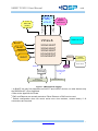
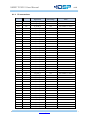
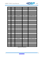
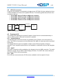
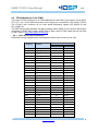
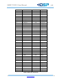
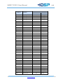
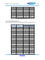
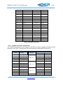
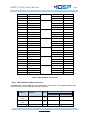
UM027 FC6301 User Manual r1.3 FC6301 User Manual 4DSP LLC, USA Email: [email protected] This document is the property of 4DSP LLC and may not be copied nor communicated to a third party without the written permission of 4DSP LLC UM027 © 4DSP LLC 2013 www.4dsp.com -1- UM027 FC6301 User Manual r1.3 Revision History Date Revision Revision 2010-10-05 Draft 0.1 2010-11-21 Release 1.0 2013-04-08 Added the FMC pinout tables 1.1 2013-05-01 Updated Table 5: FMC GTX/GTH connections to use the MGTx_abc notation. Also fixed wrong 1.2 reference to MGT bank 115 and changed it to MGT bank 113 2014-04-15 UM027 Added “Table 2: P2 connections” and updated section 4.1 with a description of the P2 connector limitation. www.4dsp.com 1.3 -2- UM027 FC6301 User Manual r1.3 Table of Contents 1 2 3 4 5 6 7 8 Acronyms and related documents ............................................................................. 5 1.1 Acronyms ................................................................................................................ 5 1.2 Related Documents ................................................................................................. 6 General description ..................................................................................................... 6 Installation ................................................................................................................... 8 3.1 Requirements and handling instructions .................................................................. 8 3.2 Firmware and Software ........................................................................................... 8 Hardware Specification ............................................................................................... 8 4.1 Phycisal specifications ............................................................................................ 8 4.1.1 Front panel layout ............................................................................................ 8 4.2 cPCI P0 connector .................................................................................................. 9 4.3 Front panel IO ........................................................................................................11 4.3.1 Gigabit Ethernet ..............................................................................................11 4.3.2 UART ..............................................................................................................11 4.3.3 LED .................................................................................................................11 4.4 FPGA Mezzanine Card (FMC) ...............................................................................12 4.4.1 Bank A (LA, HA) connections ..........................................................................12 4.4.2 Bank B (HB) connections ................................................................................15 4.4.3 Gigabit transceiver connections ......................................................................16 4.4.4 Miscellaneous FMC connections .....................................................................17 4.5 SPI flash.................................................................................................................18 4.6 Virtex-6 FPGA device .............................................................................................18 4.7 BLAST sites ...........................................................................................................19 4.8 Clock tree ...............................................................................................................19 4.8.1 FMC GTX Reference Clock .............................................................................20 4.8.2 FMC Clock connections ..................................................................................20 4.9 FPGA device configuration .....................................................................................21 4.9.1 Flash storage ..................................................................................................21 4.9.2 CPLD device ...................................................................................................21 4.9.3 DIP Switch ......................................................................................................21 4.9.4 CPLD LEDs and board status .........................................................................22 4.9.5 JTAG...............................................................................................................22 4.10 Power supply ......................................................................................................23 4.11 Hotswap .............................................................................................................24 4.12 Power and temperature monitor..........................................................................24 Environment................................................................................................................26 5.1 Temperature ..........................................................................................................26 5.2 Convection cooling .................................................................................................26 Safety...........................................................................................................................26 EMC .............................................................................................................................26 Warranty ......................................................................................................................26 UM027 www.4dsp.com -3- UM027 FC6301 User Manual r1.3 Appendix A: Errata .............................................................................................................27 UM027 www.4dsp.com -4- UM027 FC6301 User Manual r1.3 1 Acronyms and related documents 1.1 Acronyms A/D Analog to Digital Converter BLAST Board Level Advanced Scalable Technology CPLD Complex Programmable Logic Device D/A Digital to Analog Converter DCI Digitally Controlled Impedance DDR Double Data Rate DSP Digital Signal Processing FBGA Fineline Ball Grid Array FFT Fast Fourier Transformation FMC FPGA Mezzanine Card FPDP Front Panel Data Port FPGA Field Programmable Gate Array GPIO General Purpose Input/Output GUI Graphical User Interface HPC High pin count IP Intellectual Property JTAG Join Test Action Group LED Light Emitting Diode LSB Least Significant Bit(s) LVDS Low Voltage Differential Signaling LVTTL Low Voltage Transistor Logic level MGT Multi-Gigabit Transceiver MSB Most Significant Bit(s) PCB Printed Circuit Board PCI Peripheral Component Interconnect PCIe PCI Express PLL Phase Locked Loop pps Pulse Per Second QDR Quadruple Data rate SDRAM Synchronous Dynamic Random Access memory sFPDP Serial FPDP SPI Serial Peripheral Interconnect SRAM Synchronous Random Access memory SRIO Serial Input/Output SSC Spread Spectrum Clocking TTL Transistor Logic level UART Universal Asynchronous Receiver/Transmitter USB Universal Serial Bus Table 1: Glossary UM027 www.4dsp.com -5- UM027 FC6301 User Manual 1.2 r1.3 Related Documents 3U CompactPCI specifications (PICMG 2.0 R3.0) CompactPCI Hot Swap specifications (PICMG 2.1 R2.0) VITA 57.1 FPGA Mezzanine Card Standard Xilinx Virtex-6 documentation 2 General description The FC6301 is a high performance CompactPCI (cPCI) card with advanced digital signal processing capabilities. The design has been targeted for customer programmable implementations of complex FPGA algorithms for Digital Signal Processing (DSP) applications. The FC6301 product is in the 3U cPCI form factor, offering various direct onboard interface options that are closely coupled to large - fast on-board memory resources of the Xilinx Virtex™-6 FPGA. The FC6301 is an excellent choice for high performance applications that require the use of accelerated frequency-domain algorithms such as with FFTs. 4DSP has many off-the-shelf Intellectual Property (IP) cores for applications that require the highest level of performance. CompactPCI (cPCI) is an adaptation of the Peripheral Component Interconnect (PCI) Specification for industrial and military embedded applications requiring a more robust mechanical form factor than a desktop PC. UM027 www.4dsp.com -6- UM027 FC6301 User Manual r1.3 Optional FMC3 Optional Gigabit 3 Ethernet 2x 160 single ended 80 LVDS pairs 10x MGT 3.125Gbps VITA 57 optional Mini USB (UART) Virtex-6 BLAST1 128Mbit SPI flash2 XC6VLX240T XC6VLX365T XC6VLX550T XC6VSX315T XC6VSX475T BLAST BLAST BLAST CPLD 512Mbit parallel flash CPLD LED x4 JTAG PCIe x1 PCIe x1 to PCI bridge cPCI J1 32-bit 33/66MHz 72 single-ended user defined IO4 cPCI J2 user I/O Figure 1: FMC122 block diagram 1 th 4 BLAST site only fully supported on SX475T and LX550T devices, on other devices only the DDR2 BLAST (A) is supported. 2 Refer to the Appendix for Errata. 3 FMC and Ethernet are mutually exclusive. Either Ethernet or FMC can be used. 4 Default configuration does not mount series zero ohm resistors, contact factory if J2 connections are required. UM027 www.4dsp.com -7- UM027 FC6301 User Manual r1.3 3 Installation 3.1 Requirements and handling instructions The FC6301 daughter card must be installed cPCI backplane compliant to the cPCI standard. Do not flex the board and prevent electrostatic discharges by observing ESD precautions when handling the card. 3.2 Firmware and Software Drivers, API libraries and a program example working in combination with a pre-programmed firmware for the FPGA is provided. The FC6301 is delivered with an interface to the Xilinx PCIexpress endpoint in the Virtex-6 device and an example VHDL design so users can start performing data transfers over the PCI bus right out of the box. For more information about software installation and FPGA firmware, please refer the 4FM Get Started Guide. 4 Hardware Specification 4.1 Phycisal specifications The FC6301 card complies with the compact PCI standard known as PICMG 2.0 R3.0. The card is a 3U (100 mm by 160 mm) module which incorporates a 32 bits PCI bus on the P1 connector. The P2 connector is fully routed to the Virtex6 FPGA through zero ohm resistors. However the LX240T version of the Virtex6 FPGA does not completely support the P2 connector. Table 2 lists the signals the connections of P2 and which signals are not available on the LX240T. Also addition: the zero ohm resistors are not mounted by default, contact factory in case connections on P2 are required. 4.1.1 Front panel layout There are three front panel options. One front panel is used when an FMC board is mounted. The other front panel is used when the Ethernet IO option is chosen. And the third option has no cutout at all. Figure 2: FMC option Bezel drawing UM027 www.4dsp.com -8- UM027 FC6301 User Manual 4.1.2 P2 connections FPGA Pin UM027 r1.3 P2 pin # Signal name Bank Voltage Notes AT26 A1 FP_RTM_0 1.8V Not available on LX240T AU27 A2 FP_RTM_1 1.8V Not available on LX240T AK23 B6 FP_RTM_10 1.8V Not available on LX240T BB26 B8 FP_RTM_11 1.8V Not available on LX240T BB27 B10 FP_RTM_12 1.8V Not available on LX240T AM23 C1 FP_RTM_13 1.8V Not available on LX240T AN23 C3 FP_RTM_14 1.8V Not available on LX240T AU23 C4 FP_RTM_15 1.8V Not available on LX240T AU24 C6 FP_RTM_16 1.8V Not available on LX240T AP25 C8 FP_RTM_17 1.8V Not available on LX240T AP26 C10 FP_RTM_18 1.8V Not available on LX240T AK24 D1 FP_RTM_19 1.8V Not available on LX240T AK22 A3 FP_RTM_2 1.8V Not available on LX240T AL25 D2 FP_RTM_20 1.8V Not available on LX240T AP23 D3 FP_RTM_21 1.8V Not available on LX240T AR23 D5 FP_RTM_22 1.8V Not available on LX240T AM24 D7 FP_RTM_23 1.8V Not available on LX240T AL24 D9 FP_RTM_24 1.8V Not available on LX240T BA25 D11 FP_RTM_25 1.8V Not available on LX240T AN24 E1 FP_RTM_26 1.8V Not available on LX240T AN25 E2 FP_RTM_27 1.8V Not available on LX240T AV26 E3 FP_RTM_28 1.8V Not available on LX240T AU26 E4 FP_RTM_29 1.8V Not available on LX240T AJ22 A7 FP_RTM_3 1.8V Not available on LX240T AR24 E5 FP_RTM_30 1.8V Not available on LX240T AT24 E6 FP_RTM_31 1.8V Not available on LX240T AW25 E7 FP_RTM_32 1.8V Not available on LX240T AW26 E8 FP_RTM_33 1.8V Not available on LX240T AT25 E9 FP_RTM_34 1.8V Not available on LX240T AR25 E10 FP_RTM_35 1.8V Not available on LX240T H24 A12 FP_RTM_36 1.8V Not available on LX240T G24 A13 FP_RTM_37 1.8V Not available on LX240T E27 A14 FP_RTM_38 1.8V Not available on LX240T D27 A15 FP_RTM_39 1.8V Not available on LX240T AY27 A8 FP_RTM_4 1.8V Not available on LX240T F25 A16 FP_RTM_40 1.8V Not available on LX240T F24 A17 FP_RTM_41 1.8V Not available on LX240T C28 A18 FP_RTM_42 1.8V Not available on LX240T B28 A19 FP_RTM_43 1.8V Not available on LX240T www.4dsp.com -9- UM027 FC6301 User Manual r1.3 H26 A20 FP_RTM_44 1.8V Not available on LX240T G26 A21 FP_RTM_45 1.8V Not available on LX240T F26 B12 FP_RTM_46 1.8V Not available on LX240T K25 B14 FP_RTM_47 1.8V Not available on LX240T J25 B16 FP_RTM_48 1.8V Not available on LX240T B27 B18 FP_RTM_49 1.8V Not available on LX240T AW27 A9 FP_RTM_5 1.8V Not available on LX240T A27 B19 FP_RTM_50 1.8V Not available on LX240T J23 B20 FP_RTM_51 1.8V Not available on LX240T K23 C12 FP_RTM_52 1.8V Not available on LX240T M19 C14 FP_RTM_53 1.8V Not available on LX240T N19 C15 FP_RTM_54 1.8V Not available on LX240T N21 C16 FP_RTM_55 1.8V Not available on LX240T M21 C17 FP_RTM_56 1.8V Not available on LX240T A26 C18 FP_RTM_57 1.8V Not available on LX240T A25 C19 FP_RTM_58 1.8V Not available on LX240T C26 C20 FP_RTM_59 1.8V Not available on LX240T AM22 A10 FP_RTM_6 1.8V Not available on LX240T D26 C21 FP_RTM_60 1.8V Not available on LX240T M22 D13 FP_RTM_61 1.8V Not available on LX240T B26 D15 FP_RTM_62 1.8V Not available on LX240T C25 D17 FP_RTM_63 1.8V Not available on LX240T N23 D19 FP_RTM_64 1.8V Not available on LX240T M24 D21 FP_RTM_65 1.8V Not available on LX240T D25 E11 FP_RTM_66 1.8V Not available on LX240T E25 E12 FP_RTM_67 1.8V Not available on LX240T P21 E13 FP_RTM_68 1.8V Not available on LX240T P22 E14 FP_RTM_69 1.8V Not available on LX240T AL22 A11 FP_RTM_7 1.8V Not available on LX240T P20 E15 FP_RTM_70 1.8V Not available on LX240T N20 B21 FP_RTM_71 1.8V Not available on LX240T BA26 B2 FP_RTM_8 1.8V Not available on LX240T AJ23 B4 FP_RTM_9 1.8V Not available on LX240T K42 A6 FP_RTM_CLKinn 2.5V J42 A5 FP_RTM_CLKinp 2.5V P31 E21 FP_RTM_CLKoutn 2.5V P30 E20 FP_RTM_CLKoutp 2.5V Table 2: P2 connections UM027 www.4dsp.com - - 10 UM027 FC6301 User Manual 4.2 r1.3 cPCI P0 connector 1 32 bits PCI 33 or 66 MHz PI7C9X110 cPCI-P1 1 Virtex6 PCIexpress 1 lane A one lane PCI express is connected to a bridge device (PI7C9X110) thus making the Virtex6 FPGA available for access on the parallel PCI bus. The following performances have been recorded on the bus. PCI 33 MHz: Host to FC6301 60 Mbytes/s sustained PCI 33 MHz: FC6301 to Host 110 Mbytes/s sustained PCI 66 MHz: Host to FC6301 120 Mbytes/s sustained PCI 66 MHz: FC6301 to Host 140 Mbytes/s sustained Figure 3 : PCI interface diagram 4.3 Front panel IO The FC6301 offers different front panel IO options. Not all can be used simultaneously. In case an FMC is used no Ethernet connection is possible. 4.3.1 Gigabit Ethernet Two Ethernet ports (RJ45 connectors) are available on the FC6301 in the front panel I/O area. The FPGA is connected to a 2-port Ethernet PHY (88E1121) that connects to two RJ45 connectors. The Gigabit Ethernet ports are capable to adapt to lower Ethernet speeds (10/100) if required. This is a specific option which is not available in combination with an FMC daughter card. 4.3.2 UART One UART connection will be available on the fontanel via a mini USB connection. The serial interface is made using a USB to UART Bridge (CP2102). The UART will connect directly to the Virtex 6 FPGA via a level translator. 4.3.3 LED Four LEDs are connected to the CPLD and are available in the front panel I/O area UM027 www.4dsp.com - - 11 UM027 FC6301 User Manual 4.4 r1.3 FPGA Mezzanine Card (FMC) The Virtex-6 FPGA interfaces to an FPGA Mezzanine Card (FMC) via a high pin count (HPC) VITA 57.1 site. All the differential and control signals are connected to the Virtex-6 FPGA. The FC6301 also connects all ten high speed differential signals (DP_M2C[9..0] and DP_C2M[9..0]). The FMC site provides flexibility for adding analog and/or digital IO via customer developed, third party or 4DSP FMC boards. 4DSP offers a wide variety of FMC cards that can be used on the FC6301: http://www.4dsp.com/fmc.php 4.4.1 Bank A (LA, HA) connections Differential routing is applied with matched delay within pairs on bank A (LA, HA). FMC HPC FPGA Pin Net Name Pin Number UM027 Pin Name AF30 LA_N00_CC G7 LA00_N_CC AE30 LA_P00_CC G6 LA00_P_CC AK37 LA_N01_CC D9 LA01_N_CC AJ37 LA_P01_CC D8 LA01_P_CC AK30 LA_N02 H8 LA02_N AJ31 LA_P02 H7 LA02_P AJ32 LA_N03 G10 LA03_N AK33 LA_P03 G9 LA03_P AG29 LA_N04 H11 LA04_N AH29 LA_P04 H10 LA04_P AG39 LA_N05 D12 LA05_N AF39 LA_P05 D11 LA05_P AG37 LA_N06 C11 LA06_N AF37 LA_P06 C10 LA06_P AG33 LA_N07 H14 LA07_N AF32 LA_P07 H13 LA07_P AF41 LA_N08 G13 LA08_N AF42 LA_P08 G12 LA08_P AE42 LA_N09 D15 LA09_N AD42 LA_P09 D14 LA09_P AD38 LA_N10 C15 LA10_N AE38 LA_P10 C14 LA10_P AD30 LA_N11 H17 LA11_N AD31 LA_P11 H16 LA11_P Y39 LA_N12 G16 LA12_N Y40 LA_P12 G15 LA12_P AA39 LA_N13 D18 LA13_N Y38 LA_P13 D17 LA13_P www.4dsp.com - - 12 UM027 FC6301 User Manual r1.3 Y37 LA_N14 C19 LA14_N W37 LA_P14 C18 LA14_P Y35 LA_N15 H20 LA15_N AA35 LA_P15 H19 LA15_P AA30 LA_N16 G19 LA16_N Y30 LA_P16 G18 LA16_P AB31 LA_N17_CC D21 LA17_N_CC AA31 LA_P17_CC D20 LA17_P_CC V30 LA_N18_CC C23 LA18_N_CC W30 LA_P18_CC C22 LA18_P_CC Y33 LA_N19 H23 LA19_N W32 LA_P19 H22 LA19_P Y42 LA_N20 G22 LA20_N W42 LA_P20 G21 LA20_P W31 LA_N21 H26 LA21_N V31 LA_P21 H25 LA21_P W33 LA_N22 G25 LA22_N V33 LA_P22 G24 LA22_P W41 LA_N23 D24 LA23_N V41 LA_P23 D23 LA23_P W40 LA_N24 H29 LA24_N V40 LA_P24 H28 LA24_P W38 LA_N25 G28 LA25_N V38 LA_P25 G27 LA25_P V36 LA_N26 D27 LA26_N W36 LA_P26 D26 LA26_P V35 LA_N27 C27 LA27_N W35 LA_P27 C26 LA27_P U41 LA_N28 H32 LA28_N U42 LA_P28 H31 LA28_P V39 LA_N29 G31 LA29_N U39 LA_P29 G30 LA29_P U38 LA_N30 H35 LA30_N U37 LA_P30 H34 LA30_P U34 LA_N31 G34 LA31_N V34 LA_P31 G33 LA31_P U33 LA_N32 H38 LA32_N U32 LA_P32 H37 LA32_P T32 LA_N33 G37 LA33_N R32 LA_P33 G36 LA33_P Table 3: FMC LA connections UM027 www.4dsp.com - - 13 UM027 FC6301 User Manual r1.3 FMC HPC FPGA Pin Net Name Pin Number UM027 Pin Name AE32 HA_N00_CC F5 HA00_N_CC AD32 HA_P00_CC F4 HA00_P_CC AJ35 HA_N01_CC E3 HA01_N_CC AH34 HA_P01_CC E2 HA01_P_CC AM42 HA_N02 K8 HA02_N AL42 HA_P02 K7 HA02_P AM41 HA_N03 J7 HA03_N AL41 HA_P03 J6 HA03_P AL40 HA_N04 F8 HA04_N AK40 HA_P04 F7 HA04_P AL39 HA_N05 E7 HA05_N AK39 HA_P05 E6 HA05_P AJ40 HA_N06 K11 HA06_N AH39 HA_P06 K10 HA06_P AH41 HA_N07 J10 HA07_N AG42 HA_P07 J9 HA07_P AG41 HA_N08 F11 HA08_N AF40 HA_P08 F10 HA08_P AF36 HA_N09 E10 HA09_N AF35 HA_P09 E9 HA09_P AF34 HA_N10 K14 HA10_N AG34 HA_P10 K13 HA10_P AD41 HA_N11 J13 HA11_N AC41 HA_P11 J12 HA11_P AE39 HA_N12 F14 HA12_N AE40 HA_P12 F13 HA12_P AE35 HA_N13 E13 HA13_N AE34 HA_P13 E12 HA13_P AD33 HA_N14 J16 HA14_N AE33 HA_P14 J15 HA14_P AC33 HA_N15 F17 HA15_N AC34 HA_P15 F16 HA15_P AD40 HA_N16 E16 HA16_N AC40 HA_P16 E15 HA16_P AD37 HA_N17_CC K17 HA17_N_CC AE37 HA_P17_CC K16 HA17_P_CC AB38 HA_N18_CC J19 HA18_N AB37 HA_P18_CC J18 HA18_P www.4dsp.com - - 14 UM027 FC6301 User Manual r1.3 AB36 HA_N19 F20 HA19_N AC36 HA_P19 F19 HA19_P AB33 HA_N20 E19 HA20_N AB32 HA_P20 E18 HA20_P AB42 HA_N21 K20 HA21_N AA42 HA_P21 K19 HA21_P AB41 HA_N22 J22 HA22_N AA41 HA_P22 J21 HA22_P AA40 HA_N23 K23 HA23_N AB39 HA_P23 K22 HA23_P Table 4: FMC HA connections 4.4.2 Bank B (HB) connections Differential routing is applied with matched delay within all pairs on bank B (HB). FMC HPC FPGA Pin Net Name Pin Number UM027 Pin Name P38 HB_N00_CC K26 HB00_N_CC R39 HB_P00_CC K25 HB00_P_CC M37 HB_N01 J25 HB01_N M36 HB_P01 J24 HB01_P L40 HB_N02 F23 HB02_N L39 HB_P02 F22 HB02_P M39 HB_N03 E22 HB03_N M38 HB_P03 E21 HB03_P L42 HB_N04 F26 HB04_N L41 HB_P04 F25 HB04_P N39 HB_N05 E25 HB05_N N38 HB_P05 E24 HB05_P P35 HB_N06_CC K29 HB06_N_CC P36 HB_P06_CC K28 HB06_P_CC P37 HB_N07 J28 HB07_N N36 HB_P07 J27 HB07_P M42 HB_N08 F29 HB08_N M41 HB_P08 F28 HB08_P R38 HB_N09 E28 HB09_N T39 HB_P09 E27 HB09_P N41 HB_N10 K32 HB10_N N40 HB_P10 K31 HB10_P P41 HB_N11 J31 HB11_N P40 HB_P11 J30 HB11_P www.4dsp.com - - 15 UM027 FC6301 User Manual r1.3 R42 HB_N12 F32 HB12_N P42 HB_P12 F31 HB12_P T36 HB_N13 E31 HB13_N U36 HB_P13 E30 HB13_P T40 HB_N14 K35 HB14_N R40 HB_P14 K34 HB14_P T35 HB_N15 J34 HB15_N T34 HB_P15 J33 HB15_P T42 HB_N16 F35 HB16_N T41 HB_P16 F34 HB16_P J38 HB_N17_CC K38 HB17_N_CC K38 HB_P17_CC K37 HB17_P_CC K32 HB_N18 J37 HB18_N K33 HB_P18 J36 HB18_P P28 HB_N19 E34 HB19_N N28 HB_P19 E33 HB19_P K34 HB_N20 F38 HB20_N K35 HB_P20 F37 HB20_P L32 HB_N21 E37 HB21_N L31 HB_P21 E36 HB21_P Table 5: FMC HB connections 4.4.3 Gigabit transceiver connections The FC6301 connects the ten DP signals on the FMC connector to gigabit transceivers (GTX blocks) on the FPGA. The reference clock connections are described in section 4.8.1. FMC HPC FPGA Pin Net Name AP4 DP_C2M_N0 AP3 DP_C2M_P0 GTX Block Pin Number Pin Name C3 DP0_C2M_N C2 DP0_C2M_P MGT0_112 AN6 DP_M2C_N0 C7 DP0_M2C_N AN5 DP_M2C_P0 C6 DP0_M2C_P AN2 DP_C2M_N1 A23 DP1_C2M_N AN1 DP_C2M_P1 A22 DP1_C2M_P AM8 DP_M2C_N1 A3 DP1_M2C_N AM7 DP_M2C_P1 A2 DP1_M2C_P AL2 DP_C2M_N2 A27 DP2_C2M_N AL1 DP_C2M_P2 A26 DP2_C2M_P MGT1_112 MGT3_112 UM027 AJ6 DP_M2C_N2 A7 DP2_M2C_N AJ5 DP_M2C_P2 A6 DP2_M2C_P AJ2 DP_C2M_N3 A31 DP3_C2M_N MGT1_113 www.4dsp.com - - 16 UM027 FC6301 User Manual r1.3 AJ1 DP_C2M_P3 A30 DP3_C2M_P AF4 DP_M2C_N3 A11 DP3_M2C_N AF3 DP_M2C_P3 A10 DP3_M2C_P AG2 DP_C2M_N4 A35 DP4_C2M_N AG1 DP_C2M_P4 A34 DP4_C2M_P AD4 DP_M2C_N4 A15 DP4_M2C_N AD3 DP_M2C_P4 A14 DP4_M2C_P AC2 DP_C2M_N5 A39 DP5_C2M_N AC1 DP_C2M_P5 A38 DP5_C2M_P AB4 DP_M2C_N5 A19 DP5_M2C_N AB3 DP_M2C_P5 A18 DP5_M2C_P AE2 DP_C2M_N6 B37 DP6_C2M_N AE1 DP_C2M_P6 B36 DP6_C2M_P AC6 DP_M2C_N6 B17 DP6_M2C_N AC5 DP_M2C_P6 B18 DP6_M2C_P AH4 DP_C2M_N7 B33 DP7_C2M_N AH3 DP_C2M_P7 B32 DP7_C2M_P AE6 DP_M2C_N7 B13 DP7_M2C_N AE5 DP_M2C_P7 B12 DP7_M2C_P AK4 DP_C2M_N8 B37 DP8_C2M_N AK3 DP_C2M_P8 B36 DP8_C2M_P AG6 DP_M2C_N8 B17 DP8_M2C_N AG5 DP_M2C_P8 B18 DP8_M2C_P AM4 DP_C2M_N9 B37 DP9_C2M_N AM3 DP_C2M_P9 B36 DP9_C2M_P AL6 DP_M2C_N9 B17 DP9_M2C_N AL5 DP_M2C_P9 B18 DP9_M2C_P MGT3_113 MGT1_114 MGT0_114 MGT2_113 MGT0_113 MGT2_112 Table 6: FMC GTX/GTH connections 4.4.4 Miscellaneous FMC connections The differential clock connections are described in section 4.8.2. The global address pins (GA0 and GA1) on the FMC site are tied to ground. FMC HPC FPGA Pin Through CPLD I2C_SCL_FMC Through CPLD I2C_SDA_FMC AJ41 UM027 Net Name PG_M2C DIR Pin Number Pin Name C30 SCL C31 SDA F1 PG_M2C IO IO I www.4dsp.com - - 17 UM027 FC6301 User Manual r1.3 AH40 PRSNT_M2C_L I H2 PRSNT_M2C_L AJ42 PG_C2M O D1 PG_C2M Table 7: Miscellaneous FMC connections The I/O standard to be assigned depends on VADJ configuration, by default this is 2V5. Contact factory for other VADJ voltages. The FMC I2C bus signals connect to the CPLD and can be controlled from the FPGA using two signals per I2C line. The connections and CPLD logic are depicted in the following image. FPGA CPLD SCL_oe SCL SDA_oe SDA FMC SCL 0 SDA 0 Figure 4: FMC I2C connections FPGA Pin Net Name DIR AT12 SCL_oe O BA15 SCL I BA14 SDA_oe O AR12 SDA I Table 8: FMC I2Cconnections 4.5 SPI flash A 128 Mbits serial flash device (S25FL128P) will be available to the Virtex-6 device. This flash allows the storage of vital data like processor boot code and settings into a non volatile memory. The flash is operated using a standard SPI interface that can run up to 104 MHz, allowing for a page programming speed up to 208 KB/s. Reading data from the flash can be done at speeds up to 13 MB/s. The SPI programming pins will be connected to a bank that supports 1V8, whereas the serial flash will be operating at 3V3. This will not cause problems for the signals from the Virtex-6 to the flash device but the signal from the flash device to the Virtex-6 will pass through a level translator (SN74AVC4T245). 4.6 Virtex-6 FPGA device The Virtex-6 FPGA device is the DSP processing node of the FC6301. The Virtex-6 FPGA device is from the Virtex-6 SXT and LXT family in a 1759 balls fine line ball grid array package. It can be an XC5VLX240T, XC5VLX365T, XC5VLX550T, XC5VSX315T or XC5VSX475T. UM027 www.4dsp.com - - 18 UM027 FC6301 User Manual 4.7 r1.3 BLAST sites Thanks to the availability of 3 BLAST sites a wide variety of memory and processing modules can be connected to the Virtex-6 device. For each BLAST site it is possible to choose from the list of available BLAST modules. For more information about the available BLASTs on the FC6301 please consult the following page: BLAST modules http://www.4dsp.com/BLAST.htm Due to its small form factor and ease of design, the BLAST modules enable a rapid solution for custom memory or processing requirements. BLAST SITE 1 2 3 4 Single BLAST YES YES YES YES Single Extended BLAST YES YES YES YES Double BLAST NO NO NO NO Double Extended BLAST NO NO NO NO Table 9: BLAST Configuration Options BLAST SITE 1 2 3 4 DDR3 YES YES YES YES DDR2 YES YES YES YES QDR YES YES YES YES ADV212 JPEG2000 YES YES YES YES 32GB NAND FLASH YES YES YES YES Table 10: BLAST Memory/Processing Options 4.8 Clock tree The FC6301 clock architecture offers an efficient distribution of low jitter clocks. A 100 MHz clock from a low jitter oscillator is distributed to the FPGA and the PCIexpress to PCI bridge using a PCI express jitter attenuator (ICS847003). This clock is used as the PCIexpress reference clock. A low jitter programmable clock device (CDCE925) able to generate frequencies from 62.5MHz to 255.5MHz in steps of 0.5MHz is also available. This clock management approach ensures maximum flexibility to efficiently implement multi-clock domains algorithms and use the memory devices at different frequencies. Further there is also a fixed 50 MHz clock is distributed to the FPGA and the CPLD. UM027 www.4dsp.com - - 19 UM027 FC6301 User Manual r1.3 MGT FMC ref CLK 50MHz crystal CDCV304 Virtex-6 FPGA VITA 57.1 FMC CPLD MGT Clock synthesizer CDCEL925 Jitter attenuator and buffer 16 MHz crystal 100MHz PCIe-PCI bridge cPCI clock 33/66 MHz Low jitter LVDS Figure 5 : Clock tree 4.8.1 FMC GTX Reference Clock The FMC standard defines two high precision reference clocks that are driven from the FMC to the carrier. The FC6301 connects these clocks directly to GTX reference clock inputs. The following table shows which GTX/GTHs can use these reference clocks. FPGA Pin Net name AK7 GBTCLK0_M2C_n AK8 GBTCLK0_M2C_p AD7 GBTCLK1_M2C_n AD8 GBTCLK1_M2C_p GTX REFCLK GTX/GTHs reached GTXREFCLK0_112 112, 113 GTXREFCLK1_113 112, 113,114 Table 11: FMC GTX reference clock connections 4.8.2 FMC Clock connections The FMC clocks are connected to LVDS capable I/O on the FPGA. CLK0 and CLK1 are connected to global clock inputs. CLK2 and CLK3 are connected to regular I/O. FMC HPC FPGA Pin Net Name Pin Number Pin Name AN13 CLK0_M2C_n H5 CLK0_M2C_N AN14 CLK0_M2C_p H4 CLK0_M2C_P AY13 CLK1_M2C_n G3 CLK1_M2C_N AY14 CLK1_M2C_p G2 CLK1_M2C_P AM12 CLK2_BIDIR_n K5 CLK2_BIDIR_N AM13 CLK2_BIDIR_p K4 CLK2_BIDIR_P AW16 CLK3_BIDIR_n J3 CLK3_BIDIR_N AV16 CLK3_BIDIR_p J2 CLK3_BIDIR_P Table 12: FMC clock connections UM027 www.4dsp.com - - 20 UM027 FC6301 User Manual 4.9 r1.3 FPGA device configuration 4.9.1 Flash storage The FPGA firmware is stored on board in a flash device. The 512Mbit device is partly used to store the configuration for both FPGAs. In the default CPLD firmware configuration, the Virtex-6 device is directly configured from flash if a valid bitstream is stored in the flash. The flash is pre-programmed in factory with the default firmware example. JTAG Header S29GL512M 512Mbit Flash DIP switch DIP switch JTAG CoolRunner-II CPLD XC2C256 VQ100 JTAG Virtex-6 8-bit parallel configuration LED x4 Figure 6 : Configuration circuit 4.9.2 CPLD device As shown on Figure 4, a CPLD is present on board to interface between the flash device and the FPGA device. It is of type CoolRunner-II. The CPLD is used to program and read the flash. The data stored in the flash is transferred from the host motherboard via the PCI bus to the Virtex-6 device and then to the CPLD that writes the required bit stream to the storage device. A 50MHz clock connects to the CPLD and is used to generate the configuration clock sent to the FPGA device. At power up, if the CPLD detects that an FPGA configuration bitstream is stored in the flash, it will start programming the FPGA device in SelectMap mode. The CPLD configuration is achieved by loading with a Xilinx download cable a bitstream from a host computer via the JTAG connector. The FPGA device configuration can also be performed using the JTAG chain. 4.9.3 DIP Switch A switch is located next to the JTAG programming connector. The switch positions are defined as follows: Sw1 OFF Default setting. The Virtex-6 configuration is loaded from the flash at power up. ON The Virtex-6 safety configuration is loaded from flash at power up. To be used only if the Virtex-6 cannot be configured from flash or does not perform properly with the switch in the OFF position. Sw2 Reserved Sw3 Reserved Sw4 Reserved Table 13: Switch description UM027 www.4dsp.com - - 21 UM027 FC6301 User Manual r1.3 4.9.4 CPLD LEDs and board status Four LEDs connect to the CPLD and give information about the board status. LED 0 LED 1 LED 2 Flashing Virtex-6 FPGA bitstream or user_ROM_register is currently being written to the flash ON Virtex-6 FPGA device not configured OFF Virtex-6 FPGA device ON Switch 1 is on position ON. The CPLD has been forced to configure the FPGA with the safety configuration OFF Switch 1 is on position OFF. Flashing The Virtex-6 has been configured with the safety configuration bitstream programmed in the flash at factory because an invalid bitstream was detected in the user configuration space. Please write a valid Virtex-6 device A bitstream to the flash. ON Flash is busy writing or erasing OFF Flash device is not busy ON CRC error. Presumably a wrong or corrupted FPGA bitstream has been written to the flash. Once on this LED remains on OFF No CRC error detected LED 3 Table 14: LED board status 4.9.5 JTAG A JTAG connector footprint is available on the FC6301 for configuration purposes and the JTAG chain can be accessed using a press-fit JTAG connector. The JTAG chain is connected via a DIP switch that enables the following configurations: CPLD -> FPGA CPLD only The JTAG connector can be placed on both sides of the PCB. The connector location seen from the top of the PCB is shown in Figure 10. TCK GND VCC TDO TDI TMS Figure 7:JTAG connector location. UM027 www.4dsp.com - - 22 UM027 FC6301 User Manual r1.3 4.10 Power supply The Power is supplied to the FC6301 via the CompactPCI connectors. Several DC-DC converters generate the appropriate voltage rails for the different devices and interfaces present on board. The FC6301 power distribution is as follows: 5v to 1v2 EN5365QI - MGT @ 1.3A 1V2 1v2 to 1v0 TPS74401 BLAST voltage*4 BLAST voltage*4 BLAST voltage*4 BLAST 1v5/1v8 6Avoltage*4 A6 A 1v5/1v8 @@4@ 1v5/1v8 1v5/1v8 3v3 @ 2A 3v3 @ 2A @ 6 A 3v3 @ 2A SI7110DN 5V cPCI 3v3 cPCI 0.004 SI7110DN 0.004 5v to 1v8 EP5396Q1 - MGT @ 1.8A - pericom @ 0.5A - BLAST @ 4A 1v8_FP 1v8 to 1v2 TPS74401 1v0 1v2 1v8 to 1v5 TPS74401 LTC 1644 5v 3v3 12v cPCI TPS2420 12V 3v3 to 2v5 TPS74401 - msic @ 1 A 2v5 3v3 to 2v5 – 1v2 EN5365QI - FMC @ 3 A FMC_Vadj 3v3 to 0v9 TPS54572 - ddr term @7A 0v9 3v3 to 1v0 EP5396Q1 - V6 @ 8A 1v0_FP 3v3 to 1v0 EP5396Q1 - V6 @ 8A Figure 8: FC6301 power distribution Device/Interface Voltage Maximum supported current DCI and memory reference voltage 0.9V 6A Virtex-6 core 1V 16A CPLD, BLAST sites 1.8V 8A Virtex-6 Vccaux, Virtex-6 bank connected to A/D daughter card, EP80579 2.5V 2A CPLD, PCI bridge, power generation 3.3V 11A power generation 5V 12A Front Panel IO daughter card 12V 2A MGT power supply 1 V, 1.2V 2A, 1.5A UM027 www.4dsp.com - - 23 UM027 FC6301 User Manual r1.3 Table 15 : Power supply 4.11 Hotswap Hot Swap is the act of removal and insertion of cards into a platform while that system is operational. This process should not cause any failures on the systems power supply and system’s I/O signals. Protection of the card’s circuitry also needs to be taken into account in this process. A compact PCI board can implement three different types of hot swap: Non Hot Swap do not have hot swap features Basic Hot Swap boards have the minimum features required Full Hot Swap have the minimum requirements plus the ability for software connection control The Pericom bridge is a hot swap friendly device but full hot swap is not supported. A hot swap controller is required to monitor all power levels, pre-charge the cPCI signals and to switch the backend power on and off. The LTC1643A hot swap controller from linear technologies is used. For more information on hot swap refer to the hot swap specifications. 4.12 Power and temperature monitor Two ADT7411 devices are used to monitor the power on the different voltage rails as well as the temperature. The ADT7411 data are constantly passed to the Virtex-6 device. Measurements can be accessed from the host computer via the PCI bus. Parameter: On-chip temperature On-chip AIN0 (VDD) External temperature Device 1 Formula ADT7411 Die Temperature +3.3V FPGA A temperature External AIN3 12V AIN3*(1249/249) External AIN4 1V0 AIN4 External AIN5 3V3 AIN5 External AIN6 1V2 AIN6 External AIN7 MGT1V2 AIN7 External AIN8 MGT1V0 AIN8 Table 16: Monitoring device 1 connections UM027 www.4dsp.com - - 24 UM027 FC6301 User Manual Parameter: On-chip temperature On-chip AIN0 (VDD) r1.3 Device 2 Formula ADT7411 Die Temperature +3.3V External AIN1 BLAST0_vcore AIN1 External AIN2 BLAST2_vcore AIN2 External AIN3 5V AIN3*(1249/249) External AIN4 0V9 AIN4 External AIN5 VADJ AIN5 External AIN6 1V8 AIN6 External AIN7 12V current Tbd External AIN8 2V5 AIN8 Table 17: monitoring device 2 connections UM027 www.4dsp.com - - 25 UM027 FC6301 User Manual r1.3 5 Environment 5.1 Temperature Operating temperature 0°C to +60°C (Commercial) -40°C to +85°C (Industrial) Storage temperature: -40°C to +120°C 5.2 Convection cooling The air flow provided by the chassis fans the FC6301 is enclosed in will dissipate the heat generated by the on board components. A minimum airflow of 300 LFM is recommended. Optionally a low profile heat sink/fan can be glued on top of the Quad ADC. The card has a fan power connection that can be switch on and off under carrier card control (TBD). For standalone operations (such as on a Xilinx development kit), it is highly recommended to blow air across the FMC and ensure that the temperature of the devices is within the allowed range. 4DSP’s warranty does not cover boards on which the maximum allowed temperature has been exceeded. 6 Safety This module presents no hazard to the user. 7 EMC This module is designed to operate from within an enclosed host system, which is build to provide EMC shielding. Operation within the EU EMC guidelines is not guaranteed unless it is installed within an adequate host system. This module is protected from damage by fast voltage transients originating from outside the host system which may be introduced through the system. 8 Warranty Hardware Software/Firmware Basic Warranty (included) 1 Year from Date of Shipment 90 Days from Date of Shipment Extended Warranty (optional) 2 Years from Date of Shipment 1 Year from Date of Shipment UM027 www.4dsp.com - - 26 UM027 FC6301 User Manual r1.3 Appendix A: Errata PCB revision 2.1 SPI FLASH not supported. UM027 www.4dsp.com - - 27