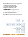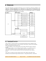
1
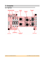
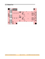
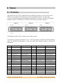
Form : QCF42
Date : 11 February 2009
Describes the demo and SMT911 operation.
SMT911
1.0
15 Jan. 10
C. H. Gray
Sundance Multiprocessor Technology Ltd, Chiltern House,
Waterside, Chesham, Bucks. HP5 1PS.
This document is the property of Sundance and may not be copied
nor communicated to a third party without prior written
permission.
© Sundance Multiprocessor Technology Limited 2009
SMT911 User Manual SMT911
Last Edited: 01/06/2010 10:09:00
1.0
Initial Release
SMT911 User Manual SMT911
15 Jan. 10
Page 2 of 38
CHG
Last Edited: 01/06/2010 10:09:00
1.1
Referenced Documents .............................................................................................. 7
2.1
Acronyms and Abbreviations ................................................................................... 8
3.1
Interface Description................................................................................................ 10
3.1.1 Electrical Description .......................................................................................... 10
3.2
Block Diagram............................................................................................................ 10
3.3
Module Description .................................................................................................. 11
3.3.1 Clock Distribution ................................................................................................ 11
3.3.2 JTAG........................................................................................................................ 11
3.3.3 Antenna Connectors ............................................................................................ 12
4.1
Functional Overview ................................................................................................. 13
4.2
Control Registers ...................................................................................................... 14
4.2.1 Control Packet Structure .................................................................................... 14
4.2.2 Reading and Writing Registers .......................................................................... 14
4.2.3 Register Map.......................................................................................................... 15
4.3
Running Demo ........................................................................................................... 16
4.3.1 Transmitter ........................................................................................................... 17
4.3.2 Receiver .................................................................................................................. 17
5.1
Top View ..................................................................................................................... 19
5.2
Bottom View ............................................................................................................... 20
6.1
SLB Interface .............................................................................................................. 21
10.1 2.4GHz Frequency Plan and Divider Ratio Programming Words .................... 25
10.2 5GHz Frequency Plan and Divider Ratio Programming Words ........................ 25
10.3 Reset Register 0x00 .................................................................................................. 26
SMT911 User Manual SMT911
Page 3 of 38
Last Edited: 01/06/2010 10:09:00
10.4 Test Register 0x01 .................................................................................................... 26
10.5 Function Register 0 – 0x02...................................................................................... 26
10.6 Function Register 1 – 0x03...................................................................................... 26
10.7 Function Register 2 – 0x04...................................................................................... 27
10.8 MAXIM A Register 0 – 0x05 (Standby)................................................................... 27
10.9 MAXIM A Register 1 – 0x06 (Integer-Divider Ration) ......................................... 28
10.10 MAXIM A Register 2 – 0x07 (Fractional-Divider Ratio) ...................................... 28
10.11 MAXIM A Register 3 – 0x08 (Band Select and PLL) ............................................. 28
10.12 MAXIM A Register 4 – 0x09 (Calibration) ............................................................. 29
10.13 MAXIM A Register 5 – 0x0A (Low-pass Filter) ..................................................... 29
10.14 MAXIM A Register 6 – 0x0B (RX Control/RSSI).................................................... 30
10.15 MAXIM A Register 7 – 0x0C (TX Linearity/Gain) ................................................. 30
10.16 MAXIM A Register 8 – 0x0D (RX Gain) .................................................................. 30
10.17 MAXIM A Register 9 – 0x0E (TX VGA Gain) .......................................................... 31
10.18 MAXIM B Register 0 – 0x0F (Standby) ................................................................... 31
10.19 MAXIM B Register 1 – 0x10 (Integer-Divider Ratio) ............................................ 31
10.20 MAXIM B Register 2 – 0x11 (Fractional-Divider Ratio) ....................................... 31
10.21 MAXIM B Register 3 – 0x12 (Band Select and PLL).............................................. 31
10.22 MAXIM B Register 4 – 0x13 (Calibration).............................................................. 31
10.23 MAXIM B Register 5 – 0x14 (Low-pass Filter) ...................................................... 31
10.24 MAXIM B Register 6 – 0x15 (RX Control/RSSI) .................................................... 31
10.25 MAXIM B Register 7 – 0x16 (TX Linearity/Gain) ................................................. 31
10.26 MAXIM B Register 8 – 0x17 (RX Gain) ................................................................... 31
10.27 MAXIM B Register 9 – 0x18 (TX VGA Gain) .......................................................... 32
10.28 ADDAC A Register 0 – 0x19 .................................................................................... 32
10.29 ADDAC A Register 1 – 0x1A ................................................................................... 32
10.30 ADDAC A Register 2 – 0x1B .................................................................................... 32
10.31 ADDAC A Register 3 – 0x1C ................................................................................... 33
10.32 ADDAC A Register 4 – 0x1D ................................................................................... 33
10.33 ADDAC A Register 5 – 0x1E .................................................................................... 33
10.34 ADDAC A Register 6 – 0x1F .................................................................................... 34
10.35 ADDAC A Register 7 – 0x20 .................................................................................... 34
10.36 ADDAC A Register 8 – 0x21 .................................................................................... 34
10.37 ADDAC A Register 9 – 0x22 .................................................................................... 35
10.38 ADDAC A Register 10 – 0x23 ................................................................................. 35
10.39 ADDAC A Register 11 – 0x24 ................................................................................. 36
10.40 ADDAC B Register 0 – 0x25 .................................................................................... 36
SMT911 User Manual SMT911
Page 4 of 38
Last Edited: 01/06/2010 10:09:00
10.41 ADDAC B Register 1 – 0x26 .................................................................................... 36
10.42 ADDAC B Register 2 – 0x27 .................................................................................... 36
10.43 ADDAC B Register 3 – 0x28 .................................................................................... 36
10.44 ADDAC B Register 4 – 0x29 .................................................................................... 36
10.45 ADDAC B Register 5 – 0x2A .................................................................................... 36
10.46 ADDAC B Register 6 – 0x2B .................................................................................... 36
10.47 ADDAC B Register 7 – 0x2C .................................................................................... 36
10.48 ADDAC B Register 8 – 0x2D.................................................................................... 36
10.49 ADDAC B Register 9 – 0x2E .................................................................................... 37
10.50 ADDAC B Register 10 – 0x2F .................................................................................. 37
10.51 ADDAC B Register 11 – 0x30 .................................................................................. 37
10.52 Update Register 0x31 ............................................................................................... 37
10.53 Update RSSI Register 0x32 ...................................................................................... 37
10.54 RSSI Register A 0x33 ................................................................................................ 37
10.55 RSSI Register B 0x34 ................................................................................................. 38
SMT911 User Manual SMT911
Page 5 of 38
Last Edited: 01/06/2010 10:09:00
The SMT911 is an advanced, high-quality MIMO transceiver card, designed to cover
all features of future high-speed MIMO radio systems. The SMT911 comprises two
complete, fully configurable transceiver chains between two dual 12-bit digital I/Q
interfaces and two dual-band 50 Ohm antenna ports for each channel.
Each transceiver chain is comprised of an integrated RF-frontend (band switch, T/R
switch and power amplifier), up-/down converters with on chip PLLs and high
performance analog-to-digital and digital-to-analog converters for the I/Q signals
and additional analog-to-digital converters for RSSI conversion.
With a single on-board crystal or externally supplied common reference clock for
the transceiver PLL‟s, multiple SMT911 cards are easily combined to build an
arbitrary size 2m x 2n MIMO system with coherent LO phase. All control signals,
data bits and the SPI bus are routed through a 120-pin QSH data connector
providing for flexible, application specific configuration and control during
operation. The SMT911 is designed to fit on and connect directly to an FPGA base
module like the Sundance SMT351T or SMT368. The provided demo SMT911
Firmware Control Module permits simple and unrestricted access to all control
registers from a user friendly C-Language API.
SMT911 User Manual SMT911
Page 6 of 38
Last Edited: 01/06/2010 10:09:00
SiGe Se2545A23: Dual Band 802.11 Wireless LAN Front End
MAX2828/2829: World-Class Transceiver-IC, MAXIM
AD9863: Analog Devices dual ADC/DAC
Sundance Local Bus: (SLB) specification
ftp2.sundance.com : TIM specification
SMT148FX: Carrier with 4 Module sites
SMT6048: Host-side USB software interface to Sundance hardware
SMT6002: Sundance Flash Programming Utility (FPGA)
SMT911 User Manual SMT911
Last Edited: 01/06/2010 10:09:00
A list of acronyms etc:
http://www.sundance.com/web/files/static.asp?pagename=acc
SMT911 User Manual SMT911
Last Edited: 01/06/2010 10:09:00
The SMT911 is an advanced, high-quality MIMO transceiver card, designed to cover
all features of future high-speed MIMO radio systems. It is used in combination with
Sundance base modules such as the SMT351T.
On the SMT911 transceiver card, two single-chip MIMO RF front-ends (SE2545A23)
are applied, containing nearly all circuitry required between the transceiver and the
antenna. Two transceiver chips of type MAXIM MAX2829 are used to up and downconvert signals between the WLAN carrier bands and the base-band. The MAX2829
is specially designed for MIMO/Smart Antenna application and the IEEE 802.11a/g
standard.
In order to fulfill the requirements of more simple and clever MIMO solutions, the
SMT911 transceiver card is equipped with two built-in ADC/DAC chips from Analog
Devices – AD9863. Each of the transceiver (MAXIM) chips is served by one AD9863.
The AD9863 integrates dual 12-bit ADCs and dual 12-bit DACs. The dual DACs
convert the digital base band I/Q signals to analog signals when the SMT911 card
acts as a transmitter. When the SMT911 card acts as receiver, the dual ADCs convert
the analog base-band I/Q signals into a digital format for the FPGA base board. Two
additional ADC‟s (AD7476) are provided to enable conversion of the Receive Signal
Strength Information (RSSI) from the MAXIM transceivers. All control pins of the
mentioned ICs above are routed through to the base module via the QSH connector. The
firmware on the base module offers the user flexibility to specify control signals and
control register settings. More details about the firmware are explained in the Firmware
implementation section.
The SMT911 card has two external reference clock inputs. These external clock inputs
provide the reference for generating the sampling clock in both ADC/DAC chips, and
provide the transceiver PLL‟s a reference for creating the required 2.4GHz or 5GHz
carrier frequency. Both of these circuits can be run for wider synchronization from
these connectors, or from a fixed, on-board oscillator output of 40MHz. The maximum
clocking speed of the internal ADC‟s is 50MHz, and the maximum clocking speed of the
internal DAC‟s is 200MHz (attainable through internal PLL multiplying).
SMT911 User Manual SMT911
Last Edited: 01/06/2010 10:09:00
• 4 SMA connectors (50 Ohm) for dual-band antennas providing TX/RX
• Two MMCX connectors (50 Ohm) external clock input
• Samtec BKT connector for 5 V and 3.3 V power supply
• 120-pin Samtec QSH connector for all digital I/O signals
• JTAG connector for debug/access to FPGA on base-board.
• Plugs directly into a wide range Sundance SLB TIMs
Each pin on the BKT power connector (33 pins in total) can carry 1.5 A. Digital 5V
(D+5V0), digital 3V3 (D+3V3) and digital ground (DGND) are provided over this
connector. D+3V3 and D+5V0 are assigned four pins each. The daughter card can
thus draw a total of 6A of each of these two supplies.
The major elements of the SMT911 are shown in the block diagram below (single
channel shown).
SMT911 User Manual SMT911
Page 10 of 38
Last Edited: 01/06/2010 10:09:00
There are two MMCX connector clock inputs for the SMT911. Clock A provides a
40MHz clock input for the MAXIM transceiver IC‟s. Clock B is the input for both
CLKIN1 and CLKIN 2 of ADC/DAC A and ADC/DAC B. Clock distribution is achieved
by two CDCV304 clock buffer drivers. Because the clock inputs to both pins CLKIN1
and CLKIN2 of the ADC/DAC‟s are shared, the clock provided here cannot exceed
50MHz (the maximum speed of the internal ADC‟s) if switching from TX to RX is the
ultimate goal. To achieve higher frequencies with the DAC‟s, the ADC/DAC‟s
internal PLL circuitry must be implemented to multiply and output the clock onto
IFACE2. This is programmable via SPI up to 200MHz.
For ease of use, a high quality 40MHz crystal has been placed on the mezzanine to
provide clocking for either both MAXIM transceivers, both ADC/DAC‟s, or all four
IC‟s. These configurations are selectable via jumpers 1 and 2.
Jumper
Both use XTAL
Both use External
XTAL CLKA/External CLKB
External CLKA/XTAL CLKB
CLKA
off
on
off
on
CLKB
off
on
on
off
The clock source is driven by two jumper controlled, multi-function gates that drive
two CDCV304 clock buffers. The jumper marked CLKA will select the source clock
for the MAXIM chip. With no jumper, the defaulted clock source is the onboard
40MHz crystal. With the jumper, the external CLK6 jack (J6) is then the chosen input
for the MAXIM clock. The same arrangement exists for CLKB, the clock source for
the ADDAC chips. If the jumper is attached, an external clock source (J3) is
expected; otherwise, the crystal will output a 40MHz clock to pins CLKIN1 and
CLKIN2 of the ADDAC chips.
The external clock jacks are AC coupled and so do not require any DC offset to
drive this logic. The clock provided to the MAXIM chip if external must be 40MHz
from a quality, stable source. The clock provided to the ADC/DAC chips must be a
quality, clean source and not exceed 50MHz if in a switching TX/RX configuration,
as this source clock feeds the internal ADC and DAC.
A standard Xilinx parallel JTAG header is supplied on the mezzanine to provide access
to the base modules JTAG chain.
SMT911 User Manual SMT911
Page 11 of 38
Last Edited: 01/06/2010 10:09:00
Four SMA antenna jacks are connected directly to the output of two SiGe RF frontend
IC‟s. Each channel shares both band A and band G on the same TX connector,
and both bands on the same RX connector. The antennas should be connected as
described below.
SMT911 User Manual SMT911
Page 12 of 38
Last Edited: 01/06/2010 10:09:00
The demo firmware provided will help you get started in using the SMT911 for
whatever custom applications are required. It is not meant to demonstrate the
hardware in its full capabilities, but to provide an example use for the device and an
example setup for configuration and control. It was developed using 3L‟s Diamond
development IDE for multiprocessor systems.
“SMT_control” is an NGC block for receiving instructions from a Sundance DSP
module, and passing on these control words to the SMT911 board. Some modules
which are integrated in this block are:
• Control Comport: receive instruction words, and send back register contents
to DSP.
• Switching Controller: run switching (TX, RX, Standby, etc.) of SMT911 board.
• SPI: send SPI signals to every corresponding chip on the SMT911 board.
• RSSI ADC: convert the RSSI and Power Detection information into register
words.
“SMT_data” is a block for data transfer between the ADDAC data pins and a
Sundance DSP module through an RSL interface. Using this RSL link, a sustained
SMT911 User Manual SMT911
Page 13 of 38
Last Edited: 01/06/2010 10:09:00
streaming speed of 250MB/s is possible, or burst transfers of 500MB/s (not taking
overhead into consideration). It also receives direct control words from the DSP
module, by getting the forwarded control worlds from the “SMT_control” module.
This block is supported by a DDR2 RAM interface available on the SMT351T board
for continuous playback in TX mode or as a buffer in RX mode.
These registers control the complete functionality of the SMT911 transceiver
mezzanine. They are set up via the Comport 3 of the base module.
The data passed to the FPGA over the Comports must conform to a certain packet
structure. Only after a valid packet is accepted and an update command sent will
the specified settings be applied. The packet structure is illustrated in the following
table.
Packet structure for writing (Byte 0 = 0x10)
Byte
0
1
2
3
Bit7
Bit6
Bit5
Bit4
Bit3
Bit2
Bit1
Bit0
“0”
Address7
Data15
Data7
“0”
Address6
Data14
Data6
“0”
Address5
Data13
Data5
“1”
Address4
Data12
Data4
“0”
Address3
Data11
Data3
“0”
Address2
Data10
Data2
“0”
Address1
Data9
Data1
“0”
Address0
Data8
Data0
Packet structure for reading (Byte 0 = 0x20)
Byte
0
1
2
3
Bit7
Bit6
Bit5
Bit4
Bit3
Bit2
Bit1
Bit0
“0”
Address7
Data15
Data7
“0”
Address6
Data14
Data6
“1”
Address5
Data13
Data5
“0”
Address4
Data12
Data4
“0”
Address3
Data11
Data3
“0”
Address2
Data10
Data2
“0”
Address1
Data9
Data1
“0”
Address0
Data8
Data0
Byte 0 of a packet must be 0x10 (for writing register) or 0x20 (for reading register).
This byte indicates the start of a packet and is required to synchronize
communication. Byte 1 denotes the register address to be accessed. Byte 2 is the
upper 8 bits of the data to the written or read, and Byte 3 is the lower 8 bits of the
data to be written or read, creating 16-bit data words.
Control packets are sent to the base module over Comport 3. This Comport is a 32-bit
bi-directional interface, so all four control bytes are written and read as one word.
SMT911 User Manual SMT911
Page 14 of 38
Last Edited: 01/06/2010 10:09:00
Greater detail on each register can be found in the Appendix.
Address
0x00
0x01
0x02
0x03
0x04
0x05
0x06
0x07
0x08
0x09
0x0A
0x0B
0x0C
0x0D
0x0E
0x0F
0x10
0x11
0x12
0x13
0x14
0x15
0x16
0x17
0x18
0x19
0x1A
Register Definition
Reset Register
Test Register
Function Register 0
Function Register 1
Function Register 2
MAXIM A Register 0
MAXIM A Register 1
MAXIM A Register 2
MAXIM A Register 3
MAXIM A Register 4
MAXIM A Register 5
MAXIM A Register 6
MAXIM A Register 7
MAXIM A Register 8
MAXIM A Register 9
MAXIM B Register 0
MAXIM B Register 1
MAXIM B Register 2
MAXIM B Register 3
MAXIM B Register 4
MAXIM B Register 5
MAXIM B Register 6
MAXIM B Register 7
MAXIM B Register 8
MAXIM B Register 9
ADDAC A Register 0
ADDAC A Register 1
SMT911 User Manual SMT911
Read/Write
W
R/W
R/W
R/W
R/W
R/W
R/W
R/W
R/W
R/W
R/W
R/W
R/W
R/W
R/W
R/W
R/W
R/W
R/W
R/W
R/W
R/W
R/W
R/W
R/W
R/W
R/W
Address
0x1B
0x1C
0x1D
0x1E
0x1F
0x20
0x21
0x22
0x23
0x24
0x25
0x26
0x27
0x28
0x29
0x2A
0x2B
0x2C
0x2D
0x2E
0x2E
0x30
0x31
0x32
0x33
0x34
Page 15 of 38
Register Definition
ADDAC A Register 2
ADDAC A Register 3
ADDAC A Register 4
ADDAC A Register 5
ADDAC A Register 6
ADDAC A Register 7
ADDAC A Register 8
ADDAC A Register 9
ADDAC A Register 10
ADDAC A Register 11
ADDAC B Register 0
ADDAC B Register 1
ADDAC B Register 2
ADDAC B Register 3
ADDAC B Register 4
ADDAC B Register 5
ADDAC B Register 6
ADDAC B Register 7
ADDAC B Register 8
ADDAC B Register 9
ADDAC B Register 10
ADDAC B Register 11
Update Register
Update RSSI Register
RSSI Channel A
RSSI Channel B
Read/Write
R/W
R/W
R/W
R/W
R/W
R/W
R/W
R/W
R/W
R/W
R/W
R/W
R/W
R/W
R/W
R/W
R/W
R/W
R/W
R/W
R/W
R/W
R=FW/W=SPI
W
R
R
Last Edited: 01/06/2010 10:09:00
Launching the demo application requires 3L‟s Diamond software suite to be
installed, at the very least the Server.
The demo is designed to be run using the SMT148-FX carrier board, with an SMT362
on TIM site 1 and an SMT351T-SX50 + SMT911 on TIM site 4. The comport
configuration for this SMT148-FX setup is the „default anti-clockwise‟. The latest
SMT6048 needs to be installed to connect to the SMT148-FX, and the SMT6002 will
be needed if the comport configuration of the carrier needs to be changed. If
„default clockwise‟ is instead loaded on the carrier, then the SMT351T-SX50 +
SMT911 can be alternately moved to TIM site 2, keeping the SMT362 in the same
position. (only T1C0 – T4C3 is used)
The „SMT911_Control.ngc‟ provides a ready to use interface for configuring the
registers of the mezzanine and switching between various states. This should not
need any modification when developing custom tasks, although new tasks or the
„Data‟ task can be modified any number of ways to create custom hardware
processing.
In the DSP task is an array called „BlockofRegisters[]‟ which has all the default
register configuration settings loaded at start-up. Details on the registers and the
structure for writing to specific fields can be found in the appendix. The datasheets
for the AD9863 and the MAXIM 2829 will offer further detailed information on what
each setting in these registers will do, and the format for writing to these registers
can be found in the header file for this task.
The applications depend on a couple folders being available, so these must be set
up first. On the „C‟ drive, make a new folder called „SMT911 Data‟, and in this folder
create a folder called „Received Data‟. The resulting path should be:
C:\SMT911 Data\Received Data\
Take the provided „SINE.dat‟ file and place it within the „SMT911 Data‟ folder. This is
the sample data file which the DSP will look for when loading the DDR memory for
transmit.
For both demo‟s, leave the jumpers off of the mezzanine to choose the onboard
crystal as the clock source, otherwise a larger system can be synchronized using an
external clock.
SMT911 User Manual SMT911
Page 16 of 38
Last Edited: 01/06/2010 10:09:00
The data file used when the module is configured as a transmitter must be
formatted so that each line provides a concatenated I/Q pair for the dual DAC‟s of
each channel. Each line will be read into the DSP and passed to the FPGA as straight
unsigned binary, with the first 12 bits corresponding to the „Q‟ value, and the next
12 bits corresponding to the „I‟ value. The following figure demonstrates this:
23
22
21
20
19
18
17
16
15
14
13
12
11
10
9
8
7
I
6
5
4
3
2
1
Q
To load the module as a transmitter, open a Diamond Server and launch
„SMT911_362_SX50T_TX.app‟. The application will begin by resetting the module for
correct initialization, then writing the default configuration settings to the registers
mapped in the FPGA. They are then double checked and written from the FPGA to
the mezzanine via SPI, at which time the module is placed in Standby and a menu is
presented. At this point, all four LED‟s on the SMT351T-SX50 should be on:
D3: MAXIM channel A good LO clock lock
D4: MAXIM channel B good LO clock lock
D5: DDR2 memory initialized successfully
D6: Good clock lock from both AD9863 IC‟s to the FPGA PLL
To step right through the demo using default settings, press „3‟ to load the
„SINE.dat‟ file into the DDR2 memory of the SMT351T-SX50, and then press „1‟ to
place the mezzanine into TX mode and repeatedly playback the stored memory
wave. The buffer that is created in the DSP‟s memory to store the data file needs to
be the same size as the number of samples in the data file. If a custom waveform is
to be selected for playback, this can be set at the top of the header file in the DSP
task by:
#define TxBUFSIZE
128
By default, the sine wave stored in memory will be played onto both channels A and
B of the mezzanine, but this can be altered in the „Data_TX.c‟ file in the DSP task.
To adjust the gain or to select a different carrier frequency, simply choose the
corresponding menu option and follow the directions as presented on screen. To
quit the application, press „9‟.
The receiver application works much the same way as the transmitter. Open a
Diamond Server and launch „SMT911_362_SX50T_RX.app‟. The mezzanine will reset
and initialize the mezzanine into Standby, then write all the configuration registers
in the FPGA with the default settings provided from „BlockofRegisters[]‟. These are
next double checked, and written via SPI to the ADC and transceiver IC‟s. At this
point a menu similar to the transmitter application should be presented, and all
four LED‟s on the SMT351T-SX50 should be on:
SMT911 User Manual SMT911
Page 17 of 38
Last Edited: 01/06/2010 10:09:00
0
D3: MAXIM channel A good LO clock lock
D4: MAXIM channel B good LO clock lock
D5: DDR2 memory initialized successfully
D6: Good clock lock from both AD9863 IC‟s to the FPGA PLL
To step through a simple capture from the module, press „1‟ to turn on the receiver.
Next press „5‟ to store a number of samples to the DDR2 memory of the FPGA base
module, and finally „6‟ to read the memory from the base module into a set of files
in „C:\SMT911 Data\Received Data\‟ called: „RxA_I.log‟, „RxA_Q.log‟, „RxB_I.log‟ and
„RxB_Q.log‟. The number of samples to be stored to file is changeable at the top of
the header file in the DSP task as:
#define DATALENGTH
(30*1024)
Keep in mind if more samples are attempted to be written to file than is stored in
memory, the server will halt and the application will need to be restarted.
The user is then free to analyze the data with their preferred application, or the
provided MATLAB script „Test_RX.m‟ can then be used to view the captured
waveforms.
To adjust the gain, monitor RSSI, or select a different carrier frequency, simply
choose the corresponding menu option and follow the directions as presented on
screen. To quit the application, press „9‟.
SMT911 User Manual SMT911
Page 18 of 38
Last Edited: 01/06/2010 10:09:00
SMT911 User Manual SMT911
Last Edited: 01/06/2010 10:09:00
SMT911 User Manual SMT911
Page 20 of 38
Last Edited: 01/06/2010 10:09:00
The SLB carries all LVTTL signals from the TIM base module to the devices on the
SMT911 mezzanine. The transceiver card is equipped with the 120-pin male
connector with the Samtec Part Number QSH-060-01-F-D-DP-A. The corresponding
female connector QTH-060-01-F-D-DP-A is located on the base module.
All signals routed by this connector are single-ended.
The pins are grouped in banks A, B, C, with the pin-out specified in the following
table. For further descriptions of the pins and their function, please consult the
datasheet.
Pin #
Pin Name
Signal Desc.
Pin #
Pin Name
Signal Desc.
1
ADQ_A_U<11>
Upper data pin 11
2
ADQ_A_U<10
Upper data pin 10
3
ADQ_A_U<9>
Upper data pin 9
4
ADQ_A_U<8>
Upper data pin 8
5
ADQ_A_U<7>
Upper data pin 7
6
ADQ_A_U<6>
Upper data pin 6
7
ADQ_A_U<5>
Upper data pin 5
8
ADQ_A_U<4>
Upper data pin 4
9
ADQ_A_U<3>
Upper data pin 3
10
ADQ_A_U<2>
Upper data pin 2
11
ADQ_A_U<1>
Upper data pin 1
12
ADQ_A_U<0>
Upper data pin 0
13
ADQ_A_L<11>
Lower data pin 11
14
ADQ_A_L<10>
Lower data pin 10
15
ADQ_A_L<9>
Lower data pin 9
16
ADQ_A_L<8>
Lower data pin 8
17
ADQ_A_L<7>
Lower data pin 7
18
ADQ_A_L<6>
Lower data pin 6
19
ADQ_A_L<5>
Lower data pin 5
20
ADQ_A_L<4>
Lower data pin 4
21
ADQ_A_L<3>
Lower data pin 3
22
ADQ_A_L<2>
Lower data pin 2
23
ADQ_A_L<1>
Lower data pin 1
24
ADQ_A_L<0>
Lower data pin 0
25
ADQ_A_SCLK
Serial clock ADQ A
26
ADQ_A_SDI
Serial DIN ADQ A
27
ADQ_A_CS
Serial CS ADQ A
28
ADQ_A_LOPWR
Low power ADQ A
29
ADQ_A_RXDWN
RXDWN ADQ A
30
ADQ_A_TXDWN
TXDWN ADQ A
31
ADQ_A_IFACE1
IFACE1 ADQ A
32
MAX_A_SER_CS
Serial CS Maxim A
33
ADQ_A_IFACE3
Clock ADQ A
34
MAX_A_TX_ENA
TX Enable Maxim A
SMT911 User Manual SMT911
Last Edited: 01/06/2010 10:09:00
35
ADQ_A_IFACE2
Cong. I/O ADQ A
36
MAX_A_SHDN
Shutdown Maxim A
37
MAX_A_SER_CLK
Serial clk Maxim A
38
MAX_A_RX_ENA
RX Enabel Maxim A
39
MAX_A_SER_DIN
Serial DIN Maxim A
40
MAX_A_RXHP
RXHP Maxim A
Pin #
Pin Name
Signal Desc.
Pin #
Pin Name
Signal Desc.
41
MAX_A_GAIN<0>
Gain B0 Maxim A
42
MAX_A_GAIN<1>
Gain B1 Maxim A
43
MAX_A_GAIN<2>
Gain B2 Maxim A
44
MAX_A_GAIN<3>
Gain B3 Maxim A
45
MAX_A_GAIN<4>
Gain B4 Maxim A
46
MAX_A_GAIN<5>
Gain B5 Maxim A
47
MAX_A_GAIN<6>
Gain B6 Maxim A
48
MAX_A_LD
Lock detect Maxim A
49
RESET_ADQAB
Reset ADQ A & B
50
RSSI_A_NCS
Serial CS RSSI ADC A
51
RSSI_A_SCLK
RSSI Maxim A
52
RSSI_A_SDATA
Serial DIN RSSI ADC A
53
SIGE1_TXRX
TXRX Select SiGe A
54
SIGE1_ENa
Band A PA SiGe A
55
SIGE1_ENg
Band G PA SiGe A
56
SIGE2_ENa
Band A PA SiGe B
57
SIGE2_ENg
Band G PA SiGe B
58
SIGE2_TXRX
TXRX Select SiGe B
59
RSSI_B_SDATA
Serial DIN RSSI ADC B
60
RSSI_B_SCLK
Serial clk RSSI ADC B
61
RSSI_B_NCS
Serial CS RSSI ADC B
62
MAX_B_LD
Lock detect Maxim B
63
MAX_B_GAIN<0>
Gain B0 Maxim B
64
MAX_B_GAIN<1>
Gain B1 Maxim B
65
MAX_B_GAIN<2>
Gain B2 Maxim B
66
MAX_B_GAIN<3>
Gain B3 Maxim B
67
MAX_B_GAIN<4>
Gain B4 Maxim B
68
MAX_B_GAIN<5>
Gain B5 Maxim B
69
MAX_B_GAIN<6>
Gain B6 Maxim B
70
Not Connected
71
Not Connected
72
Not Connected
73
Not Connected
74
Not Connected
75
Not Connected
76
Not Connected
77
Not Connected
78
Not Connected
79
Not Connected
80
Not Connected
Pin #
Pin Name
Signal Desc.
Pin #
Pin Name
Signal Desc.
81
ADQ_B_U<11>
Upper data pin 11
82
ADQ_B_U<10>
Upper data pin 10
83
ADQ_B_U<9>
Upper data pin 9
84
ADQ_B_U<8>
Upper data pin 8
85
ADQ_B_U<7>
Upper data pin n 7
86
ADQ_B_U<6>
Upper data pin 6
87
ADQ_B_U<5>
Upper data pin 5
88
ADQ_B_U<4>
Upper data pin 4
89
ADQ_B_U<3>
Upper data pin 3
90
ADQ_B_U<2>
Upper data pin 2
91
ADQ_B_U<1>
Upper data pin 1
92
ADQ_B_U<0>
Upper data pin 0
93
ADQ_B_L<11>
Lower data pin 11
94
ADQ_B_L<10>
Lower data pin 10
95
ADQ_B_L<9>
Lower data pin 9
96
ADQ_B_L<8>
Lower data pin 8
97
ADQ_B_L<7>
Lower data pin 7
98
ADQ_B_L<6>
Lower data pin 6
99
ADQ_B_L<5>
Lower data pin 5
100
ADQ_B_L<4>
Lower data pin 4
101
ADQ_B_L<3>
Lower data pin 3
102
ADQ_B_L<2>
Lower data pin 2
103
ADQ_B_L<1>
Lower data pin 1
104
ADQ_B_L<0>
Lower data pin 0
105
ADQ_B_SCLK
Serial clock ADQ B
106
ADQ_B_SDI
Serial DIN ADQ B
107
ADQ_B_CS
Serial enable ADQ B
108
ADQ_B_LOPWR
Low power ADQ B
SMT911 User Manual SMT911
Page 22 of 38
Last Edited: 01/06/2010 10:09:00
109
ADQ_B_IFACE1
IFACE1 ADQ B
110
ADQ_B_TXDWN
TXDWN ADQ B
111
ADQ_B_RXDWN
RXDWN ADQ B
112
MAX_B_SER_CS
Serial CS Maxim B
113
ADQ_B_IFACE3
Clock ADQ B
114
MAX_B_TX_ENA
TX enable Maxim B
115
ADQ_B_IFACE2
Conf. I/O ADQ B
116
MAX_B_SHDN
Shutdown Maxim B
117
MAX_B_SER_CLK
Serial clock Maxim B
118
MAX_B_RX_ENA
RX enable Maxim B
119
MAX_B_SER_DIN
Serial DIN Maxim B
120
MAX_B_RXHP
RXHP for Maxim B
SMT911 User Manual SMT911
Page 23 of 38
Last Edited: 01/06/2010 10:09:00
Dimensions
Weight
Supply Voltages
Supply Current
+12V
+5V
+3.3V
-5V
-12V
MTBF
This module presents no hazard to the user when in normal use.
This module is designed to operate from within an enclosed host system, which is
build to provide EMC shielding. Operation within the EU EMC guidelines is not
guaranteed unless it is installed within an adequate host system.
This module is protected from damage by fast voltage transients originating from
outside the host system which may be introduced through the output cables.
Short circuiting any output to ground does not cause the host PC system to lock up
or reboot.
SMT911 User Manual SMT911
Last Edited: 01/06/2010 10:09:00
fRF
(fRF x 4/3) /20MHz
Divider Ratio
Integer-Divider Ratio
Reg 0x06, B7-B0
Reg 0x07, B13-B0 (HEX)
Reg 0x06, B13-B12
2412
160.8000
1010 0000
3333
00
2417
161.1333
1010 0001
0888
10
2422
161.4667
1010 0001
1DDD
11
2427
161.8000
1010 0001
3333
00
2432
162.1333
1010 0010
0888
10
2437
162.4667
1010 0010
1DDD
11
2442
1628000
1010 0010
3333
00
2447
163.1333
1010 0011
0888
10
2452
163.4667
1010 0011
1DDD
11
2457
163.8000
1010 0011
3333
00
2462
164.1333
1010 0100
0888
10
2467
164.4667
1010 0100
1DDD
11
2472
164.8000
1010 0100
3333
00
2484
165.6000
1010 0101
2666
01
fRF
(fRF x 4/3) /20MHz
Divider Ratio
Integer-Divider Ratio
Reg 0x06, B7-B0
Reg 0x07, B13-B0 (HEX)
Reg 0x06, B13-B12
5180
207.2
1100 1111
0CCC
11
5200
208.0
1101 0000
0000
00
5220
208.8
1101 0000
3333
00
5240
209.6
1101 0001
2666
01
5260
210.4
1101 0010
1999
10
5280
211.2
1101 0011
0CCC
11
5300
2122.0
1101 0100
0000
00
5320
212.8
1101 0100
3333
00
5500
220.0
1101 1100
0000
00
5520
220.8
1101 1100
3333
00
5540
221.6
1101 1101
2666
01
5560
222.4
1101 1110
1999
10
5580
223.2
1101 1111
0CCC
11
5600
224.0
1110 0000
0000
00
5620
224.8
1110 0000
3333
00
5640
225.6
1110 0001
2666
01
5660
226.4
1110 0010
1999
10
5680
227.2
1110 0011
0CCC
11
5700
228.0
1110 0100
0000
00
5745
229.8
1110 0101
3333
00
5765
230.6
1110 0110
2666
01
5785
231.4
1110 0111
1999
10
MHZ
MHZ
SMT911 User Manual SMT911
Fractional-Divider Ratio
Fractional-Divider Ratio
Page 25 of 38
Last Edited: 01/06/2010 10:09:00
5805
232.2
1110 1000
0CCC
11
This register resets some of the components. In order to save on power, the
components will remain in reset until the register is cleared.
Byte 1-0
Default
D15
0
D14
0
D13
0
D12
0
D11
0
D10
0
D9
0
D8
0
D7
0
D6
0
D5
0
D4
0
D3
0
D2
0
D1
1
D0
1
D1
1
D0
0
Reconfigurable bits:
Bit
1
0
Default
0
0
Description
ADQ A & B reset, „1‟ = reset, „0‟ = normal operation
Transceiver A & B Reset ; “1”= reset, “0” = normal operation
Any 16-bit word can be written and read from this register to verify proper
operation of the Comport.
Byte 1-0
Default
D15
1
D14
1
D13
1
D12
1
D11
0
D10
0
D9
0
D8
0
D7
1
D6
0
D5
1
D4
0
D3
1
D2
0
This register allows the basic setup of the SMT911 transceiver card; including
activating MIMO operation, choosing the frequency band, selecting memory, and
defining TX or RX operation.
Byte 1-0
Default
D15
0
D14
0
D13
0
D12
0
D11
0
D10
0
D9
0
D8
0
D7
0
D6
0
D5
0
D4
0
D3
0
D2
0
D1
1
D0
1
Reconfigurable bits:
Bit
3
2
1
0
Default
0
0
1
1
Description
“0” =use memory (DDR2 RAM) , “1” = no memory (direct transfer)
Working mode. “1” = Receiver, “0” = Transmitter
Frequency range. “0” = 2.4 GHz (802.11g), “1” = 5.2 GHz (802.11a)
MIMO activation. „0‟ = SISO mode (only path A) „1‟ = MIMO active.
This register controls the switching of the SMT911; either active (TX/RX) or standby
Byte 1-0
Default
D15
0
D14
0
D13
0
D12
0
D11
0
D10
0
D9
0
D8
0
D7
0
D6
0
D5
0
D4
0
D3
0
D2
0
D1
0
D0
0
Reconfigurable bits:
SMT911 User Manual SMT911
Page 26 of 38
Last Edited: 01/06/2010 10:09:00
Bit
7
6
5
4
3
2
1
0
Default
0
0
0
0
0
0
0
0
Description
„1‟ = write to memory, „0‟ = stop write to memory
„1‟ = read from memory, „0‟ = don‟t read from memory
“000000” = standby
“111111” = active (actual working mode depends on register 0x02
By default, the gain control is applied through the parallel digital inputs of the
MAXIM chips. This register is used to set these digital inputs.
Byte 1-0
Default
D15
0
D14
0
D13
0
D12
0
D11
0
D10
0
D9
0
D8
0
D7
0
D6
0
D5
0
D4
0
D3
0
D2
0
D1
0
D0
0
Reconfigurable bits:
Bit
13
12
11
10
9
8
7
6
5
4
3
2
1
0
Default
0
0
0
0
0
0
0
0
0
0
0
0
0
0
Description
Bit 13:Bit 7 are digital gain control of MAXIM B
As Receiver:
B13:B12 are used for Rx LNA gain control. 00”&“01” = minimum, “10” = medium, “11” = maximum.
B11:B7 are used for Rx VGA gain control. “00000” = 0 dB (minimum), “11111” = 62 dB (maximum).
As Transmitter
B13 is not used, B12:B7 is used for Tx VGA gain control. “000000” = 0 dB (minimum), “111111” =
30 dB (maximum)
Bit6:Bit0, are digital gain control for MAXIM A.
As Receiver:
B6:B5 are used for Rx LNA gain control. “00”&“01” = minimum, “10” = medium, “11” = maximum.
B4:B0 are used for Rx VGA gain control. “00000” = 0 dB (minimum), “11111” = 62 dB (maximum).
As Transmitter:
B6 is not used, B5:B0 is used for Tx VGA gain control. “000000” = 0 dB (minimum), “111111” = 30
dB (maximum)
Various internal blocks of the MAXIM chip can be turned on or off by setting this
standby register. Setting bit 13 to 1 turns the clock on, while setting it to 0 turns the
block off.
Byte 1-0
Default
D15
0
D14
0
D13
0
D12
1
D11
0
D10
0
D9
0
D8
0
D7
0
D6
0
D5
0
D4
0
D3
0
D2
1
D1
1
D0
1
Reconfigurable bits:
Bit
13
11
10
Default
1
0
0
Description
MIMO mode: „0‟ = normal operation, „1‟ = MIMO applications
Voltage Reference
PA Bias DAC, in TX Mode
SMT911 User Manual SMT911
Page 27 of 38
Last Edited: 01/06/2010 10:09:00
This register contains the integer portion of the divider ratio of the synthesizer.
This register in conjunction with the fractional-divider ratio register, permits
selection of a precise frequency. Please refer to the appendix tables.
Byte 1-0
Default
D15
0
D14
0
D13
1
D12
1
D11
0
D10
0
D9
0
D8
0
D7
1
D6
0
D5
1
D4
0
D3
0
D2
0
D1
1
D0
1
Reconfigurable bits:
Bit
13
12
7
6
5
4
3
2
1
0
Default
1
1
1
0
1
0
0
0
1
0
Description
2 LSBs of the Fractional-Divider Ratio
Integer-Divider Ratio Word Programming Bits. Valid values are from
128(Bit7:Bit0 = “10000000”) to 255 (Bit7:Bit0 = “11111111”)
This register (along with bit 13 and bit 12 of the integer divider ratio register)
controls the fractional-divider ratio with 16-bit resolution. Bit 13 to bit 0 of this
register combined with bit 13 and bit 12 of the integer-divider ratio register form
the whole fractional-divider ratio. To retain the complete frequency plan please
refer to the appendix tables.
Byte 1-0
Default
D15
0
D14
0
D13
0
D12
1
D11
1
D10
1
D9
0
D8
1
D7
1
D6
1
D5
0
D4
1
D3
1
D2
1
D1
0
D0
1
Reconfigurable bits:
Bit
13
12
11
10
9
8
7
6
5
4
3
2
1
0
Default
0
1
1
1
1
1
1
1
0
1
1
1
0
1
Description
Bit0:Bit13 = refer to Appendix : Frequency Plan and Divider Ratio Programming Words
This register configures the programmable-reference frequency dividers for the
SMT911 User Manual SMT911
Page 28 of 38
Last Edited: 01/06/2010 10:09:00
synthesizer, and sets the DC current for the charge pump. The programmable
reference frequency divider provides the reference frequency to the phase detector
by dividing the signal of the crystal oscillator.
Byte 1-0
Default
D15
0
D14
0
D13
1
D12
1
D11
1
D10
0
D9
0
D8
0
D7
0
D6
0
D5
1
D4
0
D3
0
D2
1
D1
0
D0
0
Reconfigurable bits:
Bit
13
10
9
8
Default
0
0
0
0
7
6
0
0
5
3
2
1
0
0
0
0
0
0
Description
„0‟ = normal operation, „1‟ = MIMO applications
These Bits set the VCO Sub-Band when programmed by using SPI (Bit8=1).
“00” = lowest frequency band; “11” = highest frequency band.
VCO SPI Bandswitch Enable. “0” = disable SPI control, bandswitch is done by
FSM; “1” = bandswitch is done by SPI programming.
VCO Bandswitch Enable. “0” = disable; “1” = start automatic bandswitch.
RF Frequency Band Select in 802.11a Mode (Bit0=1). “0” = 4.9GHz to 5.35GHz band; “1” = 5.47GHz
to 5.875GHz Band.
PLL Charge-Pump-Current Select. “0” = 2mA, “1” = 4mA.
These Bits Set the Reference-Divider Ratio. “001” corresponds to R = 1 and “111” corresponds to R
= 7.
RF Frequency Band Select. “0” = 2.4GHz Band; “1” = 5GHz band.
This register configures the TX/RX calibration modes.
Byte 1-0
Default
D15
0
D14
0
D13
0
D12
1
D11
1
D10
1
D9
0
D8
0
D7
0
D6
0
D5
0
D4
0
D3
0
D2
0
D1
0
D0
0
D1
1
D0
0
Reconfigurable bits:
Bit
12
11
1
0
Default
1
1
0
0
Description
Transmitter I/Q Calibration LO Leakage and Sideband-Detector Gain-Control Bits.
“00” = 8 dB; “01” = 18 dB; “10” = 24 dB; “11” = 34 dB
“0” = TX Calibration Mode Disabled; “1” = TX Calibration Mode Enabled
“0” = RX Calibration Mode Disabled; “1” = RX Calibration Mode Enabled
This register allows the adjustment of the RX and TX low-pass filter corner
frequencies
Byte 1-0
Default
D15
0
D14
0
D13
0
D12
0
D11
0
D10
0
D9
0
D8
0
D7
0
D6
0
D5
1
D4
0
D3
1
D2
0
Reconfigurable bits:
Bit
11
6
5
4
3
2
1
0
Default
0
0
0
0
0
0
0
0
Description
RSSI High Bandwidth Enable. “0” = 2 MHz; “1” = 6MHz
TX LPF Corner Frequency Coarse Adjustment. “00” = undefined; “01” = 12MHz (nominal
mode); “10” = 18MHz (turbo mode 1); “11” = 24MHz (turbo mode 2).
RX LPF Corner Frequency Coarse Adjustment. “00” = 7.5MHz; “01” = 9.5MHz (nominal
mode); “10” = 14 MHz (turbo mode 1); “11” = 18MHz (turbo mode 2).
RX LPF Corner Frequency Fine Adjustment (Relative to the Course Setting).
“000” = 90%; “001” = 95%; “010” = 100%; “011” = 105%; “100” =110%.
SMT911 User Manual SMT911
Page 29 of 38
Last Edited: 01/06/2010 10:09:00
This register is used to adjust the RX section and RSSI output.
Byte 1-0
Default
D15
0
D14
0
D13
0
D12
0
D11
0
D10
0
D9
0
D8
0
D7
0
D6
0
D5
1
D4
0
D3
0
D2
1
D1
0
D0
1
D1
0
D0
0
Reconfigurable bits:
Bit
12
Default
0
11
10
0
0
8
0
2
1
Description
Enable Rx VGA Gain Programming Serially. “0” = Rx VGA gain programmed with
external digital inputs (B7:B1); “1” = Rx VGA gain programmed with serial data bits in the
Rx gain register (D6:D0).
RSSI Output Range. “0” = low range (0.5V to 2V); “1” = high range (0.5V to 2.5V).
RSSI Operating Mode. “0” = RSSI disabled if RXHP = 0, and enabled if RXHP = 1;
“1” = RSSI enabled independent of RXHP
RSSI Pin Function. “0” = outputs RSSI signal in Rx mode; “1” = outputs temperature
sensor voltage in Rx, Tx and standby modes.
Rx high-pass -3dB Corner Frequency when RXHP = 0. “0” = 100Hz; “1” = 30kHz
This register allows the adjustment of the TX gain and linearity
Byte 1-0
Default
D15
0
D14
0
D13
0
D12
0
D11
0
D10
0
D9
1
D8
0
D7
0
D6
0
D5
0
D4
0
D3
0
D2
0
Reconfigurable bits:
Bit
10
Default
0
9
8
7
6
3
2
1
0
1
0
0
0
0
0
0
0
Description
Enable Tx VGA Gain Programming Serially. “0” = Tx VGA gain programmed with external
digital inputs (B6:B1); “1” = Tx VGA gain programmed with data bits in the Tx gain
register (D5:D0).
PA Driver linearity. “00” = 50% current (minimum linearity); “01” = 63% current;
“10” = 78% current; “11” = 100% current (maximum linearity)
Tx VGA linearity. “00” = 50% current (minimum linearity); “01” = 63% current;
“10” = 78% current; “11” = 100% current (maximum linearity)
Tx Upconverter Linearity. “00” = 50% current (minimum linearity); “01” = 63% current;
“10” = 78% current; “11” = 100% current (maximum linearity).
Tx Base-band Gain. “00” = max base-band gain -5dB; “01” = max base-band gain -3dB;
“10” = max base-band gain -1.5dB; “11” = max base-band gain.
This register sets the RX base-band gain and RF gain when MAXIM A Register 6 Bit12
= „1‟.
Byte 1-0
Default
D15
0
D14
0
D13
0
D12
0
D11
0
D10
0
D9
0
D8
0
D7
0
D6
1
D5
1
D4
1
D3
1
D2
1
D1
1
D0
1
Reconfigurable bits:
Bit
6
5
4
Default
1
1
1
Description
Rx base-band and RF gain-control bits. Bit 6 maps to digital input pin B1. Bit6:BitD0 = “0000000”
corresponds to minimum gain.
SMT911 User Manual SMT911
Page 30 of 38
Last Edited: 01/06/2010 10:09:00
3
2
1
0
1
1
1
1
This register sets the TX VGA gain when MAXIM A Register 7 Bit10 = „1‟.
Byte 1-0
Default
D15
0
D14
0
D13
0
D12
0
D11
0
D10
0
D9
0
D8
0
D7
0
D6
0
D5
0
D4
0
D3
0
D2
0
D1
0
D0
0
Reconfigurable bits:
Bit
5
4
3
2
1
0
Default
0
0
0
0
0
0
Description
For faster Tx VGA gain setting, only Bit5:Bit0 need to be programmed.
Tx VGA Gain Control. Bit5 maps to digital input pin B6 and Bit0 maps to digital input pin
B1. Bit5:Bit0 = “000000” corresponds to minimum gain.
Same settings as MAXIM A. See corresponding register.
Same settings as MAXIM A. See corresponding register.
Same settings as MAXIM A. See corresponding register.
Same settings as MAXIM A. See corresponding register.
Same settings as MAXIM A. See corresponding register.
Same settings as MAXIM A. See corresponding register.
Same settings as MAXIM A. See corresponding register.
Same settings as MAXIM A. See corresponding register.
Same settings as MAXIM A. See corresponding register.
SMT911 User Manual SMT911
Page 31 of 38
Last Edited: 01/06/2010 10:09:00
Same settings as MAXIM A. See corresponding register.
This register is used for general setting and clock mode of ADDAC A.
Byte 1-0
Default
D15
0
D14
0
D13
0
D12
0
D11
0
D10
0
D9
0
D8
0
D7
1
D6
0
D5
0
D4
0
D3
0
D2
0
D1
0
D0
0
Reconfigurable bits:
Bit
15
14
13
10
9
7
6
5
Default
0
0
0
0
0
0
0
0
Description
Clock Mode setting. “000” standard FD, HD10, HD20 (modes 1,4,7); “001” Optional FD
timing (mode 2) ; “010” not used; “011” Optional HD20 timing (mode 5); “100” not used;
“101” Optional HD10 timing (mode 8); “110” not used; “111” Clone Mode (mode 10)
Enable the IFACE2 port to be an output clock
Inv the output clock on IFACE3
SDIO pin. “0” = uni-directional ; “1” = bidirectional
SPI Mode. “0” = MSB; “1” = LSB
Soft Reset. “0” = not reset; “1” = reset register to default value
This register is used to set Power-Down mode of ADDAC A.
Byte 1-0
Default
D15
0
D14
0
D13
0
D12
0
D11
0
D10
0
D9
0
D8
0
D7
0
D6
0
D5
0
D4
0
D3
0
D2
0
D1
0
D0
0
D4
0
D3
0
D2
0
D1
0
D0
0
Reconfigurable bits:
Bit
15
14
7
6
5
4
3
2
1
Default
0
0
0
0
0
0
0
0
0
Description
Rx_A Analog Power-Down. “0” = active; “1” = Power-down
Rx_A DC Bias Analog Power-Down. “0” = active; “1” = Power-down
Power Down Tx Analog. “000” = default; “100 = Power down Tx A;
“010” = Power-Down Tx B; “111 = Power-Down Tx A and Tx B
Tx Digital Power-Down. “0” = active; “1” = Power-down
Rx Digital Power-Down. “0” = active; “1” = Power-down
PLL Power-Down. “0” = active; “1” = Power-down
PLL Output Disconnect. “0” = connect; “1” = disconnect
This register is used to set Power-Down of ADDAC A.
Byte 1-0
Default
D15
0
D14
0
D13
0
D12
0
D11
0
D10
0
D9
0
D8
0
D7
0
D6
0
D5
0
Reconfigurable bits:
Bit
Default
Description
SMT911 User Manual SMT911
Page 32 of 38
Last Edited: 01/06/2010 10:09:00
15
14
13
12
7
6
0
0
0
0
0
0
Rx Analog Bias Power-Down. “0” = active; “1” = Power-Down
RxRef Power-Down. “0” = active; “1” = Power-Down
DiffRef Power-Down. “0” = active; “1” = Power-Down
VREF Power-Down. “0” = active; “1” = Power-Down
Rx_B Analog Power-Down. “0” = active; “1” = Power-down
Rx_B DC Bias Power-Down. “0” = active; “1” = Power-down
This register is used to set Rx Path of ADDAC A.
Byte 1-0
Default
D15
0
D14
0
D13
0
D12
0
D11
0
D10
0
D9
0
D8
0
D7
0
D6
0
D5
0
D4
0
D3
0
D2
0
D1
0
D0
0
Reconfigurable bits:
Bit
13
12
5
4
Default
0
0
0
0
Description
Rx_B 2‟s complement. “0” = straight binary; “1” = 2‟s complement
Rx_B Clk Duty. “0” = disable; “1” = enable
Rx_A 2‟s complement. “0” = straight binary; “1” = 2‟s complement
Rx_A Clk Duty. “0” = disable; “1” = enable
This register is used to set Ultra low power control of Rx path of ADDAC A, in
combination with asserting the ADC_LO_PWR pin to reduce power consumption.
Byte 1-0
Default
D15
0
D14
0
D13
0
D12
0
D11
0
D10
0
D9
0
D8
0
D7
0
D6
0
D5
0
D4
0
D3
0
D2
0
D1
0
D0
0
Reconfigurable bits:
Bit
14
13
12
3
2
Default
0
0
0
0
0
Description
Rx Ultralow
Rx Ultralow
Rx Ultralow
Rx Ultralow
Rx Ultralow
PowerControl.
PowerControl.
PowerControl.
PowerControl.
PowerControl.
“0”
“0”
“0”
“0”
“0”
=
=
=
=
=
normal;
normal;
normal;
normal;
normal;
“1”
“1”
“1”
“1”
“1”
=
=
=
=
=
set to Ultralow
set to Ultralow
set to Ultralow
set to Ultralow
set to Ultralow
This register is used to set Ultra low power control of Rx path and DAC A Offset of
ADDAC A.
Byte 1-0
Default
D15
0
D14
0
D13
0
D12
0
D11
0
D10
0
D9
0
D8
0
D7
0
D6
0
D5
0
D4
0
D3
0
D2
0
D1
0
D0
0
Reconfigurable bits:
Bit
15
14
13
12
11
Default
0
0
0
0
0
Description
DAC A Offset [9:2]
SMT911 User Manual SMT911
Page 33 of 38
Last Edited: 01/06/2010 10:09:00
10
9
8
6
5
4
0
0
0
0
0
0
Rx Ultralow PowerControl. “0” = normal; “1” = set to Ultralow
Rx Ultralow PowerControl. “0” = normal; “1” = set to Ultralow
Rx Ultralow PowerControl. “0” = normal; “1” = set to Ultralow
This register is used for DAC A offset and DAC A gain control of ADDAC A.
Byte 1-0
Default
D15
0
D14
0
D13
0
D12
0
D11
0
D10
0
D9
0
D8
0
D7
0
D6
0
D5
0
D4
0
D3
0
D2
0
D1
0
D0
0
D1
0
D0
0
Reconfigurable bits:
Bit
15
14
13
12
11
10
9
8
7
6
0
Default
0
0
0
0
0
0
0
0
0
0
0
Description
DAC A Coarse Gain Control. “00” = output current scaling by 1/11; “01” = output current
scaling by ½; “10” and “11” = no output current scaling
DAC A Fine Gain [5:0] := “100000” Maximum positive gain adjustment;
“111111” Minimum positive gain adjustment;
“000000” default of no adjustment;
“000001” Minimum negative gain adjustment;
“011111” Maximum negative gain adjustment
DAC A Offset [1:0]
DAC A Offset Direction. “0” = to negative diff. pin; “1” = to positive diff. pin
This register is used for DAC B offset and its direction of ADDAC A.
Byte 1-0
Default
D15
0
D14
0
D13
0
D12
0
D11
0
D10
0
D9
0
D8
0
D7
0
D6
0
D5
0
D4
0
D3
0
D2
0
Reconfigurable bits:
Bit
15
14
8
7
6
5
4
3
2
1
0
Default
0
0
0
0
0
0
0
0
0
0
0
Description
DAC B Offset [1:0]
DAC B Offset Direction. “0” = to negative diff. pin; “1” = to positive diff. pin
DAC B Offset [9:2]
This register is used for DAC B offset gain control, fine gain, and TxPGA gain of
ADDAC A.
Byte 1-0
D15
D14
D13
D12
SMT911 User Manual SMT911
D11
D10
D9
D8
Page 34 of 38
D7
D6
D5
D4
D3
D2
D1
D0
Last Edited: 01/06/2010 10:09:00
Default
1
1
1
1
1
1
1
1
0
0
0
0
0
0
0
0
Reconfigurable bits:
Bit
15
14
13
12
11
10
9
8
7
6
5
4
3
2
1
0
Default
1
1
1
1
1
1
1
1
0
0
0
0
0
0
0
0
Description
TxPGA Gain [7:0], is register control for the Tx programmable gain amplifier (TxPGA).
The TxPGA provides a 20 dB continuous gain range with 0.1 dB steps (linear in dB)
simultaneously to both Tx channels. Default is 0xFF.
“0000 0000” = Minimum gain scaling -20 dB
“1111 1111” = Maximum gain scaling 0dB
DAC B Coarse Gain Control. “00” = output current scaling by 1/11; “01” = output current
scaling by ½; “10” and “11” no output current scaling
DAC B Fine Gain [5:0] := “100000” Maximum positive gain adjustment;
“111111” Minimum positive gain adjustment;
“000000” default of no adjustment;
“000001” Minimum negative gain adjustment;
“011111” Maximum negative gain adjustment
This register is used for other settings of Tx Path and I/O configuration of ADDAC
A.
Byte 1-0
Default
D15
0
D14
0
D13
0
D12
0
D11
0
D10
0
D9
0
D8
0
D7
0
D6
0
D5
0
D4
0
D3
0
D2
0
D1
0
D0
0
Reconfigurable bits:
Bit
15
14
13
9
8
6
Default
0
0
0
0
0
0
4
0
Description
Tx Twos Complement. “0” = straight binary; “1” = twos complement
Rx Twos Complement. “0” = straight binary; “1” = twos complement
Tx Inverse Sample. “0” = sampled on rising edge; “1” = sampled on falling edge clock
Interpolation control.
“00” = filters bypassed; “01” = interpolation rate 2x; “10” = interpolation rate 4x.
TxPGA Slave Enable. “0” = immediately after register updated; “1” = synchronized with
falling edge of a signal applied to the TxPwrDwn
TxPGA Fast Update. “0” = normal mode; “1” = fast mode
This register is used for I/O configuration and clock configuration of ADDAC A.
Byte 1-0
Default
D15
0
D14
0
D13
0
D12
0
D11
0
D10
0
D9
0
D8
0
D7
0
D6
0
D5
0
D4
0
D3
0
D2
0
D1
0
D0
0
Reconfigurable bits:
Bit
15
13
12
11
10
9
8
Default
0
0
0
0
0
0
0
Description
PLL Bypass. “0” = PLL remains active; “1” = PLL bypassed
ADC Clock Div. “0” = no division; “1” = divides the clock by 2
Alt timing mode. “0” = normal timing operation; “1” = alternative operation mode
PLL Div5. “0” = no division; “1” = output of PLL divided by 5
PLL multiplication factor.
“000” = 1x; “001” = 2x; “010” = 4x; “011” = 8x; “100” = 16x; “101” ~ “111”: not used.
SMT911 User Manual SMT911
Page 35 of 38
Last Edited: 01/06/2010 10:09:00
5
4
3
2
1
0
0
0
0
0
0
0
Dig Loop On. “0” = off; “1” = on (on only in full duplex mode)
SpiFDnHD. “0” = HD mode; “1” = FD mode
SpiTxnRx for toggling Tx & Rx in HD mode. “0” = Rx; “1” = Tx
SpiB10n20, option for 10 or 20 bit. “0” = 20-bit; “1” = 10-bit
SPI IO Control, in conjunction with Bit3 to override external TxnRx pin operation
SpiClone. “1” = for clone mode; “0” = other
This register is used for configuring the rest of the clock settings of ADDAC A.
Byte 1-0
Default
D15
0
D14
0
D13
0
D12
0
D11
0
D10
0
D9
0
D8
0
D7
0
D6
0
D5
0
D4
0
D3
0
D2
0
D1
0
D0
0
Reconfigurable bits:
Bit
5
2
Default
0
0
Description
PLL to IFACE2. “0” = IFACE2 normal; “1” = IFACE2 switched to PLL output clock (FD)
PLL Slow. “0” = standard; “1” = changes phase noise generated from the PLL clock
Same settings as ADDAC A. See corresponding register.
Same settings as ADDAC A. See corresponding register.
Same settings as ADDAC A. See corresponding register.
Same settings as ADDAC A. See corresponding register.
Same settings as ADDAC A. See corresponding register.
Same settings as ADDAC A. See corresponding register.
Same settings as ADDAC A. See corresponding register.
Same settings as ADDAC A. See corresponding register.
Same settings as ADDAC A. See corresponding register.
SMT911 User Manual SMT911
Page 36 of 38
Last Edited: 01/06/2010 10:09:00
Same settings as ADDAC A. See corresponding register.
Same settings as ADDAC A. See corresponding register.
Same settings as ADDAC A. See corresponding register.
The Update bit activates the serial interface (SPI) to pass registers previously written
in the FPGA to the corresponding device (MAXIM A and B, and ADDAC A and B).
Byte 1-0
Default
D15
0
D14
0
D13
0
D12
0
D11
0
D10
0
D9
0
D8
0
D7
0
D6
0
D5
0
D4
0
D3
1
D2
1
D1
1
D0
1
D5
D4
D3
D2
Firmware Version
D1
D0
D5
0
Reading back this register returns the Firmware version.
Byte 1-0
Default
D15
0
D14
0
D13
0
D12
0
D11
0
D10
0
D9
0
D8
0
D7
D6
Reconfigurable bits:
Bit
3
2
1
0
Default
1
1
1
1
Description
ADDAC B Update. “0” = not updated; “1” = updated
ADDAC A Update. “0” = not updated; “1” = updated
MAXIM B Update. “0” = not updated; “1” = updated
MAXIM A Update. “0” = not updated; “1” = updated
This register is used to update the detected RSSI values.
Byte 1-0
Default
D15
0
D14
0
D13
0
D12
0
D11
0
D10
0
D9
0
D8
0
D7
0
D6
0
D4
0
D3
1
D2
1
D1
1
D0
1
D4
D3
D2
D1
D0
Reconfigurable bits:
Bit
1
0
Default
0
0
Description
“0” = not updated, “1” = update RSSI / Power Detect of Channel B
“0” = not updated, “1” = update RSSI / Power Detect of Channel A
This read only register retrieves the RSSI value from channel A.
Byte 1-0
Default
D15
0
D14
0
D13
0
D12
0
SMT911 User Manual SMT911
D11
D10
D9
D8
Page 37 of 38
D7
D6
D5
A[11:0]
Last Edited: 01/06/2010 10:09:00
This read only register retrieves the RSSI value from channel B.
Byte 1-0
Default
D15
0
D14
0
D13
0
D12
0
SMT911 User Manual SMT911
D11
D10
D9
D8
Page 38 of 38
D7
D6
D5
B[11:0]
D4
D3
D2
D1
D0
Last Edited: 01/06/2010 10:09:00