1
unsigned or signed counter. On the Kinetis K60 there are three instances of FTM. One FTM has
8 channels, the other two FTMs have 2 channels.
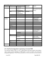
The procedure to configure the FlexTimer for generating a center-aligned PWM with dead time
insertion is described in the application note AN3729 [6].
Because the referenced application note supports an earlier version (1.0) of the FlexTimer
implemented on the ColdFire V1, and with respect to the hardware used (TWR-MC-LV3PH),
there are a few differences in the configuration, as described below:
•
•
•
•
•
•
•
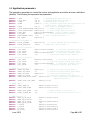
Initially, it is necessary to enable the system clock for the FlexTimer module in the Clock
Gating Control Register:
SIM_SCGC6 |= SIM_SCGC6_FTM0_MASK;
It is necessary to disable the write protection of some registers before they can be
updated:
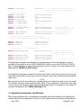
FTM0_MODE |= FTM_MODE_WPDIS_MASK;
It is advisable to enable the internal FlexTimer counter to run in debug mode:
FTM0_CONF |= FTM_CONF_BDMMODE(3);
While the HW debugging interface (jLink, Multilink…) is connected to the microcontroller,
the MCU is in debug mode. This does not depend on whether the running code
containing breakpoints or not.
The PWM signals generated by the FlexTimer0 are directly connected to the MOSFET
driver. Due to safety reasons, the input signals for the top transistors on the MOSFET
driver used on the Tower low-voltage power stage have inversed polarity. Therefore, it is
also necessary to set the right polarity of the PWM signals:
FTM0_POL = FTM_POL_POL0_MASK |
FTM_POL_POL2_MASK |
FTM_POL_POL4_MASK;
The duty cycle is changed by changing the value of the FlexTimer Value registers. These
registers are double-buffered, meaning that their values are updated not only by writing
the number, but it is necessary to confirm the change by setting the Load Enable (LDOK)
bit. This ensures that all values are updated at the same instance:
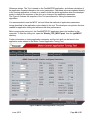
FTM0_PWMLOAD = FTM_PWMLOAD_LDOK_MASK;
It is necessary to write the LDOK bit every time the value registers are changed, not only
at the initial stage of loading them with values, but with every update after the duty cycle
value is computed in the vector control algorithm.
As mentioned in section 4.3.4, in the application, hardware triggering of the A/D converter
is employed. The Initialization Trigger signal from the FlexTimer is used as the primary
triggering signal, which is fed into the Programmable Delay Block that services the timing
of the AD conversion initiation.
FTM0_EXTTRIG |= FTM_EXTTRIG_INITTRIGEN_MASK;
Finally, the output pins of the MCU have to be configured in order to send the signals out
of the chip. The assignment of signals to output pins is set in the Pin Control Register,
while the available signals are listed in the Signal Multiplexing chapter of [1] and are
package dependent.
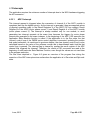
PORTC_PCR1 = PORT_PCR_MUX(4); // FTM0 CH0
PORTC_PCR2 = PORT_PCR_MUX(4); // FTM0 CH1
PORTC_PCR3 = PORT_PCR_MUX(4); // FTM0 CH2
PORTA_PCR6 = PORT_PCR_MUX(3); // FTM0 CH3
PORTA_PCR7 = PORT_PCR_MUX(3); // FTM0 CH4
June, 2013
Page 21 of 55