1
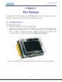
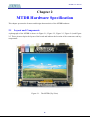
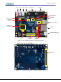
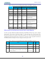
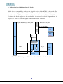
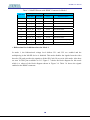
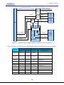
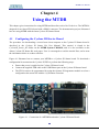
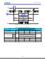
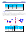
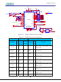
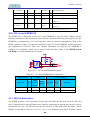
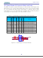
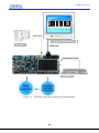
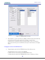
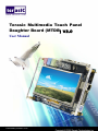
Terasic Multimedia Touch Panel Daughter Board Terasic Multimedia Touch Panel Daughter Board (MTDB) V2.0 User Manual Preliminary Version 2.00 Terasic Multimedia Touch Panel Daughter Board CONTENTS Chapter 1 The Package......................................................................................................................1 1.1 1.2 Package Contents .................................................................................................................1 Getting Help.........................................................................................................................2 Chapter 2 MTDB Hardware Specification ......................................................................................3 2.1 2.2 Layout and Components ......................................................................................................3 Block Diagram of the MTDB ..............................................................................................6 Chapter 3 MTDB Bus Controller ...................................................................................................10 3.1 3.2 3.3 3.4 MTDB Bus Controller Introduction...................................................................................10 Block Design of the MTDB Bus Controller ......................................................................10 Timing Protocol of the LCD TDM Controller ................................................................... 11 Level Translators and MAX II Mode Control Register .....................................................12 Chapter 4 Using the MTDB ............................................................................................................20 4.1 4.2 4.3 4.4 4.5 4.6 4.7 4.8 4.9 4.10 4.11 4.12 Configuring the Cyclone III Starter Board ........................................................................20 Connecting MTDB Board with the Altera DE3 Board ......................................................21 Using the 4.3” LCD Touch Panel Module .........................................................................21 Using VGA ........................................................................................................................26 Using the 24-bit Audio CODEC ........................................................................................29 RS-232 Serial Port .............................................................................................................30 PS/2 Serial Port ..................................................................................................................31 Ethernet Physical Layer Transceiver..................................................................................32 Digital Video Decoder .......................................................................................................33 I2C Serial EEPROM ..........................................................................................................35 SD Card Interface...............................................................................................................35 General Purpose I/O Connector (Mode 1 and 2 only) .......................................................37 Chapter 5 Examples of Advanced Demonstration ........................................................................38 5.1 5.2 5.3 5.4 SD Card Music Player........................................................................................................38 Music Synthesizer Demonstration .....................................................................................42 LCD TV Demonstration.....................................................................................................46 VGA TV Demonstration ....................................................................................................48 Chapter 6 Appendix .........................................................................................................................51 6.1 6.2 EEPROM and Mode Switch Utility...................................................................................51 Revision History ................................................................................................................53 ii MTDB User Manual Chapter 1 The Package The Multimedia Touch Panel Daughter board (MTDB) package contains all components needed for MTDB in conjunction with an Altera FPGA board with HSMC connector. 1.1 Package Contents The MTDB package includes: The Terasic Multimedia Touch Panel daughter board [Optional] Components to assemble the MTDB with a Cyclone III Starter Board into a BRICK format as shown in Figure 1.1. The detailed instructions on how to assemble MTDB with a Cyclone III Starter board into a BRICK format can be found in the CycloneIII_Starter_Board/BRICK folder of the MTDB System CD-ROM Figure 1.1. The BRICK form of combining the MTDB to an Altera Cyclone III Starter Board. 1 MTDB User Manual 1.2 Getting Help Here are the addresses where you can get help if you encounter problems: Terasic Technologies No. 356, Sec. 1, Fusing E. Rd. Jhubei City, HsinChu County, Taiwan, 302 Email: [email protected] Web: www.terasic.com 2 MTDB User Manual Chapter 2 MTDB Hardware Specification This chapter presents the features and design characteristics of the MTDB hardware. 2.1 Layout and Components A photograph of the MTDB is shown in Figure 2.1, Figure 2.2, Figure 2.3, Figure 2.4, and Figure 2.5. These pictures depict the layout of the board and indicate the location of the connectors and key components. Figure 2.1. The MTDB (Top View) 3 MTDB User Manual Figure 2.2. The MTDB (Connector view 1) Figure 2.3. The MTDB (Connector view 2) 4 MTDB User Manual Mic in Line in Line Out Video in RS-232 Port VGA Video Port VGA 10-bit DAC GPIO Header 24-bit Audio Codec Video Decoder (NTSC/PAL) Ethernet 10/100M Port Altera MAX II 2210 CPLD device SD Card Slot PS/2 Keyboard/Mouse Port Ethernet 10/100M PHY 100-MHz Oscillator LCD Touch Panel Connector EEPROM Figure 2.4 The MTDB PCB and Component diagram HSMC Connector Figure 2.5. The MTDB Back side – HSMC connector view 5 MTDB User Manual The MTDB board has many features that allow users to implement a wide range of designed circuits, from simple circuits to various multimedia projects with touch panel applications. The following hardware is provided on the MTDB board: Altera MAX II 2210 CPLD device SD Card socket 100-MHz oscillator for clock sources 24-bit CD-quality audio CODEC with line-in, line-out, and microphone-in jacks VGA DAC (10-bit high-speed triple DACs) with VGA-out connector Video decoder (NTSC/PAL/SECAM) and TV-in connector 10/100M Ethernet Physical Layer Transceiver RS-232 transceiver and 9-pin connector PS/2 mouse/keyboard connector 800x480 Active matrix color TFT LCD Touch Panel module I2C Serial EEPROM General Purpose I/O To use the MTDB, the user has to be familiar with the Quartus II software. 2.2 Block Diagram of the MTDB Figure 2.6 gives the block diagram of the MTDB. To provide maximum flexibility for the user, all connections are made through the HSMC connector device. Thus, the user can configure the FPGA on the mother board to implement any system design. 6 MTDB User Manual MAXII CPLD & Level Shift 24-bit AUDIO CODEC VGA 10-bit Video DAC Video decoder PS2 & RS232 Ports HSMC Connector BUS Controller LCD Touch Panel module 10/100 Ethernet PHY SD Card I2C EEPROM GPIO Header 100M Hz OSC Figure 2.6. Block diagram of the MTDB board. Following is more detailed information about the blocks in Figure 2.6: MAX II 2210 CPLD 2210 LEs 272 user IO pins FineLine BGA 324-pin package 4.3” 800x480 LCD Touch panel Module and Touch Screen Digitizer Equipped with Toppoly TD043MTEA1 active matrix color TFT LCD module. Uses the Analog Devices AD7843 touch screen digitizer Support 24-bit parallel RGB interface. 3-wire register control for display and function selection. Built-in contrast, brightness and gamma modulation. 7 MTDB User Manual SD card socket Accessible as memory in both SPI and 4-bit SD modes. Clock inputs 100-MHz oscillator. Audio CODEC Wolfson WM8731 24-bit sigma-delta audio CODEC. Line-level input, line-level output, and microphone input jacks. Sampling frequency: 8 to 96 KHz. Applications for MP3 players and recorders, PDAs, smart phones, voice recorders, etc. VGA output Uses the ADV7123 140-MHz triple 10-bit high-speed video DAC. With 15-pin high-density D-sub connector. NTSC/PAL Video decoder circuit Uses the ADV7180 Multi-format SDTV Video Decoder. Supports worldwide NTSC/PAL/SECAM color demodulation. One 10-bit ADC, 4X over-sampling for CVBS. Supports Composite Video (CVBS) RCA jack input. Supports digital output formats : 8-bit ITU-R BT.656 YCrCb 4:2:2 output + HS, VS, and FIELD Applications: DVD recorders, LCD TV, Set-top boxes, Digital TV, and Portable video devices Ethernet Physical Layer Transceiver Uses the DP83848C Single Port 10/100M Ethernet Physical Layer Transceiver Supports both 100Base-T and 10Base-T Ethernet protocols Supports Auto-MDIX for 10/100M Serial ports One RS-232 port One PS/2 port DB-9 serial connector for the RS-232 port PS/2 connector for connecting a PS2 mouse or keyboard to the MTDB board. 8 MTDB User Manual I2C serial EEPROM Use one 128-bit EEPROM. Supports 2-wire serial interface, I2C compatible. General Purpose I/O 8 general purpose I/O pins, as well as 3.3 volt power and ground line. 9 MTDB User Manual Chapter 3 MTDB Bus Controller The MTDB comes with a bus controller that allows user to access all components on the board through the HSMC connector, without being limited by the number of user I/Os of the HSMC connector. This chapter describes its structure in block diagram form, and finally describes its capabilities. 3.1 MTDB Bus Controller Introduction The two major functions of the MTDB Bus Controller are listed 1. Provide time-division multiplexing functions to the LCD and VGA color data bus. 2. Provide level shifting feature for the 2.5V (Cyclone III FPGA) and 3.3V (the MTDB side) domains. 3.2 Block Design of the MTDB Bus Controller Figure 3.1 shows the block diagram of MTDB Bus Controller. Both the LCD and VGA TDM blocks are simple 8-bit to 24-bit and 10-bit to 30-bit data de-multiplexing functions respectively, which are final logic driving the LCD panel and VGA DAC. In the LCD TDM block, the 8-bit input data (successive BGR color data) comes in at 3 times the rate of the 24-bit output data bus (8-bit B + 8bit G + 8bit R) we drive to the LCD panel. This function can reduce the pin-count of the HSMC connector. The I2C_Bir_bus block provides bidirectional control for I2C Serial EEPROM data bus. 10 MTDB User Manual LCD Touch Panel & AD converter Serial Port Interface MAXII CPLD LCD R data LCD G data LCD Color Data Bus (RGB) LCD Timing Control Bus LCD TDM Controller LCD Timing Control Bus VGA Color Data Bus (RGB) VGA Timing Control Bus HSMC Connector I2C EEPROM Interface LCD Touch Panel Module LCD B data VGA TDM Controller VGA R data VGA G data VGA B data VGA DAC VGA Timing Control Bus I2C_bir_bus Controller I2C EEPROM Other uni-directional I/Os AUDIO DAC Mode Register Logic Ethernet PHY Bi-directional I/Os Bi-directional Level Translator(U10,U11) SD Card Soket RS232 / PS/2 Ports Video Decoder GPIO Figure 3.1. The Block Diagram of MTDB Bus Controller 3.3 Timing Protocol of the LCD TDM Controller Figure 3.2 describes the input timing waveform information of the LCD TDM Controller. The 8-bit wide HC_LCD_DATA signal is presumed to contain a stream of color pixel data, with each pixel represented by three successive clock-cycles of the stream. The data is presented as "BGR". The LCD TDM Controller uses the HC_HD pulse to determine the position of the BLUE color sample, and thus the start of each three-clock pixel-period. State transitions on HC_HD (0-->1 or 1-->0) coincide with the presentation of BLUE color on the HC_LCD_DATA input. The GREEN and RED values for that same pixel are presented on the next two clock-cycles. Figure 3.3 shows the timing information from the output side. The LCD TDM block will generate a NCLK clock and 24-bit RGB data to the LCD panel. The NCLK signal runs at 1/3 frequency of the incoming clock HC_NCLK. In addition, the timing protocol of the VGA TDM controller is very similar to the LCD TDM controller. The input color data bus HC_VGA_DATA changes from 8-bit to 10-bit, and the VGA TDM controller uses the HC_VGA_HS to determine the position of the BLUE color sample. . 11 MTDB User Manual Figure 3.2. The timing diagram shows the input side of the VGA TDM Controller Figure 3.3. The timing diagram shows the output side of the LCD TDM Controller 3.4 Level Translators and MAX II Mode Control Register Bidirectional level shift interface (U10, U11, U12) There are 3 bidirectional level shifters on the board (U10, U11, and U12). These chips are all Texas Instruments TXB0108 or TXB0104 devices. U10 is used completely as bi-directional level-shifters from 2.5V input (Cyclone III FPGA) to 3.3V required by many of the interface chips. U11 and U12, however, are also used to multiplex signals based on the setting of the mode-select logic register. Figure 3.4 shows the block diagram and signals for the combination of the HSMC connector, the MAX II device and the level-shifters. Figure 3.5 shows the Level Shift Interface schematic. Table 3.1 shows the pinouts of level shift interface with HSMC connector for U11 (straight level shifting). 12 MTDB User Manual HC_PS2_CLK, HC_PS2_DAT HC_MDIO, HC_SDA, HC_I2C, HC_I2C_SDAT PS2_CLK, PS2_DAT MDIO, SDA, I2C, I2C_SDAT Bi-Dir Level Shifter (U10) SD_(DAT, DAT3, CMD) SD_D 1-2 SD_DAT 1-2 BLS (U12) GPIO_2-7 GPIO_0-1 BLS (U11) SD Card (J4) GPIO_2-7 GPIO (J13) GPIO_0-1 HSMC(J6) Enable Enable Mode Register Logic Enable TD_D0-7 or SD_D 1-2 + GPIO 2_7 TD_D0-7 Enable TD_VS, HS or GPIO_0-1 Video Decode (U8) TD_VS,HS ID_I2C MAX II (U4) Figure 3.4. Block Diagram of Bidirectional Level Shift Interface and MAX II Control VCCA VCCA VCCA Figure 3.5. Level Shift Interface Schematic. 13 MTDB User Manual Table 3.1 Device U11 Level Shift Interface Pinouts with HSMC Connector Signal Name Interface Device HSMC PIN# HSMC Side Device Side Pin # HC_I2C_SDAT I2C_SDAT U1.27,U8.33 Signal Description I2C data to audio codec and video 33 decoder. 43 HC_PS2_CLK PS2_CLK J9.6 PS/2 Clock 47 HC_PS2_DAT PS2_DAT J9.1 PS/2 Data 49 HC_MDIO MDIO U2.30 Ethernet PHY Management Data I/O SD 1-bit Mode: Card Detect 53 HC_SD_DAT3 SD_DAT3 J4.1 SD 4-bit Mode: Data3 SPI Mode: Chip Select (Active Low) SD 1-bit Mode: Command Line 44 HC_SD_CMD SD_CMD J4.2 SD 4-bit Mode: Command Line SPI Mode: Data In SD 1-bit Mode: Data Line 48 HC_SD_DAT SD_DAT J4.7 SD 4-bit Mode: Data0 SPI Mode: Data Out 50 HC_SDA SDA J10.44 LCD 3-Wire Serial Interface Data Bidirectional level shift interfaces and the Mode Control Registers In order to provide additional peripheral flexibility, the MTDB provides the user with 3 separate pinout modes. These modes as described in Table 3.2, affect the usage of the Video Decoder (U8), the SD-Card Connector (J4), and the 10-pin GPIO connector (J13). This section describes the mode configuration details and signals that are affected for each mode. Chapter Appendix describes the EEPROM and Mode-Settings tool used to change the mode register value. Table 3.2 Device U11 Level Shift Interface Pinouts with HSMC Connector Mode Action Video Decoder GPIO SD Card Enabled 0 1-bit Disabled 8 4-bit 2 1-bit Register Video decoder in standard x8 operating mode. SD Card in 1-bit 0 mode. No GPIO. 1 Video decoder disabled. 8 GPIO available. SD-Card in 4-bit mode. Video decoder enabled, but Vertical Sync (VS) and Horizontal Sync Enabled but no VS 2 (HS) pins disabled. 2 GPIO pins available - others are disabled. or HS signals SD-Card in 1-bit mode. 14 MTDB User Manual Bidirectional level shift interfaces for Mode 0 Mode 0 is the compatibility mode for the original version of the MTDB. In this mode, The bidirectional voltage level shifters U11 and U12 are disabled, and the SD-Card (J4) has a 1-bit interface, there no GPIO pins available on J13, and the video decoder (U8) is enabled. Figure 3.6 shows the block diagram for this mode which is a subset of the block diagram shown in Figure 3.4. Table 3.3 shows the signals enabled to the HSMC connector. HC_PS2_CLK, HC_PS2_DAT HC_MDIO, HC_SDA, HC_I2C, HC_I2C_SDAT Bi-Dir Level Shifter (U10) PS2_CLK, PS2_DAT MDIO, SDA, I2C, I2C_SDAT SD_(DAT, DAT3, CMD) SD Card (J4) 1-bit BLS (U12) GPIO (J13) 0 Pins BLS (U11) HSMC(J6) Disable Disable Mode Register Logic Enable TD_D0-7 TD_D0-7 Enable TD_VS, HS Video Decode (U8) TD_VS,HS ID_I2C MAX II (U4) Figure 3.6. Block Diagram of Bidirectional Level Shift Interface for Mode 0 15 MTDB User Manual Table 3.3 MAXII Pinouts with HSMC Connector in Mode 0 Signal Name Interface Device HSMC PIN# HSMC Side Device Side Pin # Signal Description 56 HC_TD_D0 TD_D0 U4.V8 Video decoder data0 60 HC_TD_D1 TD_D1 U4.T8 Video decoder data1 62 HC_TD_D2 TD_D2 U4.T9 Video decoder data2 66 HC_TD_D3 TD_D3 U4.V9 Video decoder data3 68 HC_TD_D4 TD_D4 U4.U9 Video decoder data4 72 HC_TD_D5 TD_D5 U4.U10 Video decoder data5 74 HC_TD_D6 TD_D6 U4.V10 Video decoder data6 78 HC_TD_D7 TD_D7 U4.T10 Video decoder data7 84 HC_TD_VS TD_D8 U4.V11 Video decoder vertical sync signal 86 HC_TD_HS TD_D9 U4.T11 Video decoder horizontal sync signal Bidirectional level shift interfaces for Mode 1 In mode 1, the bidirectional voltage level shifters U11 and U12 are enabled and the multiplexing in the MAXII device is disabled. This mode disables the signals from the video decoder (U8) and provides the signals to all the SD-Card (J4) to run in 4-bit mode. Also there are now 8 GPIO pins available on J13. Figure 3.7 shows the block diagram for this mode which is a subset of the block diagram shown in Figure 3.4. Table 3.4 shows the signals enabled to the HSMC connector. 16 MTDB User Manual HC_PS2_CLK, HC_PS2_DAT HC_MDIO, HC_SDA, HC_I2C, HC_I2C_SDAT PS2_CLK, PS2_DAT MDIO, SDA, I2C, I2C_SDAT Bi-Dir Level Shifter (U10) SD_(DAT, DAT3, CMD) SD_D 1-2 SD_DAT 1-2 BLS (U12) GPIO_2-7 GPIO_0-1 BLS (U11) SD Card (J4) 4-bit GPIO_2-7 GPIO_0-1 GPIO (J13) 8 Pins HSMC(J6) Enable Enable Mode Register Logic Disable SD_D 1-2 + GPIO 2_7 TD_D0-7 Disable GPIO_0-1 TD_VS,HS Video Decode (U8) Disabled ID_I2C MAX II (U4) Figure 3.7. Block Diagram of Bidirectional Level Shift Interface for Mode 1 Table 3.4 Device U11 and U12 Level Shift Interface Pinouts with HSMC Connector in Mode 1 Signal Name Interface Device HSMC PIN# HSMC Side Device Side Pin # HC_TD_D0 SD_DAT1 U12.20 Signal Description SD-Card data bus signal 1 for 4-bit 56 mode SD-Card data bus signal 2 for 4-bit 60 HC_TD_D1 SD_DAT2 U12.18 mode 62 HC_TD_D2 DBG_D2 U12.17 GPIO data pin 2 66 HC_TD_D3 DBG_D3 U12.16 GPIO data pin 3 68 HC_TD_D4 DBG_D4 U12.15 GPIO data pin 4 72 HC_TD_D5 DBG_D5 U12.14 GPIO data pin 5 74 HC_TD_D6 DBG_D6 U12.13 GPIO data pin 6 78 HC_TD_D7 DBG_D7 U12.12 GPIO data pin 7 84 HC_TD_VS DBG_D1 U11.12 GPIO data pin 1 86 HC_TD_HS DBG_D0 U11.13 GPIO data pin 0 17 MTDB User Manual Bidirectional level shift interfaces for Mode 2 In mode 2, the bidirectional voltage level shifter U11 is enabled, allowing GPIO signals 0 and 1 to propagate to the GPIO Header (J13). The complementary multiplexer in the MAX II device disables the vertical sync and horizontal sync signals from the video decoder chip (U8) from propagating. Also in this mode U12 is disabled thus GPIO signals 2 – 7 are not available on the GPIO header (J13), but the complementary multiplexer in the MAX II device enables the propagation of the data bus signals 0 – 7 from the video decoder (U8) to the HSMC connector (J6). Figure 3.8 shows the block diagram for this mode which is a subset of the block diagram shown in Figure 3.4. Table 3.5 shows the signals enabled to the HSMC connector. HC_PS2_CLK, HC_PS2_DAT HC_MDIO, HC_SDA, HC_I2C, HC_I2C_SDAT PS2_CLK, PS2_DAT MDIO, SDA, I2C, I2C_SDAT Bi-Dir Level Shifter (U10) SD_(DAT, DAT3, CMD) SD Card (J4) 1-bit BLS (U12) GPIO_0-1 BLS (U11) GPIO_0-1 GPIO (J13) 2 Pins HSMC(J6) Disable Enable Mode Register Logic Enable TD_D0-7 TD_D0-7 Disable GPIO_0-1 TD_VS,HS Video Decode (U8) VS, HS Disabled ID_I2C MAX II (U4) Figure 3.8. Block Diagram of Bidirectional Level Shift Interface for Mode 2 18 MTDB User Manual Table 3.5 MAX II and U11 Device Pinouts with HSMC Connector in Mode 2 Signal Name Interface Device HSMC PIN# HSMC Side Device Side Pin # 56 HC_TD_D0 TD_D0 U4.V8 Video decoder data0 60 HC_TD_D1 TD_D1 U4.T8 Video decoder data1 62 HC_TD_D2 TD_D2 U4.T9 Video decoder data2 66 HC_TD_D3 TD_D3 U4.V9 Video decoder data3 68 HC_TD_D4 TD_D4 U4.U9 Video decoder data4 72 HC_TD_D5 TD_D5 U4.U10 Video decoder data5 74 HC_TD_D6 TD_D6 U4.V10 Video decoder data6 78 HC_TD_D7 TD_D7 U4.T10 Video decoder data7 84 HC_TD_VS DBG_D1 U11.12 GPIO data pin 1 86 HC_TD_HS DBG_D0 U11.13 GPIO data pin 0 19 Signal Description MTDB User Manual Chapter 4 Using the MTDB This chapter gives instructions for using MTDB and describes each of its IO devices. The MTDB is designed for an Altera FPGA board with a HSMC connector. The demonstration projects illustrated here are using MTDB with the latest Cyclone III Starter Board. 4.1 Configuring the Cyclone III Starter Board The procedure for downloading a circuit from a host computer to the Cyclone III Starter board is described in the Cyclone III Starter Kit User Manual. This tutorial is found in the CycloneIII_Starter_Kit folder on the MTDB System CD-ROM, and it is also available on the Altera Cyclone III Starter Kit web pages. User is encouraged to read the tutorial first, and to treat the information below as a short reference. Figure 4.1 illustrates how to connect your MTDB to a Cyclone III Starter board. To download a configuration bit stream into the Cyclone III FPGA, perform the following steps: Ensure that power is applied to the Cyclone III Starter board Connect the supplied USB cable to the USB Blaster port on the Cyclone III Starter board The FPGA can now be programmed by using the Quartus II Programmer module to select a configuration bit stream file with the .sof filename extension Figure 4.1. Connection of a MTDB Board and a Cyclone III Starter Board. 20 MTDB User Manual Users can find the default demonstration project under the Demonstrations/default folder in the MTDB System CD-ROM. Users are also encouraged to examine the top-level RTL code when reading the following sections. 4.2 Connecting MTDB Board with the Altera DE3 Board To connect the MTDB board with the Altera DE3 board, please refer to the How_to_connect_MTDB_to_DE3.pdf which can be available from the directory “Using_MTDB_on_DE3” in the MTDB SYSTEM CD. 4.3 Using the 4.3” LCD Touch Panel Module The MTDB provides a 4.3" Toppoly TD043MTEA1 active matrix color TFT LCD panel. The LCD Touch Panel module has the highest resolution (800x480) to provide users the best display quality for developing applications. The LCD panel supports 24-bit parallel RGB data interface and provides 3-wire serial port interface to control the display function registers. The MTDB Board is also equipped with an Analog Devices AD7843 touch screen digitizer chip. The AD7843 is a 12-bit analog to digital converter (ADC) for digitizing x and y coordinates of touch points applied to the touch screen. Also, the coordinates of the touch point can be read through the serial port interface on the AD7843. However, because of limited IOs of the HSMC connector, the clock signal of the serial port interface for the LCD panel and AD7843 share the same HSMC connector IO called HC_ADC_DCLK, users must not control both LCD panel and AD7843 at the same time. To display images on the LCD panel correctly, the first thing users need to do is that the RGB color data and synchronization signals need to follow the timing specification of the LCD Touch panel as shown in Figure 4.2, Figure 4.3, Table 4.1, and Table 4.2. Further more, because the number of user IOs of the HSMC connector are limited, the LCD RGB data and synchronization signals outputted to the MTDB board need to be multiplex to fit the input timing specification of the LCD TDM Controller on the MTDB board as mention in the Section 3.3. Finally, the associated schematic of the LCD touch panel module is given in Figure 4.4, and the pin assignments are listed in Table 4.3. Detailed information for using the LCD panel and AD7843 are available in their datasheets, which can be found in the Datasheet folder of the MTDB System CD-ROM or from the manufacturers' web site. 21 MTDB User Manual Figure 4.2 LCD horizontal timing specification Table 4.1 LCD horizontal timing parameters Panel Resolution Parameter Symbol Unit 800xRGBx480 480xRGBx272 400xRGBx240 NCLK Frequency FNCLK 33.2 9 8.3 MHz Horizontal valid data thd 800 480 400 NCLK 1 Horizontal Line th 1056 525 528 NCLK Min. HSYNC Pulse Width Typ. 1 thpw NCLK - Max. - Hsync back porch thbp 216 43 108 NCLK Hsync front porch thfp 40 2 20 NCLK DEN Enable Time tep 800 480 400 NCLK 22 MTDB User Manual Figure 4.3 LCD vertical timing specification Table 4.2 LCD vertical timing parameters Panel Resolution Parameter Symbol Unit 800xRGBx480 480xRGBx272 400xRGBx240 Vertical valid data tvd 480 272 240 H Vertical period tv 525 286 262 H Min. VSYNC Pulse Width Typ. 1 tvpw H - Max. - Vertical back porch tvbo 35 12 20 H Vertical front porch tvfpo 10 2 2 H Vertical blanking tvb 45 14 22 H 23 MTDB User Manual J10 U6 1 10 B[0..7] +VCC +VCC X_RIGHT X_LEFT 2 4 X+ X- Y_TOP Y_BOTTOM 3 5 Y+ Y- 7 8 IN3 IN4 6 GND DCLK 16 ADC_DCLK CS 15 ADC_CS_n DIN 14 ADC_DIN BUSY 13 ADC_BUSY DOUT 12 ADC_DOUT PENIRQ 11 ADC_PENIRQ_n R57 33 9 VREF CGH CPL1 CPL2 VCOM VD HD DEN NCLK B0 B1 B2 B3 B4 B5 B6 B7 VCC33 U7 AD7843 V+ 1 3 TRIM 2 G0 G1 G2 G3 G4 G5 G6 G7 V- ADR525 VCC33 VCC33 R58 10K HVDE R59 10K SDA R60 10K ADC_PENIRQ_n R61 10K ADC_CS_n R62 10K SCEN C31 CGH 2.2U C33 VCOM 2.2U C34 2.2U C35 VDDP 2.2U C36 VDDN 2.2U C37 2.2U +5V -5V VCC33 C42 10N C43 10N C44 10N C45 Y_BOTTOM 10N X_RIGHT FB VMP VMN C11 C12 CGL Y_TOP X_LEFT Y_BOTTOM X_RIGHT VCC33 Y_TOP X_LEFT VDDN 2.2U C39 VMN 2.2U C41 CGL 2.2U LED_B+ LED_B- PMEG2010ABE 1 2 3 4 5 6 7 8 9 10 11 12 13 14 15 16 17 18 19 20 21 22 23 24 25 26 27 28 29 30 31 32 33 34 35 36 37 38 39 40 41 42 43 44 45 46 47 48 49 50 51 52 53 54 55 56 57 58 59 60 GND VCC VDDP VDDN SCL VCC GND LED B+ LED B- 61 61 D5 C38 VMP R0 R1 R2 R3 R4 R5 R6 R7 VDDP TP_AGND VDDN HVDE GREST STBY SCEN ADC_DCLK SDA 1 2 3 4 5 6 7 8 9 10 11 12 13 14 15 16 17 18 19 20 21 22 23 24 25 26 27 28 29 30 31 32 33 34 35 36 37 38 39 40 41 42 43 44 45 46 47 48 49 50 51 52 53 54 55 56 57 58 59 60 62 VCC33 G[0..7] 62 R[0..7] FPC-60B_CONNECTOR Figure 4.4. Schematic diagram of the LCD Touch Panel Module Table 4.3. Pin assignments for the LCD Touch Panel Module HSMC Connector MAX II LCD Touch Panel HSMC Pin Signal Name Device Connector No. Signal Name Pin No. Description Side Pin Side Pin HC_VD 132 D14 F6 VD 6 LCD Vertical Sync Input HC_HD 134 C14 F5 HD 7 LCD Horizontal Sync Input HC_DEN 138 C15 E5 DEN 8 LCD RGB Data Enable HC_NCLK 95 K13 E4 NCLK 9 LC D Clock H1 R[0] 28 LCD red data bus bit 0 E3 G[0] 19 LCD green data bus bit 0 D4 B[0] 10 LCD blue data bus bit 0 H2 R[1] 29 LCD red data bus bit 1 HC_LCD_DATA[0] HC_LCD_DATA[1] 145 149 D17 C17 24 MTDB User Manual HC_LCD_DATA[2] HC_LCD_DATA[3] HC_LCD_DATA[4] HC_LCD_DATA[5] HC_LCD_DATA[6] HC_LCD_DATA[7] 151 126 128 146 150 152 C16 D13 D15 B15 B14 A15 F3 G[1] 20 LCD green data bus bit 1 C3 B[1] 11 LCD blue data bus bit 1 J2 R[2] 30 LCD red data bus bit 2 F1 G[2] 21 LCD green data bus bit 2 C2 B[2] 12 LCD blue data bus bit 2 J1 R[3] 31 LCD red data bus bit 3 F2 G[3] 22 LCD green data bus bit 3 D3 B[3] 13 LCD blue data bus bit 3 J3 R[4] 32 LCD red data bus bit 4 G2 G[4] 23 LCD green data bus bit 4 D1 B[4] 14 LCD blue data bus bit 4 K3 R[5] 33 LCD red data bus bit 5 G1 G[5] 24 LCD green data bus bit 5 D2 B[5] 15 LCD blue data bus bit 5 K1 R[6] 34 LCD red data bus bit 6 G3 G[6] 25 LCD green data bus bit 6 E2 B[6] 16 LCD blue data bus bit 6 K2 R[7] 35 LCD red data bus bit 7 H3 G[7] 26 LCD green data bus bit 7 E1 B[7] 17 LCD blue data bus bit 7 LCD Global Reset, Low Active HC_GREST 140 C13 L2 GREST 40 HC_SCEN 144 B13 L1 SCEN 42 LCD 3-Wire Serial Interface Enable U11-10 HC_SDA 50 U11-5 (*1) SDA J10.44 ADC_DCLK U6.16 LCD 3-Wire SerialInterface Data (*1) AD7843/LCD 3-Wire Serial HC_ADC_DCLK 157 B18 L3 Interface Clock AD7843 Serial Interface HC_ADC_DIN 155 B16 N2 ADC_DIN U6.14 Data In AD7843 Serial Interface HC_ADC_CS_n 143 D18 N1 ADC_CS_n U6.15 Chip Select Input AD7843 Serial Interface HC_ADC_DOUT 122 E13 M1 ADC_DOUT U6.12 Data Out HC_ADC_PENIRQ_n 156 A14 M3 ADC_PENIRQ_n U6.11 AD7843 pen Interrupt HC_ADC_BUSY E15 M2 ADC_BUSY U6.13 AD7843 Serial Interface Busy 120 Notes:(1) These signals do not go through the MAX II chip. They pass through the MAX3378 level translator chip, U11. 25 MTDB User Manual 4.4 Using VGA The MTDB includes a 16-pin D-SUB connector for VGA output. The VGA synchronization signals are provided directly from the Cyclone III FPGA, and the Analog Devices ADV7123 triple 10-bit high-speed video DAC is used to produce the analog data signals (red, green, and blue). The associated schematic is given in Figure 4.5. VGA_AVCC 560 BC43 BC44 0.1U 0.1U ADV7123 VAA B0 B1 B2 B3 B4 B5 B6 B7 B8 B9 CLOCK G0 G1 G2 G3 G4 G5 G6 G7 G8 G9 BLANK SYNC VREF COMP IOR IOR IOG IOG VAA VAA IOB IOB GND GND 36 35 34 33 32 31 30 29 28 27 26 25 J12 VGA_R VGA_G VGA_B VGA_AVCC R70 R71 R72 75 75 75 VGA_AGND VGA_AGND VGA_AGND VGA_HS R73 VGA_VS R74 47 47 1 2 3 4 5 6 7 8 9 10 11 12 13 14 15 6 1 VGA_B0 VGA_B1 VGA_B2 VGA_B3 VGA_B4 VGA_B5 VGA_B6 VGA_B7 VGA_B8 VGA_B9 VGA_CLOCK 11 10 5 16 13 14 15 16 17 18 19 20 21 22 23 24 1 2 3 4 5 6 7 8 9 10 11 12 RSET R69 R9 R8 R7 R6 R5 R4 R3 R2 R1 R0 PSAVE RSET U9 VGA_G0 VGA_G1 VGA_G2 VGA_G3 VGA_G4 VGA_G5 VGA_G6 VGA_G7 VGA_G8 VGA_G9 VGA_BLANK VGA_SYNC 4.7K 48 47 46 45 44 43 42 41 40 39 38 37 VGA_ R9 VGA_ R8 VGA_ R7 VGA_ R6 VGA_ R5 VGA_ R4 VGA_ R3 VGA_ R2 VGA_ R1 VGA_ R0 R68 15 17 VGA_R[0..9] VGA_G[0..9] VGA_B[0..9] VGA VGA_AGND VGA_AVCC Figure 4.5. VGA circuit schematic. The timing specification for VGA synchronization and RGB (red, green, blue) data can be found on various educational web sites (for example, search for “VGA signal timing”). Figure 4.6 illustrates the basic timing requirements for each row (horizontal) that is displayed on a VGA monitor. An active-low pulse of specific duration (time a in the figure) is applied to the horizontal synchronization (hsync) input of the monitor, which signifies the end of one row of data and the start of the next. The data (RGB) inputs on the monitor must be off (driven to 0 V) for a time period called the back porch (b) after the hsync pulse occurs, which is followed by the display interval (c). During the data display interval the RGB data drives each pixel in turn across the row being displayed. Finally, there is a time period called the front porch (d) where the RGB signals must again be off before the next hsync pulse coming up. The timing of the vertical synchronization (vsync) is same as shown in Figure 4.6, except that a vsync pulse signifies the end of one frame and the start of the next. The data refers to a set of rows in the frame (horizontal timing). Table 4.4 and Table 4.5 show the durations of time periods a, b, c, and d for both horizontal and vertical timing at different resolution. Since the number of user IOs of the HSMC connector are limited, users need to multiplex the VGA synchronization signals and RGB data to fit the input timing specification of the VGA TDM block as mentioned in Section 3.3. 26 MTDB User Manual Detailed information for using the ADV7123 video DAC is available in its datasheet, which can be found on the manufacturer's web site, and from the Datasheet folder of the MTDB System CD-ROM. The pin assignments are listed in Table 4.6. An example of code that drives a VGA display is described in Sections 5.2 and 5.3. Back porch b Front porch d Display interval c DATA HSYNC Sync a Figure 4.6. VGA horizontal timing specification. Table 4.4. VGA horizontal timing specification. VGA mode Horizontal Timing Spec Configuration Resolution(HxV) a(us) b(us) c(us) d(us) Pixel clock(Mhz) VGA(60Hz) 640x480 3.8 1.9 25.4 0.6 25 (640/c) VGA(85Hz) 640x480 1.6 2.2 17.8 1.6 36 (640/c) SVGA(60Hz) 800x600 3.2 2.2 20 1 40 (800/c) SVGA(75Hz) 800x600 1.6 3.2 16.2 0.3 49 (800/c) SVGA(85Hz) 800x600 1.1 2.7 14.2 0.6 56 (800/c) XGA(60Hz) 1024x768 2.1 2.5 15.8 0.4 65 (1024/c) XGA(70Hz) 1024x768 1.8 1.9 13.7 0.3 75 (1024/c) XGA(85Hz) 1024x768 1.0 2.2 10.8 0.5 95 (1024/c) 1280x1024(60Hz) 1280x1024 1.0 2.3 11.9 0.4 108 (1280/c) Table 4.5. VGA vertical timing specification. VGA mode Configuration Vertical Timing Spec Resolution (HxV) a(lines) b(lines) c(lines) d(lines) VGA(60Hz) 640x480 2 33 480 10 VGA(85Hz) 640x480 3 25 480 1 SVGA(60Hz) 800x600 4 23 600 1 SVGA(75Hz) 800x600 3 21 600 1 SVGA(85Hz) 800x600 3 27 600 1 XGA(60Hz) 1024x768 6 29 768 3 XGA(70Hz) 1024x768 6 29 768 3 XGA(85Hz) 1024x768 3 36 768 1 1280x1024(60Hz) 1280x1024 3 38 1024 1 27 MTDB User Manual Table 4.6. ADV7123 pin assignments. HSMC Connector MAX II VGA DAC Interface HSMC Pin Signal Name Device Pin Connector No. Signal Name Description Side Pin No. Side Pin HC_VGA_DATA[0] HC_VGA_DATA[1] HC_VGA_DATA[2] HC_VGA_DATA[3] HC_VGA_DATA[4] HC_VGA_DATA[5] HC_VGA_DATA[6] HC_VGA_DATA[7] HC_VGA_DATA[8] HC_VGA_DATA[9] 65 67 71 73 77 79 83 85 89 91 N16 M16 M18 M17 L17 L18 L16 K16 K18 J18 U7 VGA_R0 39 VGA red data bus bit 0 V4 VGA_G0 1 VGA green data bus bit 0 R7 VGA_B0 14 VGA blue data bus bit 0 V7 VGA_R1 40 VGA red data bus bit 1 U4 VGA_G1 2 VGA green data bus bit 1 P6 VGA_B1 15 VGA blue data bus bit 1 T7 VGA_R2 41 VGA red data bus bit 2 U3 VGA_G2 3 VGA green data bus bit 2 R6 VGA_B2 16 VGA blue data bus bit 2 T6 VGA_R3 42 VGA red data bus bit 3 V2 VGA_G3 4 VGA green data bus bit 3 R5 VGA_B3 17 VGA blue data bus bit 3 V6 VGA_R4 43 VGA red data bus bit 4 P8 VGA_G4 5 VGA green data bus bit 4 N4 VGA_B4 18 VGA blue data bus bit 4 U6 VGA_R5 44 VGA red data bus bit 5 R9 VGA_G5 6 VGA green data bus bit 5 N5 VGA_B5 19 VGA blue data bus bit 5 U5 VGA_R6 45 VGA red data bus bit 6 P9 VGA_G6 7 VGA green data bus bit 6 M5 VGA_B6 20 VGA blue data bus bit 6 V5 VGA_R7 46 VGA red data bus bit 7 P10 VGA_G7 8 VGA green data bus bit 7 M4 VGA_B7 21 VGA blue data bus bit 7 T5 VGA_R8 47 VGA red data bus bit 8 R10 VGA_G8 9 VGA green data bus bit 8 M6 VGA_B8 22 VGA blue data bus bit 8 T4 VGA_R9 48 VGA red data bus bit 9 P11 VGA_G9 10 VGA green data bus bit 9 L6 VGA_B9 23 VGA blue data bus bit 9 HC_VGA_BLANK 59 N17 R8 VGA_BLANK 11 VGA BLANK HC_VGA_HS 54 M13 K5 VGA_HS 13 VGA Horizontal Sync Input HC_VGA_VS 55 P17 L5 VGA_VS 14 VGA Vertical Sync Input 28 MTDB User Manual HC_VGA_SYNC 61 N18 P7 VGA_SYNC 12 VGA SYNC HC_VGA_CLOCK 97 J13 L4 VGA_CLOCK 24 VGA TDM Clock 4.5 Using the 24-bit Audio CODEC The MTDB provides high-quality 24-bit audio via the Wolfson WM8731 audio CODEC (ENCoder/DECoder). This chip supports microphone-in, line-in, and line-out ports, with a sample rate adjustable from 8 kHz to 96 kHz. The WM8731 is controlled by a serial I2C bus interface, which is connected to the HSMC connector. A schematic diagram of the audio circuitry is shown in Figure 4.7, and the pin assignments are listed in Table 4.4. Detailed information for using the WM8731 codec is available in its datasheet, which can be found in the Datasheet folder of the MTDB System CD-ROM or from the manufacturers' web site. Since the direction of the signals HC_AUD_ADCLRCK, HC_AUD_DACLRCK, and HC_AUD_BLCK in the MAX II CPLD are from HSMC connector to the WM8731 codec, the WM8731 codec only works in Slave mode. If users need the WM8731 codec working in Master mode, they can modify the direction of the HC_AUD_BCLK in the MAX II CPLD RTL code, which can be found in the MTDB_Bus_Controller/default folder on the MTDB System CD-ROM. 1U C2 1U R0 4.7K R1 4.7K 5 2 4 1 3 C1 LINE IN NCL R NCR L GND J2 PHONE JACK B VCC33 VCC33 R4 R5 2K 2K R2 R3 4.7K 4.7K AGND AGND J1 28 27 26 25 24 23 22 1U WM8731 21 20 19 18 17 16 15 C4 680 10U AGND A_VCC33 C5 R8 1N 47K AGND J3 AGND AGND AGND LINE OUT PHONE JACK G 29 8 9 10 11 12 13 14 AGND R7 MBIAS VMID AGND AVDD ROUT LOUT HPGND PHONE JACK P NCL R NCR L GND XTI/MCLK XTO DCVDD DGND DBVDD CLKOUT BCLK EXPOSED DACDAT DACLRCK ADCDAT ADCLRCK HPVDD LHPOUT RHPOUT 1 2 3 4 5 6 7 5 2 4 1 3 VCC33 AUD_XCK AUD_BCLK AUD_DACDAT AUD_DACLRCK AUD_ADCDAT AUD_ADCLRCK C3 SCL K SDIN CSB MODE LLINEIN RLINEIN MICIN U1 MIC IN 330 NCL R NCR L GND R6 5 2 4 1 3 I2C_SDAT I2C_SCLK AGND TC1 100U/6.3V TC2 100U/6.3V A_VCC33 R9 R10 47K 47K AGND AGND Figure 4.7. Audio CODEC schematic. 29 AGND MTDB User Manual Table 4.7. Audio CODEC pin assignments. HSMC Connector MAX II Audio Codec HSMC Pin Signal Name Device Pin Connector No. Signal Name Description Side Pin No. Side Pin Audio CODEC HC_AUD_BCLK 113 G17 U13 AUD_BCLK 7 Bit-Stream Clock Audio CODEC Chip HC_AUD_XCK 39 T16 U14 AUD_XCK 1 Clock HC_AUD_DACDAT 109 H17 V13 AUD_DACDAT 8 HC_AUD_DACLRCK 107 H18 T13 AUD_DACLRCK 9 Audio CODEC DAC Data Audio CODEC DAC LR Clock HC_AUD_ADCDAT 40 R15 T12 AUD_ADCDAT 10 HC_AUD_ADCLRCK 103 H16 V12 AUD_ADCLRCK 11 Audio CODEC ADC Data Audio CODEC ADC LR Clock HC_I2C_SDAT 33 HC_I2C_SCLK 34 U10-2 (*1) U10-13 (*1) P15 U11 I2C_SDAT 27 I2C Data I2C_SCLK 28 I2C Clock Notes: (*1) These signals do not go through the MAX II chip. They pass through the MAX3378 level translator chip, U10. 4.6 RS-232 Serial Port The MTDB board uses the ADM3202 transceiver chip and a 9-pin D-SUB connector for RS-232 communications. For detailed information on how to use the transceiver, please refer to the datasheet, which is available in the Datasheet folder of the MTDB System CD-ROM or from the manufacturers' web site. Figure 4.8 shows the related schematics, and Table 4.8 lists the HSMC pin assignments. J8 U5 UART_RXD 12 9 11 10 UART_TXD VCC33 RXD LEDR R75 330 UART_RXD TXD LEDG R76 330 UART_TXD C27 1U C28 1U 1 3 4 5 2 6 C29 C30 1U 1U R1OUT R2OUT T1IN T2IN C+ C1C2+ C2V+ V- R1IN R2IN T1OUT T2OUT 13 8 14 7 ADM3202 VCC GND 16 15 VCC33 Figure 4.8. ADM3202 (RS-232) schematic. 30 10 11 5 9 4 8 3 7 2 6 1 RS232 MTDB User Manual Table 4.8. RS-232 pin assignments. HSMC Connector MAX II RS232 Interface HSMC Pin Device Signal Name Connector No. Signal Name Pin No. Description Side Pin Side Pin HC_UART_RXD 115 G18 K4 UART_RXD U5-12 (*1) UART Receiver HC_UART_TXD 119 G16 J4 UART_TXD U5-11 (*2) UART Transmitter Notes (*1) U5.12 connects to pin 3 on the RS-232 connector (J6) via U5.13. (*2) U5.11 connects to pin 2 on the RS-232 connector (J6) via U5.14. 4.7 PS/2 Serial Port The MTDB includes a standard PS/2 interface and a connector for a PS/2 keyboard or mouse. Figure 4.9 shows the schematic of the PS/2 circuit. Instructions for using a PS/2 mouse or keyboard can be found by performing an appropriate search on various educational web sites. The pin assignments for the associated interface are shown in Table 4.9. VCC5 VCC5 R53 R54 2K 2K J9 TOP PS2_DAT PS2_CLK R56 R55 PS2DAT 120 120 3 PS2CLK D4 BAT54S BAT54S VCC33 8 6 3 5 2 1 9 10 11 BC34 2 1 D3 2 1 3 VCC5 1 2 3 5 6 8 0.1U PS2 VCC33 Figure 4.9. PS/2 schematic. Table 4.9. PS/2 pin assignments. HSMC Connector MAX II PS/2 Interface HSMC Device Signal Name Pin No. Connector Signal Name Pin No. Description Side Pin Side Pin HC_PS2_CLK 43 U10-3 (*1) U10-18 (*1) PS2_CLK 1 PS/2 Clock HC_PS2_DAT 47 U10-4 (*1) U10-17 (*1) PS2_DAT 6 PS/2 Data Notes: (*1) These signals do not go through the MAX II chip. They pass through the MAX3378 level translator chip, U10. 31 MTDB User Manual 4.8 Ethernet Physical Layer Transceiver The MTDB board provides Ethernet support via the National Semiconductor DP83848C Ethernet Physical Layer Transceiver chip. The DP83848C is a one port Fast Ethernet PHY Transceiver supporting IEEE 802.3 physical layer applications at 10Mbps and 100Mbps. The DP83848C provides Media Independent Interface (MII) to connect DP83848C to a MAC in 10/100M systems. Figure 4.10 shows the schematic for the Ethernet Physical Layer Transceiver interface, and the associated pin assignments are listed in Table 4.10. For detailed information on how to use the DP83848C, please refer to its datasheet and application note, which are available in the Datasheet folder of the MTDB System CD-ROM or from the manufacturers' web site. VCC33 R11 VCC33 1.5K MDIO BC5 0.1U Y1 1 EN VCC 4 2 GND OUT 3 25MHZ MDC ETH_RESET_N VCC33 TXD[0..3] ACT R12 120 ACTIVITY ACTIVITY R13 120 SPEED LEDR DUPLEX 1K VCC33 100Mbps C6 BC6 SPE 10U 0.1U DUPLEX R14 DUPLEX RXD[0..3] E_AVCC33 RX_COL R19 33 RXD0 R20 33 RXD1 R21 33 R22 33 RXD3 R23 33 VCC33 C9 BC11 10U 0.1U PFBIN2 RX_CLK RX_DV/MII_MODE CRS/CRS_DV/LED_CFG RX_ER/MDIX_EN COL/PHYAD0 DP83848C RXD_0/PHYAD1 RXD_1/PHYAD2 RXD_2/PHYAD3 RXD_3/PHYAD4 IOGND IOVDD33 24 23 22 21 20 19 18 17 16 15 14 13 RBIAS PFBOUT AVDD33 RESERVED RESERVED AGND PFBIN1 TD+ TDAGND RD+ RD- E_AGND TX_CLK R31 33 TX_EN R32 33 TXD0 R33 33 TXD1 R34 33 TXD2 R35 33 TXD3 R36 33 E_AGND R25 R26 2.2K 2.2K E_AVCC33 J5 BC10 0.1U E_AGND TD+ TD- 1 2 4 5 3 6 7 8 E_AVCC33 RD+ RDE_AGND R27 49.9 R28 49.9 R29 49.9 1 2 3 4 5 6 7 8 9 10 11 12 RXD2 37 38 39 40 41 42 43 44 45 46 47 48 R30 49.9 E_AVCC33 E_AGND E_AVCC33 BC12 BC13 0.1U 0.1U E_AGND R37 2.2K E_AGND BC14 BC15 0.1U 0.1U TD+ TDCTT CTR RD+ RDNC CHSG 15 33 16 33 R18 0.1U 4.7K MNT1 R17 RX_ERR R24 BC9 10U MNT0 RX_CRS E_AGND C8 0.1U YELLOW SMNT1 33 BC8 10U SMNT0 R16 C7 14 RX_DV 0.1U TX_CLK TX_EN TXD_0 TXD_1 TXD_2 TXD_3/SNI_MODE PWR_DOWN/INT TCK TDO TMS TRST# TDI 33 DGND IOGND X1 X2 IOVDD33 MDC MDIO RESET_N LED_LINK/AN0 LED_SPEED/AN1 LED_ACT/COL/AN_EN 25MHz_OUT BC7 R15 13 U2 RX_CLK PFBOUT 36 35 34 33 32 31 30 29 28 27 26 25 PFBOUT GREEN E_AGND Fast Ethernet schematic. Table 4.10. Fast Ethernet pin assignments. HSMC Connector MAX II Ethernet PHY HSMC Pin Signal Name Device Pin Connector No. Signal Name Description Side Pin No. Side Pin HC_TX_CLK 158 A13 T2 TX_CLK 1 MII Transmit Clock HC_TX_EN 125 F18 R3 TX_EN 2 MII Transmit Enable HC_TXD[0] 127 F17 P4 TXD0 3 MII Transmit Data bit 0 HC_TXD[1] 131 E17 R1 TXD1 4 MII Transmit Data bit 1 HC_TXD[2] 133 E18 R2 TXD2 5 MII Transmit Data bit 2 HC_TXD[3] 137 E16 P2 TXD3 6 MII Transmit Data bit 3 HC_ETH_RESET_N 121 F16 T3 Eth_RESET_N 29 DP83848C Reset 32 11 D4 12 D2 10 D1 9 RJ45INTLED VCC33 Figure 4.10. D3 ACTIVITY SPEED VCC33 MTDB User Manual HC_MDIO 49 U10-5(*1) U10-16(*1) MDIO 30 Management Data IO HC_MDC 139 D16 U1 MDC 31 Management Data Clock HC_RX_CLK 96 H14 J5 RX_CLK 38 MII Receive Clock HC_RX_DV 116 E14 H5 RX_DV 39 MII Receive Data valid HC_RX_CRS 92 H15 H4 RX_CRS 40 MII Carrier Sense HC_RX_ERR 90 G13 H6 RX_ERR 41 MII Receive Error HC_RX_COL 114 F14 G6 RX_COL 42 MII Collision Detect HC_RXD[0] 102 G15 G4 RXD0 43 MII Receive Data bit 0 HC_RXD[1] 104 G12 G5 RXD1 44 MII Receive Data bit 1 HC_RXD[2] 108 F13 G7 RXD2 45 MII Receive Data bit 2 HC_RXD[3] 110 F15 F4 RXD3 46 MII Receive Data bit 3 Notes: (*1) These signals do not go through the MAX II chip. They pass through the MAX3378 level translator chip, U10. 4.9 Digital Video Decoder The MTDB is equipped with an Analog Devices ADV7180 VIDEO decoder chip. The ADV7180 is an integrated video decoder that automatically detects and converts a standard analog baseband television signal (NTSC, PAL, and SECAM) into 4:2:2 component video data, which is compatible with 8-bit CCIR601/CCIR656. The ADV7180 is compatible with a broad range of video devices, including DVD players, tape-based sources, broadcast sources, and security/surveillance cameras. The registers in the VIDEO decoder can be programmed by a serial I2C bus, which is connected to the HSMC connector as indicated in Figure 4.11. The pin assignments are listed in Table 4.11. Detailed information of the ADV7180 is available in the Datasheet folder of the MTDB System CD-ROM or from the manufacturers' web site. 33 MTDB User Manual VCC33 VCC18 AV_VCC18 PV_VCC18 R65 0.1U 39 TD_RESET 23 29 30 AIN1 AIN2 AIN3 31 RESET 26 VREFN 25 VREFP 13 XTAL 12 XTAL1 32 ALSB 18 PWRDWN V_AGND C50 0.1U C51 C52 0.1U 0.1U 28MHz I2C ADDRESS IS 0x40 VCC33 I2C_SCLK I2C_SDAT 34 33 SCLK SDATA 27 20 1 4 R63 1.74K 10N ELPF 19 P0 P1 P2 P3 P4 P5 P6 P7 17 16 10 9 8 7 6 5 VS/FIELD HS SFL 37 39 2 INTRQ LLC 38 11 TEST_0 22 ADV7180 TD_D[0..7] RN2 9 10 11 12 13 14 15 16 47 8 7 6 5 4 3 2 1 R66 R67 TD_D0 TD_D1 TD_D2 TD_D3 TD_D4 TD_D5 TD_D6 TD_D7 120 TD_VS 120 TD_HS 27MHZ VCC33 3 15 35 40 41 21 24 28 RCA JACK 36 CVBS1_IN C49 DGND DGND DGND DGND EXPOSED AGND AGND AGND R64 0.1U C47 AVDD PVDD J11 DVDDIO DVDDIO DVDD DVDD 14 36 C48 U8 BC38 Y3 1 0.1U V_AGND 2 EN VCC 4 GND OUT 3 28.63636MHz Figure 4.11. Digital VIDEO Decoder schematic. Table 4.11. VIDEO Decoder pin assignments. HSMC Connector MAX II Video Decoder HSMC Pin Signal Name Device Connector No. Pin Signal Name Side Pin Description No. Side Pin Video HC_TD_D[7] 78 K14 T10 TD_D7 Decoder Data7 (Mode Control Data7 (Mode Control Data7 (Mode Control Data7 (Mode Control Data7 (Mode Control Data7 (Mode Control Data7 (Mode Control 5 Register = 0 or 2) Video HC_TD_D[6] 74 K15 V10 TD_D6 Decoder 6 Register = 0 or 2) Video HC_TD_D[5] 72 L13 U10 TD_D5 Decoder 7 Register = 0 or 2) Video HC_TD_D[4] 68 M12 U9 TD_D4 Decoder 8 Register = 0 or 2) Video HC_TD_D[3] 66 L15 V9 TD_D3 Decoder 9 Register = 0 or 2) Video HC_TD_D[2] 62 L14 T9 TD_D2 Decoder 10 Register = 0 or 2) Video HC_TD_D[1] 60 M14 T8 TD_D1 Decoder 16 Register = 0 or 2) Video Decoder Data7 (Mode Control HC_TD_D[0] 56 M15 V8 TD_D0 17 Register = 0 or 2) HC_TD_27MHZ 98 G14 U8 TD_27MHZ 34 11 I2C Clock 28MHz MTDB User Manual HC_TD_RESET 80 J14 HC_I2C_SDAT 33 HC_I2C_SCLK HC_TD_VS U12 TD_RESET 31 Video Decoder Reset U10-2 (*1) U10-20 (*1) I2C_DATA 33 I2C Data 34 P15 U11 I2C_SCLK 34 Video Decoder Clock Input 84 J15 V11 TD_VS 37 Video Decoder V_SYNC (Mode Control Register = 0) Video Decoder H_SYNC (Mode Control HC_TD_HS 86 H13 T11 TD_HS 39 Register = 0) Notes :*(1) These signals do not go through the MAX II chip. They pass through the MAX3378 level translator chip, U10. 4.10 I2C Serial EEPROM The MTDB uses a Microchip 128-bit I2C serial EEPROM to store the MAC address and the boundary parameters of the touch panel for the Ethernet operation and touch panel respectively. The EEPROM is programmed by I2C serial Interface, which is connected through the CPLD to the HSMC connector. Figure 4.12 shows the schematic of the I2C Serial EEPROM, and the associated pin assignments are listed in Table 4.12. Detailed information for using the I2C EEPROM is available in its datasheet, which can be found in the Datasheet folder of the MTDB System CD-ROM or from the manufacturers' web site. Figure 4.12. I2C Serial EEPROM schematic. Table 4.12. I2C Serial EEPROM pin assignments. HSMC Connector MAX II I2C Serial EEPROM HSMC Pin Signal Name Device Connector No. Signal Name Pin No. Description Side Pin Side Pin HC_ID_I2CSCL 41 T17 N3 ID_I2CSCL 6 EEPROM I2C Clock HC_ID_I2CDAT 42 P18 P3 ID_I2CDAT 5 EEPROM I2C Data 4.11 SD Card Interface The MTDB includes a SD card socket and provides both SPI and SD 4-bit mode for SD Card access. Instructions for using SD card can be found by performing an appropriate search on various educational web sites. The SD-Card can also be accessed in 4-bit mode when the Mode Control Register in the MAX II Device is set to 1 (see “Level Translators and MAX II Mode Control 35 MTDB User Manual Register” and Appendix). Figure 4.13 shows the schematic of the SD card interface and the associated pin assignments are listed in Table 4.13. Figure 4.13. SD card interface schematic. Table 4.13. SD card interface pin assignments. HSMC Connector Switch Pin #s SD Card HSMC Pin Signal Name Device Connector No. Signal Name Pin No. Description Side Pin Side Pin SD 1-bit Mode: Card Detect HC_SD_DAT3 53 U10.6 J4.1 SD_DAT3 1 SD 4-bit Mode: Data3 SPI Mode: Chip Select (Active Low) SD 1-bit Mode: Command Line HC_SD_CMD 44 U10.7 J4.2 SD_CMD 2 SD 4-bit Mode: Command Line SPI Mode: Data In HC_SD_CLK 101 U4.J16 U14.P1 SD_CLK 5 Clock SD 1-bit Mode: Data Line HC_SD_DAT 48 U10.8 J4.7 SD_DAT 7 SD 4-bit Mode: Data0 SPI Mode: Data Out SD 4-bit: Data1 (MAXII Mode HC_TD_D0 56 U12.1 U12.20 SD_DAT1 8 Control Register = 1) SD 4-bit: Data2 (MAXII Mode HC_TD_D1 60 U12.3 U12.18 SD_DAT2 9 Control Register = 1) 36 MTDB User Manual 4.12 General Purpose I/O Connector (Mode 1 and 2 only) The MTDB v2.0 includes a standard GPIO header (J13). When the Mode Control Register in the MAX II device is set to 1, there are 8 pins available. When it is set to 2, there are two pins available (see “Level Translators and MAX II Mode Control Register” or Appendix). When the Mode Control Register is set to 0, the GPIO Header pins are disabled. Table 4.14 shows the pinout of General Purpose I/O Connector (Mode 1 and 2 Only) with HSMC connector. Table 4.14. General Purpose I/O Connector (Mode 1 and 2 only) Pinouts. HSMC Connector Switch Pin No. GPIO Header HSMC Pin Signal Name Device Signal Pin Side Pin Name No. Connector No. Description Side Pin HC_TD_D2 62 U12.4 U12.17 DBG_D2 J13.5 GPIO data pin 2 (Mode Control Register = 1) HC_TD_D3 66 U12.5 U12.16 DBG_D3 J13.6 GPIO data pin 3 (Mode Control Register = 1) HC_TD_D4 68 U12.6 U12.15 DBG_D4 J13.7 GPIO data pin 4 (Mode Control Register = 1) HC_TD_D5 72 U12.7 U12.14 DBG_D5 J13.8 GPIO data pin 5 (Mode Control Register = 1) HC_TD_D6 74 U12.8 U12.13 DBG_D6 J13.9 GPIO data pin 6 (Mode Control Register = 1) HC_TD_D7 78 U12.9 U12.12 DBG_D7 J13.10 GPIO data pin 7 (Mode Control Register = 1) HC_TD_VS 84 U11.3 U11.12 DBG_D1 J13.3 GPIO data pin 1 (Mode Control Register = 1 or 2) HC_TD_HS 86 U11.2 U11.13 DBG_D0 J13.1 GPIO data pin 0 (Mode Control Register = 1 or 2) Figure 4.14. General Purpose I/O Connector Schematic. 37 MTDB User Manual Chapter 5 Examples of Advanced Demonstration This chapter provides a few examples of advanced circuits implemented using MTDB and a Cyclone III Starter board. These circuits provide demonstrations of the major features on the board, such as its audio and video capabilities, and SD card connectivity. For each demonstration the Cyclone III FPGA configuration file is provided, as well as the full source code in Verilog HDL code. All of the associated files can be found in the MTDB_demonstrations folder from the MTDB System CD-ROM. For each demonstration described in the following sections, we give the name of the project directory for its files, which are subdirectories of the MTDB_demonstrations folder. Installing the Demonstrations To install the demonstrations on your computer, perform the following 1. Copy the directory MTDB_demonstrations into a local directory of your choice. It is important to ensure that the path to your local directory contains no spaces – otherwise the Nios II software will not work. 5.1 SD Card Music Player Introduction Many commercial media/audio players use a large external storage device, such as an SD card or CF card, to store music or video files. Such players may also include high-quality DAC devices so that good audio quality can be produced. The Cyclone III Starter board and MTDB board provide the hardware and software needed for SD card access and professional audio performance so that it is possible to design advanced multimedia products using the Cyclone III Starter board and MTDB board. In this demonstration we show how to implement an SD Card Music Player on the MTDB system, in which the music files are stored in an SD card and the board can play the music files via its CD-quality audio DAC circuits. We use the Nios II processor to read the music data stored in the SD Card and use the Wolfson WM8731 audio CODEC to play the music. Figure 5.3 shows the hardware block diagram of this demonstration. The system requires a 50MHz clock provided from the board. The PLL generates a 100MHz clock for NIOS II processor and the other controllers except for the audio controller. The audio chip is controlled by the Audio Controller which is a user-defined SOPC component. This audio controller needs an input clock running at 18.432 MHz. In this design, the clock is provided by the PLL block. The audio controller requires the audio chip working in master mode, so the serial bit (BCK) and the left/right channel 38 MTDB User Manual clock (LRCK) are provided by the audio chip. Two PIO pins are connected to the I2C bus. The I2C protocol is implemented by software. Four PIO pins are connected to the SD CARD socket. SD 1-Bit Mode is used to access the SD card and is implemented by software. All of the other SOPC components in the block diagram are SOPC Builder built-in components. JTAG-UART is added for debug and shows prompt messages for this demonstration. Figure 5.3. Hardware Block diagram of the SD card Music Player Demonstration. Figure 5.4 shows the software stack of this demonstration. SD 1-Bit Mod block implements the SD 1-bit mode protocol for reading raw data from the SD card. The FAT16 block implements FAT16 file system for reading wave files that stored in the SD card. In this block, only read function is implemented. The WAVE Lib block implements WAVE file decoding function for receiving audio signal from wave files. The I2C block implements I2C protocol for configuring audio chip. The Audio block implements audio FIFO checking function and audio signal sending/receiving function. 39 MTDB User Manual Software Architecture Main WAVE Audio DAC I2C FAT16 SDCARD IOWR/IORD Figure 5.4. Software Block diagram of the SD Music Player Demonstration. The audio chip should be configured before sending audio signal to the audio chip. The main program uses I2C protocol to configure the audio chip working in master mode, the audio interface as I2S with 16-bits per channel, and sampling rate according to the wave file content. In audio playing loop, the main program reads 512-byte audio data from the SD card, and then writes the data to DAC FIFO in the Audio Controller. Before writing the data to the FIFO, the program have to make sure the FIFO is not full. The design also mixes the audio signal from the microphone-in and line-in for the Karaoke-style effects by enabling the BYPASS and SITETONE functions in the audio chip. Finally, users can obtain the status of the SD music player from the 2x16-LCD module, the 7-segment displays and the LEDs. The top and bottom row of the LCD module will display the file name of the music that is playing on the DE2-70 board and the value of music volume, respectively. The 7-segment displays will show how long the music file has been played. The LED will indicate the audio signal strength. Demonstration Setup, File Locations, and Instructions Project directory: MTDB_SD_Card_Audio Bit stream used: MTDB_ SD_Card_Audio.sof Nios II Workspace: MTDB_ SD_Card_Audio \Software Format your SD card into FAT16 format Put the played wave files to the root directory of the SD card. The provided wave files must have a sample rate of 96, 48, 44.1, 32, or 8 KHz. In addition, the wave files must be stereo and 16-bits per channel. Furthermore, the file name must be short filename. 40 MTDB User Manual Execute the demo batch file “sdcard_audio.bat”. The batch file is located in the folder “MTDB_SD_Card_Audio\Demo Batch” Insert the SD card. LED2 will be flashing when the SD card is not inserted in SD card socket; LED1 will be flashing while the demonstration is playing music. Connect a headset or speaker to the DE2-70 board and you should be able to hear the music played from the SD Card Press BUTTON4 on the Cyclone III Starter board will play the next music file stored in the SD card. Press BUTTON3 and BUTTON4 will increase and decrease the output music volume respectively. Speaker Lock SD Card with music files(wav) Figure 5.1. Setup of the SD Card Music Player Demonstration. 41 MTDB User Manual Insert SDCARD Indicator Play Indicator Volume Down Volume Up Next Song Figure 5.2. Man-Machine Interface of the SD Music Player Demonstration. 5.2 Music Synthesizer Demonstration This demonstration shows how to implement a Multi-tone Electronic Keyboard using Cyclone III Starter board and MTDB board with a PS/2 Keyboard and a speaker. PS/2 Keyboard is used as a piano keyboard for input. The FPGA on the Cyclone III Starter board serves as a Music Synthesizer to generate music and tones. The VGA connected to the MTDB board is used to display which key is pressed during the playing of the music. Figure 5.5 shows the block diagram of the design of the Music Synthesizer. There are four major blocks in the circuit: DEMO_SOUND, PS2_KEYBOARD, STAFF, and TONE_GENERATOR. The DEMO_SOUND block stores a demo sound for user to play; PS2_KEYBOARD handles the user input from PS/2 keyboard; The STAFF block draws the corresponding keyboard diagram on VGA monitor when key(s) on the PS/2 Keyboard are pressed. The TONE_GENERATOR is the core of music synthesizer. User can switch the music source either from PS2_KEYBOAD or the DEMO_SOUND block using BUTTON2. Figure 5.6 illustrates the setup for this demonstration. 42 MTDB User Manual MTDB Board Cyclone III Starter Board & FPGA VGA_HS DEMO1_CODE VGA_VS DEMO SOUND VGA_CLOCK VGA_R VGA TDM VGA DAC VGA_G DEMO1_CODE STAFF MUX VGA TDM VGA_B KEY1_CODE KEY1_CODE PS2 KEYBOARD SOUND1 TONE_ GENERATOR AUDIO CODEC BUTTON2 Figure 5.5. Block diagram of the Music Synthesizer design Demonstration Setup, File Locations, and Instructions Project directory: MTDB_Synthesizer Bit stream used: MTDB_Synthesizer.sof Connect a PS/2 Keyboard to the MTDB board. Connect the VGA output of the MTDB board to a VGA monitor. Connect the Line-out of the MTDB board to a speaker. Load the bit stream into FPGA on the Cyclone III Starter board. Press BUTTON[1] on the Cyclone III Starter board to reset the circuit Press BUTTON[2] on the Cyclone III Starter board to start the music demo Table 5.1 and 5.2 illustrate the usage of the switches, pushbuttons (BUTTONs), and PS/2 Keyboard. Switches and Pushbuttons Table 5.1. Usage of the switches and pushbuttons (BUTTONs) Signal Name BUTTON [1] Description Reset Circuit Press BUTTON [2]: Demo Music Mode. BUTTON [2] Release BUTTON [2]: PS2 Keyboard Mode. BUTTON [4] Reset Keyboard. . PS/2 Keyboard 43 MTDB User Manual Table 5.2. Usage of the PS/2 Keyboard’s keys. Signal Name Description Q -#4 A -5 W -#5 S -6 E -#6 D -7 F 1 T #1 G 2 Y #2 H 3 J 4 I #4 K 5 O #5 L 6 P #6 : 7 “ +1 44 MTDB User Manual C D E F G A B C D E F G A B C D E F G A B Line Out VGA(LCD/CRT)Monitor Speaker VGA Out Keyboard Input Keyboard Music Synthesizer Algorithms for Audio Processing Figure 5.6. The Setup of the Music Synthesizer Demonstration. 45 MTDB User Manual 5.3 LCD TV Demonstration This demonstration plays video and audio input from a DVD player using LCD Touch panel module, audio CODEC, and one Video decoder on the MTDB board. Figure 5.7 shows the block diagram of the design. There are two major blocks in the circuit, called I2C_AV_Config and TV_to_VGA. The TV_to_VGA block consists of ITU-R 656 Decoder, SDRAM Frame Buffer, YUV422 to YUV444, YCrCb to RGB, and VGA Controller. As soon as the bit stream is downloaded into the FPGA on the Cyclone III starter board, the register values of the Video decoder chip will be configured via the I2C_AV_Config block, which uses the I2C protocol to communicate with the Video decoder chip on the MTDB board. Upon the power-on sequence, the Video decoder chip will be unstable for a time period; the Lock Detector is responsible for detecting this instability. The ITU-R 656 Decoder block extracts YCrCb 4:2:2 (YUV 4:2:2) video signals out of the ITU-R 656 data stream, which is sent by the Video decoder. It also generates a data valid control signal indicating the valid period of data output. Because the video signal from the Video decoder is interlaced, we need to perform de-interlacing on the data source. We used Frame Buffer and a field selection multiplexer(MUX) which is controlled by the LCD controller to perform the de-interlacing operation. Internally, the LCD Controller generates data request and odd/even selected signals to the Frame Buffer and filed selection multiplexer(MUX). The YUV422 to YUV444 block converts the selected YCrCb 4:2:2 (YUV 4:2:2) video data to the YCrCb 4:4:4 (YUV 4:4:4) video data format. The YCrCb_to_RGB block converts the YCrCb data into RGB output. The LCD Timing Controller block generates standard LCD sync signals LCD_HD and LCD_VD to the LCD TDM block. The LCD TDM Controller block will take these sync signals and RGB data as input and multiplex these signals to the MAXII CPLD device on the MTDB board via the HSMC connector. Finally, the LCD TDM Controller block in the MAXII CPLD device will de-multiplex the LCD RGB data and the sync signals, before sending them to the LCD Touch panel module for display. Figure 5.8 illustrates the setup for this demonstration. 46 MTDB User Manual Cyclone III Starter Board DLY0 DLY1 To Control the Initiation Sequence YUV 4:2:2 To YUV 4:4:4 Initiation Delay Timer DLY2 Even 4:2:2 YUV 4:2:2 MTDB Board YUV 4:2:2 Frame Buffer MUX Data Valid Odd 4:2:2 Odd Even YUV 4:2:2 VGA_Y Locked Detector ITU-R 656 Decoder I2C_AV Config TD_HS MAXII CPLD TD_VS TD_DATA TD_HS TD_VS TD_DATA I2C_SCLK I2C_SCLK I2C_SDAT I2C_SDAT TV Decoder 7180 Request YCbCr To RGB 10-bit RGB LCD Timing Controller RGB LCD_HD LCD TDM Controller RGB LCD_HD LCD_VD LCD_VD LCD TDM Controller RGB LCD_HD LCD_VD LCD Touch panel Module Figure 5.7. Block diagram of LCD TV design Demonstration Setup, File Locations, and Instructions Project directory: MTDB_LCD_TV Bit stream used: MTDB_LCD_TV.sof Connect a DVD player’s composite video output (yellow plug) to the Video-IN RCA jack (J11) of the MTDB board. The DVD player has to be configured to provide o NTSC output o 60 Hz refresh rate o 4:3 aspect ratio o Non-progressive video Connect the audio output of the DVD player to the line-in port of the MTDB board and connect a speaker to the line-out port. If the audio output jacks from the DVD player are of RCA type, then an adaptor will be needed to convert it to the mini-stereo plug supported on the MTDB board; this is the same type of plug supported on most computers Load the bit stream into FPGA on the Cyclone III Starter board. Press BUTTON1 on the MTDB board to reset the circuit. 47 MTDB User Manual Line Out Speaker Line In Audio Output CVBS S-Video YPbPr Output Video In DVD Player Figure 5.8. The setup for the LCD TV demonstration. 5.4 VGA TV Demonstration This demonstration plays video and audio input from a DVD player using VGA output, audio CODEC, and one Video decoder on the MTDB board. Figure 5.9 shows the block diagram of the design. There are two major blocks in the circuit, called I2C_AV_Config and TV_to_VGA. The TV_to_VGA block consists of ITU-R 656 Decoder, SDRAM Frame Buffer, YUV422 to YUV444, YCrCb to RGB, and VGA Controller. As soon as the bit stream is downloaded into the FPGA on the Cyclone III starter board, the register values of the Video decoder chip will be configured via the I2C_AV_Config block, which uses the I2C protocol to communicate with the Video decoder chip on the MTDB board. Upon the power-on sequence, the Video decoder chip will be unstable for a time period; the Lock Detector is responsible for detecting this instability. 48 MTDB User Manual The ITU-R 656 Decoder block extracts YCrCb 4:2:2 (YUV 4:2:2) video signals out of the ITU-R 656 data stream, which is sent by the Video decoder. It also generates a data valid control signal indicating the valid period of data output. Because the video signal from the Video decoder is interlaced, we need to perform de-interlacing on the data source. We used Frame Buffer and a field selection multiplexer(MUX) which is controlled by the VGA controller to perform the de-interlacing operation. Internally, the VGA Controller generates data request and odd/even selected signals to the Frame Buffer and filed selection multiplexer(MUX). The YUV422 to YUV444 block converts the selected YCrCb 4:2:2 (YUV 4:2:2) video data to the YCrCb 4:4:4 (YUV 4:4:4) video data format. The YCrCb_to_RGB block converts the YCrCb data into RGB output. The VGA Timing Controller block generates standard VGA sync signals VGA_HS and VGA_VS to the VGA TDM Controller block will take these sync signals and RGB data as input and multiplex these signals to the MAXII CPLD device on the MTDB board via the HSMC connector. Finally, the VGA TDM Controller block in the MAXII CPLD device will de-multiplex the VGA RGB data and the sync signals to enable the display on a VGA monitor. Figure 5.9 illustrates the setup for this demonstration. Cyclone III Starter Board DLY0 DLY1 To Control the Initiation Sequence YUV 4:2:2 To YUV 4:4:4 Initiation Delay Timer DLY2 Even 4:2:2 YUV 4:2:2 MTDB Board YUV 4:2:2 Frame Buffer MUX Data Valid Odd 4:2:2 Odd Even YUV 4:2:2 VGA_Y Locked Detector ITU-R 656 Decoder I2C_AV Config TD_HS TD_VS MAXII CPLD TD_DATA TD_HS TD_VS TD_DATA I2C_SCLK I2C_SCLK I2C_SDAT I2C_SDAT TV Decoder 7180 Request YCbCr To RGB 10-bit RGB VGA Timing Controller RGB VGA_HS VGA TDM Controller RGB VGA_HS VGA_VS VGA_VS VGA TDM Controller RGB VGA_HS VGA_VS VGA DAC 7123 Figure 5.9. Block diagram of LCD TV design Demonstration Setup, File Locations, and Instructions Project directory: MTDB_VGA_TV Bit stream used: MTDB_VGA_TV.sof Connect a DVD player’s composite video output (yellow plug) to the Video-IN RCA jack (J11) of the MTDB board. The DVD player has to be configured to provide o NTSC output o 60 Hz refresh rate 49 MTDB User Manual o 4:3 aspect ratio o Non-progressive video Connect the audio output of the DVD player to the line-in port of the MTDB board and connect a speaker to the line-out port. If the audio output jacks from the DVD player are of RCA type, then an adaptor will be needed to convert to the mini-stereo plug supported on the MTDB board; this is the same type of plug supported on most computers Load the bit stream into FPGA on the Cyclone III Starter board. Press BUTTON1 on the MTDB board to reset the circuit. Line Out Speaker Line In VGA(LCD/CRT)Monitor Audio Output CVBS S-Video YPbPr Output Video In VGA Out DVD Player Figure 5.10. The setup for the VGA TV demonstration. 50 MTDB User Manual Chapter 6 Appendix 6.1 EEPROM and Mode Switch Utility Starting the EEPROM and Mode Switch Utility (HMB2_CONFIG.exe) A common utility application is provided that allows you to change the EEPROM data or the Mode Control Register value stored in the MAX II Device's user flash memory. This appendix describes how to use this utility. 1. Before using this tool, make sure the USB cable is connected to between the development kit board and the host PC. 2. The EEPROM and Mode Switch Utility is located in the directory “Tool/HMB2_Configuration_Utility/” in the MTDB System CD which can be download from http://www.terasic.com/downloads/cd-rom/mtdb/MTDB_SYSTEM_CD_V2.0.zip. To execute the program, simply copy the whole folder to your host computer and launch the control panel by double clicking the “HMB2_CONFIG.exe”. Figure A.1 shows the switch tool as it is launched. 51 MTDB User Manual Figure A.1. EEPROM SWITCH Utility 3. There should be a .sof file in this directory (HMB2_CONFIG.sof) that will automatically download into the FPGA and the application will display Connected when communications is established with the downloaded design. (If any error message is shown, please check the power and USB cable, then press Connect button to reconfigure FPGA.) Changing the contents of the EEPROM device 4. Using the buttons to the left of the EEPROM section of this utility you can: a. READ: Read the current contents of the EEPROM b. WRITE: Write the values shown in the EEPROM RAW section c. Default: Reset the valued in the EEPROM RAW section to a default set of values. 52 MTDB User Manual d. Save to File: Save the data read from the EEPROM to a file. e. Load from File: Load values into the EEPROM RAW section. Changing the Mode Control Register Setting in the MAX II device 5. By clicking on Get Mode button, the value currently stored in the mode-control register will be displayed. 6. To change the mode, select a different Mode Control Register value and then click the Set Mode button. 6.2 Revision History Version Date Change Log V1.0 2007.11.28 Initial Version (Preliminary) V1.01 2007.12.15 Modify Figure 2.4 ,Figure 2.6. Modify Ch 5.1. V1.02 2008.5.15 Modify Table 4.3, Table 4.6. Modify clock frequency of the VGA DAC V.2.0.0 2009.4.24 Modify for HMB Hardware V2.0 53