1
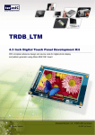
1 CONTENTS Chapter 1 About the Kit.................................................................................3 1.1 Kit Contents ....................................................................................................................................... 3 1.2 Connecting LTM to Altera DE Series Board........................................................................................ 3 1.3 Getting Help....................................................................................................................................... 6 Chapter 2 Architecture of the LTM ................................................................8 2.1 Features.............................................................................................................................................. 8 2.2 Block Diagram of the LTM................................................................................................................. 9 2.3 Pin Description of the 40-pin Interface of LTM................................................................................... 9 Chapter 3 Using the LTM .............................................................................12 3.1 The Serial Port Interface of the LCD Driver IC ................................................................................. 12 3.2 Input timing of the LCD panel display function ................................................................................ 14 3.3 The serial interface of the AD converter ............................................................................................ 17 Chapter 4 Digital Panel Design Demonstration ...........................................19 4.1 Demonstration Setup ........................................................................................................................ 19 4.2 Loading Photos into the Flash........................................................................................................... 19 4.3 Configuring the Ephoto Demonstration............................................................................................. 21 4.4 Block Diagram of the Ephoto Design................................................................................................ 24 4.5 Preprocessing the Desired Display Photo .......................................................................................... 25 4.6 Configuring the Pattern Generator for DE4/DE2-115/DE2/DE1 Board.............................................. 26 4.7 Configuring the Pattern Generator for DEN Board............................................................................ 29 4.8 Picture Viewer Demonstration .......................................................................................................... 30 4.9 LTM Starter Demonstration .............................................................................................................. 33 4.10 Video and Image Processing ........................................................................................................... 36 Chapter 5 Appendix .....................................................................................40 1 5.1 Absolute Maximum Ratings of the LCD Panel Module ..................................................................... 40 5.2 Power ON/OFF and Mode Change Sequence of the LCD Panel Module ........................................... 40 5.3 Register map of the LCD Driver IC .................................................................................................. 41 5.4 Register Definition of the LCD Driver IC ......................................................................................... 43 5.5 TV Revision History......................................................................................................................... 50 5.6 Always Visit LTM Webpage for New Applications............................................................................ 50 2 Chapter 1 About the Kit The TRDB_LTM (LTM) Kit provides everything you need to develop applications using a digital touch panel on an Altera DE4/DE2-115/DE2/DE1 board. The kit contains complete reference designs and source code for implementing a photo viewer demonstration and a color pattern generator using the LTM kit and an Altera DE2-115/DE2/DE1 board. This chapter provides users key information about the kit. 1.1 Kit Contents Figure 1.1 shows the picture of the TRDB_LTM package. The package includes: 1. The Terasic LCD Touch Panel Module (LTM) board 2. A 40-pin IDE cable 3. Complete reference design with source code Figure 1.1. The TRDB_LTM Package 1.2 Connecting LTM to Altera DE Series Board Please follow the two steps below to connect LTM to the Altera DE2-115/DE2/DE1 board: 3 1. Connect the IDE cable to the back of the LTM board, as shown in Figure 1.2 2. Connect the other end of the IDE cable to your DE4/DE2-115/DE2/DE1 board’s innermost expansion port (JP1) as shown in Figure 1.3 and Figure 1.6 Figure 1.2 Connect the IDE cable to the TRDB_LTM board Figure 1.2 Connect the IDE cable to the TRDB_LTM board Figure 1.3 Connect the other end of IDE cable to the DE2 board’s expansion port (innermost expansion port) 4 Figure 1.3 Connect the other end of IDE cable to the DE2 board’s expansion port (innermost expansion port) Figure 1.4 Connect the other end of IDE cable to the DE1 board’s expansion port (innermost expansion port) 5 Figure 1.5 Connect the other end of IDE cable to the DE2-115 board’s GPIO Figure 1.6 Connect the other end of IDE cable to the DE4 board’s expansion port (innermost expansion port) Figure 1.6 Connect the other end of IDE cable to the DE4 board’s expansion port (innermost expansion port) 1.3 Getting Help Here are some places to get help if you encounter any problem: Email to [email protected] Taiwan & China: +886-3-550-8800 6 Korea : +82-2-512-7661 Japan: +81-428-77-7000 7 Chapter 2 Architecture of the LTM This chapter will illustrate the architecture of the LTM including device features and block diagram. 2.1 Features The feature set of the LTM is listed below: 1. Equipped with Toppoly TD043MTEA1 active matrix color TFT LCD module. 2. Support 24-bit parallel RGB interface. 3. 3-wire register control for display and function selection. 4. Built-in contrast, brightness, and gamma modulation. 5. Converting the X/Y coordination of the touch point to its corresponding digital data via the Analog Devices AD7843 AD converter. 6. The general specifications of the LTM are listed below: Item Description Unit Display Size (Diagonal) 4.3 Inch Aspect ratio 15:9 - Display Type Transmissive - Active Area (HxV) 93.6 x 56.16 mm Number of Dots (HxV) 800 x RGB x480 dot Dot Pitch (HxV) 0.039 x 0.117 mm Color Arrangement Stripe - Color Numbers 16Million - 8 2.2 Block Diagram of the LTM The block diagram of the LTM is listed below: Figure 2.1 The block diagram of the LTM. The LTM consists of three major components: LCD touch panel module, AD converter, and 40-pin expansion header. All of the interfaces on the LTM are connected to Altera DE4/DE2-115/DE2/DE1 board via the 40-pin expansion connector. The LCD and touch panel module will take the control signals provided directly from FPGA as input and display images on the LCD panel. Finally, the AD converter will convert the coordinates of the touch point to its corresponding digital data and output to the FPGA via the expansion header. 2.3 Pin Description of the 40-pin Interface of LTM The pin description of the 40-pin connector follows: 9 Figure 2.2 The pin-out of the 40-pin connector. Pin Numbers Name Direction 1 2 ADC_PENIRQ_n ADC_DOUT output output ADC pen Interrupt ADC serial interface data out 3 ADC_BUSY output ADC serial interface busy 4 ADC_DIN input ADC serial interface data in 5 ADC_DCLK input ADC/LCD serial interface clock 6 B3 Input LCD blue data bus bit 3 7 B2 Input LCD blue data bus bit 2 8 B1 Input LCD blue data bus bit 1 9 B0 Input LCD blue data bus bit 0 10 NCLK Input LCD clock signal 11 NC N/A N/A 12 GND N/A Ground 13 DEN Input LCD RGB data enable 14 HD Input LCD Horizontal sync input 15 VD Input LCD Vertical sync input 16 B4 Input LCD blue data bus bit 4 17 B5 Input LCD blue data bus bit 5 18 B6 Input LCD blue data bus bit 6 19 B7 Input LCD blue data bus bit 7 20 G0 Input LCD green data bus bit 0 21 G1 Input LCD green data bus bit 1 22 G2 Input LCD green data bus bit 2 23 G3 Input LCD green data bus bit 3 24 G4 Input LCD green data bus bit 4 25 G5 Input LCD green data bus bit 5 26 G6 Input LCD green data bus bit 6 27 G7 Input LCD green data bus bit 7 10 Description 28 29 R0 VCC33 Input N/A LCD red data bus bit 0 Power 3.3V 30 GND N/A 31 R1 Input LCD red data bus bit 1 32 R2 Input LCD red data bus bit 2 33 R3 Input LCD red data bus bit 3 34 R4 Input LCD red data bus bit 4 35 R5 Input LCD red data bus bit 5 36 R6 Input LCD red data bus bit 6 37 R7 Input LCD red data bus bit 7 38 GREST Input Global reset, low active 39 SCEN Input LCD 3-wire serial interface enable/ADC chip enable 40 SDA Input/Output Ground LCD 3-wire serial interface data Table 2.1 The pin description of the 40-pin connector. 11 Chapter 3 Using the LTM This chapter illustrates how to use the LTM including how to control the serial port interface of the LCD driver IC and AD converter. Also, the timing requirement of the synchronous signal and RGB data which are outputted to the LCD panel module will be described. 3.1 The Serial Por t Interface of the LCD Driver IC The LCD and touch panel module on the LTM is equipped with a LCD driver IC to support three display resolutions and with functions of source driver, serial port interface, timing controller, and power supply circuits. To control these functions, users can use FPGA to configure the registers in the LCD driver IC via serial port interface. Also, there is an analog to digital converter (ADC) on the LTM to convert the analog X/Y coordinates of the touch point to digital data and output to FPGA through the serial port interface of the ADC. Both LCD driver IC and ADC serial port interfaces are connected to the FPGA via the 40-pin expansion header and IDE cable. Because of the limited number of I/O on the expansion header, the serial interfaces of the LCD driver IC and ADC need to share the same clock (ADC_DCLK) and chip enable (SCEN) signal I/O on the expansion header. To avoid both the serial port interfaces may interfere with each other when sharing the same clock and chip enable signals, the chip enable signal (CS), which is inputted into the ADC will come up with a logic inverter as shown in Figure 3.1. Users need to pay attention controlling the shared signals when designing the serial port interface controller. The detailed register maps of the LCD driver IC are listed in appendix chapter. The specifications of the serial port interface of the LCD driver IC are described below. 12 Figure 3.1 The serial interface of the LCD touch panel module and AD7843 The LCD driver IC supports a clock synchronous serial interface as the interface to a FPGA to enable instruction setting. Please notice that in addition to the serial port interface signals, NCLK input should also be provided while setting the registers. Figure 3.2 and Table 3.1 show the frame format and timing diagram of the serial port interface. The LCD driver IC recognizes the start of data transfer on the falling edge of SCEN input and starts data transfer. When setting instruction, the TPG110 inputs the setting values via SDA on the rising edge of input SCL. The first 6 bits (A5 ~ A0) specify the address of the register. The next bit means Read/Write command. “0” is write command. “1” is read command. Then, the next cycle is turn-round cycle. Finally, the last 8 bits are for Data setting (D7 ~ D0). The address and data are transferred from the MSB to LSB sequentially. The data is written to the register of assigned address when “End of transfer” is detected after the 16th SCL rising cycles. Data is not accepted if there are less or more than 16 cycles for one transaction Figure 3.2 The frame format and timing diagram of the serial port interface 13 Item Symbol Conditions Min. Max. Unit ts0 SCEN to SCL 150 ns ts1 SDA to SCL 150 ns th0 SCEN to SCL 150 ns th1 SDA to SCL 150 ns tw1L SCL pulse width 160 ns tw1H SCL pulse width 160 ns tw2 SCEN pulse width 1.0 ns SDA Setup Time SDA Hold Time Pulse Width Clock duty 40 60 % Table 3.1 The timing parameters of the serial port interface 3.2 Input timing of the LCD panel display function This section will describe the timing specification of the LCD synchronous signals and RGB data. To determine the sequencing and the timing of the image signals displayed on the LCD panel, the corresponding synchronous signals from FPGA to the LCD panel should follow the timing specification. Figure 3.3 illustrates the basic timing requirements for each row (horizontal) that is displayed on the LCD panel. An active-low pulse of specific duration (time t hpw in the figure) is applied to the horizontal synchronization (HD) input of the LCD panel, which signifies the end of one row of data and the start of the next. The data (RGB) inputs on the LCD panel are not valid for a time period called the hsync back porch ( t hbp ) after the hsync pulse occurs, which is followed by the display area ( t hd ). During the data display area the RGB data drives each pixel in turn across the row being displayed. Also, during the period of the data display area, the data enable signal (DEN) must be driven to logic high. Finally, there is a time period called the hsync front porch ( t hfp ) where the RGB signals are not valid again before the next hsync pulse can occur. The timing of the vertical synchronization (VD) is the same as shown in Figure 3.4, except that a vsync pulse signifies the end of one frame and the start of the next, and the data refers to the set of rows in the frame (horizontal timing). Table 3.2 and 3.3 show for different resolutions, the durations of time periods thpw, t hbp , t hd , and t hfp for both horizontal and vertical timing. Finally, the timing specification of the synchronous signals is shown in the Table 3.4. 14 Figure 3.3 LCD horizontal timing specification Panel Resolution Parameter Symbol NCLK Frequency FNCLK thd Horizontal valid data th 1 Horizontal Line Unit 800xRGBx480 480xRGBx272 400xRGBx240 33.2 9 8.3 MHz 800 480 400 NCLK 1056 525 528 NCLK Min. HSYNC Pulse Width Typ. 1 thpw Max. Hsync back porch Hsync front porch DEN Enable Time NCLK - thbp thfp tep 216 43 108 NCLK 40 2 20 NCLK 800 480 400 NCLK Table 3.2 LCD horizontal timing parameters 15 Figure 3.4 LCD vertical timing specification Panel Resolution Parameter Symbol tvd Vertical valid data tv Vertical period Unit 800xRGBx480 480xRGBx272 400xRGBx240 480 272 240 H 525 286 262 H Min. VSYNC Pulse Width Typ. 1 tvpw Max. Vertical back porch Vertical front porch Vertical blanking DEN Enable Time H - tvbp tvfp tvb TDEN 35 12 20 H 10 2 2 H 45 14 22 H 480 272 240 H Table 3.3 LCD vertical timing parameters 16 Parameter Symbol Min. Unit NCLK period PWCLK*1 25 ns NCLK pulse high period PWH*1 10 ns NCLK pulse low period PWL*1 10 ns HD,VD, DEN, data setup time tds 5 ns HD,VD, DEN, data hold time tdh 5 ns Table 3.4 The timing parameters of the LCD synchronous signals 3.3 The serial interface of the AD conver ter This section will describe how to obtain the X/Y coordinates of the touch point from the AD converter. The LTM also equipped with an Analog Devices AD7843 touch screen digitizer chip. The AD7843 is a 12-bit analog to digital converter (ADC) for digitizing x and y coordinates of touch points applied to the touch screen. The coordinates of the touch point stored in the AD7843 can be obtained by the serial port interface. To obtain the coordinate from the ADC, the first thing users need to do is monitor the interrupt signal ADC_PENIRQ_n outputted from the ADC. By connecting a pull high resistor, the ADC_PENIRQ_n output remains high normally. When the touch screen connected to the ADC is touched via a pen or finger, the ADC_PENIRQ_n output goes low, initiating an interrupt to a FPGA that can then instruct a control word to be written to the ADC via the serial port interface. The control word provided to the ADC via the DIN pin is shown in Table 3.5. This provides the conversion start, channel addressing, ADC conversion resolution, configuration, and power-down of the ADC. The detailed information on the order and description of these control bits can be found from the datasheet of the ADC in the DATASHEET folder on the LTM System CD-ROM. MSB LSB S A2 Bit Mnemonic A1 A0 MODE S ER / D EF PD1 PD0 Comment Start Bit. The control word starts with the first high bit on DIN. A 7 S new control word can start every 15th DCLK cycle when in the 12-bit conversion mode, or every 11th DCLK cycle when in 8-bit conversion mode. Channel Select Bits. These three address bits, along with the 6-4 A2-A0 S ER / D EF bit, control the setting of the multiplexer input, switches, and reference inputs. 17 12-Bit/8-Bit Conversion Select Bit. This bit controls the resolution 3 MODE of the following conversion. With 0 in this bit, the conversion has a 12-bit resolution, or with 1 in this bit, the conversion has a 8-bit resolution. Single-Ended/Differential Reference Select Bit. Along with Bits A2 2 1,0 SER / DEF PD1,PD0 –A0, this bit controls the setting of the multiplexer input, switches, and reference inputs. Power Management Bits. These two bits decode the power-down mode of the AD7843. Table 3.5 Control register bit function description Figure 3.5 shows the typical operation of the serial interface of the ADC. The serial clock provides the conversion clock and also controls the transfer of information to and from the ADC. One complete conversion can be achieved with 24 ADC_DCLK cycles. The detailed behavior of the serial port interface can be found in the datasheet of the ADC. Note that the clock (ADC_DCLK) and chip enable signals (SCEN) of the serial port interface SHRAE the same signal I/O with LCD driver IC. Users should avoid controlling the LCD driver IC and ADC at the same time when designing the serial port interface controller. Also, because the chip enable signal (SCEN) inputted to the ADC comes up with a logic inverter, the logic level of the SCEN should be inverse when it is used to control the ADC. Figure 3.5 Conversion timing of the serial port interface 18 Chapter 4 Digital Panel Design Demonstration This chapter illustrates how to exercise the LTM reference design provided with the kit. Users can follow the instructions in this chapter to build a 4.3 inch Ephoto demonstration and pattern generator using the DE2-115/DE2/DE1/DEN in 10 minutes. 4.1 Demonstration Setup The demonstration configuration is illustrated as Figure 4.1. Display the bmp format photos, which are saved into the flash of DE2-115/DE2/DE1, on LTM module, through the control of FPGA on DE2-115/DE2/DE1 board. Users can change the displayed photo by touching the LTM touch panel. Figure 4.1. The Ephoto demonstration configuration setup 4.2 Loading Photos into the Flash Locate the project directory from the CD-ROM and follow the steps below: A: For Altera DE2-115 Board 19 Quartus II Project Directory: DE2_115_Control_Panel FPGA Bitstream Used: DE2_115_ControlPanel.sof B: For Altera DE2 Board Quartus II Project Directory: DE2_Control_Panel_V1.04 FPGA Bitstream Used: DE2_USB_API.sof or DE2_USB_API.pof C: For Altera DE1 Board Quartus II Project Directory: DE1_Control_Panel_V1.00 FPGA Bitstream Used: DE1_USB_API.sof or DE1_USB_API.pof 1. Make sure the USB-Blaster download cable is connected into the host PC 2. Load the Control Panel bit stream (DE2_USB_API/ DE1_USB_API) into the FPGA. Please also refer to Chapter 3 DE2/DE1 Control Panel in the Altera DE2/DE1 User Manual for more details in the Control Panel Software Figure 4.2. Programming window 3. Execute the Control Panel application software 4. Open the USB port by clicking Open > Open USB Port 0. The DE2/DE1 Control Panel application will list all the USB ports that connect to DE2/DE1 board 5. Switch to FLASH page and click on the “Chip Erase(40 Sec)” bottom to erase Flash data 20 Figure 4.3. DE2 control panel window 6. Click on the “File Length” checkbox to indicate that you want to load the entire file 7. Click on the “Write a File to FLASH” bottom. When the Control Panel responds with the standard Windows dialog box and asks for the source file, select the “480x3.bmp” file in the “Photo” directory 4.3 Configuring the Ephoto Demonstration Locate the project directory from the CD-ROM and follow the steps below: A: For Altera DE2-115 Board Quartus II Project Directory: DE2_115_LTM_Ephoto FPGA Bitstream Used: DE2_115_LTM_Ephoto.sof or DE2_115_LTM_Ephoto.pof B: For Altera DE2 Board Quartus II Project Directory: DE2_LTM_Ephoto FPGA Bitstream Used: DE2_LTM_Ephoto.sof or DE2_LTM_Ephoto.pof C: For Altera DE1 Board Quartus II Project Directory: DE1_LTM_Ephoto FPGA Bitstream Used: DE1_LTM_Ephoto.sof or DE1_LTM_Ephoto.pof 21 1.Ensure the connection is made correctly as shown in Figure 4.4 and Figure 4.7. Make sure the IDE cable is connected to JP1 of the DE-115/DE2/DE1 board 2.Download the bitstream (DE2_115_LTM_Ephoto /DE2_LTM_Ephoto/ DE1_LTM_Ephoto) to the DE2/DE1 board 3.As shown in Figurate 4.5, touch the bottom left corner and top right corner of the LTM touch panel to display the next and previous photos respectively Figure 4.4. The connection setup for the Ephoto demonstration with DE2-115 board Figure 4.5. The connection setup for the Ephoto demonstration with DE2 board 22 Figure 4.6. The connection setup for the Ephoto demonstration with DE1 board Touch here for the previous photo Touch here for the next photo Figure 4.7. The touch function of changing displayed photo 23 4.When users touch the LTM screen, the 7-segment displays "HEX6~HEX4" and "HEX2~HEX0" on the DE2 board will display the X and Y coordinates (in Hexadecimal format) of the touch point respectively (DE2-115/DE2 board only). Figure 4.8 indicates that the x and y coordinates of the corners on the LTM touch screen Figure 4.8. The x and y coordinates of the corners on the LTM touch screen 4.4 Block Diagram of the Ephoto Design This section will describe the block diagram of the Ephoto demonstration to help users in reading the code provided. Figure 4.9 shows the block diagram of the EPhoto demonstration. As soon as the bit stream is downloaded into the FPGA, the register values of the LCD driver IC using to control the LCD display function will be configured by the LCD_SPI_Controller block, which uses the serial port interface to communicate with the LCD driver IC. Meanwhile, the Flash_to_SDRAM_Controller block will read the RGB data of one picture stored in the Flash, and then write the data into SDRAM buffer. Accordingly, both the synchronous control signals and the picture data stored in the SDRAM buffer will be sent to the LTM via the LCD_Timing_Controller block. When users touch LTM screens, the x and y coordinates of the touch point will be obtained by the ADC_SPI_Controller block through the ADC serial port interface. Then the Touch_Point_Detector block will determine whether these coordinates are in a specific range. If the coordinates fit the range, the Touch_Point_Detector block will control the Flash_to_SDRAM_Controller block to read the next or previous picture's data from the Flash and repeat the steps as mentioned before to command the LTM to display the next or previous picture. 24 Figure 4.9. The block diagram of the Ephoto demonstration 4.5 Preprocessing the Desired Display Photo If users want to display their own photos on the LTM ,they can follow the steps below: 1. Prepar three 24 bit bmp format photos and image resolution should be 800(high) x 480(width), as shown in Figure 4.10 Figure 4.10. Original photo‘s resolution format 2. Use the image processing software (such as Photoshop or Photoimpact) to rotate the images counterclockwise and then merge these photos into a new photo image. The new photo‘s image resolution should be 1440(high) x 800 (width), as shown in Figure 4.11 25 Figure 4.11 The photo format of the DE2_LTM_Ephoto/ DE1_LTM_Ephoto demonstration 4.6 Configuring the Patter n Generator for DE4/DE2-115/D E2/DE1 Board Locate the project directory from the CD-ROM and follow the steps below: A: For Altera DE4 Board Quartus II Project Directory: DE4_LTM_Test FPGA Bitstream Used: DE4_LTM_Test.sof or DE4_LTM_Test.pof 26 B: For Altera DE2-115 Board Quartus II Project Directory: DE2_115_LTM_Test FPGA Bitstream Used: DE2_115_LTM_Test.sof or DE2_115_LTM_Test.pof C: For Altera DE2 Board Quartus II Project Directory: DE2_LTM_Test FPGA Bitstream Used: DE2_LTM_Test.sof or DE2_LTM_Test.pof D: For Altera DE1 Board Quartus II Project Directory: DE1_LTM_Test FPGA Bitstream Used: DE1_LTM_Test.sof or DE1_LTM_Test.pof 1. Ensure the connection is made correctly as shown in Figure 4.12 and Figure 4.15 Make sure the IDE cable is connected to JP1 of the DE4/DE2-115/DE2/DE1 board Figure 4.12. The connection setup for the pattern generator demo with DE4 board 27 Figure 4.13. The connection setup for the pattern generator demo with DE2-115 board Figure 4.14. The connection setup for the pattern generator demo with DE2 board 28 Figure 4.15. The connection setup for the pattern generator demo with DE1 board 2. Download the bitstream (DE2_115_LTM_Test/DE2_LTM_Test/ DE1_LTM_Test) to the DE2-115/DE2/DE1 board 3. Press KEY0 on the DE2-115/DE2/DE1 board to reset the circuit 4. Touch the LTM screen to switch to the other Pattern 5. The following table summarizes the Pattern type of this demonstration Pattern Gray bar Color bar 50% gray level pattern White pattern 6. When you touch the LTM panel, the 7-segment displays “HEX6~HEX4” and “HEX2~HEX0” on the DE2-115/DE2 will display the X and Y coordinates (in Hexadecimal format) of the LTM panel respectively (DE2-115/DE2 board only) 4.7 Configuring the Patter n Generator for DEN Board Locate the project directory from the CD-ROM and follow the steps below: 29 Quartus II Project Directory: DEN_LTM_Test FPGA Bitstream Used: DEN_LTM_Test.pof 1. Ensure the connection is made correctly as shown in Figure 4.16. Make sure the IDE cable is connected to the extension header of the DEN board Figure 4.16. The connection setup for the pattern generator demo with DEN board 2. 3. 4. 5. Download the bitstream (DEN_LTM_Test.pof) to the DEN board Press BUTTON1 on the DEN board to reset the circuit Touch the LTM screen to switch to the other Pattern The following table summarizes the Pattern type of this demonstration Pattern Gray bar Color bar 50% gray level pattern White pattern 4.8 Picture Viewer Demonstration This demonstration shows a simple picture viewer implementation using Nios II based SOPC system. It first read JPEG image from SD Card and then decode it using the Nios II. The frame buffers will be filled with decoded raw image data. The LTM will show the image that the buffer being displayed point to. When users touch the LTM, it will proceed to display the next buffered 30 image until there is no filled buffer. Figure 4.17 shows the block diagram of this demonstration. Figure 4.17. Block diagram of the picture viewer demonstration Demonstration Setup, File Locations, and Instructions Project directory: DE2_115_LTM_Pic Bit stream used: DE2_115_LTM_Pic.sof Nios II Workspace: DE2_115_LTM_Pic\Software Format your SD Card into FAT16 format Place the jpg image files to the \jpg subdirectory of the SD Card. For best display result, the image should have a resolution of 800x480 or the multiple of that Connect the LTM to the DE2-115 board, insert the SD Card to the SD Card slot on the DE2-115, as shown in Figure 4.18 Load the bitstream into the FPGA on the DE2-115 board Run the Nios II Software under the workspace DE2_115_LTM_Pic\Software Touch the play button will proceed to display the next image, as shown in Figure 4.19 When there is no filled up frame buffers for display, it will enter into Loading mode. The top left corner will print information about the loading progress. In the Loading mode, program won’t response to users’ touch action. Table4.1 shows the instructions for running the demonstration 31 Figure 4.18 Picture viewer demonstration setup Table 4.1 Touch panel displayed information Display information Implication Press the play button to display the next buffered image Indicates the loading progress Figure 4.19 Picture viewer demonstration runtime screen shot 32 4.9 LTM Star ter Demonstration The LTM starter demonstration takes user the initial experience of an embedded system integrating a LCD Touch Panel. This demonstration consists of four sub item, Picture, Touch, Paint and Color pattern generator. The Picture program reads BMP images from SD Card and displays them on the LCD Touch Panel. As a response of your tap on the Touch Screen, it will display the next BMP image. The Touch segment draws a circle on where you touch the screen and updates its coordinates on the top left corner. The Paint segment is a little interesting. Your finger or touch pen slides on the Touch Panel. The software responds to every collected single touch and draws solid dots on the LCD Touch Panel. The formed curves represent your touch traces. There is also a color palette on the bottom side of the LCD, from where you could get your painting color. For best user-experience, you may need a touch pen. The pattern generator can be treated as an upgrade version of the LCD test program. The software successively generates different color patterns after a fixed time delay. Users could use it to quickly investigate any flaw of the LCD. Figure 4.20 shows the hardware system block diagram of this demonstration. The system is clocked by an external 50MHz Oscillator. Through the internal PLL module, the generated 100MHz clock is used for Nios II processor and other components, and there also a 40MHz pixel clock for the video pipeline and 10MHz for low-speed peripherals. The Nios II CPU runs the application software and controls all the peripherals. A scatter-gather DMA is used to transfer pixel data from the video buffer to the video pipeline. Figure 4.20 Block diagram of the LTM Starter demonstration 33 Figure 4.21 illustrates the software structure of this demonstration. The Nios II PIO block provides basic I/O functions to directly access the hardware. The SD Card block implements 4-bit mode protocol for communication with the SD Cards. The FAT File System block implements reading function for FAT16 and FAT32 file system. The touch panel SPI HAL block handles the bottom hardware responding and interface to upper layers. The sgdma HAL allocates required frame/descriptor buffers to specified memory address and is responsible of handling frame buffer update issue. Figure 4.21. Software stack of the LTM Starter demonstration Demonstration Source Code Project directory: DE2_115_LTM_Starter Bit stream used: DE2_115_LTM_Starter.sof Nios II Workspace: DE2_115_LTM _Starter\Software Demonstration Batch File Demo Batch File Folder: DE2_115_LTM _Starter \demo_batch The demo batch file includes the following files: Batch File: DE2_115_LTM _Starter.bat, DE2_115_LTM _Starter_bashrc FPGA Configure File: DE2_115_LTM _Starter.sof Nios II Program: DE2_115_LTM _Starter.elf Demonstration Setup Make sure Quartus II and Nios II are installed on your PC Power on the DE2-115 board Connect USB Blaster to the DE2-115 board and install USB Blaster driver if necessary Copy some bmp images to the root directory of the SD Card 34 Insert the SD Card into the SD Card socket of LTM Execute the demo batch file “DE2_115_LTM _Starter.bat” under the batch file folder, DE2_115_LTM _Starter\demo_batch After Nios II program is downloaded and executed successfully, a prompt message will be displayed in nios2-terminal From on the touch panel, tap any icon of the main interface and start the experience Under each sub item, touch the Exit button on the left bottom corner will lead you back to the main interface. Figure4.22 and 4.23 give photos of sub items when running the DE2-115 LTM Starter demonstration Figure 4.22 Touch sub item of the DE2-115 LTM Starter demonstration 35 Figure 4.23 Color pattern sub item of DE2-115 LTM Starter demonstration 4.10 Video and Image Processing The Video and Image Processing (VIP) Example Design demonstrates dynamic scaling and clipping of a standard definition video stream in either National Television System Committee (NTSC) or phase alternation line (PAL) format and picture-in-picture mixing with a background layer. The video stream is output in high definition resolution (800×480) on LTM The example design demonstrates a framework for rapid development of video and image processing systems using the parameterizable MegaCore® functions that are available in the Video and Image Processing Suite. Available functions are listed in Table 4.2. Table 4.2 VIP IP cores functions IP MegaCore Function Frame Reader Control Synchronizer Switch Color Space Converter Chroma Resampler 2D FIR Filter Description Reads video from external memory and outputs it as a stream. Synchronizes the changes made to the video stream in real time between two functions. Allows video streams to be switched in real time. Converts image data between a variety of different color spaces such as RGB to YCrCb. Changes the sampling rate of the chroma data for image frames, for example from 4:2:2 to 4:4:4 or 4:2:2 to 4:2:0. Implements a 3 x 3, 5 x 5, or 7 x 7 finite impulse response (FIR) filter on an image data stream to smooth or sharpen images. 36 Alpha Blending Mixer Scaler Deinterlacer Test Pattern Generator Clipper Color Plane Sequencer Frame Buffer 2D Median Filter Gamma Corrector Clocked Video Input/Output Mixes and blends multiple image streams—useful for implementing text overlay and picture-in-picture mixing. A sophisticated polyphase scaler that allows custom scaling and real-time updates of both the image sizes and the scaling coefficients. Converts interlaced video formats to progressive video format using a motion adaptive deinterlacing algorithm. Also supports 'bob' and "weave" algorithms Generates a video stream that contains still color bars for use as a test pattern. Provides a way to clip video streams and can be configured at compile time or at run time. Changes how color plane samples are transmitted across the Avalon-ST interface. This function can be used to split and join video streams, giving control over the routing of color plane samples. Buffers video frames into external RAM. This core supports double or triple-buffering with a range of options for frame dropping and repeating. Provides a way to apply 3 x 3, 5 x 5, or 7 x 7 pixel median filters to video images. Allows video streams to be corrected for the physical properties of display devices. These two cores convert the industry-standard clocked video format (BT-656) to Avalon-ST video and vice versa. These functions allow you to fully integrate common video functions with video interfaces, processors, and external memory controllers. The example design uses an Altera Cyclone® IV E EP4CE115F29 featured DE2-115 board. A video source is input through an analog composite port on DE2-115 which generates a digital output in ITU BT656 format. A number of common video functions are performed on this input stream in the FPGA. These functions include clipping, chroma resampling, motion adaptive deinterlacing, color space conversion, picture-in-picture mixing, and polyphase scaling. The input and output video interfaces on the DE2-115 are configured and initialized by software running on a Nios® II processor. Nios II software demonstrates how to control the clocked video input, clocked video output, and mixer functions at run-time is also provided. The video system is implemented using the SOPC Builder system level design tool. This abstracted design tool provides an easy path to system integration of the video processing data path with a NTSC or PAL video input, VGA output, Nios II processor for configuration and control. The Video and Image Processing Suite MegaCore functions have common open Avalon-ST data interfaces and Avalon Memory-Mapped (Avalon-MM) control interfaces to facilitate connection of a chain of video functions and video system modeling. In addition, video data is transmitted between the Video and Image Processing Suite functions using the Avalon-ST Video protocol, which facilitates building run-time controllable systems and error recovery. Figure 4.24 shows the Video and Image Processing block diagram. 37 Figure 4.24 VIP Example SOPC Block Diagram (Key Components) Demonstration Setup, File Locations, and Instructions Project directory: DE2_115_LTM_VIP Bit stream used: DE2_115_LTM_VIP.sof Connect a DVD player’s composite video output(yellow plug) to the Video-IN RCA jack(J12) of the DE2-115 board. The DVD player has to be configured to provide NTSC output or PAL output Connect the VGA output of the DE2-115 board to a VGA monitor (both LCD and CRT type of monitors should work) Connect LTM to the GPIO port of DE2-115 Load the bit stream into FPGA (note*) Run the Nios II and choose DE2_115_LTM_VIP \software as the workspace. Click on the Run button (note *) Press and drag the video frame box will result in scaling the playing window to any size. Figure 4.25 gives a photograph of the running result of the demonstration Note: execute DE2_115_LTM_VIP \demo_batch\VIP.bat will download .sof and .elf files. 38 Figure 4.25 Running result of the DE2-115 LTM VIP demonstration 39 Chapter 5 Appendix This chapter describes in more detail about the characteristic of the LCD for Hardware/Software developer’s convenience. 5.1 Absolute Maximum Ratings of the LCD Panel Module Item Symbol Min Max Unit Logic Power Supply Voltage VCC 2.7 3.6 V Input Signal Voltage VIN1 0 VCC V Remark VD, HD, NCLK, SDA,SCL, SCEN,DEN,GREST Back Light Forward Current Operating Temperature Storage Temperature IF 18 23 TOPR -20 +70 C +85 C TSTG -40 mA 5.2 Power ON/OFF and Mode Change Sequence of the L CD Panel Module Power on (low power or reset mode to normal mode) sequence: 40 Power off (normal mode to low power mode) sequence : 5.3 Re gister map of the LCD Driver IC Address Default Read/Write 0x00 0x00 R/W 0x01 0xC1 R 0x02 0x07 R/W 0x03 0x5F R/W Description [7:0]:Testing register [7:4]:Chip ID [3:0]: Chip version [7:6]: Dot inversion method selection [5]: VD polarity [4]: HD polarity [3]: Input clock latch data edge [2:0]: Resolution selection [7]: Hardware or software selection for resolution and standby. [6]:Pre-charge on/off [5:4]: Output driving capability [3]: PWM output on/off [2]: VGL pump output on/off 41 [1]: CP_CLK output on/off[0]: Power management 0x04 0x17 R/W [5:4]: VGL pump frequency [3:2]: CP_CLK frequency [1]: Vertical reverse mode [0]: Horizontal reverse mode 0x05 0x20 R/W [5:0]: Horizontal start position for Sync mode 0x06 0x08 R/W [3:0]: Vertical start position for Sync mode 0x07 0x20 R/W [5:0]: CKH high pulse width 0x08 0x20 R/W [5:0]: CKH non-overlap 0x09 0x20 R/W [5:0]: ENB rising to CKH non-overlap 0x0A 0x20 R/W [5:0]: ENB low pulse width 0x0B 0x20 R/W [5:0]: R gain of contrast 0x0C 0x20 R/W [5:0]: G gain of contrast 0x0D 0x20 R/W [5:0]: B gain of contrast 0x0E 0x10 R/W [5:0]: Offset of brightness R 0x0F 0x10 R/W [5:0]: Offset of brightness G 0x10 0x10 R/W [5:0]: Offset of brightness B 0x11 0x00 R/W [7:6]: GAMMA 0[9:8] of gamma Correction [5:4]: GAMMA 8[9:8] of gamma Correction [3:2]: GAMMA 16[9:8] of gamma Correction [1:0]: GAMMA 32[9:8] of gamma Correction [7:6]: GAMMA 64[9:8] of gamma Correction [5:4]: GAMMA 96[9:8] of gamma Correction 0x12 0x5B R/W [3:2]: GAMMA 128[9:8] of gamma Correction [1:0]: GAMMA 192[9:8] of gamma Correction [7:6]: GAMMA 224[9:8] of gamma Correction [5:4]: GAMMA 240[9:8] of gamma 0x13 0xFF R/W Correction [3:2]: GAMMA 248[9:8] of gamma Correction [1:0]: GAMMA 256[9:8] of gamma Correction 0x14 0X00 R/W [7:0]: GAMMA 0[7:0] of gamma Correction 0x15 0X20 R/W [7:0]: GAMMA 8[7:0] of gamma Correction 0X16 0X40 R/W [7:0]: GAMMA 16[7:0] of gamma Correction 0X17 0X80 R/W [7:0]: GAMMA 32[7:0] of gamma Correction 0X18 0x00 R/W [7:0]: GAMMA 64[7:0] of gamma Correction 0X19 0X80 R/W [7:0]: GAMMA 96[7:0] of gamma Correction 0x1A 0x00 R/W [7:0]: GAMMA 128[7:0] of gamma Correction 0x1B 0x00 R/W [7:0]: GAMMA 192[7:0] of gamma Correction 0x1C 0X80 R/W [7:0]: GAMMA 224[7:0] of gamma Correction 0x1D 0XC0 R/W [7:0]: GAMMA 240[7:0] of gamma Correction 0x1E 0XE0 R/W [7:0]: GAMMA 248[7:0] of gamma Correction 0x1F 0XFF R/W [7:0]: GAMMA 256[7:0] of gamma Correction 0x20 0xD2 R/W [7:4]: Positive gamma output voltage level for source driver input FFH [3:0]: Positive gamma output voltage level for source driver input 00H 0X21 0xD2 R/W [7:4]: Negative gamma output voltage level for source driver input FFH [3:0]: Negative gamma output voltage level for source driver input 00H 0X22 0x05 R/W [3:0]: DC VCOM level 42 5.4 Re gister Definition of the LCD Driver IC R02h: R02[7:6]: Dot inversion method selection R02[7:6] Function Note Default (initial setting value) 0 0 Type1 0 1 Type2 1 0 Type3 1 1 Setting prohibited(Type1) R02[5]: VD polarity R02[5] Function Note 0 Low pulse Default (initial setting value) 1 High pulse R02[4]: HD polarity R02[4] Function Note 0 Low pulse Default (initial setting value) 1 High pulse R02[3]: Input clock latch data edge R02[5] Function Note 0 Latch data at NCLK falling edge Default (initial setting value) 1 Latch data at NCLK rising edge R02[2:0]: Resolution selection R02[2:0] Input Sequence Output Resolution Note 0 0 0 400RGBx240 800RGBx480 (Dual Scan) 0 0 1 480RGBx272 800RGBx480 (Dual Scan) 0 1 0 Setting Prohibited 0 1 1 Setting Prohibited 1 0 0 Setting Prohibited 1 0 1 1 1 0 1 1 1 480RGBx272 480RGBx272 Setting Prohibited 800RGBx480 800RGBx480 43 Default R03h: R03[7]: Hardware or Software selection for resolution and standby R03[7] Function Note 0 Hardware pin (RS[3:1,STBY]) Default (initial setting value) 1 Software register(R02[2:0,R03[0]) R03[6]: Pre-charge ON/OFF R03[6] Function Note 0 Pre-charge disable 1 Pre-charge enable Default (initial setting value) Function Note R03[5:4]: Driving capability R03[5:4] 0 0 75% 0 1 100% 1 0 150% 1 1 200% Default (initial setting value) R03[3]: PWM output ON/OFF R03[3] Function 0 PWM disable 1 PWM enable Note Default (initial setting value) R03[2]: VGL pump output ON/OFF R03[2] Function Note 0 VGL pump disable 1 VGL pump enable Default (initial setting value) Function Note R03[1]: CP_CLK output ON/OFF R03[1] 0 CP_CLK disable 1 CP_CLK enable Default (initial setting value) Function Note Power management R03[0] 44 0 Standby mode 1 Normal operation Default (initial setting value) Note: In standby mode, DOUT [400:1], when VCOM are connected to GND, PWM disabled. Control signals STV, CKV, CKH1~CKH6, and XENB are low, while XCKV, XCKH1~XCKH6, and ENB are high. CP_CLK1 is pulled high and CP_CLK is pulled low R04h: R04[5:4]: VGL pump frequency R04[5:4] Period(Frequency for WVGA) 0 0 2 * H(~16KHz) 0 1 1 * H(~32KHz) 1 0 1/2 * H(~64KHz) 1 1 1/4 * H(~128KHz) Note Default (initial setting value) R04[3:2]: CP_CLK frequency R04[5:4] Period(Frequency for WVGA) 0 0 2 * H(~16KHz) 0 1 1 * H(~32KHz) 1 0 1/2 * H(~64KHz) 1 1 1/4 * H(~128KHz) Note Default (initial setting value) R04[1]: Vertical reverse function R04[1] Function Note 0 Reverse (CSV=L) 1 Normal (CSV=H) Default (initial setting value) R04[0]: Horizontal reverse function R04[0] Function 0 Reverse 1 Normal Note Default (initial setting value) R05h: R05[5:0]: Horizontal display position shift for SYNC mode R05[5:0] 0 0 0 0 Function 0 0 -32 NCLK 45 Note 0 0 0 0 0 1 -31 NCLK : : : : : : : 0 1 1 1 1 0 -2 NCLK 0 1 1 1 1 1 -1 NCLK 1 0 0 0 0 0 Center 1 0 0 0 0 1 +1 NCLK 1 0 0 0 1 0 +2 NCLK : : : : : : : 1 1 1 1 1 0 +30 NCLK 1 1 1 1 1 1 +31 NCLK (display shift right) Default (initial setting value) (display shift left) R06h: R06[3:0]: Vertical display position shift for SYNC mode R06[3:0] Function 0 0 0 0 -8 NCLK 0 0 0 1 -7 NCLK : : : : : 0 1 1 0 -2 NCLK 0 1 1 1 -1 NCLK 1 0 0 0 Center 1 0 0 1 +1 NCLK 1 0 1 0 +2 NCLK : : : : : 1 1 1 0 +6 NCLK 1 1 1 1 +7 NCLK Note (display shift down) Default (initial setting value) (display shift up) R07h~R0Ah: R07[5:0]: CKH high pulse width adjustment. Set 0x20 for normal operation. R08[5:0]: CKH non-overlap adjustment. Set 0x20 for normal operation (around 0.6us). R09[5:0]: ENB to CKH1 non-overlap adjustment. Set 0x20 for normal operation (around 1.2us). R0A[5:0]: ENB low pulse width adjustment. Set 0x20 for normal operation (around 2.8us). 46 Notice that CKV transition timing is in the middle of ENB low pulse. R07~R0A[5:0] Function 0 0 0 0 0 0 -32 NCLK 0 0 0 0 0 1 -31 NCLK : : : : : : : 0 1 1 1 1 0 -2 NCLK 0 1 1 1 1 1 -1 NCLK 1 0 0 0 0 0 Center 1 0 0 0 0 1 +1 NCLK 1 0 0 0 1 0 +2 NCLK : : : : : : : 1 1 1 1 1 0 +30 NCLK 1 1 1 1 1 1 +31 NCLK Note Default (initial setting value) R0Bh: R0B[5:0]: R Gain of Contrast R0B[5:0] R Gain of Contrast 0x00 0.00000 0x20 1.00000 0x3F 1.96875 Note Default (initial setting value) R0Ch: R0C[5:0]: G Gain of Contrast R0C[5:0] G Gain of Contrast 0x00 0.00000 0x20 1.00000 0x3F 1.96875 Note Default (initial setting value) R0Eh: R0E[5:0]: R Offset of Brightness R0E[5:0] R Offset of Brightness 0x00 -16 0x10 0 0x3F 47 R0Fh: 47 Note Default (initial setting value) R0F[5:0]: G Offset of Brightness R0F[5:0] G Offset of Brightness 0x00 -16 0x10 0 0x3F 47 Note Default (initial setting value) R10h: R10[5:0]: B Offset of Brightness R10[5:0] B Offset of Brightness 0x00 -16 0x10 0 0x3F 47 Note Default (initial setting value) R11h ~ R1Fh: Gamma Correction The gamma correction is done by 11-segment piecewise linear interpolation. The 11 segments are defined with 12 register values for level 0, 8, 16, 32, 64, 96,128, 192, 224, 240, 248, and 256 for positive polarity. Negative polarity data are generated symmetrically. The gamma correction output is then fed to 8-bit DAC and OP to drive the source lines on the panel. R20h : Voltage range for positive polarity (when VDDP=5V and VDDN=-5V) 48 R20[7:4] defines positive polarity DAC reference voltage for code FFH 0xD R20[7:4] Gamma 0x0 0x1 0x2 0x3 0x4 0x5 0x6 0x7 0x8 0x9 0xA 0xB 0xC 3.3 3.4 3.5 3.6 3.7 3.8 3.9 4 4.1 4.2 4.3 4.4 4.5 (Default) 4.6 0xE 0xF 4.7 4.8 Level R20[3:0] defines positive polarity DAC reference voltage for code 00H 0x2 R20[3:0] Gamma 0x0 0x1 0.2 0.25 (Default) 0.3 0x3 0x4 0x5 0x6 0x7 0x8 0x9 0xA 0xB 0xC 0xD 0xE 0xF 0.35 0.4 0.45 0.5 0.55 0.6 0.65 0.7 0.75 0.8 0.85 0.9 0.95 0xE 0xF -4.7 -4.8 Level R21 : Voltage range for negative polarity (when VDDP=5V and VDDN=-5V) R21[7:4] defines negative polarity DAC reference voltage for code FFH 0xD R21[7:4] Gamma 0x0 0x1 0x2 0x3 0x4 0x5 0x6 0x7 0x8 0x9 0xA 0xB 0xC -3.3 -3.4 -3.5 -3.6 -3.7 -3.8 -3.9 -4 -4.1 -4.2 -4.3 -4.3 -4.5 (Default) -4.6 Level R21[3:0] defines negative polarity DAC reference voltage for code 00H R21[3:0] 0x0 0x1 0x2 0x3 0x4 0x5 0x6 0x7 0x8 0x9 0xA 0xB 0xC 0xD 0xE 0xF -0.35 -0.4 -0.45 -0.5 -0.55 -0.6 -0.65 -0.7 -0.75 -0.8 -0.85 -0.9 -0.95 0x6 0x7 0x8 0x9 0xA 0xB 0xC 0xD 0xE 0xF -0.1 -0.2 -0.3 -0.4 -0.5 -0.6 -0.7 -0.8 -0.9 -1 (Default) Gamma -0.2 -0.25 -0.3 Level R22 : DC VCOM level R22[3:0] defines DC VCOM level 0x5 R22[3:0] VCOM 0x0 0x1 0x2 0x3 0x4 0.5 0.4 0.3 0.2 0.1 (Default) 0 Level 49 5.5 TV Revision Histor y Version Change Log V1.0 Initial Version (Preliminary) V1.1 Edit appendix. V1.2 Edit Ch3 and Ch4. V1.2.1 Edit Figure 4.1, Figure 4.11, Figure 4.12, and Figure 4.13 V1.2.2 Edit chapter contents. V1.2.3 Modify Table 2.1 and Figure 3.1 V1.2.4 Picture viewer, Starter, VIP section added DE2-115/DE4 related information added 5.6 Always Visit LTM Webpage for New Applications We will continually provide interesting examples and labs on our LTM webpage. Please visit www.altera.com or ltm.terasic.com for more information. 50