1
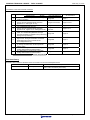
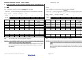
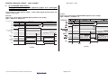
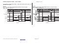
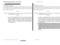
Date: May. 21, 2014 RENESAS TECHNICAL UPDATE 1753, Shimonumabe, Nakahara-ku, Kawasaki-shi, Kanagawa 211-8668 Japan Renesas Electronics Corporation Product Category Title MPU/MCU Document No. TN-RL*-A026A/E Correction for Incorrect Description Notice RL78/G13 Descriptions in the Hardware User’s Manual Rev. 3.10 Changed Information Category Technical Notification Reference Document RL78/G13 User’s Manual: Hardware Rev.3.10 R01UH0146EJ0310 (Nov. 2013) Rev. 1.00 Lot No. Applicable Product RL78/G13 R5F100xxx, R5F101xxx All lots This document describes misstatements found in the RL78/G13 User’s Manual: Hardware Rev.3.10 (R01UH0146EJ0310). Corrections Applicable Item 5.3.9 High-speed on-chip oscillator trimming register (HIOTRM) 12.5.7 SNOOZE mode function Timing Chart of SNOOZE Mode Operation (Figure 12-71. and Figure 12-73.) 12.6.3 SNOOZE mode function 12.6.3 SNOOZE mode function Timing Chart of SNOOZE Mode Operation (Figure 12-90., Figure 12-91. and Figure 12-93.) 16.4.3 Multiple interrupt servicing Table 16-5. Relationship Between Interrupt Requests Enabled for Multiple Interrupt Servicing During Interrupt Servicing 20.2 Configuration of Power-on-reset Circuit Figure 20-2. Timing of Generation of Internal Reset Signal by Power-on-reset Circuit and Voltage Detector (1) 29.5.1 Serial array unit (1) During communication at same potential (UART mode) 29.7 Data Memory STOP Mode Low Supply Voltage Data Retention Characteristics 30.7 Data Memory STOP Mode Low Supply Voltage Data Retention Characteristics Applicable Page Contents Page 243 Incorrect descriptions revised Pages 579 and 581 Incorrect descriptions revised Page 606 Incorrect descriptions revised Pages 608, 609 and 611 Incorrect descriptions revised Page 796 Incorrect descriptions revised Page 829 Incorrect descriptions revised Page 956 Incorrect descriptions revised Page 996 Content change Page 1049 Content change Document Improvement The above corrections will be made for the next revision of the User’s Manual: Hardware. (c) 2014. Renesas Electronics Corporation. All rights reserved. Page 1 of 14 RENESAS TECHNICAL UPDATE TN-RL*-A026A/E Date: May. 21, 2014 Corrections in the User’s Manual: Hardware No. 1 2 3 4 5 6 7 8 9 Corrections and Applicable Items Document No. English R01UH0146EJ0310 5.3.9 High-speed on-chip oscillator trimming Page 243 register (HIOTRM) 12.5.7 SNOOZE mode function Timing Chart of SNOOZE Mode Operation Pages 579 and 581 (Figure 12-71. and Figure 12-73.) 12.6.3 SNOOZE mode function Page 606 12.6.3 SNOOZE mode function Pages 608, 609, Timing Chart of SNOOZE Mode Operation and 611 (Figure 12-90., Figure 12-91. and Figure 12-93.) 16.4.3 Multiple interrupt servicing Table 16-5. Relationship Between Interrupt Page 796 Requests Enabled for Multiple Interrupt Servicing During Interrupt Servicing 20.2 Configuration of Power-on-reset Circuit Figure 20-2. Timing of Generation of Internal Page 829 Reset Signal by Power-on-reset Circuit and Voltage Detector (1) 29.5.1 Serial array unit (1) During communication at same potential Page 956 (UART mode) 29.7 Data Memory STOP Mode Low Supply Page 996 Voltage Data Retention Characteristics 30.7 Data Memory STOP Mode Low Supply Page 1049 Voltage Data Retention Characteristics Pages in this document for corrections Page 3 Pages 4 and 5 Page 6 Pages 7 to 9 Page 10 Page 11 Page 13 Page 14 Page 15 Incorrect: Bold with underline; Correct: Gray hatched Revision History RL78/G13 User’s Manual: Hardware Rev.3.10 Correction for Incorrect Description Notice Document Number TN-RL*-A026A/E Date May. 21, 2014 (c) 2014. Renesas Electronics Corporation. All rights reserved. Description First edition issued No.1 to 9in corrections (This notice) Page 2 of 14 RENESAS TECHNICAL UPDATE TN-RL*-A026A/E 1. Date: May. 21, 2014 5.3.9 High-speed on-chip oscillator trimming register (HIOTRM) (Page 243) Incorrect: 5.3.9 Correct: High-speed on-chip oscillator trimming register (HIOTRM) (omitted) Figure 5-10. Address: 5.3.9 Format of High-Speed On-Chip Oscillator Trimming Register (HIOTRM) F00A0H After reset: undefined Note R/W High-speed on-chip oscillator trimming register (HIOTRM) (omitted) Figure 5-10. Address: Format of High-Speed On-Chip Oscillator Trimming Register (HIOTRM) F00A0H After reset: undefined Note R/W Symbol 7 6 5 4 3 2 1 0 Symbol 7 6 5 4 3 2 1 0 HIOTRM 0 0 HIOTRM5 HIOTRM4 HIOTRM3 HIOTRM2 HIOTRM1 HIOTRM0 HIOTRM 0 0 HIOTRM5 HIOTRM4 HIOTRM3 HIOTRM2 HIOTRM1 HIOTRM0 HIOTRM5 HIOTRM4 HIOTRM3 HIOTRM2 HIOTRM1 HIOTRM0 High-speed on-chip oscillator Minimum speed HIOTRM5 HIOTRM4 HIOTRM3 HIOTRM1 HIOTRM0 High-speed on-chip oscillator 0 0 0 0 0 0 0 0 0 0 0 1 0 0 0 0 0 0 0 1 0 0 0 0 0 0 0 1 1 0 0 0 0 1 0 0 0 0 0 0 0 0 0 0 0 1 0 0 1 0 0 0 0 1 1 0 0 1 0 0 Minimum speed 1 1 1 1 1 0 1 1 1 1 1 1 Note HIOTRM2 Maximum speed The value after reset is the value adjusted at shipment. Remarks 1. The HIOTRM register can be used to adjust the high-speed on-chip oscillator clock to an accuracy within about 0.05%. 2. For the usage example of the HIOTRM register, see the application note for RL78 1 1 1 1 1 0 1 1 1 1 1 1 Note Maximum speed The value after reset is the value adjusted at shipment. Remarks 1. The HIOTRM register holds a six-bit value used to adjust the high-speed on-chip oscillator with an increment of 1 corresponding to an increase of frequency by about 0.05%. MCU series High-speed On-chip Oscillator (HOCO) Clock Frequency Correction 2. For the usage example of the HIOTRM register, see the application note for RL78 (R01AN0464). MCU series High-speed On-chip Oscillator (HOCO) Clock Frequency Correction (R01AN0464). (c) 2014. Renesas Electronics Corporation. All rights reserved. Page 3 of 14 RENESAS TECHNICAL UPDATE TN-RL*-A026A/E 2. Date: May. 21, 2014 12.5.7 SNOOZE mode function Timing Chart of SNOOZE Mode Operation (Figure 12-71. and Figure 12-73.) (Pages 579 and 581) It is correction of “CPU operation status”, “Clock request signal (internal signal)” and “TSF00” in this Figure. Incorrect: Figure 12-71. Timing Chart of SNOOZE Mode Operation (once startup) (Type 1: DAPmn = 0, CKPmn = 0) CPU operation status Normal operation STOP mode <4> <3> SS00 SNOOZE mode Correct: Figure 12-71. Timing Chart of SNOOZE Mode Operation (once startup) (Type 1: DAPmn = 0, CKPmn = 0) Normal operation <11> ST00 <1> <9> SE00 SWC0 SSEC0 <10> L Clock request signal (internal signal) Receive data 2 SDR00 Receive data 1 <8> Read Note SCK00 pin SI00 pin Receive data 1 Shift register 00 INTCSI00 Reception & shift operation Receive data 2 Reception & shift operation Data reception Data reception TSF00 <2> <7> <5><6> (omitted) (omitted) (c) 2014. Renesas Electronics Corporation. All rights reserved. Page 4 of 14 RENESAS TECHNICAL UPDATE TN-RL*-A026A/E Date: May. 21, 2014 It is correction of “CPU operation status”, “Clock request signal (internal signal)” and “INTCSI00” in this Figure. Correct: Figure 12-73. Timing Chart of SNOOZE Mode Operation (continuous startup) (Type 1: DAPmn = 0, CKPmn = 0) Incorrect: Figure 12-73. Timing Chart of SNOOZE Mode Operation (continuous startup) (Type 1: DAPmn = 0, CKPmn = 0) CPU operation status Normal operation <3> SS00 STOP mode SNOOZE mode Normal operation STOP mode <4> <3> <4> ST00 <1> SNOOZE mode <9> SE00 SWC0 SSEC0 <10> L Clock request signal (internal signal) Receive data 2 SDR00 Receive data 1 <8> Read Note SCK00 pin SI00 pin Shift register 00 INTCSI00 Receive data 1 Receive data 2 Reception & shift operation Reception & shift operation Data reception Data reception TSF00 <2> <5><6> <7> <2> <5><6> (omitted) (omitted) (c) 2014. Renesas Electronics Corporation. All rights reserved. Page 5 of 14 RENESAS TECHNICAL UPDATE TN-RL*-A026A/E 3. Date: May. 21, 2014 12.6.3 SNOOZE mode function (Page 606) Correct: Incorrect: 12.6.3 SNOOZE mode function 12.6.3 SNOOZE mode function The SNOOZE mode makes the UART perform reception operations upon RxDq pin input The SNOOZE mode makes the UART perform reception operations upon RxDq pin input detection while in the STOP mode. Normally the UART stops communication in the STOP detection while in the STOP mode. Normally the UART stops communication in the STOP mode. mode. However, using the SNOOZE mode enables the UART to perform reception However, using the SNOOZE mode enables the UART to perform reception operations without CPU operation. operations without CPU operation. (omitted) (omitted) Cautions 1. The SNOOZE mode can only be used when the high-speed on-chip Cautions 1. The SNOOZE mode can only be used when the high-speed on-chip oscillator clock (fIH) is selected for fCLK. oscillator clock (fIH) is selected for fCLK. (omitted) (omitted) 4. If a parity error, framing error, or overrun error occurs while the SSECm bit is set to 1, the PEFmn, FEFmn, or OVFmn flag is not set and an error interrupt (INTSREq) is not generated. Therefore, when the setting of SSECm = 1 is made, clear the PEFmn, FEFmn, or OVFmn flag before setting the SWC0 bit to 1 and read the value in bits 7 to 0 (RxDq register) of the SDRm1 register. 4. If a parity error, framing error, or overrun error occurs while the SSECm bit is set to 1, the PEFmn, FEFmn, or OVFmn flag is not set and an error interrupt (INTSREq) is not generated. Therefore, when the setting of SSECm = 1 is made, clear the PEFmn, FEFmn, or OVFmn flag before setting the SWC0 bit to 1 and read the value in bits 7 to 0 (RxDq register) of the SDRm1 register. 5. The CPU shifts from the STOP mode to the SNOOZE mode on detecting the valid edge of the RxDq signal. Note, however, that transfer through the UART channel may not start and the CPU may remain in the SNOOZE mode if an input pulse on the RxDq pin is too short to be detected as a start bit. In such cases, data may not be received correctly, and this may lead to a framing error or parity error in the next UART transfer. (c) 2014. Renesas Electronics Corporation. All rights reserved. Page 6 of 14 RENESAS TECHNICAL UPDATE TN-RL*-A026A/E 4. Date: May. 21, 2014 12.6.3 SNOOZE mode function Timing Chart of SNOOZE Mode Operation (Figure 12-90., Figure 12-91. and Figure 12-93.) (Pages 608, 609 and 611) It is correction of “CPU operation status”, “Clock request signal (internal signal)”, “INTSR0” and “TSF01” in this Figure. Incorrect: Figure 12-90. Timing Chart of SNOOZE Mode Operation (EOCm1 = 0, SSECm = 0/1) Correct: Figure 12-90. Timing Chart of SNOOZE Mode Operation (EOCm1 = 0, SSECm = 0/1) (omitted) (omitted) (c) 2014. Renesas Electronics Corporation. All rights reserved. Page 7 of 14 RENESAS TECHNICAL UPDATE TN-RL*-A026A/E Date: May. 21, 2014 It is correction of “CPU operation status”, “Clock request signal (internal signal)”, “INTSR0” and “TSF01” in this Figure. Incorrect: Figure 12-91. Timing Chart of SNOOZE Mode Operation (EOCm1 = 1, SSECm = 0) Correct: Figure 12-91. Timing Chart of SNOOZE Mode Operation (EOCm1 = 1, SSECm = 0) (omitted) (omitted) (c) 2014. Renesas Electronics Corporation. All rights reserved. Page 8 of 14 RENESAS TECHNICAL UPDATE TN-RL*-A026A/E Date: May. 21, 2014 It is correction of “CPU operation status”, “Clock request signal (internal signal)”, “INTSR0” and “TSF01” in this Figure. Incorrect: Figure 12-93. Timing Chart of SNOOZE Mode Operation (EOCm1 = 1, SSECm = 1) Correct: Figure 12-93. Timing Chart of SNOOZE Mode Operation (EOCm1 = 1, SSECm = 1) (omitted) (omitted) (c) 2014. Renesas Electronics Corporation. All rights reserved. Page 9 of 14 RENESAS TECHNICAL UPDATE TN-RL*-A026A/E 5. Date: May. 21, 2014 16.4.3 Multiple interrupt servicing Table 16-5. Relationship Between Interrupt Requests Enabled for Multiple Interrupt Servicing During Interrupt Servicing (Page 796) Incorrect: Table 16-5. Relationship Between Interrupt Requests Enabled for Multiple Interrupt Servicing During Interrupt Servicing Multiple Interrupt Request Maskable Interrupt Request Software Interrupt Request Priority Level 0 (PR = 00) Priority Level 1 (PR = 01) Priority Level 2 (PR = 10) Priority Level 3 (PR = 11) Being Serviced IE = 1 IE = 0 IE = 1 IE = 0 IE = 1 IE = 0 IE = 1 IE = 0 ISP1 = 0 ISP0 = 0 ISP1 = 0 ISP0 = 1 ISP1 = 1 ISP0 = 0 ISP1 = 1 ISP0 = 1 Software interrupt Table 16-5. Relationship Between Interrupt Requests Enabled for Multiple Interrupt Servicing During Interrupt Servicing Interrupt Maskable interrupt Correct: Multiple Interrupt Request Software Interrupt Request Interrupt Priority Level 0 (PR = 00) Priority Level 1 (PR = 01) Priority Level 2 (PR = 10) Priority Level 3 (PR = 11) Being Serviced IE = 1 IE = 0 IE = 1 IE = 0 IE = 1 IE = 0 IE = 1 IE = 0 ISP1 = 0 ISP0 = 0 ISP1 = 0 ISP0 = 1 ISP1 = 1 ISP0 = 0 ISP1 = 1 ISP0 = 1 Maskable interrupt Software interrupt (omitted) (c) 2014. Renesas Electronics Corporation. All rights reserved. Maskable Interrupt Request (omitted) Page 10 of 14 RENESAS TECHNICAL UPDATE TN-RL*-A026A/E 6. Date: May. 21, 2014 20.2 Configuration of Power-on-reset Circuit Figure 20-2. Timing of Generation of Internal Reset Signal by Power-on-reset Circuit and Voltage Detector (1) (Page 829) Incorrect: Figure 20-2. Timing of Generation of Internal Reset Signal by Power-on-reset Circuit and Voltage Detector (1/3) (1) When the externally input reset signal on the RESET pin is used Correct: Figure 20-2. Timing of Generation of Internal Reset Signal by Power-on-reset Circuit and Voltage Detector (1/3) (1) When the externally input reset signal on the RESET pin is used (omitted) Notes 3. The time until normal operation starts includes the following reset processing time when the external reset is released (after the first release (omitted) Notes 3. time when the external reset is released (release from the first external reset of POR) after the RESET signal is driven high (1) as well as the voltage following release from the POR state) after the RESET signal is driven high (1) stabilization wait time after VPOR (1.51 V, typ.) is reached. as well as the voltage stabilization wait time after VPOR (1.51 V, typ.) is Reset processing time when the external reset is released is shown below. reached. After the first release of POR: Reset processing time when the external reset is released is shown below. 0.672 ms (typ.), 0.832 ms (max.) (when the LVD is in use) Release from the first external reset following release from the POR state: 0.399 ms (typ.), 0.519 ms (max.) (when the LVD is off) 4. The time until normal operation starts includes the following reset processing 0.672 ms (typ.), 0.832 ms (max.) (when the LVD is in use) Reset processing time when the external reset is released after the second release of POR is shown below. After the second release of POR: 0.531 ms (typ.), 0.675 ms (max.) (when the LVD is in use) 0.259 ms (typ.), 0.362 ms (max.) (when the LVD is off) (omitted) (c) 2014. Renesas Electronics Corporation. All rights reserved. 0.399 ms (typ.), 0.519 ms (max.) (when the LVD is off) 4. Reset times in cases of release from an external reset other than the above are listed below. Release from the reset state for external resets other than the above case: 0.531 ms (typ.), 0.675 ms (max.) (when the LVD is in use) 0.259 ms (typ.), 0.362 ms (max.) (when the LVD is off) (omitted) Page 11 of 14 RENESAS TECHNICAL UPDATE TN-RL*-A026A/E 7. Date: May. 21, 2014 29.5.1 Serial array unit (1) During communication at same potential (UART mode) (Page 956) Incorrect: Correct: 29.5.1 Serial array unit 29.5.1 Serial array unit (1) During communication at same potential (UART mode) (1) During communication at same potential (UART mode) (TA = 40 to +85C, 1.6 V EVDD0 = EVDD1 VDD 5.5 V, VSS = EVSS0 = EVSS1 = 0 V) Parameter Symbol HS Conditions LS LV (TA = 40 to +85C, 1.6 V EVDD0 = EVDD1 VDD 5.5 V, VSS = EVSS0 = EVSS1 = 0 V) Unit Parameter (high-speed (low-speed (low-voltage Symbol HS Conditions main) Mode main) Mode main) Mode Note 2.4 V EVDD0 5.5 V fMCK/6 Note 2 1 Theoretical value of 5.3 fMCK/6 Note 2 1.3 fMCK/6 Transfer rate Note Mbps fMCK = fCLK fMCK/6 fMCK/6 fMCK/6 bps 5.3 1.3 0.6 Mbps Mbps fMCK/6 fMCK/6 fMCK/6 bps 5.3 1.3 0.6 Mbps fMCK/6 fMCK/6 fMCK/6 bps Note 2 Note 2 5.3 1.3 0.6 Mbps fMCK/6 fMCK/6 bps 0.6 Mbps Theoretical value of transfer rate Note 3 fMCK = fCLK fMCK/6 fMCK/6 Note 2 Note 2 5.3 1.3 fMCK/6 0.6 bps Note 3 1.7 V EVDD0 5.5 V Mbps Theoretical value of the maximum the maximum transfer rate transfer rate Note 3 fMCK = fCLK fMCK/6 fMCK/6 bps 1.3 Note 3 1.6 V EVDD0 5.5 V Note 2 Note 2 0.6 Mbps Theoretical value of the maximum the maximum transfer rate transfer rate Note 3 fMCK = fCLK (omitted) (c) 2014. Renesas Electronics Corporation. All rights reserved. 0.6 the maximum Theoretical value of fMCK = fCLK 1.3 Note 2 transfer rate Theoretical value of 5.3 Note 3 1.8 V EVDD0 5.5 V the maximum 1.6 V EVDD0 5.5 V bps transfer rate Theoretical value of fMCK = fCLK fMCK/6 the maximum Note 3 1.7 V EVDD0 5.5 V fMCK/6 Theoretical value of Note 2 fMCK = fCLK fMCK/6 Note 2 transfer rate 1.8 V EVDD0 5.5 V 2.4 V EVDD0 5.5 V 1 the maximum fMCK = fCLK Unit MIN. MAX. MIN. MAX. MIN. MAX. bps Note 2 0.6 LV main) Mode main) Mode main) Mode MIN. MAX. MIN. MAX. MIN. MAX. Transfer rate LS (high-speed (low-speed (low-voltage Note 3 (omitted) Page 12 of 14 1.3 RENESAS TECHNICAL UPDATE TN-RL*-A026A/E 8. Date: May. 21, 2014 29.7 Data Memory STOP Mode Low Supply Voltage Data Retention Characteristics (Page 996) Old: New: 29.7 Data Memory STOP Mode Low Supply Voltage Data Retention Characteristics 29.7 RAM Data Retention Characteristics (TA = 40 to +85C, VSS = 0 V) (TA = 40 to +85C, VSS = 0 V) Parameter Data retention supply Parameter Symbol Conditions MIN. Note VDDDR 1.46 TYP. MAX. 5.5 Unit V voltage Data retention supply Symbol Conditions VDDDR MIN. 1.46 Note TYP. MAX. Unit 5.5 V voltage Note This depends on the POR detection voltage. For a falling voltage, data in RAM are Note The value depends on the POR detection voltage. When the voltage drops, the data is retained before a POR reset is effected, but data is not retained when a retained until the voltage reaches the level that triggers a POR reset but not once it reaches the level at which a POR reset is generated. POR reset is effected. STOP mode Operation mode Data retention mode VDD VDDDR STOP instruction execution Standby release signal (interrupt request) (c) 2014. Renesas Electronics Corporation. All rights reserved. Page 13 of 14 RENESAS TECHNICAL UPDATE TN-RL*-A026A/E 9. Date: May. 21, 2014 30.7 Data Memory STOP Mode Low Supply Voltage Data Retention Characteristics (Page 1049) Old: New: 30.7 Data Memory STOP Mode Low Supply Voltage Data Retention Characteristics 30.7 RAM Data Retention Characteristics (TA = 40 to +105C, VSS = 0 V) (TA = 40 to +105C, VSS = 0 V) Parameter Data retention supply Parameter Symbol Conditions MIN. Note VDDDR 1.44 TYP. MAX. 5.5 Unit V voltage Data retention supply Symbol Conditions VDDDR MIN. Note 1.44 TYP. MAX. Unit 5.5 V voltage Note This depends on the POR detection voltage. For a falling voltage, data in RAM are Note The value depends on the POR detection voltage. When the voltage drops, the data is retained before a POR reset is effected, but data is not retained when a retained until the voltage reaches the level that triggers a POR reset but not once it reaches the level at which a POR reset is generated. POR reset is effected. STOP mode Operation mode Data retention mode VDD VDDDR STOP instruction execution Standby release signal (interrupt request) (c) 2014. Renesas Electronics Corporation. All rights reserved. Page 14 of 14